EP3258588A1 - Control of an electrical converter - Google Patents
Control of an electrical converter Download PDFInfo
- Publication number
- EP3258588A1 EP3258588A1 EP17172121.0A EP17172121A EP3258588A1 EP 3258588 A1 EP3258588 A1 EP 3258588A1 EP 17172121 A EP17172121 A EP 17172121A EP 3258588 A1 EP3258588 A1 EP 3258588A1
- Authority
- EP
- European Patent Office
- Prior art keywords
- current
- rectifier
- inverter
- phase
- bridge converter
- Prior art date
- Legal status (The legal status is an assumption and is not a legal conclusion. Google has not performed a legal analysis and makes no representation as to the accuracy of the status listed.)
- Granted
Links
Images




Classifications
-
- H—ELECTRICITY
- H02—GENERATION; CONVERSION OR DISTRIBUTION OF ELECTRIC POWER
- H02M—APPARATUS FOR CONVERSION BETWEEN AC AND AC, BETWEEN AC AND DC, OR BETWEEN DC AND DC, AND FOR USE WITH MAINS OR SIMILAR POWER SUPPLY SYSTEMS; CONVERSION OF DC OR AC INPUT POWER INTO SURGE OUTPUT POWER; CONTROL OR REGULATION THEREOF
- H02M1/00—Details of apparatus for conversion
- H02M1/42—Circuits or arrangements for compensating for or adjusting power factor in converters or inverters
- H02M1/4208—Arrangements for improving power factor of AC input
- H02M1/4233—Arrangements for improving power factor of AC input using a bridge converter comprising active switches
-
- H—ELECTRICITY
- H02—GENERATION; CONVERSION OR DISTRIBUTION OF ELECTRIC POWER
- H02M—APPARATUS FOR CONVERSION BETWEEN AC AND AC, BETWEEN AC AND DC, OR BETWEEN DC AND DC, AND FOR USE WITH MAINS OR SIMILAR POWER SUPPLY SYSTEMS; CONVERSION OF DC OR AC INPUT POWER INTO SURGE OUTPUT POWER; CONTROL OR REGULATION THEREOF
- H02M1/00—Details of apparatus for conversion
- H02M1/42—Circuits or arrangements for compensating for or adjusting power factor in converters or inverters
- H02M1/4208—Arrangements for improving power factor of AC input
- H02M1/4216—Arrangements for improving power factor of AC input operating from a three-phase input voltage
-
- H—ELECTRICITY
- H02—GENERATION; CONVERSION OR DISTRIBUTION OF ELECTRIC POWER
- H02M—APPARATUS FOR CONVERSION BETWEEN AC AND AC, BETWEEN AC AND DC, OR BETWEEN DC AND DC, AND FOR USE WITH MAINS OR SIMILAR POWER SUPPLY SYSTEMS; CONVERSION OF DC OR AC INPUT POWER INTO SURGE OUTPUT POWER; CONTROL OR REGULATION THEREOF
- H02M5/00—Conversion of AC power input into AC power output, e.g. for change of voltage, for change of frequency, for change of number of phases
- H02M5/40—Conversion of AC power input into AC power output, e.g. for change of voltage, for change of frequency, for change of number of phases with intermediate conversion into DC
- H02M5/42—Conversion of AC power input into AC power output, e.g. for change of voltage, for change of frequency, for change of number of phases with intermediate conversion into DC by static converters
- H02M5/44—Conversion of AC power input into AC power output, e.g. for change of voltage, for change of frequency, for change of number of phases with intermediate conversion into DC by static converters using discharge tubes or semiconductor devices to convert the intermediate DC into AC
- H02M5/453—Conversion of AC power input into AC power output, e.g. for change of voltage, for change of frequency, for change of number of phases with intermediate conversion into DC by static converters using discharge tubes or semiconductor devices to convert the intermediate DC into AC using devices of a triode or transistor type requiring continuous application of a control signal
- H02M5/458—Conversion of AC power input into AC power output, e.g. for change of voltage, for change of frequency, for change of number of phases with intermediate conversion into DC by static converters using discharge tubes or semiconductor devices to convert the intermediate DC into AC using devices of a triode or transistor type requiring continuous application of a control signal using semiconductor devices only
- H02M5/4585—Conversion of AC power input into AC power output, e.g. for change of voltage, for change of frequency, for change of number of phases with intermediate conversion into DC by static converters using discharge tubes or semiconductor devices to convert the intermediate DC into AC using devices of a triode or transistor type requiring continuous application of a control signal using semiconductor devices only having a rectifier with controlled elements
-
- H—ELECTRICITY
- H02—GENERATION; CONVERSION OR DISTRIBUTION OF ELECTRIC POWER
- H02M—APPARATUS FOR CONVERSION BETWEEN AC AND AC, BETWEEN AC AND DC, OR BETWEEN DC AND DC, AND FOR USE WITH MAINS OR SIMILAR POWER SUPPLY SYSTEMS; CONVERSION OF DC OR AC INPUT POWER INTO SURGE OUTPUT POWER; CONTROL OR REGULATION THEREOF
- H02M7/00—Conversion of AC power input into DC power output; Conversion of DC power input into AC power output
- H02M7/42—Conversion of DC power input into AC power output without possibility of reversal
- H02M7/44—Conversion of DC power input into AC power output without possibility of reversal by static converters
- H02M7/48—Conversion of DC power input into AC power output without possibility of reversal by static converters using discharge tubes with control electrode or semiconductor devices with control electrode
- H02M7/483—Converters with outputs that each can have more than two voltages levels
- H02M7/49—Combination of the output voltage waveforms of a plurality of converters
-
- H—ELECTRICITY
- H02—GENERATION; CONVERSION OR DISTRIBUTION OF ELECTRIC POWER
- H02M—APPARATUS FOR CONVERSION BETWEEN AC AND AC, BETWEEN AC AND DC, OR BETWEEN DC AND DC, AND FOR USE WITH MAINS OR SIMILAR POWER SUPPLY SYSTEMS; CONVERSION OF DC OR AC INPUT POWER INTO SURGE OUTPUT POWER; CONTROL OR REGULATION THEREOF
- H02M7/00—Conversion of AC power input into DC power output; Conversion of DC power input into AC power output
- H02M7/66—Conversion of AC power input into DC power output; Conversion of DC power input into AC power output with possibility of reversal
-
- H—ELECTRICITY
- H02—GENERATION; CONVERSION OR DISTRIBUTION OF ELECTRIC POWER
- H02M—APPARATUS FOR CONVERSION BETWEEN AC AND AC, BETWEEN AC AND DC, OR BETWEEN DC AND DC, AND FOR USE WITH MAINS OR SIMILAR POWER SUPPLY SYSTEMS; CONVERSION OF DC OR AC INPUT POWER INTO SURGE OUTPUT POWER; CONTROL OR REGULATION THEREOF
- H02M7/00—Conversion of AC power input into DC power output; Conversion of DC power input into AC power output
- H02M7/66—Conversion of AC power input into DC power output; Conversion of DC power input into AC power output with possibility of reversal
- H02M7/68—Conversion of AC power input into DC power output; Conversion of DC power input into AC power output with possibility of reversal by static converters
- H02M7/84—Conversion of AC power input into DC power output; Conversion of DC power input into AC power output with possibility of reversal by static converters using electrolytic rectifiers
-
- H—ELECTRICITY
- H02—GENERATION; CONVERSION OR DISTRIBUTION OF ELECTRIC POWER
- H02P—CONTROL OR REGULATION OF ELECTRIC MOTORS, ELECTRIC GENERATORS OR DYNAMO-ELECTRIC CONVERTERS; CONTROLLING TRANSFORMERS, REACTORS OR CHOKE COILS
- H02P7/00—Arrangements for regulating or controlling the speed or torque of electric DC motors
- H02P7/03—Arrangements for regulating or controlling the speed or torque of electric DC motors for controlling the direction of rotation of DC motors
- H02P7/04—Arrangements for regulating or controlling the speed or torque of electric DC motors for controlling the direction of rotation of DC motors by means of a H-bridge circuit
-
- H—ELECTRICITY
- H02—GENERATION; CONVERSION OR DISTRIBUTION OF ELECTRIC POWER
- H02M—APPARATUS FOR CONVERSION BETWEEN AC AND AC, BETWEEN AC AND DC, OR BETWEEN DC AND DC, AND FOR USE WITH MAINS OR SIMILAR POWER SUPPLY SYSTEMS; CONVERSION OF DC OR AC INPUT POWER INTO SURGE OUTPUT POWER; CONTROL OR REGULATION THEREOF
- H02M1/00—Details of apparatus for conversion
- H02M1/42—Circuits or arrangements for compensating for or adjusting power factor in converters or inverters
- H02M1/4208—Arrangements for improving power factor of AC input
- H02M1/4283—Arrangements for improving power factor of AC input by adding a controlled rectifier in parallel to a first rectifier feeding a smoothing capacitor
-
- Y—GENERAL TAGGING OF NEW TECHNOLOGICAL DEVELOPMENTS; GENERAL TAGGING OF CROSS-SECTIONAL TECHNOLOGIES SPANNING OVER SEVERAL SECTIONS OF THE IPC; TECHNICAL SUBJECTS COVERED BY FORMER USPC CROSS-REFERENCE ART COLLECTIONS [XRACs] AND DIGESTS
- Y02—TECHNOLOGIES OR APPLICATIONS FOR MITIGATION OR ADAPTATION AGAINST CLIMATE CHANGE
- Y02B—CLIMATE CHANGE MITIGATION TECHNOLOGIES RELATED TO BUILDINGS, e.g. HOUSING, HOUSE APPLIANCES OR RELATED END-USER APPLICATIONS
- Y02B70/00—Technologies for an efficient end-user side electric power management and consumption
- Y02B70/10—Technologies improving the efficiency by using switched-mode power supplies [SMPS], i.e. efficient power electronics conversion e.g. power factor correction or reduction of losses in power supplies or efficient standby modes
Definitions
- the present invention relates to the control of an active front end of an H-bridge converter. Particularly, but not exclusively, the present invention may relate to the application of load current feed-forward control of the active front end of a cascaded H-bridge converter.
- Propulsion of marine vessels by electric drives is an increasing trend in the marine industry.
- the distribution voltage is expected to remain at 690V AC.
- the operating voltages are much higher, e.g. 3.3 kV or 6.6 kV, as these lead to significant advantages (better efficiency and less cables for example).
- these electric drives can be controlled through AC/AC converters such that the output AC waveform is adjustable.
- Some AC/AC converters are AC/DC-AC converters, so that the input AC waveform is converted to DC (via a DC-link) before being converter to the output AC waveform.
- multilevel inverters are preferred. These inverters can be classified into three main categories: neutral point clamped (NPC) inverters; flying capacitor inverters, and cascaded multilevel inverters.
- NPC neutral point clamped
- flying capacitor inverters For voltage levels higher than 3.3kV, circuits using either NPC or flying capacitor inverters become increasingly complex.
- the split DC capacitors voltage balance control can also increase in complexity.
- the non-modularised design is another disadvantage of both the NPC and flying capacitor inverters since these systems have very low redundancy and any single component failure may lead to a whole system failure.
- the cascaded multilevel inverter do not suffer these deficiencies and has become a popular topology for voltage levels higher than 3.3kV.
- CHB cascaded H-bridge
- NPC neutral point clamped
- CHB cascaded H-bridge
- NPC neutral point clamped
- each cell of a CHB is a single-phase converter, where the instantaneous output power is not constant as it would be with a three-phase balanced NPC type converter.
- the power has 2 nd order load current frequency oscillation, which can lead to the requirement of a large DC-link capacitance to smooth out the DC-link voltage fluctuation.
- the large size DC-link capacitor bank results in a large and heavy CHB cell.
- the invention provides a method of controlling an active front end rectifier in an H-bridge converter such that the current passing through a capacitor in the H-bridge converter is reduced.
- the invention provides an electrical system including:
- H-bridge inverters this can minimise the value of i c , which allows a capacitor of much smaller capacitance to be used in each H-bridge converter.
- the H-bridge converters may be referred to as H-bridge inverters.
- the invention provides a method of controlling an electrical system including a three phase AC input supply and three or more H-bridge converter cells, each H-bridge converter cell having an active front end rectifier, a capacitor, and an inverter, the method including:
- the invention provides a marine propulsion system including an electric drive, said electric drive being powered by the electrical system according to the first aspect.
- Each aspect of the invention may have any one or, to the extent that they are compatible, any combination of the following optional features.
- the system may include more than three H-bridge converter cells, typically in such examples the number of H-bridge converter cells being a multiple of three.
- the control subsystem may modify said signal based upon a feed-forward load current corresponding to the inverter current i o .
- the control subsystem may include one or more proportional-integral (PI) controllers.
- PI proportional-integral
- The, or each, PI controller may be supplemented by a respective resonant controller.
- the system may further include a pulse width modulator for controlling an ON/OFF duration of switching devices within each active front end rectifier, the ON/OFF durations determining the respective rectifier current i i , wherein the control subsystem provides the signal to each active front end rectifier by instructing the pulse width modulator to modify the ON/OFF durations.
- Each of the H-bridge converter cells may be a single phase H-bridge power cell in a respective cascaded H-bridge converter, each cascaded H-bridge converter may provide a single phase, and the outputs of the three or more cascaded H-bridge converters may connect to provide a three phase AC output supply.
- Each cascaded H-bridge converter may be configured to operate as a multilevel cascade H-bridge converter.
- Each H-bridge converter may further include an LCL filter positioned between its respective active front end rectifier and the three phase AC input supply.
- a cascaded H-bridge (CHB) multilevel converter is assembled from a number of single phase H-bridge power cells (or modules) e.g. A1 - A4, which are cascaded together to form an equivalent single-phase voltage source.
- Three single-phase cascades 101, 102, 103 may be connected to a common neutral point M to form a three-phase voltage source. Any number of cells may be cascaded together.
- a CHB multilevel converter can facilitate the transformation from an input AC source of one waveform to an output AC source of a different waveform.
- FIG. 1 shows an example of a CHB converter with 4 cells in series for each phase: A1 - A4, B1 - B4, and C1 - C4.
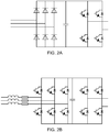
- the transformer 104 has multiple isolated secondary windings to provide an isolated DC supply to each cell. If power regeneration is not required, diode front-end rectifiers can be used in each cell as is shown in the comparative example of Figure 2A .
- the DC-link capacitor voltage is regulated by an active front end (AFE) rectifier which allows real power to flow to the motor during motor operation, and to the grid during regeneration. Additional filters (either L or LCL filters) can be added if an AFE is used since leakage inductance may not be enough to filter the current switching harmonics.
- An H-bridge inverter cell can be realized in either 2-level, 3-level, or higher level topologies.
- the inverter shown in Figure 2B is a 2-level inverter as it can provide voltage at V, 0, or - V .
- a further variant can be a 3-level inverter providing voltage at V , V 2 , 0 , ⁇ V 2 , or - V .
- the principle is to divert the oscillation power from the DC-link to other energy-storing components such as a capacitor or inductor, which allows for much larger fluctuation in voltage or current. This can allow the DC capacitor size to be greatly reduced without adding any large capacitors or inductors.
- Figure 3 shows a typical example of such an active filter 302 (see e.g. R. Wang, F. Wang, D. Boroyevich, and P. Ning, "A high power density single-phase PWM rectifier with active ripple energy storage," IEEE Trans. Power Electron., vol. 26, no. 5, pp. 1378-1383, May 2011 , herein incorporated by reference).
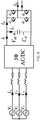
- an AC source is connected to a single phase inverter/rectifier 301, which is then connected to the active filter 302.
- the filter 302 is then connected to a DC source or load 303.
- the oscillation power in C d can be diverted to the capacitor C s .
- the inductor L s and capacitor C s can be of relatively small size.
- the H-bridge converter and active filter shown in Figure 3 may be termed a single-phase pulse width modulation (PWM) converter, and this can be either an inverter or rectifier dependent on the DC side condition (e.g. whether it is a DC source or load).
- PWM pulse width modulation
- the DC side source is from the front-end three-phase rectifier as shown in Figure 1 .
- the single-phase inverters in each leg are connected in series to drive the motor load.
- CHB converters have been widely used at voltage levels including 6.6 kV and above, a disadvantage of CHB converters is the unbalanced characteristic for each inverter cell.
- Each cell of a CHB is a single-phase inverter, where the instantaneous output power is not constant.
- the power has a 2 nd order load current frequency oscillation, which can require a large DC-link capacitance to smooth out the DC-link voltage fluctuations.
- a quantitative analysis for 2 nd order load current frequency oscillation and capacitor size is provided below based on the CHB cell circuit of Figure 4 .
- the voltage fluctuation in the DC-link capacitor is caused by varying current flowing through the capacitor as expressed in equations (1) and (2).
- the three-phase AC/DC rectifier can either be diode front-end or PWM active front end.
- the capacitor current i c is determined by both the front-end rectifier current i i and the rear-end inverter current i o flowing through the DC-link.
- the AC side three-phase currents contain negative sequence 5 th and 11 th order harmonics and positive sequence 7 th and 13 th order harmonics.
- the DC-link rectifier current i i contains 6 th and 12 th order source current frequency oscillation. In a steady state, the DC components of i i and i o are the same to maintain a constant average DC-link voltage V dc .
- the current i i is subjected to the control strategy of the PWM converter as shown in (3).
- i i t d A d B d C ⁇ i u i v i w
- the average value of the single phase inverter DC-link current i o can be calculated using (4) - (7).
- Quantities d 1 and d 3 are duty ratios of the single-phase inverter upper switches, which can be calculated through modulation references, m is the modulation index, ⁇ 0 is the power factor angle of the inverter load, ⁇ a is the phase angle for the single-phase AC modulation reference signal, i a is the output current, and I mo is the output current amplitude.
- the current i o contains both DC and AC quantities, as is shown in (7).
- the AC quantity can cause the DC-link voltage to fluctuate.
- the DC voltage variations are inversely proportional to the frequencies of the AC currents as shown in (8).
- V ⁇ dc 1 2 ⁇ 0 C d ⁇ i oAC
- the DC voltage variation in (8) considers only the single-phase inverter effect. If a diode front-end rectifier was used, there will be 6 th and 12 th order source frequency currents in i i . However, when an active PWM rectifier is used, the current i i is determined by the control strategy and may also contain an AC quantity. The AC current in i i can also cause DC-link voltage fluctuations. The final DC voltage variation will be superposition of the effects caused by both i i and i o .
- the amplitude of the DC-link capacitor AC current i c should attain its minimum value, in order to ensure a relatively stable DC-link voltage V dc with a small sized capacitor C d .
- both the AC and DC components of the rectifier current i i and inverter current i o can be the same or as similar as possible.
- the rectifier current should be controllable, and therefore an AFE rectifier is used.
- the AC side d-axis current can be calculated based on (10), and contains a DC quantity plus a 2 nd order load frequency 2 ⁇ 0 AC quantity.
- the q-axis current can be considered to be zero for unity power factor control.
- a well designed close-loop current controller can track the variable d-axis current reference.
- the CHB cell phase current (corresponding to the transformer secondary winding current) has a cross-coupling effect between two frequencies: 2 ⁇ 0 and ⁇ i , which makes the waveform non-sinusoidal.
- the input source current (corresponding to the transformer primary winding current) is the summation of multiple secondary winding currents from the same phase.
- i uA 1 is the input current of phase u into the A1 cell
- i uB 1 is the input current of phase u into the B1 cell
- i uC 1 is the input current of phase u into the C1 cell.
- the currents i uA 1 , i uB 1 , and i uC1 are input phase currents from cells A1, B2, and C1 respectively:
- the source current is sinusoidal and the cross-coupling effect between the two frequencies 2 ⁇ 0 and ⁇ i is cancelled among the three legs.
- the same conclusion can be drawn from cells An, B n , and C n (where n ⁇ 2).
- the transformer secondary side currents will be controlled to be non-sinusoidal, but the primary side currents can be guaranteed sinusoidal as shown above.
- the input angle ⁇ can be obtained from the primary side and calculated by a phase-locked loop controller, and the value is shared among each of the CHB cells.
- Each cell has its own DC-link voltage close loop control.
- the voltage control output plus the feed-forward control item are set as the d-axis current reference.
- the majority contribution of the current reference is from the feed-forward item, where the contribution from the voltage control output is to cover the system loss and calculation error.
- the q-axis current can be set to be 0 for unity power factor control, or it can be set to a certain value for reactive power compensation.
- the single-phase inverters of the same leg have the same current.
- To calculate the inverter DC average current i o either the measured phase current i a or the current reference i a * can be used.
- the current reference can be obtained from the motor drive control.
- the difference between the desired DC-link voltage V dc * and measured DC-link voltage V dc is determined, and passed to a proportional-integral (PI) controller.
- the output from the PI controller is then added to the load current-feed forward value: i 0 * ⁇ V dc * 1.5 V Sm , producing i sd * , the reference d-axis current.
- the difference between the reference d-axis current i sd * and the measured d-axis current i sd is then determined, and the value passed to another PI controller.
- the output of the PI controller is used to modulate the pulse wave modulation signal which is sent to the AFE of the CHB cell 501. This signal controls the operation of the AFE, such that the rectifier current i i is varied.
- each CHB cell can be designed to have a much smaller volume and weight whilst not requiring any additional hardware components.
- a variant arrangement for the control can be implemented by adding a resonant controller to the inner current loop.
- the d-axis current reference contains a DC quantity plus a 2 nd order load frequency 2 ⁇ 0 AC quantity.
- the PI controller can ensure that the fundamental positive sequence components track the DC command since it can provide infinite gain for the DC component.
- the current loop bandwidth may be set to around 1/10 th of the switching frequency to ensure enough phase margins for stability. For example, if a 4 kHz switching/sampling frequency was used, a 400 Hz current loop bandwidth can be set.
- the 2 nd order load frequency 2 ⁇ 0 AC quantity is subject to the machine rotation speed.
- the maximum frequency of the d-axis current is 120 Hz if one does not consider over speed operation with field weakening control. Even through the frequency is within the current loop bandwidth 400 Hz, the PI controller gain is not enough to achieve zero steady-state error.
- a resonant controller can be added to the current loop as shown in Figure 6 .
- Frequency of the resonant controller 2 ⁇ 0 is related to the machine synchronous speed, which can be tuned in use.
- an LCL filter can be used as shown in Figure 7 . This can reduce the filter size.
- FIG 8 is a schematic of a marine propulsion drive including an electrical system as discussed above.
- a voltage source 801 which is preferably a three-phase AC supply of high voltage is connected to the electrical system 802.
- the electrical system 802 when acting as an AC/AC converter, receives the three-phase AC supply as an input and outputs an AC supply to an electric motor 803.
- the electric motor 803 is connected to a drive 804 e.g. propeller.
- the electrical system 802 controls the output waveform of the AC supply so as to enable the electric motor 803 to perform in the desired manner.
Landscapes
- Engineering & Computer Science (AREA)
- Power Engineering (AREA)
- Inverter Devices (AREA)
Abstract
Description
- The present invention relates to the control of an active front end of an H-bridge converter. Particularly, but not exclusively, the present invention may relate to the application of load current feed-forward control of the active front end of a cascaded H-bridge converter.
- Propulsion of marine vessels by electric drives is an increasing trend in the marine industry. For medium and small vessels, which have installed power of less than around 10 MW, the distribution voltage is expected to remain at 690V AC. For larger vessels however, the operating voltages are much higher, e.g. 3.3 kV or 6.6 kV, as these lead to significant advantages (better efficiency and less cables for example). Generally, these electric drives can be controlled through AC/AC converters such that the output AC waveform is adjustable. Some AC/AC converters are AC/DC-AC converters, so that the input AC waveform is converted to DC (via a DC-link) before being converter to the output AC waveform.
- To achieve operation of these electric drives from a high voltage input, multilevel inverters are preferred. These inverters can be classified into three main categories: neutral point clamped (NPC) inverters; flying capacitor inverters, and cascaded multilevel inverters. For voltage levels higher than 3.3kV, circuits using either NPC or flying capacitor inverters become increasingly complex. The split DC capacitors voltage balance control can also increase in complexity. The non-modularised design is another disadvantage of both the NPC and flying capacitor inverters since these systems have very low redundancy and any single component failure may lead to a whole system failure. The cascaded multilevel inverter do not suffer these deficiencies and has become a popular topology for voltage levels higher than 3.3kV.
- There are many advantages of a cascaded H-bridge (CHB) multilevel converter compared to, for example, a neutral point clamped (NPC) multilevel converter. These include a modularized design with high redundancy, a design which is easy to extend to higher voltages, a low

- In general terms, the invention provides a method of controlling an active front end rectifier in an H-bridge converter such that the current passing through a capacitor in the H-bridge converter is reduced.
- Accordingly, in an aspect, the invention provides an electrical system including:
- a three phase AC input supply;
- three or more H-bridge converter cells, each H-bridge converter cell having:
- an active front end rectifier for receiving the three phase AC input supply and transforming it into a DC supply providing a rectifier current ii ,
- a capacitor suitable to receive a capacitor current ic, the capacitor smoothing the DC supply, and
- an inverter suitable to receive an inverter current io, wherein io = ii - ic, said inverter transforming the received inverter current io into a single phase AC supply; and
- a control subsystem, which provides a signal to each active front end rectifier to vary its respective rectifier current ii such that the difference between the rectifier current ii , provided by the active front end rectifier, and the inverter current io, received by the inverter, is substantially zero.
- Advantageously, this can minimise the value of ic, which allows a capacitor of much smaller capacitance to be used in each H-bridge converter. Depending on the mode of operation, the H-bridge converters may be referred to as H-bridge inverters.
- In another aspect, the invention provides a method of controlling an electrical system including a three phase AC input supply and three or more H-bridge converter cells, each H-bridge converter cell having an active front end rectifier, a capacitor, and an inverter, the method including:
- operating each H-bridge converter cell such that:
- each active front end rectifier receives a three-phase AC input supply and transforms it into a DC supply providing a respective rectifier current ii ;
- each capacitor receives a respective capacitor current ic, the capacitor smoothing the DC supply, and
- each inverter receives a respective inverter current io, wherein io = ii - ic, the inverter transforming the received inverter current io into a single phase AC supply; and
- providing a signal to the active front end rectifier of each H-bridge converter cell, the signal varying the rectifier current ii provided by the active front end rectifier such that the difference between the rectifier current ii , and the inverter current io, is substantially zero.
- In yet another aspect, the invention provides a marine propulsion system including an electric drive, said electric drive being powered by the electrical system according to the first aspect.
- Each aspect of the invention may have any one or, to the extent that they are compatible, any combination of the following optional features.
- The system may include more than three H-bridge converter cells, typically in such examples the number of H-bridge converter cells being a multiple of three.
- The control subsystem may modify said signal based upon a feed-forward load current corresponding to the inverter current io. For example, the control subsystem may include one or more proportional-integral (PI) controllers. The, or each, PI controller may be supplemented by a respective resonant controller.
- The system may further include a pulse width modulator for controlling an ON/OFF duration of switching devices within each active front end rectifier, the ON/OFF durations determining the respective rectifier current ii , wherein the control subsystem provides the signal to each active front end rectifier by instructing the pulse width modulator to modify the ON/OFF durations.
- The pulse width modulator may modify the ON/OFF durations by modifying duty ratios da db dc of the active front end rectifier, wherein the rectifier current ii is described by the equation:

- Each of the H-bridge converter cells may be a single phase H-bridge power cell in a respective cascaded H-bridge converter, each cascaded H-bridge converter may provide a single phase, and the outputs of the three or more cascaded H-bridge converters may connect to provide a three phase AC output supply.
- Each cascaded H-bridge converter may be configured to operate as a multilevel cascade H-bridge converter.
- Each H-bridge converter may further include an LCL filter positioned between its respective active front end rectifier and the three phase AC input supply.
- Embodiments of the invention will now be described by way of example with reference to the accompanying drawings in which:
-
Figure 1 shows a schematic view of a series of cascaded H-bridge converters; -
Figure 2A and 2B show variant arrangements for an H-bridge converter cell; -
Figure 3 shows an example of an active filter; -
Figure 4 shows an example of an H-bridge converter; -
Figure 5 shows a method of controlling a CHB cell; -
Figure 6 shows a variant method of controlling a CHB cell; -
Figure 7 shows a method of controlling a variant CHB cell; and -
Figure 8 shows a schematic of a marine propulsion engine including an electrical system. - As shown in
Figure 1 , a cascaded H-bridge (CHB) multilevel converter is assembled from a number of single phase H-bridge power cells (or modules) e.g. A1 - A4, which are cascaded together to form an equivalent single-phase voltage source. Three single-phase cascades - An isolated DC supply is required for each cell in a CHB multilevel converter. In high power drives, this DC supply can be obtained by a DC-link capacitor supported by a diode rectifier. There are many variations on this basic configuration.
Figure 1 shows an example of a CHB converter with 4 cells in series for each phase: A1 - A4, B1 - B4, and C1 - C4. Thetransformer 104 has multiple isolated secondary windings to provide an isolated DC supply to each cell. If power regeneration is not required, diode front-end rectifiers can be used in each cell as is shown in the comparative example ofFigure 2A . - However, in a variation, which is illustrated in
Figure 2B , the DC-link capacitor voltage is regulated by an active front end (AFE) rectifier which allows real power to flow to the motor during motor operation, and to the grid during regeneration. Additional filters (either L or LCL filters) can be added if an AFE is used since leakage inductance may not be enough to filter the current switching harmonics. An H-bridge inverter cell can be realized in either 2-level, 3-level, or higher level topologies. The inverter shown inFigure 2B is a 2-level inverter as it can provide voltage at V, 0, or - V. However, a further variant can be a 3-level inverter providing voltage at
- For power systems containing a single-phase inverter or rectifier, such as uninterruptible power supplies, grid connected single-phase inverters, or multilevel converters based on CHB cells, there exists a common issue of second-order oscillation of power in the DC-link. Large DC-link capacitance is required to smooth out the DC-link voltage fluctuation.
- It is possible to reduce the DC capacitor size by using an active filter to absorb the second-order oscillation power in the DC-link. The principle is to divert the oscillation power from the DC-link to other energy-storing components such as a capacitor or inductor, which allows for much larger fluctuation in voltage or current. This can allow the DC capacitor size to be greatly reduced without adding any large capacitors or inductors.
-
Figure 3 shows a typical example of such an active filter 302 (see e.g. R. Wang, F. Wang, D. Boroyevich, and P. Ning, "A high power density single-phase PWM rectifier with active ripple energy storage," IEEE Trans. Power Electron., vol. 26, no. 5, pp. 1378-1383, May 2011, herein incorporated by reference). InFigure 3 , an AC source is connected to a single phase inverter/rectifier 301, which is then connected to theactive filter 302. Thefilter 302 is then connected to a DC source orload 303. Through control of theactive filter 302, the oscillation power in Cd can be diverted to the capacitor Cs. The inductor Ls and capacitor Cs can be of relatively small size. When driven by a pulse width modulator (PWM), the H-bridge converter and active filter shown inFigure 3 may be termed a single-phase pulse width modulation (PWM) converter, and this can be either an inverter or rectifier dependent on the DC side condition (e.g. whether it is a DC source or load). For a multilevel CHB inverter, the DC side source is from the front-end three-phase rectifier as shown inFigure 1 . The single-phase inverters in each leg are connected in series to drive the motor load. - Although CHB converters have been widely used at voltage levels including 6.6 kV and above, a disadvantage of CHB converters is the unbalanced characteristic for each inverter cell. Each cell of a CHB is a single-phase inverter, where the instantaneous output power is not constant. The power has a 2nd order load current frequency oscillation, which can require a large DC-link capacitance to smooth out the DC-link voltage fluctuations. A quantitative analysis for 2nd order load current frequency oscillation and capacitor size is provided below based on the CHB cell circuit of
Figure 4 . - The voltage fluctuation in the DC-link capacitor is caused by varying current flowing through the capacitor as expressed in equations (1) and (2). As discussed above, the three-phase AC/DC rectifier can either be diode front-end or PWM active front end. The capacitor current ic is determined by both the front-end rectifier current ii and the rear-end inverter current io flowing through the DC-link.


- For a diode-front end, the AC side three-phase currents contain negative sequence 5th and 11th order harmonics and positive sequence 7th and 13th order harmonics. The DC-link rectifier current ii contains 6th and 12th order source current frequency oscillation. In a steady state, the DC components of ii and io are the same to maintain a constant average DC-link voltage Vdc . For an AFE, the current ii is subjected to the control strategy of the PWM converter as shown in (3).

- The average value of the single phase inverter DC-link current io can be calculated using (4) - (7). Quantities d 1 and d 3 are duty ratios of the single-phase inverter upper switches, which can be calculated through modulation references, m is the modulation index, φ 0 is the power factor angle of the inverter load, θa is the phase angle for the single-phase AC modulation reference signal, ia is the output current, and Imo is the output current amplitude.


- The current io contains both DC and AC quantities, as is shown in (7). The AC quantity can cause the DC-link voltage to fluctuate. Moreover, the DC voltage variations are inversely proportional to the frequencies of the AC currents as shown in (8).

- It should be noted that the DC voltage variation in (8) considers only the single-phase inverter effect. If a diode front-end rectifier was used, there will be 6th and 12th order source frequency currents in ii . However, when an active PWM rectifier is used, the current ii is determined by the control strategy and may also contain an AC quantity. The AC current in ii can also cause DC-link voltage fluctuations. The final DC voltage variation will be superposition of the effects caused by both ii and io.
- Whilst a large size DC-link capacitor can be used to reduce the DC voltage variation, it makes the CHB cell bulky. Further, a multilevel CHB inverter contains many cells. Additional legs and LC filters are required in each cell to construct an active filter suitable to mitigate the second order power in each CHB cell. Moreover, the active filter needs to be controlled properly. This requires hardware modification over the traditional systems and adds control complexity which may be undesirable.
- Preferably, the amplitude of the DC-link capacitor AC current ic should attain its minimum value, in order to ensure a relatively stable DC-link voltage Vdc with a small sized capacitor Cd. To achieve this objective, both the AC and DC components of the rectifier current ii and inverter current io can be the same or as similar as possible. Moreover, the rectifier current should be controllable, and therefore an AFE rectifier is used. The AC and DC side voltage and current relations of an AFE rectifier can be described in (9) based on the power balance theory (when ignoring converter losses) where isd is the d-axis current which represents the three-phase AC input current when considered under a direct-quadrature transformation, and Vsm is the corresponding input phase voltage amplitude :

- Substituting the inverter current io from (7) into the rectifier ii in (9):

- The AC side d-axis current can be calculated based on (10), and contains a DC quantity plus a 2nd order load frequency 2ω 0 AC quantity. The q-axis current can be considered to be zero for unity power factor control. A well designed close-loop current controller can track the variable d-axis current reference.
- The three-phase input currents iu, iv, and iw in a stationary reference frame can be calculated by (11):

- By substituting the d-axis current isd in (10) the phase current can be determined:

- It can been seen that the CHB cell phase current (corresponding to the transformer secondary winding current) has a cross-coupling effect between two frequencies: 2ω 0 and ωi , which makes the waveform non-sinusoidal. The input source current (corresponding to the transformer primary winding current) is the summation of multiple secondary winding currents from the same phase. Considering one cell from each leg, i.e. cells A1, B1, and C1 of
Figure 1 , the primary phase current isAp can be calculated as:
- Where i uA1 is the input current of phase u into the A1 cell, i uB1 is the input current of phase u into the B1 cell, and i uC1 is the input current of phase u into the C1 cell. The above equation assumes that the transformer is not a phase shifted type transformer, which is typical when using a rectifier with an AFE. The currents i uA1 , i uB1, and iuC1 are input phase currents from cells A1, B2, and C1 respectively:


- By substituting (14) and (15) into (13), the transformer primary current can be calculated:

- As is evident from (16), the source current is sinusoidal and the cross-coupling effect between the two frequencies 2 ω 0 and ωi is cancelled among the three legs. The same conclusion can be drawn from cells An, Bn, and Cn (where n ≥ 2). The transformer secondary side currents will be controlled to be non-sinusoidal, but the primary side currents can be guaranteed sinusoidal as shown above.
- Based on this principle, a control strategy is proposed for controlling the AFE rectifier of each
CHB cell 501 as shown inFigure 5 . The input angle θ can be obtained from the primary side and calculated by a phase-locked loop controller, and the value is shared among each of the CHB cells. Each cell has its own DC-link voltage close loop control. The voltage control output plus the feed-forward control item are set as the d-axis current reference. The majority contribution of the current reference is from the feed-forward item, where the contribution from the voltage control output is to cover the system loss and calculation error. The q-axis current can be set to be 0 for unity power factor control, or it can be set to a certain value for reactive power compensation. The single-phase inverters of the same leg have the same current. To calculate the inverter DC average current io, either the measured phase current ia or the current reference
- In the proposed control strategy, the difference between the desired DC-link voltage


CHB cell 501. This signal controls the operation of the AFE, such that the rectifier current ii is varied. - Advantageously, by controlling the AFE rectifier as discussed above, the 2nd order load current ripple will not flow into the capacitor. Therefore as this will not cause capacitor voltage variation, the capacitor size can be greatly reduced. Further, whilst the transformer secondary side currents will be controlled to be non-sinusoidal, the primary side currents can be guaranteed to be sinusoidal. As a result of the decrease in capacitor size, each CHB cell can be designed to have a much smaller volume and weight whilst not requiring any additional hardware components.
- A variant arrangement for the control can be implemented by adding a resonant controller to the inner current loop. It is known that the d-axis current reference contains a DC quantity plus a 2nd order load frequency 2ω 0 AC quantity. The PI controller can ensure that the fundamental positive sequence components track the DC command since it can provide infinite gain for the DC component. The current loop bandwidth may be set to around 1/10th of the switching frequency to ensure enough phase margins for stability. For example, if a 4 kHz switching/sampling frequency was used, a 400 Hz current loop bandwidth can be set. The 2nd order load frequency 2ω 0 AC quantity is subject to the machine rotation speed. For a 60 Hz rated machine, the maximum frequency of the d-axis current is 120 Hz if one does not consider over speed operation with field weakening control. Even through the frequency is within the current loop bandwidth 400 Hz, the PI controller gain is not enough to achieve zero steady-state error.
- To address this problem, a resonant controller can be added to the current loop as shown in
Figure 6 . The frequency of the resonant controller H 2(s) can be set as two times the synchronous frequency of the load machine:
- Frequency of the resonant controller 2ω 0 is related to the machine synchronous speed, which can be tuned in use.
- As a further development, rather than limiting the AFE input filter to a first order inductor filter, an LCL filter can be used as shown in
Figure 7 . This can reduce the filter size. -
Figure 8 is a schematic of a marine propulsion drive including an electrical system as discussed above. Avoltage source 801, which is preferably a three-phase AC supply of high voltage is connected to theelectrical system 802. Theelectrical system 802, when acting as an AC/AC converter, receives the three-phase AC supply as an input and outputs an AC supply to anelectric motor 803. Theelectric motor 803 is connected to adrive 804 e.g. propeller. Theelectrical system 802 controls the output waveform of the AC supply so as to enable theelectric motor 803 to perform in the desired manner. - While the invention has been described in conjunction with the exemplary embodiments described above, many equivalent modifications and variations will be apparent to those skilled in the art when given this disclosure. Accordingly, the exemplary embodiments of the invention set forth above are considered to be illustrative and not limiting. Various changes to the described embodiments may be made without departing from the spirit and scope of the invention.
Claims (13)
- An electrical system including:a three phase AC input supply;three or more H-bridge converter cells, each H-bridge converter cell having:an active front end rectifier for receiving the three phase AC input supply and transforming it into a DC supply providing a rectifier current ii ,a capacitor suitable to receive a capacitor current ic, the capacitor smoothing the DC supply, andan inverter suitable to receive an inverter current io, wherein io = ii - ic, said inverter transforming the received inverter current io into a single phase AC supply; anda control subsystem, which provides a signal to each active front end rectifier to vary its respective rectifier current ii such that the difference between the rectifier current ii , provided by the active front end rectifier, and the inverter current io, received by the inverter, is substantially zero.
- The electrical system of claim 1, wherein the control subsystem modifies said signal based upon a feed-forward load current corresponding to the inverter current io.
- The electrical system of claim 1 or 2 further including a pulse width modulator for controlling an ON/OFF duration of switching devices within each active front end rectifier, the ON/OFF durations determining the respective rectifier current ii , wherein the control subsystem provides the signal to each active front end rectifier by instructing the pulse width modulator to modify the ON/OFF durations.
- The electrical system of claim 3, wherein the pulse width modulator modifies the ON/OFF durations by modifying duty ratios da db dc of the active front end rectifier, wherein the rectifier current ii is described by the equation:

- The electrical system of any preceding claim, wherein each of the H-bridge converter cells is a single phase H-bridge power cell in a respective cascaded H-bridge converter, each cascaded H-bridge converter providing a single phase, and wherein the outputs of said three or more cascaded H-bridge converters connect to provide a three phase AC output supply.
- The electrical system of claim 5, wherein each cascaded H-bridge converter operates as a multilevel cascaded H-bridge converter.
- A marine propulsion system including an electric drive, said electric drive being powered by the electrical system as set out in any preceding claim.
- A method of controlling an electrical system including a three phase AC input supply and three or more H-bridge converter cells, each H-bridge converter cell having an active front end rectifier, a capacitor, and an inverter, the method including:operating each H-bridge converter cell such that:each active front end rectifier receives a three-phase AC input supply and transforms it into a DC supply providing a respective rectifier current ii ;each capacitor receives a respective capacitor current ic, the capacitor smoothing the DC supply, andeach inverter receives a respective inverter current io, wherein io = ii - ic, the inverter transforming the received inverter current io into a single phase AC supply; andproviding a signal to the active front end rectifier of each H-bridge converter cell, the signal varying the rectifier current ii provided by the active front end rectifier such that the difference between the rectifier current ii , and the inverter current io, is substantially zero.
- The method of claim 8, wherein the signal is modified based upon a feed-forward load current corresponding to the inverter current io.
- The method of claim 8 or 9, wherein the electrical system further includes a pulse width modulator which controls an ON/OFF duration of switching devices within each active front end rectifier, the ON/OFF durations determining the respective rectifier current ii , the signal instructing the pulse width modulator to modify the ON/OFF durations.
- The method of claim 10, wherein the ON/OFF durations is modified by modifying duty ratios da db dc of the active front end rectifier, wherein the rectifier current ii is described by the equation:

- The method of any of claims 8 - 11, wherein each of the H-bridge converter cells is a single phase H-bridge power cell in a respective cascaded H-bridge converter, each cascaded H-bridge converter providing a single phase, and wherein the outputs of said three or more cascaded H-bridge converters connect to provide a three phase AC output supply.
- The method of claim 12, wherein each cascaded H-bridge converter operates as a multilevel cascaded H-bridge converter.
Applications Claiming Priority (1)
| Application Number | Priority Date | Filing Date | Title |
|---|---|---|---|
| GBGB1610369.9A GB201610369D0 (en) | 2016-06-15 | 2016-06-15 | Control of an electrical converter |
Publications (2)
| Publication Number | Publication Date |
|---|---|
| EP3258588A1 true EP3258588A1 (en) | 2017-12-20 |
| EP3258588B1 EP3258588B1 (en) | 2019-05-08 |
Family
ID=56894665
Family Applications (1)
| Application Number | Title | Priority Date | Filing Date |
|---|---|---|---|
| EP17172121.0A Active EP3258588B1 (en) | 2016-06-15 | 2017-05-22 | Control of an electrical converter |
Country Status (3)
| Country | Link |
|---|---|
| US (1) | US10038367B2 (en) |
| EP (1) | EP3258588B1 (en) |
| GB (1) | GB201610369D0 (en) |
Cited By (2)
| Publication number | Priority date | Publication date | Assignee | Title |
|---|---|---|---|---|
| WO2019121251A1 (en) * | 2017-12-21 | 2019-06-27 | Sma Solar Technology Ag | Converter comprising at least one converter module with three bridge branches, operating method, and use of such a converter |
| WO2020125072A1 (en) * | 2018-12-19 | 2020-06-25 | 厦门市必易微电子技术有限公司 | Stepless speed regulation circuit and method for single-phase motor |
Families Citing this family (21)
| Publication number | Priority date | Publication date | Assignee | Title |
|---|---|---|---|---|
| US10128775B2 (en) * | 2014-11-04 | 2018-11-13 | Mitsubishi Electric Corporation | Motor drive apparatus and air conditioner |
| JP6430028B2 (en) * | 2015-10-01 | 2018-11-28 | 三菱電機株式会社 | Power converter and air conditioner using the same |
| US10130016B2 (en) * | 2016-08-26 | 2018-11-13 | TECO—Westinghouse Motor Company | Modular size multi-megawatt silicon carbide-based medium voltage conversion system |
| KR20180064670A (en) * | 2016-12-06 | 2018-06-15 | 엘에스산전 주식회사 | Converter of an inactive power compensator and method of controlling the same |
| US10153710B1 (en) * | 2017-07-25 | 2018-12-11 | Delta Electronics, Inc. | Power supply and control method thereof |
| US10270327B1 (en) * | 2017-10-13 | 2019-04-23 | Deere & Company | Voltage sensor-less position detection in an active front end |
| US10295581B2 (en) * | 2017-10-13 | 2019-05-21 | Deere & Company | Voltage sensor-less position detection in an active front end |
| WO2019200592A1 (en) * | 2018-04-19 | 2019-10-24 | Abb Schweiz Ag | System and method for power conversion |
| CN108988707A (en) * | 2018-05-28 | 2018-12-11 | 珠海格力电器股份有限公司 | Current loop bandwidth expanding method and device, storage medium and servo driver |
| CN109361206B (en) * | 2018-09-28 | 2022-05-10 | 哈尔滨中创电气技术有限公司 | An energy control method for ship medium voltage grid structure based on multi-terminal DC-DC converter |
| EP3709497B1 (en) * | 2019-03-14 | 2022-12-28 | ABB Schweiz AG | Cascaded pulse width modulation converter control |
| DE102019109629A1 (en) | 2019-04-11 | 2020-10-15 | Rittal Gmbh & Co. Kg | Busbar system with at least one busbar held in a touch protection housing |
| DE102019118927A1 (en) * | 2019-07-12 | 2021-01-14 | Vacon Oy | DC link charging arrangement and method for charging a DC link capacitor |
| US11469685B2 (en) | 2019-08-21 | 2022-10-11 | Rockwell Automation Technologies, Inc. | Filter and AFE power cell phase control |
| US20210058003A1 (en) * | 2019-08-21 | 2021-02-25 | Rockwell Automation Technologies, Inc. | Filter and afe power cell phase control |
| CN110557074B (en) * | 2019-08-27 | 2020-12-29 | 天津大学 | Predictive Current Control Method for Cascaded H-Bridge Inverter Permanent Magnet Motor Systems |
| US11211879B2 (en) | 2019-09-23 | 2021-12-28 | Rockwell Automation Technologies, Inc. | Capacitor size reduction and lifetime extension for cascaded H-bridge drives |
| US11569759B2 (en) * | 2020-01-03 | 2023-01-31 | Westinghouse Air Brake Technologies Corporation | System with active filter for a battery |
| CN112332445B (en) * | 2020-09-29 | 2022-11-18 | 广西大学 | LCL grid-connected inverter indirect current control method based on instruction current compensation |
| US11437938B2 (en) * | 2020-09-29 | 2022-09-06 | Rockwell Automation Technologies, Inc. | Systems and methods of multi-motor regenerative drive |
| US11342878B1 (en) | 2021-04-09 | 2022-05-24 | Rockwell Automation Technologies, Inc. | Regenerative medium voltage drive (Cascaded H Bridge) with reduced number of sensors |
Citations (3)
| Publication number | Priority date | Publication date | Assignee | Title |
|---|---|---|---|---|
| DE10042938A1 (en) * | 1999-09-01 | 2001-03-15 | Robicon Corp | Motor drive has power transformer secondary circuits coupled to individual power cells regulated for reduction of harmonics |
| US20030223251A1 (en) * | 2002-06-04 | 2003-12-04 | Hammond Peter W. | Control method and apparatus to reduce current through DC capacitor linking two static converters |
| US20100142234A1 (en) * | 2008-12-31 | 2010-06-10 | Mehdi Abolhassani | Partial regeneration in a multi-level power inverter |
Family Cites Families (38)
| Publication number | Priority date | Publication date | Assignee | Title |
|---|---|---|---|---|
| US4879639A (en) * | 1987-05-11 | 1989-11-07 | Fuji Electric Co., Ltd. | Power converter for driving an AC motor at a variable speed |
| US6014323A (en) * | 1997-08-08 | 2000-01-11 | Robicon Corporation | Multiphase power converter |
| US6031738A (en) | 1998-06-16 | 2000-02-29 | Wisconsin Alumni Research Foundation | DC bus voltage balancing and control in multilevel inverters |
| US6697271B2 (en) | 2000-08-16 | 2004-02-24 | Northrop Grumman Corporation | Cascaded multi-level H-bridge drive |
| JP4601044B2 (en) * | 2004-08-30 | 2010-12-22 | 日立アプライアンス株式会社 | Power converter and air conditioner equipped with the power converter |
| JP4645139B2 (en) * | 2004-10-04 | 2011-03-09 | ダイキン工業株式会社 | Power converter |
| FI121491B (en) * | 2004-11-11 | 2010-11-30 | Vacon Oyj | Frequency converter overvoltage protection |
| US7508147B2 (en) * | 2005-05-19 | 2009-03-24 | Siemens Energy & Automation, Inc. | Variable-frequency drive with regeneration capability |
| RU2007149319A (en) * | 2005-05-27 | 2009-07-10 | Сименс Энерджи Энд Отомейшн, Инк. (Us) | FUNCTIONING OF INVERTERS WITH REMOTE MODULATION |
| US7368890B2 (en) * | 2006-02-07 | 2008-05-06 | Rockwell Automation Technologies, Inc. | Power converter with active discharging for improved auto-restart capability |
| US7274576B1 (en) * | 2006-03-01 | 2007-09-25 | Rockwell Automation Technologies, Inc. | Power converter with reduced common mode voltage |
| US8397085B2 (en) * | 2007-09-24 | 2013-03-12 | Siemens Industry, Inc. | Master controller containing a control processor configured to receive power cell control information and a host processor configured to receive command and status information |
| US7710082B2 (en) * | 2007-10-18 | 2010-05-04 | Instituto Potosino De Investigacion Cientifica Y Technologica (Ipicyt) | Controller for the three-phase cascade multilevel converter used as shunt active filter in unbalanced operation with guaranteed capacitors voltages balance |
| US8125177B2 (en) * | 2008-06-13 | 2012-02-28 | Baker Hughes Incorporated | System and method for adding voltages of power modules in variable frequency drives |
| ES2571939T3 (en) * | 2008-11-21 | 2016-05-27 | Otis Elevator Co | Operation of a three-phase regenerative drive from mixed DC and AC single phase AC power supplies |
| US8188693B2 (en) * | 2009-11-04 | 2012-05-29 | Rockwell Automation Technologies, Inc. | DC bus boost method and system for regenerative brake |
| US8223511B2 (en) * | 2010-06-07 | 2012-07-17 | Rockwell Automation Technologies, Inc. | Common mode voltage reduction apparatus and method for current source converter based drive |
| US8503207B2 (en) * | 2010-09-29 | 2013-08-06 | Rockwell Automation Technologies, Inc. | Discontinuous pulse width drive modulation method and apparatus for reduction of common-mode voltage in power conversion systems |
| FI124139B (en) * | 2011-01-19 | 2014-03-31 | Vacon Oyj | Device for transmitting electrical power |
| US8570775B2 (en) * | 2011-02-17 | 2013-10-29 | Rockwell Automation Technologies, Inc. | CMV reduction under bus transient condition |
| CN103066859A (en) * | 2011-10-19 | 2013-04-24 | 台达电子企业管理(上海)有限公司 | High-power high-voltage frequency inverter power unit |
| CN103107689A (en) * | 2011-11-11 | 2013-05-15 | 台达电子企业管理(上海)有限公司 | A cascaded frequency converter, power unit and bypass module thereof |
| US8988026B2 (en) * | 2012-07-31 | 2015-03-24 | Rockwell Automation Technologies, Inc. | Single phase operation of a three-phase drive system |
| US9007787B2 (en) * | 2012-08-13 | 2015-04-14 | Rockwell Automation Technologies, Inc. | Method and apparatus for bypassing Cascaded H-Bridge (CHB) power cells and power sub cell for multilevel inverter |
| US9876347B2 (en) * | 2012-08-30 | 2018-01-23 | Siemens Aktiengesellschaft | Apparatus and methods for restoring power cell functionality in multi-cell power supplies |
| KR101792039B1 (en) * | 2013-08-08 | 2017-11-01 | 엘에스산전 주식회사 | Method for determining phase angle in phase shift transformer for mrdium-voltage inverter |
| US9318992B2 (en) * | 2013-08-22 | 2016-04-19 | Yaskawa America, Inc. | Drive circuit for a pre-phase AC motor |
| US9374021B2 (en) * | 2013-12-16 | 2016-06-21 | Rockwell Automation Technologies, Inc. | PWM output voltage measurement apparatus and method |
| US9787212B2 (en) * | 2014-05-05 | 2017-10-10 | Rockwell Automation Technologies, Inc. | Motor drive with silicon carbide MOSFET switches |
| JP5820021B1 (en) * | 2014-06-13 | 2015-11-24 | ファナック株式会社 | Motor control device having charging resistance protection means |
| CN104079182B (en) * | 2014-06-18 | 2017-11-21 | 华为技术有限公司 | Inverter system |
| JP6446855B2 (en) * | 2014-06-20 | 2019-01-09 | 株式会社安川電機 | Power conversion device, state detection device, and state detection method |
| JP5946880B2 (en) * | 2014-09-26 | 2016-07-06 | ファナック株式会社 | Motor control device having LCL filter protection function |
| CN204597784U (en) * | 2015-03-24 | 2015-08-26 | 光宝科技股份有限公司 | Detection circuit and three-phase AC/AC power conversion device with detection circuit |
| KR20160122921A (en) * | 2015-04-14 | 2016-10-25 | 엘에스산전 주식회사 | Gate driver for driving inverter |
| US10177702B2 (en) * | 2015-08-12 | 2019-01-08 | Samsung Electronics Co., Ltd. | Conduction noise filtering circuit, inverting device, and compressor |
| KR102485705B1 (en) * | 2016-02-18 | 2023-01-05 | 엘에스일렉트릭(주) | Method for controlling three phase equivalent voltage of multilevel inverter |
| US9847733B2 (en) * | 2016-05-12 | 2017-12-19 | Rockwell Automation Technologies, Inc. | Power conversion system with DC bus regulation for abnormal grid condition ride through |
-
2016
- 2016-06-15 GB GBGB1610369.9A patent/GB201610369D0/en not_active Ceased
-
2017
- 2017-05-22 US US15/601,050 patent/US10038367B2/en active Active
- 2017-05-22 EP EP17172121.0A patent/EP3258588B1/en active Active
Patent Citations (3)
| Publication number | Priority date | Publication date | Assignee | Title |
|---|---|---|---|---|
| DE10042938A1 (en) * | 1999-09-01 | 2001-03-15 | Robicon Corp | Motor drive has power transformer secondary circuits coupled to individual power cells regulated for reduction of harmonics |
| US20030223251A1 (en) * | 2002-06-04 | 2003-12-04 | Hammond Peter W. | Control method and apparatus to reduce current through DC capacitor linking two static converters |
| US20100142234A1 (en) * | 2008-12-31 | 2010-06-10 | Mehdi Abolhassani | Partial regeneration in a multi-level power inverter |
Non-Patent Citations (1)
| Title |
|---|
| R. WANG; F. WANG; D. BOROYEVICH; P. NING: "A high power density single-phase PWM rectifier with active ripple energy storage", IEEE TRANS. POWER ELECTRON., vol. 26, no. 5, May 2011 (2011-05-01), pages 1378 - 1383 |
Cited By (3)
| Publication number | Priority date | Publication date | Assignee | Title |
|---|---|---|---|---|
| WO2019121251A1 (en) * | 2017-12-21 | 2019-06-27 | Sma Solar Technology Ag | Converter comprising at least one converter module with three bridge branches, operating method, and use of such a converter |
| WO2020125072A1 (en) * | 2018-12-19 | 2020-06-25 | 厦门市必易微电子技术有限公司 | Stepless speed regulation circuit and method for single-phase motor |
| US10972038B2 (en) | 2018-12-19 | 2021-04-06 | Xiamen Kiwi Instruments Corporation | Stepless motor driving circuit and associated driving method |
Also Published As
| Publication number | Publication date |
|---|---|
| GB201610369D0 (en) | 2016-07-27 |
| US10038367B2 (en) | 2018-07-31 |
| US20170366082A1 (en) | 2017-12-21 |
| EP3258588B1 (en) | 2019-05-08 |
Similar Documents
| Publication | Publication Date | Title |
|---|---|---|
| EP3258588B1 (en) | Control of an electrical converter | |
| Jung et al. | Control strategy for improved dynamic performance of variable-speed drives with modular multilevel converter | |
| EP2827490B1 (en) | System and method for unified common mode voltage injection | |
| US9793827B2 (en) | Power conversion system and method | |
| Jung et al. | Control of the modular multilevel converter for variable-speed drives | |
| Diab et al. | A modular multilevel converter with isolated energy-balancing modules for MV drives incorporating symmetrical six-phase machines | |
| Kumara et al. | Performance improvements of power converters for high power induction motor drive | |
| Wang et al. | An AC side-active power decoupling modular for single phase power converter | |
| CN113991725B (en) | An offshore wind power flexible direct current transmission system and control method thereof | |
| RU157682U1 (en) | HIGH POWER HIGH POWER FREQUENCY CONVERTER WITH ACTIVE RECTIFIERS | |
| de Sousa et al. | Modeling and control of a modular multilevel converter for medium voltage drives rectifier applications | |
| Sau et al. | Reduction of capacitor ripple voltage and current in Modular Multilevel Converter based variable speed drives | |
| Wang et al. | Step-up switched-capacitor multilevel inverter employing multiple inputs with reduced switches | |
| Rajesh et al. | A shunt active power filter for 12 pulse converter using source current detection approach | |
| Aameria et al. | Design of a novel dual-output multilevel pwm converter | |
| EP3386085A1 (en) | Electrical system | |
| Brando et al. | Voltage fluctuation smoothing in the half-bridge cells of MMC for induction motor drives using recirculation currents SVM control | |
| Rodríguez et al. | High power synchronous machine fed by a cascaded regenerative inverter | |
| Si et al. | Control strategy and simulation of a modular multilevel converter (MMC) based pump-back system for variable speed drive application | |
| Almeida et al. | Single-phase to three-phase ac-dc-ac converter based on cascaded transformers rectifier and open-end winding induction motor | |
| Ebrahimi et al. | An Active Capacitor Voltage Balancing Method for a Four-Level Single Flying Capacitor Converter | |
| Medina | Design and control of single-phase modular multilevel converter | |
| Hassanabad et al. | Design and simulation of space vector pulse width modulation inverter based transformer-less in small wind turbines | |
| Perera | Power Conversion Techniques Using Dual Inverter Structures | |
| Mochidate et al. | Total volume reduction of passive components in Grid-connected converters by introducing flying capacitor multilevel topology |
Legal Events
| Date | Code | Title | Description |
|---|---|---|---|
| PUAI | Public reference made under article 153(3) epc to a published international application that has entered the european phase |
Free format text: ORIGINAL CODE: 0009012 |
|
| STAA | Information on the status of an ep patent application or granted ep patent |
Free format text: STATUS: THE APPLICATION HAS BEEN PUBLISHED |
|
| AK | Designated contracting states |
Kind code of ref document: A1 Designated state(s): AL AT BE BG CH CY CZ DE DK EE ES FI FR GB GR HR HU IE IS IT LI LT LU LV MC MK MT NL NO PL PT RO RS SE SI SK SM TR |
|
| AX | Request for extension of the european patent |
Extension state: BA ME |
|
| STAA | Information on the status of an ep patent application or granted ep patent |
Free format text: STATUS: REQUEST FOR EXAMINATION WAS MADE |
|
| 17P | Request for examination filed |
Effective date: 20180611 |
|
| RBV | Designated contracting states (corrected) |
Designated state(s): AL AT BE BG CH CY CZ DE DK EE ES FI FR GB GR HR HU IE IS IT LI LT LU LV MC MK MT NL NO PL PT RO RS SE SI SK SM TR |
|
| GRAP | Despatch of communication of intention to grant a patent |
Free format text: ORIGINAL CODE: EPIDOSNIGR1 |
|
| STAA | Information on the status of an ep patent application or granted ep patent |
Free format text: STATUS: GRANT OF PATENT IS INTENDED |
|
| GRAS | Grant fee paid |
Free format text: ORIGINAL CODE: EPIDOSNIGR3 |
|
| GRAA | (expected) grant |
Free format text: ORIGINAL CODE: 0009210 |
|
| STAA | Information on the status of an ep patent application or granted ep patent |
Free format text: STATUS: THE PATENT HAS BEEN GRANTED |
|
| INTG | Intention to grant announced |
Effective date: 20190320 |
|
| AK | Designated contracting states |
Kind code of ref document: B1 Designated state(s): AL AT BE BG CH CY CZ DE DK EE ES FI FR GB GR HR HU IE IS IT LI LT LU LV MC MK MT NL NO PL PT RO RS SE SI SK SM TR |
|
| REG | Reference to a national code |
Ref country code: GB Ref legal event code: FG4D |
|
| REG | Reference to a national code |
Ref country code: CH Ref legal event code: EP Ref country code: AT Ref legal event code: REF Ref document number: 1131763 Country of ref document: AT Kind code of ref document: T Effective date: 20190515 |
|
| REG | Reference to a national code |
Ref country code: DE Ref legal event code: R096 Ref document number: 602017003779 Country of ref document: DE Ref country code: IE Ref legal event code: FG4D |
|
| REG | Reference to a national code |
Ref country code: NL Ref legal event code: MP Effective date: 20190508 |
|
| REG | Reference to a national code |
Ref country code: LT Ref legal event code: MG4D |
|
| PG25 | Lapsed in a contracting state [announced via postgrant information from national office to epo] |
Ref country code: SE Free format text: LAPSE BECAUSE OF FAILURE TO SUBMIT A TRANSLATION OF THE DESCRIPTION OR TO PAY THE FEE WITHIN THE PRESCRIBED TIME-LIMIT Effective date: 20190508 Ref country code: PT Free format text: LAPSE BECAUSE OF FAILURE TO SUBMIT A TRANSLATION OF THE DESCRIPTION OR TO PAY THE FEE WITHIN THE PRESCRIBED TIME-LIMIT Effective date: 20190908 Ref country code: AL Free format text: LAPSE BECAUSE OF FAILURE TO SUBMIT A TRANSLATION OF THE DESCRIPTION OR TO PAY THE FEE WITHIN THE PRESCRIBED TIME-LIMIT Effective date: 20190508 Ref country code: ES Free format text: LAPSE BECAUSE OF FAILURE TO SUBMIT A TRANSLATION OF THE DESCRIPTION OR TO PAY THE FEE WITHIN THE PRESCRIBED TIME-LIMIT Effective date: 20190508 Ref country code: NL Free format text: LAPSE BECAUSE OF FAILURE TO SUBMIT A TRANSLATION OF THE DESCRIPTION OR TO PAY THE FEE WITHIN THE PRESCRIBED TIME-LIMIT Effective date: 20190508 Ref country code: LT Free format text: LAPSE BECAUSE OF FAILURE TO SUBMIT A TRANSLATION OF THE DESCRIPTION OR TO PAY THE FEE WITHIN THE PRESCRIBED TIME-LIMIT Effective date: 20190508 Ref country code: HR Free format text: LAPSE BECAUSE OF FAILURE TO SUBMIT A TRANSLATION OF THE DESCRIPTION OR TO PAY THE FEE WITHIN THE PRESCRIBED TIME-LIMIT Effective date: 20190508 Ref country code: NO Free format text: LAPSE BECAUSE OF FAILURE TO SUBMIT A TRANSLATION OF THE DESCRIPTION OR TO PAY THE FEE WITHIN THE PRESCRIBED TIME-LIMIT Effective date: 20190808 Ref country code: FI Free format text: LAPSE BECAUSE OF FAILURE TO SUBMIT A TRANSLATION OF THE DESCRIPTION OR TO PAY THE FEE WITHIN THE PRESCRIBED TIME-LIMIT Effective date: 20190508 |
|
| PG25 | Lapsed in a contracting state [announced via postgrant information from national office to epo] |
Ref country code: GR Free format text: LAPSE BECAUSE OF FAILURE TO SUBMIT A TRANSLATION OF THE DESCRIPTION OR TO PAY THE FEE WITHIN THE PRESCRIBED TIME-LIMIT Effective date: 20190809 Ref country code: LV Free format text: LAPSE BECAUSE OF FAILURE TO SUBMIT A TRANSLATION OF THE DESCRIPTION OR TO PAY THE FEE WITHIN THE PRESCRIBED TIME-LIMIT Effective date: 20190508 Ref country code: BG Free format text: LAPSE BECAUSE OF FAILURE TO SUBMIT A TRANSLATION OF THE DESCRIPTION OR TO PAY THE FEE WITHIN THE PRESCRIBED TIME-LIMIT Effective date: 20190808 Ref country code: RS Free format text: LAPSE BECAUSE OF FAILURE TO SUBMIT A TRANSLATION OF THE DESCRIPTION OR TO PAY THE FEE WITHIN THE PRESCRIBED TIME-LIMIT Effective date: 20190508 |
|
| REG | Reference to a national code |
Ref country code: AT Ref legal event code: MK05 Ref document number: 1131763 Country of ref document: AT Kind code of ref document: T Effective date: 20190508 |
|
| PG25 | Lapsed in a contracting state [announced via postgrant information from national office to epo] |
Ref country code: AT Free format text: LAPSE BECAUSE OF FAILURE TO SUBMIT A TRANSLATION OF THE DESCRIPTION OR TO PAY THE FEE WITHIN THE PRESCRIBED TIME-LIMIT Effective date: 20190508 Ref country code: DK Free format text: LAPSE BECAUSE OF FAILURE TO SUBMIT A TRANSLATION OF THE DESCRIPTION OR TO PAY THE FEE WITHIN THE PRESCRIBED TIME-LIMIT Effective date: 20190508 Ref country code: EE Free format text: LAPSE BECAUSE OF FAILURE TO SUBMIT A TRANSLATION OF THE DESCRIPTION OR TO PAY THE FEE WITHIN THE PRESCRIBED TIME-LIMIT Effective date: 20190508 Ref country code: SK Free format text: LAPSE BECAUSE OF FAILURE TO SUBMIT A TRANSLATION OF THE DESCRIPTION OR TO PAY THE FEE WITHIN THE PRESCRIBED TIME-LIMIT Effective date: 20190508 Ref country code: CZ Free format text: LAPSE BECAUSE OF FAILURE TO SUBMIT A TRANSLATION OF THE DESCRIPTION OR TO PAY THE FEE WITHIN THE PRESCRIBED TIME-LIMIT Effective date: 20190508 Ref country code: RO Free format text: LAPSE BECAUSE OF FAILURE TO SUBMIT A TRANSLATION OF THE DESCRIPTION OR TO PAY THE FEE WITHIN THE PRESCRIBED TIME-LIMIT Effective date: 20190508 |
|
| REG | Reference to a national code |
Ref country code: BE Ref legal event code: MM Effective date: 20190531 |
|
| REG | Reference to a national code |
Ref country code: DE Ref legal event code: R097 Ref document number: 602017003779 Country of ref document: DE |
|
| RAP2 | Party data changed (patent owner data changed or rights of a patent transferred) |
Owner name: ROLLS-ROYCE PLC |
|
| PG25 | Lapsed in a contracting state [announced via postgrant information from national office to epo] |
Ref country code: MC Free format text: LAPSE BECAUSE OF FAILURE TO SUBMIT A TRANSLATION OF THE DESCRIPTION OR TO PAY THE FEE WITHIN THE PRESCRIBED TIME-LIMIT Effective date: 20190508 Ref country code: IT Free format text: LAPSE BECAUSE OF FAILURE TO SUBMIT A TRANSLATION OF THE DESCRIPTION OR TO PAY THE FEE WITHIN THE PRESCRIBED TIME-LIMIT Effective date: 20190508 Ref country code: SM Free format text: LAPSE BECAUSE OF FAILURE TO SUBMIT A TRANSLATION OF THE DESCRIPTION OR TO PAY THE FEE WITHIN THE PRESCRIBED TIME-LIMIT Effective date: 20190508 Ref country code: LU Free format text: LAPSE BECAUSE OF NON-PAYMENT OF DUE FEES Effective date: 20190522 |
|
| PLBE | No opposition filed within time limit |
Free format text: ORIGINAL CODE: 0009261 |
|
| STAA | Information on the status of an ep patent application or granted ep patent |
Free format text: STATUS: NO OPPOSITION FILED WITHIN TIME LIMIT |
|
| PG25 | Lapsed in a contracting state [announced via postgrant information from national office to epo] |
Ref country code: TR Free format text: LAPSE BECAUSE OF FAILURE TO SUBMIT A TRANSLATION OF THE DESCRIPTION OR TO PAY THE FEE WITHIN THE PRESCRIBED TIME-LIMIT Effective date: 20190508 |
|
| 26N | No opposition filed |
Effective date: 20200211 |
|
| PG25 | Lapsed in a contracting state [announced via postgrant information from national office to epo] |
Ref country code: PL Free format text: LAPSE BECAUSE OF FAILURE TO SUBMIT A TRANSLATION OF THE DESCRIPTION OR TO PAY THE FEE WITHIN THE PRESCRIBED TIME-LIMIT Effective date: 20190508 Ref country code: IE Free format text: LAPSE BECAUSE OF NON-PAYMENT OF DUE FEES Effective date: 20190522 |
|
| PG25 | Lapsed in a contracting state [announced via postgrant information from national office to epo] |
Ref country code: BE Free format text: LAPSE BECAUSE OF NON-PAYMENT OF DUE FEES Effective date: 20190531 Ref country code: SI Free format text: LAPSE BECAUSE OF FAILURE TO SUBMIT A TRANSLATION OF THE DESCRIPTION OR TO PAY THE FEE WITHIN THE PRESCRIBED TIME-LIMIT Effective date: 20190508 |
|
| PG25 | Lapsed in a contracting state [announced via postgrant information from national office to epo] |
Ref country code: LI Free format text: LAPSE BECAUSE OF NON-PAYMENT OF DUE FEES Effective date: 20200531 Ref country code: CH Free format text: LAPSE BECAUSE OF NON-PAYMENT OF DUE FEES Effective date: 20200531 |
|
| PG25 | Lapsed in a contracting state [announced via postgrant information from national office to epo] |
Ref country code: CY Free format text: LAPSE BECAUSE OF FAILURE TO SUBMIT A TRANSLATION OF THE DESCRIPTION OR TO PAY THE FEE WITHIN THE PRESCRIBED TIME-LIMIT Effective date: 20190508 |
|
| PG25 | Lapsed in a contracting state [announced via postgrant information from national office to epo] |
Ref country code: IS Free format text: LAPSE BECAUSE OF FAILURE TO SUBMIT A TRANSLATION OF THE DESCRIPTION OR TO PAY THE FEE WITHIN THE PRESCRIBED TIME-LIMIT Effective date: 20190908 |
|
| PG25 | Lapsed in a contracting state [announced via postgrant information from national office to epo] |
Ref country code: MT Free format text: LAPSE BECAUSE OF FAILURE TO SUBMIT A TRANSLATION OF THE DESCRIPTION OR TO PAY THE FEE WITHIN THE PRESCRIBED TIME-LIMIT Effective date: 20190508 Ref country code: HU Free format text: LAPSE BECAUSE OF FAILURE TO SUBMIT A TRANSLATION OF THE DESCRIPTION OR TO PAY THE FEE WITHIN THE PRESCRIBED TIME-LIMIT; INVALID AB INITIO Effective date: 20170522 |
|
| PG25 | Lapsed in a contracting state [announced via postgrant information from national office to epo] |
Ref country code: MK Free format text: LAPSE BECAUSE OF FAILURE TO SUBMIT A TRANSLATION OF THE DESCRIPTION OR TO PAY THE FEE WITHIN THE PRESCRIBED TIME-LIMIT Effective date: 20190508 |
|
| P01 | Opt-out of the competence of the unified patent court (upc) registered |
Effective date: 20230528 |
|
| PGFP | Annual fee paid to national office [announced via postgrant information from national office to epo] |
Ref country code: DE Payment date: 20250528 Year of fee payment: 9 |
|
| PGFP | Annual fee paid to national office [announced via postgrant information from national office to epo] |
Ref country code: FR Payment date: 20250526 Year of fee payment: 9 |
|
| PGFP | Annual fee paid to national office [announced via postgrant information from national office to epo] |
Ref country code: GB Payment date: 20260313 Year of fee payment: 10 |