EP3258509A1 - 9,9-disubstituted 9,10-dihydroacridine compounds and their use for doping crystalline organic semiconductors - Google Patents
9,9-disubstituted 9,10-dihydroacridine compounds and their use for doping crystalline organic semiconductors Download PDFInfo
- Publication number
- EP3258509A1 EP3258509A1 EP16174445.3A EP16174445A EP3258509A1 EP 3258509 A1 EP3258509 A1 EP 3258509A1 EP 16174445 A EP16174445 A EP 16174445A EP 3258509 A1 EP3258509 A1 EP 3258509A1
- Authority
- EP
- European Patent Office
- Prior art keywords
- optionally substituted
- dihydroacridine
- moiety
- organic
- composition
- Prior art date
- Legal status (The legal status is an assumption and is not a legal conclusion. Google has not performed a legal analysis and makes no representation as to the accuracy of the status listed.)
- Withdrawn
Links
- 239000004065 semiconductor Substances 0.000 title claims abstract description 42
- -1 9,9-disubstituted 9,10-dihydroacridine compounds Chemical class 0.000 title claims description 19
- 239000000203 mixture Substances 0.000 claims abstract description 63
- 150000001875 compounds Chemical class 0.000 claims abstract description 58
- 125000001072 heteroaryl group Chemical group 0.000 claims abstract description 13
- 125000001183 hydrocarbyl group Chemical group 0.000 claims abstract description 10
- 238000000034 method Methods 0.000 claims description 20
- 239000000758 substrate Substances 0.000 claims description 16
- 239000002904 solvent Substances 0.000 claims description 13
- 125000004122 cyclic group Chemical group 0.000 claims description 12
- 230000005669 field effect Effects 0.000 claims description 11
- 239000003960 organic solvent Substances 0.000 claims description 11
- 238000004519 manufacturing process Methods 0.000 claims description 10
- 238000001704 evaporation Methods 0.000 claims description 3
- ICPSWZFVWAPUKF-UHFFFAOYSA-N 1,1'-spirobi[fluorene] Chemical group C1=CC=C2C=C3C4(C=5C(C6=CC=CC=C6C=5)=CC=C4)C=CC=C3C2=C1 ICPSWZFVWAPUKF-UHFFFAOYSA-N 0.000 claims description 2
- 125000003107 substituted aryl group Chemical group 0.000 claims description 2
- 125000003118 aryl group Chemical group 0.000 abstract description 13
- 125000001424 substituent group Chemical group 0.000 description 26
- CXWXQJXEFPUFDZ-UHFFFAOYSA-N tetralin Chemical compound C1=CC=C2CCCCC2=C1 CXWXQJXEFPUFDZ-UHFFFAOYSA-N 0.000 description 22
- 125000004432 carbon atom Chemical group C* 0.000 description 20
- IYYZUPMFVPLQIF-UHFFFAOYSA-N dibenzothiophene Chemical compound C1=CC=C2C3=CC=CC=C3SC2=C1 IYYZUPMFVPLQIF-UHFFFAOYSA-N 0.000 description 18
- UJOBWOGCFQCDNV-UHFFFAOYSA-N 9H-carbazole Chemical compound C1=CC=C2C3=CC=CC=C3NC2=C1 UJOBWOGCFQCDNV-UHFFFAOYSA-N 0.000 description 16
- 239000011230 binding agent Substances 0.000 description 14
- 125000000217 alkyl group Chemical group 0.000 description 10
- 150000003384 small molecules Chemical group 0.000 description 10
- UHOVQNZJYSORNB-UHFFFAOYSA-N Benzene Chemical compound C1=CC=CC=C1 UHOVQNZJYSORNB-UHFFFAOYSA-N 0.000 description 9
- 238000009472 formulation Methods 0.000 description 9
- 239000011521 glass Substances 0.000 description 7
- KFZMGEQAYNKOFK-UHFFFAOYSA-N Isopropanol Chemical compound CC(C)O KFZMGEQAYNKOFK-UHFFFAOYSA-N 0.000 description 6
- YTPLMLYBLZKORZ-UHFFFAOYSA-N Thiophene Chemical compound C=1C=CSC=1 YTPLMLYBLZKORZ-UHFFFAOYSA-N 0.000 description 6
- YXFVVABEGXRONW-UHFFFAOYSA-N Toluene Chemical compound CC1=CC=CC=C1 YXFVVABEGXRONW-UHFFFAOYSA-N 0.000 description 6
- RDOXTESZEPMUJZ-UHFFFAOYSA-N anisole Chemical compound COC1=CC=CC=C1 RDOXTESZEPMUJZ-UHFFFAOYSA-N 0.000 description 6
- 238000000576 coating method Methods 0.000 description 6
- 230000000052 comparative effect Effects 0.000 description 6
- 125000003983 fluorenyl group Chemical group C1(=CC=CC=2C3=CC=CC=C3CC12)* 0.000 description 6
- 125000001997 phenyl group Chemical group [H]C1=C([H])C([H])=C(*)C([H])=C1[H] 0.000 description 6
- 229910052799 carbon Inorganic materials 0.000 description 5
- 239000011248 coating agent Substances 0.000 description 5
- TXCDCPKCNAJMEE-UHFFFAOYSA-N dibenzofuran Chemical compound C1=CC=C2C3=CC=CC=C3OC2=C1 TXCDCPKCNAJMEE-UHFFFAOYSA-N 0.000 description 5
- UZVGSSNIUNSOFA-UHFFFAOYSA-N dibenzofuran-1-carboxylic acid Chemical compound O1C2=CC=CC=C2C2=C1C=CC=C2C(=O)O UZVGSSNIUNSOFA-UHFFFAOYSA-N 0.000 description 5
- NIHNNTQXNPWCJQ-UHFFFAOYSA-N fluorene Chemical compound C1=CC=C2CC3=CC=CC=C3C2=C1 NIHNNTQXNPWCJQ-UHFFFAOYSA-N 0.000 description 5
- 125000004435 hydrogen atom Chemical group [H]* 0.000 description 5
- 229910052717 sulfur Inorganic materials 0.000 description 5
- RFFLAFLAYFXFSW-UHFFFAOYSA-N 1,2-dichlorobenzene Chemical compound ClC1=CC=CC=C1Cl RFFLAFLAYFXFSW-UHFFFAOYSA-N 0.000 description 4
- AUHZEENZYGFFBQ-UHFFFAOYSA-N 1,3,5-trimethylbenzene Chemical compound CC1=CC(C)=CC(C)=C1 AUHZEENZYGFFBQ-UHFFFAOYSA-N 0.000 description 4
- 125000000175 2-thienyl group Chemical group S1C([*])=C([H])C([H])=C1[H] 0.000 description 4
- 239000008186 active pharmaceutical agent Substances 0.000 description 4
- 150000001716 carbazoles Chemical class 0.000 description 4
- 230000003292 diminished effect Effects 0.000 description 4
- 238000012552 review Methods 0.000 description 4
- 229910052710 silicon Inorganic materials 0.000 description 4
- 239000007787 solid Substances 0.000 description 4
- 229920003026 Acene Polymers 0.000 description 3
- CSCPPACGZOOCGX-UHFFFAOYSA-N Acetone Chemical compound CC(C)=O CSCPPACGZOOCGX-UHFFFAOYSA-N 0.000 description 3
- YMWUJEATGCHHMB-UHFFFAOYSA-N Dichloromethane Chemical compound ClCCl YMWUJEATGCHHMB-UHFFFAOYSA-N 0.000 description 3
- XEKOWRVHYACXOJ-UHFFFAOYSA-N Ethyl acetate Chemical compound CCOC(C)=O XEKOWRVHYACXOJ-UHFFFAOYSA-N 0.000 description 3
- YLQBMQCUIZJEEH-UHFFFAOYSA-N Furan Chemical compound C=1C=COC=1 YLQBMQCUIZJEEH-UHFFFAOYSA-N 0.000 description 3
- ZMXDDKWLCZADIW-UHFFFAOYSA-N N,N-Dimethylformamide Chemical compound CN(C)C=O ZMXDDKWLCZADIW-UHFFFAOYSA-N 0.000 description 3
- XUIMIQQOPSSXEZ-UHFFFAOYSA-N Silicon Chemical compound [Si] XUIMIQQOPSSXEZ-UHFFFAOYSA-N 0.000 description 3
- DPKHZNPWBDQZCN-UHFFFAOYSA-N acridine orange free base Chemical compound C1=CC(N(C)C)=CC2=NC3=CC(N(C)C)=CC=C3C=C21 DPKHZNPWBDQZCN-UHFFFAOYSA-N 0.000 description 3
- 125000003545 alkoxy group Chemical group 0.000 description 3
- MWPLVEDNUUSJAV-UHFFFAOYSA-N anthracene Chemical compound C1=CC=CC2=CC3=CC=CC=C3C=C21 MWPLVEDNUUSJAV-UHFFFAOYSA-N 0.000 description 3
- 125000001797 benzyl group Chemical group [H]C1=C([H])C([H])=C(C([H])=C1[H])C([H])([H])* 0.000 description 3
- 125000004555 carbazol-3-yl group Chemical group C1=CC(=CC=2C3=CC=CC=C3NC12)* 0.000 description 3
- 150000001721 carbon Chemical group 0.000 description 3
- MVPPADPHJFYWMZ-UHFFFAOYSA-N chlorobenzene Chemical compound ClC1=CC=CC=C1 MVPPADPHJFYWMZ-UHFFFAOYSA-N 0.000 description 3
- 238000002425 crystallisation Methods 0.000 description 3
- 230000008025 crystallization Effects 0.000 description 3
- 239000002019 doping agent Substances 0.000 description 3
- 238000004770 highest occupied molecular orbital Methods 0.000 description 3
- 229910052739 hydrogen Inorganic materials 0.000 description 3
- 239000001257 hydrogen Substances 0.000 description 3
- 239000007788 liquid Substances 0.000 description 3
- UZKWTJUDCOPSNM-UHFFFAOYSA-N methoxybenzene Substances CCCCOC=C UZKWTJUDCOPSNM-UHFFFAOYSA-N 0.000 description 3
- 125000002496 methyl group Chemical group [H]C([H])([H])* 0.000 description 3
- 238000007639 printing Methods 0.000 description 3
- 239000010703 silicon Substances 0.000 description 3
- 238000004528 spin coating Methods 0.000 description 3
- 229930192474 thiophene Natural products 0.000 description 3
- 238000001771 vacuum deposition Methods 0.000 description 3
- QPFMBZIOSGYJDE-UHFFFAOYSA-N 1,1,2,2-tetrachloroethane Chemical compound ClC(Cl)C(Cl)Cl QPFMBZIOSGYJDE-UHFFFAOYSA-N 0.000 description 2
- DLKQHBOKULLWDQ-UHFFFAOYSA-N 1-bromonaphthalene Chemical compound C1=CC=C2C(Br)=CC=CC2=C1 DLKQHBOKULLWDQ-UHFFFAOYSA-N 0.000 description 2
- OKTJSMMVPCPJKN-UHFFFAOYSA-N Carbon Chemical compound [C] OKTJSMMVPCPJKN-UHFFFAOYSA-N 0.000 description 2
- IAZDPXIOMUYVGZ-UHFFFAOYSA-N Dimethylsulphoxide Chemical compound CS(C)=O IAZDPXIOMUYVGZ-UHFFFAOYSA-N 0.000 description 2
- YNAVUWVOSKDBBP-UHFFFAOYSA-N Morpholine Chemical compound C1COCCN1 YNAVUWVOSKDBBP-UHFFFAOYSA-N 0.000 description 2
- UFWIBTONFRDIAS-UHFFFAOYSA-N Naphthalene Chemical compound C1=CC=CC2=CC=CC=C21 UFWIBTONFRDIAS-UHFFFAOYSA-N 0.000 description 2
- CTQNGGLPUBDAKN-UHFFFAOYSA-N O-Xylene Chemical group CC1=CC=CC=C1C CTQNGGLPUBDAKN-UHFFFAOYSA-N 0.000 description 2
- URLKBWYHVLBVBO-UHFFFAOYSA-N Para-Xylene Chemical group CC1=CC=C(C)C=C1 URLKBWYHVLBVBO-UHFFFAOYSA-N 0.000 description 2
- WYURNTSHIVDZCO-UHFFFAOYSA-N Tetrahydrofuran Chemical compound C1CCOC1 WYURNTSHIVDZCO-UHFFFAOYSA-N 0.000 description 2
- 125000004429 atom Chemical group 0.000 description 2
- 230000015572 biosynthetic process Effects 0.000 description 2
- QARVLSVVCXYDNA-UHFFFAOYSA-N bromobenzene Chemical compound BrC1=CC=CC=C1 QARVLSVVCXYDNA-UHFFFAOYSA-N 0.000 description 2
- DKPFZGUDAPQIHT-UHFFFAOYSA-N butyl acetate Chemical compound CCCCOC(C)=O DKPFZGUDAPQIHT-UHFFFAOYSA-N 0.000 description 2
- 125000004093 cyano group Chemical group *C#N 0.000 description 2
- NNBZCPXTIHJBJL-UHFFFAOYSA-N decalin Chemical compound C1CCCC2CCCCC21 NNBZCPXTIHJBJL-UHFFFAOYSA-N 0.000 description 2
- 229910052732 germanium Inorganic materials 0.000 description 2
- GNPVGFCGXDBREM-UHFFFAOYSA-N germanium atom Chemical compound [Ge] GNPVGFCGXDBREM-UHFFFAOYSA-N 0.000 description 2
- 125000005842 heteroatom Chemical group 0.000 description 2
- PQNFLJBBNBOBRQ-UHFFFAOYSA-N indane Chemical compound C1=CC=C2CCCC2=C1 PQNFLJBBNBOBRQ-UHFFFAOYSA-N 0.000 description 2
- 238000004768 lowest unoccupied molecular orbital Methods 0.000 description 2
- IVSZLXZYQVIEFR-UHFFFAOYSA-N m-xylene Chemical group CC1=CC=CC(C)=C1 IVSZLXZYQVIEFR-UHFFFAOYSA-N 0.000 description 2
- 239000000463 material Substances 0.000 description 2
- 230000008018 melting Effects 0.000 description 2
- 238000002844 melting Methods 0.000 description 2
- 125000001827 mesitylenyl group Chemical group [H]C1=C(C(*)=C(C([H])=C1C([H])([H])[H])C([H])([H])[H])C([H])([H])[H] 0.000 description 2
- 150000002964 pentacenes Chemical class 0.000 description 2
- YNPNZTXNASCQKK-UHFFFAOYSA-N phenanthrene Chemical compound C1=CC=C2C3=CC=CC=C3C=CC2=C1 YNPNZTXNASCQKK-UHFFFAOYSA-N 0.000 description 2
- 229920000642 polymer Polymers 0.000 description 2
- 238000010020 roller printing Methods 0.000 description 2
- 229920006395 saturated elastomer Polymers 0.000 description 2
- 239000011669 selenium Substances 0.000 description 2
- 125000004434 sulfur atom Chemical group 0.000 description 2
- 238000003786 synthesis reaction Methods 0.000 description 2
- 125000005259 triarylamine group Chemical group 0.000 description 2
- RYHBNJHYFVUHQT-UHFFFAOYSA-N 1,4-Dioxane Chemical compound C1COCCO1 RYHBNJHYFVUHQT-UHFFFAOYSA-N 0.000 description 1
- OBMFTONDYZKSEW-UHFFFAOYSA-N 10-[8-(9,9-dimethylacridin-10-yl)dibenzothiophen-2-yl]-9,9-dimethylacridine Chemical compound C12=CC=CC=C2C(C)(C)C2=CC=CC=C2N1C1=CC=C(SC=2C3=CC(=CC=2)N2C4=CC=CC=C4C(C)(C)C4=CC=CC=C42)C3=C1 OBMFTONDYZKSEW-UHFFFAOYSA-N 0.000 description 1
- WYVTUXWNPJVOAL-UHFFFAOYSA-N 2,7-di(carbazol-9-yl)-9,9-dimethyl-10-phenylacridine Chemical compound C1(N2C3=C(C(C4=CC(N5C6=C(C7=CC=CC=C57)C=CC=C6)=CC=C24)(C)C)C=C(N2C4=C(C5=C2C=CC=C5)C=CC=C4)C=C3)=CC=CC=C1 WYVTUXWNPJVOAL-UHFFFAOYSA-N 0.000 description 1
- YWIGIVGUASXDPK-UHFFFAOYSA-N 2,7-dioctyl-[1]benzothiolo[3,2-b][1]benzothiole Chemical compound C12=CC=C(CCCCCCCC)C=C2SC2=C1SC1=CC(CCCCCCCC)=CC=C21 YWIGIVGUASXDPK-UHFFFAOYSA-N 0.000 description 1
- OKIHXNKYYGUVTE-UHFFFAOYSA-N 4-Fluorothiophenol Chemical compound FC1=CC=C(S)C=C1 OKIHXNKYYGUVTE-UHFFFAOYSA-N 0.000 description 1
- 229920001621 AMOLED Polymers 0.000 description 1
- HEDRZPFGACZZDS-UHFFFAOYSA-N Chloroform Chemical compound ClC(Cl)Cl HEDRZPFGACZZDS-UHFFFAOYSA-N 0.000 description 1
- 101100422538 Escherichia coli sat-2 gene Proteins 0.000 description 1
- UFHFLCQGNIYNRP-UHFFFAOYSA-N Hydrogen Chemical compound [H][H] UFHFLCQGNIYNRP-UHFFFAOYSA-N 0.000 description 1
- WLLGXSLBOPFWQV-UHFFFAOYSA-N MGK 264 Chemical compound C1=CC2CC1C1C2C(=O)N(CC(CC)CCCC)C1=O WLLGXSLBOPFWQV-UHFFFAOYSA-N 0.000 description 1
- FXHOOIRPVKKKFG-UHFFFAOYSA-N N,N-Dimethylacetamide Chemical compound CN(C)C(C)=O FXHOOIRPVKKKFG-UHFFFAOYSA-N 0.000 description 1
- 229920001167 Poly(triaryl amine) Polymers 0.000 description 1
- NINIDFKCEFEMDL-UHFFFAOYSA-N Sulfur Chemical group [S] NINIDFKCEFEMDL-UHFFFAOYSA-N 0.000 description 1
- RWBMMASKJODNSV-UHFFFAOYSA-N [1]benzothiolo[2,3-g][1]benzothiole Chemical class C1=CC=C2C3=C(SC=C4)C4=CC=C3SC2=C1 RWBMMASKJODNSV-UHFFFAOYSA-N 0.000 description 1
- 238000009825 accumulation Methods 0.000 description 1
- 239000000853 adhesive Substances 0.000 description 1
- 125000003342 alkenyl group Chemical group 0.000 description 1
- 125000004453 alkoxycarbonyl group Chemical group 0.000 description 1
- 125000005248 alkyl aryloxy group Chemical group 0.000 description 1
- XAGFODPZIPBFFR-UHFFFAOYSA-N aluminium Chemical compound [Al] XAGFODPZIPBFFR-UHFFFAOYSA-N 0.000 description 1
- 229910052782 aluminium Inorganic materials 0.000 description 1
- 125000003368 amide group Chemical group 0.000 description 1
- 125000003277 amino group Chemical group 0.000 description 1
- 239000002518 antifoaming agent Substances 0.000 description 1
- 238000003491 array Methods 0.000 description 1
- 125000005161 aryl oxy carbonyl group Chemical group 0.000 description 1
- 125000004104 aryloxy group Chemical group 0.000 description 1
- QVGXLLKOCUKJST-UHFFFAOYSA-N atomic oxygen Chemical group [O] QVGXLLKOCUKJST-UHFFFAOYSA-N 0.000 description 1
- DZBUGLKDJFMEHC-UHFFFAOYSA-N benzoquinolinylidene Natural products C1=CC=CC2=CC3=CC=CC=C3N=C21 DZBUGLKDJFMEHC-UHFFFAOYSA-N 0.000 description 1
- 238000009835 boiling Methods 0.000 description 1
- 150000004768 bromobenzenes Chemical class 0.000 description 1
- 125000003917 carbamoyl group Chemical group [H]N([H])C(*)=O 0.000 description 1
- 125000000609 carbazolyl group Chemical group C1(=CC=CC=2C3=CC=CC=C3NC12)* 0.000 description 1
- 238000012512 characterization method Methods 0.000 description 1
- 239000003795 chemical substances by application Substances 0.000 description 1
- 229960001701 chloroform Drugs 0.000 description 1
- 239000003086 colorant Substances 0.000 description 1
- 125000006165 cyclic alkyl group Chemical group 0.000 description 1
- 229940043397 deconex Drugs 0.000 description 1
- 238000000151 deposition Methods 0.000 description 1
- 230000008021 deposition Effects 0.000 description 1
- 230000001627 detrimental effect Effects 0.000 description 1
- 238000000113 differential scanning calorimetry Methods 0.000 description 1
- 239000003085 diluting agent Substances 0.000 description 1
- 238000003618 dip coating Methods 0.000 description 1
- 239000002270 dispersing agent Substances 0.000 description 1
- 238000007606 doctor blade method Methods 0.000 description 1
- 238000001035 drying Methods 0.000 description 1
- 239000000975 dye Substances 0.000 description 1
- 230000008020 evaporation Effects 0.000 description 1
- 239000010408 film Substances 0.000 description 1
- 239000012530 fluid Substances 0.000 description 1
- 125000002485 formyl group Chemical group [H]C(*)=O 0.000 description 1
- 230000009477 glass transition Effects 0.000 description 1
- 125000001188 haloalkyl group Chemical group 0.000 description 1
- 125000005067 haloformyl group Chemical group 0.000 description 1
- 230000002209 hydrophobic effect Effects 0.000 description 1
- 230000001771 impaired effect Effects 0.000 description 1
- 238000007641 inkjet printing Methods 0.000 description 1
- 239000012212 insulator Substances 0.000 description 1
- IQPQWNKOIGAROB-UHFFFAOYSA-N isocyanate group Chemical group [N-]=C=O IQPQWNKOIGAROB-UHFFFAOYSA-N 0.000 description 1
- 125000002462 isocyano group Chemical group *[N+]#[C-] 0.000 description 1
- 238000007644 letterpress printing Methods 0.000 description 1
- 238000001459 lithography Methods 0.000 description 1
- 239000000314 lubricant Substances 0.000 description 1
- 239000011159 matrix material Substances 0.000 description 1
- 125000002950 monocyclic group Chemical group 0.000 description 1
- 239000002105 nanoparticle Substances 0.000 description 1
- 150000002790 naphthalenes Chemical class 0.000 description 1
- 125000000449 nitro group Chemical group [O-][N+](*)=O 0.000 description 1
- 229910052757 nitrogen Inorganic materials 0.000 description 1
- 125000004433 nitrogen atom Chemical group N* 0.000 description 1
- 229940078552 o-xylene Drugs 0.000 description 1
- 150000002894 organic compounds Chemical class 0.000 description 1
- 229910052760 oxygen Inorganic materials 0.000 description 1
- 239000001301 oxygen Substances 0.000 description 1
- 125000004430 oxygen atom Chemical group O* 0.000 description 1
- 238000007649 pad printing Methods 0.000 description 1
- SLIUAWYAILUBJU-UHFFFAOYSA-N pentacene Chemical compound C1=CC=CC2=CC3=CC4=CC5=CC=CC=C5C=C4C=C3C=C21 SLIUAWYAILUBJU-UHFFFAOYSA-N 0.000 description 1
- 239000000049 pigment Substances 0.000 description 1
- 229920005596 polymer binder Polymers 0.000 description 1
- 239000002491 polymer binding agent Substances 0.000 description 1
- 229920000307 polymer substrate Polymers 0.000 description 1
- 239000000523 sample Substances 0.000 description 1
- 238000007650 screen-printing Methods 0.000 description 1
- 229910052711 selenium Inorganic materials 0.000 description 1
- 125000003748 selenium group Chemical group *[Se]* 0.000 description 1
- 125000003808 silyl group Chemical group [H][Si]([H])([H])[*] 0.000 description 1
- 238000007764 slot die coating Methods 0.000 description 1
- 238000000527 sonication Methods 0.000 description 1
- 238000005507 spraying Methods 0.000 description 1
- 239000000126 substance Substances 0.000 description 1
- 239000011593 sulfur Substances 0.000 description 1
- 238000002207 thermal evaporation Methods 0.000 description 1
- 125000001544 thienyl group Chemical group 0.000 description 1
- 239000010409 thin film Substances 0.000 description 1
- ZMZDMBWJUHKJPS-UHFFFAOYSA-M thiocyanate group Chemical group [S-]C#N ZMZDMBWJUHKJPS-UHFFFAOYSA-M 0.000 description 1
- NONOKGVFTBWRLD-UHFFFAOYSA-N thioisocyanate group Chemical group S(N=C=O)N=C=O NONOKGVFTBWRLD-UHFFFAOYSA-N 0.000 description 1
- FMZQNTNMBORAJM-UHFFFAOYSA-N tri(propan-2-yl)-[2-[13-[2-tri(propan-2-yl)silylethynyl]pentacen-6-yl]ethynyl]silane Chemical compound C1=CC=C2C=C3C(C#C[Si](C(C)C)(C(C)C)C(C)C)=C(C=C4C(C=CC=C4)=C4)C4=C(C#C[Si](C(C)C)(C(C)C)C(C)C)C3=CC2=C1 FMZQNTNMBORAJM-UHFFFAOYSA-N 0.000 description 1
- 150000005199 trimethylbenzenes Chemical class 0.000 description 1
- 229910021642 ultra pure water Inorganic materials 0.000 description 1
- 239000012498 ultrapure water Substances 0.000 description 1
- PXXNTAGJWPJAGM-UHFFFAOYSA-N vertaline Natural products C1C2C=3C=C(OC)C(OC)=CC=3OC(C=C3)=CC=C3CCC(=O)OC1CC1N2CCCC1 PXXNTAGJWPJAGM-UHFFFAOYSA-N 0.000 description 1
- XLYOFNOQVPJJNP-UHFFFAOYSA-N water Substances O XLYOFNOQVPJJNP-UHFFFAOYSA-N 0.000 description 1
- 239000000080 wetting agent Substances 0.000 description 1
- 239000008096 xylene Substances 0.000 description 1
- 150000003738 xylenes Chemical class 0.000 description 1
Classifications
-
- H—ELECTRICITY
- H10—SEMICONDUCTOR DEVICES; ELECTRIC SOLID-STATE DEVICES NOT OTHERWISE PROVIDED FOR
- H10K—ORGANIC ELECTRIC SOLID-STATE DEVICES
- H10K85/00—Organic materials used in the body or electrodes of devices covered by this subclass
- H10K85/60—Organic compounds having low molecular weight
- H10K85/649—Aromatic compounds comprising a hetero atom
- H10K85/657—Polycyclic condensed heteroaromatic hydrocarbons
- H10K85/6572—Polycyclic condensed heteroaromatic hydrocarbons comprising only nitrogen in the heteroaromatic polycondensed ring system, e.g. phenanthroline or carbazole
-
- H—ELECTRICITY
- H10—SEMICONDUCTOR DEVICES; ELECTRIC SOLID-STATE DEVICES NOT OTHERWISE PROVIDED FOR
- H10K—ORGANIC ELECTRIC SOLID-STATE DEVICES
- H10K10/00—Organic devices specially adapted for rectifying, amplifying, oscillating or switching; Organic capacitors or resistors having potential barriers
- H10K10/40—Organic transistors
- H10K10/46—Field-effect transistors, e.g. organic thin-film transistors [OTFT]
- H10K10/462—Insulated gate field-effect transistors [IGFETs]
- H10K10/484—Insulated gate field-effect transistors [IGFETs] characterised by the channel regions
- H10K10/488—Insulated gate field-effect transistors [IGFETs] characterised by the channel regions the channel region comprising a layer of composite material having interpenetrating or embedded materials, e.g. a mixture of donor and acceptor moieties, that form a bulk heterojunction
-
- H—ELECTRICITY
- H10—SEMICONDUCTOR DEVICES; ELECTRIC SOLID-STATE DEVICES NOT OTHERWISE PROVIDED FOR
- H10K—ORGANIC ELECTRIC SOLID-STATE DEVICES
- H10K71/00—Manufacture or treatment specially adapted for the organic devices covered by this subclass
- H10K71/30—Doping active layers, e.g. electron transporting layers
-
- H—ELECTRICITY
- H10—SEMICONDUCTOR DEVICES; ELECTRIC SOLID-STATE DEVICES NOT OTHERWISE PROVIDED FOR
- H10K—ORGANIC ELECTRIC SOLID-STATE DEVICES
- H10K85/00—Organic materials used in the body or electrodes of devices covered by this subclass
- H10K85/60—Organic compounds having low molecular weight
- H10K85/615—Polycyclic condensed aromatic hydrocarbons, e.g. anthracene
- H10K85/626—Polycyclic condensed aromatic hydrocarbons, e.g. anthracene containing more than one polycyclic condensed aromatic rings, e.g. bis-anthracene
-
- H—ELECTRICITY
- H10—SEMICONDUCTOR DEVICES; ELECTRIC SOLID-STATE DEVICES NOT OTHERWISE PROVIDED FOR
- H10K—ORGANIC ELECTRIC SOLID-STATE DEVICES
- H10K85/00—Organic materials used in the body or electrodes of devices covered by this subclass
- H10K85/60—Organic compounds having low molecular weight
- H10K85/631—Amine compounds having at least two aryl rest on at least one amine-nitrogen atom, e.g. triphenylamine
- H10K85/636—Amine compounds having at least two aryl rest on at least one amine-nitrogen atom, e.g. triphenylamine comprising heteroaromatic hydrocarbons as substituents on the nitrogen atom
-
- H—ELECTRICITY
- H10—SEMICONDUCTOR DEVICES; ELECTRIC SOLID-STATE DEVICES NOT OTHERWISE PROVIDED FOR
- H10K—ORGANIC ELECTRIC SOLID-STATE DEVICES
- H10K85/00—Organic materials used in the body or electrodes of devices covered by this subclass
- H10K85/60—Organic compounds having low molecular weight
- H10K85/649—Aromatic compounds comprising a hetero atom
- H10K85/657—Polycyclic condensed heteroaromatic hydrocarbons
- H10K85/6576—Polycyclic condensed heteroaromatic hydrocarbons comprising only sulfur in the heteroaromatic polycondensed ring system, e.g. benzothiophene
Definitions
- the present invention concerns an organic semiconductor composition
- Organic semiconducting layers have been the object of many attentions in the field of organic electronics. Especially when low cost organic electronics devices are targeted, one needs cheap material, easy processes and high cadences to produce the devices.
- Process to manufacture organic semiconducting thin layers may involve deposition under vacuum or may involve a solution process like ink printing. Liquid coating of organic semiconductor (OSC) composition is generally preferred over vacuum deposition techniques.
- OSC organic semiconductor
- the use of crystalline semiconductor such as TIPS-pentacene alone in a semiconducting layer may require drastic conditions and long times to promote convenient crystallization both being detrimental to manufacture with high cadences.
- crystallization of any crystalline OSC alone is such a sensitive process that reproducibility may be impaired by minor changes during manufacturing.
- AOB acridine orange base
- n-type OSC n-type organic semiconductors
- PDIF-CN 2 fluorocarbon-substituted dicyanoperylene-3,4:9,10-bis(dicarboximide)
- OFET organic field effect transistor
- AOB has a HOMO level which is higher than the LUMO level of n-type OSC.
- Field effect mobility measured for a device prepared in the presence of a small amount of dopant is generally higher than the mobility measured for a device prepared without dopant.
- the crystalline order of the semiconductor is disturbed and properties are reduced.
- US2009165848 relates to organic electronic devices, which may be OFET, using quinacridine derivatives.
- quinacridine derivatives are used as crystalline OSC for OFET application and resulting devices have low performances.
- the crystalline OSC is used alone in the semiconducting layer of the OFET, which may impair the stability and the reproducibility because of crystallization processes highly sensitive to experimental conditions.
- composition comprising at least one crystalline organic semiconductor and at least one compound bearing at least one optionally substituted 9,9-disubstituted-9,10-dihydroacridine moiety, said compound corresponding to formula (a) and said compound being free of any spirobifluorene moiety corresponding to formula (b) wherein :
- hydrocarbyl refers to a group only containing carbon and hydrogen atoms.
- the hydrocarbyl group may be saturated or unsaturated, linear, branched or cyclic. If the hydrocarbyl is cyclic, the cyclic group may be an aromatic or non-aromatic group.
- heterohydrocarbyl refers to a hydrocarbyl group wherein one or more of the carbon atom(s) is/are replaced by a heteroatom, such as Si, S, N or O. Included within this definition are heteroaromatic rings, i.e. wherein one or more carbon atom within the ring structure of an aromatic ring is replaced by a heteroatom.
- Ar is generally a substituted or unsubstituted aryl or a substituted or unsubstituted heteroaryl group, said aryl or heteroaryl group being derived from a compound selected from the list of compounds of following formulae: which compounds may be substituted or unsubstituted and, wherein R, R' and R" represent a C 1 -C 24 hydrocarbyl or heterohydrocarbyl group.
- aryl or heteroaryl group derived from a compound comprising at least one aromatic or heteroaromatic ring is meant an aryl or heteroaryl group that can be obtained by the removal of one hydrogen atom from the aromatic or heteroaromatic ring of the compound.
- dibenzo[b,d]thiophen-2-yl can be obtained by removing the hydrogen atom in the position 2 of dibenzo[b,d]thiophene.
- dibenzothiophen-2-yl is an aryl group derived from dibenzothiophene.
- Ar may be substituted on any carbon atom by a substituent X, wherein X, which may be the same or different at each occurrence, represents H , -NR 5 R 6 , or a C 1 -C 30 hydrocarbyl or heterohydrocarbyl group, wherein R 5 and R 6 , which may be similar or different, are a phenyl group optionally substituted by a C 1 -C 30 hydrocarbyl or heterohydrocarbyl group.
- the said C 1 -C 30 hydrocarbyl or heterohydrocarbyl group is preferably derived from an optionally substituted compound selected among the list comprising carbazole, dibenzothiophene, dibenzofuran and 9,9-disubstituted-9,10-dihydroacridine.
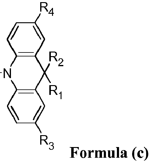
- X is an optionally substituted 9,9-disubstituted-9,10-dihydroacridine corresponding to the formula (c) wherein R 1 , R 2 , R 3 and R 4 are as previously defined.
- Ar is a substituted or unsubstituted aryl or heteroaryl group, said group being derived from a compound selected from the list consisting of dibenzo[b,d]furan, dibenzo[b,d]thiophene, carbazole, fluorene, benzene, naphthalene, anthracene and phenanthrene, which compounds may be substituted or unsubstituted.
- Ar is derived from dibenzo[b,d]thiophene, carbazole, fluorene or benzene, which compounds may be substituted or unsubstituted.
- Ar is derived from dibenzo[b,d]thiophene or benzene, which compounds may be substituted or unsubstituted.
- Ar is derived from substituted or unsubstituted dibenzo[b,d]thiophene.
- R 1 and R 2 which may be the same or different, are preferably selected among alkyl groups which may be linear, branched or cyclic and among optionally substituted phenyl groups. When substituted, phenyl groups are substituted with at least one substituent X as above defined.
- R 1 and R 2 are alkyl groups which may be linear, branched or cyclic.
- R 1 and R 2 are methyl groups.
- R 1 and R 2 form together, an optionally substituted cyclic moiety.
- R 1 and R 2 form together an optionally substituted heterofluorenyl or fluorenyl moiety.
- R 1 and R 2 form together an heterofluorenyl or a fluorenyl moiety which is substituted by at least one substituent X as previously described.
- R 1 and R 2 form together a fluorenyl moiety which is substituted by at least one substituent X as previously described.
- R 1 and R 2 form together a fluorenyl moiety which is substituted in position 3 and 6 by a substituent X as previously described; the case being the compound bearing at least one optionally substituted 9-R 1 -9-R 2 -9,10-dihydroacridine moiety according to the preferred embodiment E*, is represented in the formula (d) below wherein Ar, R 3 , R 4 and X are as herein defined.
- R 3 and R 4 independently from each other, are H or derived from a compound selected from the list of compounds comprising carbazole, dibenzothiophene, dibenzofuran and 9,9-disubstituted-9,10-dihydroacridine, which compounds may be substituted or unsubstituted with at least one substituent X as above defined.
- R 3 and R 4 independently from each other, are H or carbazole, which carbazole may be unsubstituted or unsubstituted with at least one substituent X as above defined.
- R 3 and R 4 are H or unsubstituted carbazole.
- R 3 and R 4 are H or R 3 and R 4 are unsubstituted carbazole.
- Ar is derived from substituted or unsubstituted dibenzo[b,d]thiophene and is thus an optionally substituted dibenzo[b,d]thiophenyl group; it is preferably an optionally substituted dibenzo[b,d]thiophen-2-yl.
- Ar is more preferably a dibenzo[b,d]thiophen-2-yl which is substituted with at least one substituent X as previously defined.
- Ar is even more preferably a dibenzo[b,d]thiophen-2-yl which is substituted in position 8 with a substituent X as previously defined; the case being, a representation of the compound bearing at least one optionally substituted 9-R 1 -9-R 2 -9,10-dihydroacridine moiety according to the preferred embodiment E1 is provided by formula (e) wherein R 1 , R 2 , R 3 , R 4 and X are as defined above.
- X is advantageously an optionally substituted 9,9-disubstituted-9,10-dihydroacridine corresponding to the formula (c); the case being, a representation of the compound bearing at least one optionally substituted 9-R 1 -9-R 2 -9,10-dihydroacridine moiety according to the preferred embodiment E1 is provided by formula (f) wherein R 1 , R 2 , R 3 and R 4 are as defined above.
- R 1 and R 2 are preferably methyl groups and R 3 and R 4 are preferably hydrogen atoms; the case being, a representation of the compound bearing at least one optionally substituted 9-R 1 -9-R 2 -9,10-dihydroacridine moiety according to the preferred embodiment E1 is provided by formula (g)
- Ar is derived from substituted or unsubstituted carbazole and is thus an optionally substituted carbazolyl group; it is preferably an optionally substituted carbazol-3-yl.
- Ar is more preferably a carbazol-3-yl which is substituted with at least one substituent X as previously defined.
- Ar is even more preferably a carbazol-3-yl which is substituted in position 6 with a substituent X as previously defined; the case being, a representation of the compound bearing at least one optionally substituted 9-R 1 -9-R 2 -9,10-dihydroacridine moiety according to the preferred embodiment E2 is provided by formula (h) wherein R, R 1 , R 2 , R 3 , R 4 and X are as defined above.
- Ar is derived from substituted or unsubstituted fluorene and is thus an optionally substituted fluorenyl group; it is preferably an optionally substituted fluorene-3-yl.
- Ar is more preferably a fluorene-3-yl which is substituted with at least one substituent X as previously defined.
- Ar is even more preferably a fluorene-3-yl which is substituted in position 6 with a substituent X as previously defined; the case being, a representation of the compound bearing at least one optionally substituted 9-R 1 -9-R 2 -9,10-dihydroacridine moiety according to the preferred embodiment E3 is provided by formula (i) wherein R', R", R 1 , R 2 , R 3 , R 4 and X are as defined above.
- Ar is derived from substituted or unsubstituted benzene group and is thus an optionally substituted benzyl group.
- Ar is preferably a benzyl group which is substituted with at least one substituent X as previously defined.
- Ar is more preferably an unsubstituted benzyl; the case being, a representation of the compound bearing at least one optionally substituted 9-R 1 -9-R 2 -9,10-dihydroacridine moiety according to the preferred embodiment E4 is provided by formula (j) wherein R 1 , R 2 , R 3 and R 4 are as defined above.
- R 1 and R 2 are advantageously methyl groups and R 3 and R 4 are advantageously unsubstituted carbazole; the case being, a representation of the compound bearing at least one optionally substituted 9-R 1 -9-R 2 -9,10-dihydroacridine moiety according to the preferred embodiment E4 is provided by formula (k)
- the at least one compound bearing at least one optionally substituted 9-R 1 -9-R 2 -9,10-dihydroacridine moiety is advantageously used as binder.
- Non exhaustive examples of compounds bearing at least one optionally substituted 9-R 1 -9-R 2 -9,10-dihydroacridine moiety particularly well suited to be used in the composition of the present invention are represented by formulae (I) to (XXV) below. Binders 1 to 2 represented below are even more particularly well suited to be used in the composition of the present invention.
- the compound bearing at least one optionally substituted 9-R 1 -9-R 2 -9,10-dihydroacridine moiety in accordance with the invention is advantageously amorphous. It exhibits advantageously a glass transition temperature of at least 80°C, preferably of at least 100°C and even more preferably of at least 120°C.
- the compound bearing at least one optionally substituted 9-R 1 -9-R 2 -9,10-dihydroacridine moiety contained in the compositions of the present invention has a HOMO level of less than -5.0 eV, preferably less than -5.2 eV and most preferably a HOMO level of less than -5.5 eV; besides, it has a LUMO level of more than -3.5 eV, preferably more than -3.3 eV and still more preferably more than -3.0 eV.
- composition in accordance with the invention comprises at least one crystalline organic semiconductor.
- crystalline is meant a compound that spontaneously self-organizes to give material which reveals a melting point that can be measured by any technique known by a person having ordinary skill in the art. For example, the presence of a melting point and its value can be determined by Differential Scanning Calorimetry.
- the crystalline organic semiconductor is chosen such that it exhibits a high tendency to crystallize when solution coating methods are used.
- the crystalline semiconductor is preferably a small molecule which has a molecular weight of 1600 Daltons or less, preferably 1200 Daltons or less, more preferably 1000 Daltons or less, even more preferably 800 Daltons or less.
- Preferred crystalline organic semiconducting materials which can be used in the present invention have a field effect mobility of at least 0.01 cm 2 /Vs, preferably of at least 0.1 cm 2 /Vs, more preferably of at least 1cm 2 /Vs.
- Crystalline organic semiconductors having suitable structures can be found in the review of Daoben Zhu et al. in Chemical Reviews, 2012, 112, 2208-2267 and more particularly in Table 2 of the said review.
- Exemplary small molecule organic semiconductors are selected from compounds of formulae: wherein Ar 1 to Ar 7 are the same or different at each occurrence and are each independently selected from the group consisting of monocyclic aromatic rings and monocyclic heteroaryl aromatic rings, with at least one of Ar 1 to Ar 7 being substituted with at least one substituent Z which may be the same or different at each occurrence and is selected from the group consisting of unsubstituted or substituted straight, branched or cyclic alkyl groups having from 1 to 50 carbon atoms, alkoxy groups having from 1 to 50 carbon atoms, aryloxy groups having from 6 to 40 carbon atoms, alkylaryloxy groups having from 7 to 40 carbon atoms, alkoxycarbonyl groups having from 2 to 40 carbon atoms, aryloxycarbonyl groups having from 7 to 40 carbon atoms, amino groups that may be unsubstituted or substituted with one or two alkyl groups having from 1 to 20 carbon atoms, each of which may be the same or different, amido
- At least one of Ar 1 to Ar 7 comprises a 5 to 7 membered heteroaryl group containing from 1 to 3 sulfur atoms, oxygen atoms, selenium atoms and/or nitrogen atoms.
- Ar 1 to Ar 7 are independently selected from phenyl and thiophene and at least one of Ar 1 to Ar 7 is thiophene.
- a first group of small molecule organic semiconductors in accordance with the above general formulae which can be used in the compositions of the present invention are oligo- and polyacenes.
- Acenes or polyacenes are a class of organic compounds and parties cyclic aromatic hydrocarbons made up of linearly fused benzene rings, i.e. having a skeleton of general formula which may be substituted with substituents Z as defined above in any position.
- n is an integer in the range of from 1 to 4.
- Pentacene compounds for which n is 3 and corresponding to formula (3) have been used in a number of applications for the manufacture of organic electronic devices.
- Exemplary representatives of suitable pentacene compounds are represented by formulae below: in which Z', which may be the same or different at each occurrence, is hydrogen or has a meaning as defined above for Z, with the proviso that at least one substituent Z' is different from hydrogen, and wherein A is carbon, silicon or germanium, preferably silicon or germanium.
- the substituents Z' at the atom A in this case are preferably alkyl groups or alkoxy groups having from 1 to 20, preferably from 1 to 12 and even more preferably 1 to 8 carbon atoms.
- Still another group of compounds corresponding to formula (3) is represented by formula wherein again Z' and A are as defined above and may be the same or different at each occurrence and wherein W is selected from the group consisting of S, NH, NZ' or Se, preferably from S or Se.
- the substituents Z' at the atom A in this case are preferably alkyl groups or alkoxy groups having from 1 to 20, more preferably from 1 to 12 and even more preferably from 1 to 8 carbon atoms and the substituent Z' in NZ' is an alkyl group having from 1 to 12, more preferably from 1 to 8 carbon atoms.
- Another group of compounds of general formula (2) preferred as organic semiconductors in the present invention are compounds of general formula wherein W is as defined above and which may bear substituents Z' as defined above at any of the carbon atoms of the ring system.
- Another group of compounds of general formula (4) preferred as organic semiconductors in the present invention are compounds of general formula wherein W is as defined above and which may bear substituents Z' as defined above at any of the carbon atoms of the ring system.
- Another group of compounds of general formula (5) preferred as organic semiconductors in the present invention are compounds of general formula wherein W is as defined above and which may bear substituents Z' as defined above at any of the carbon atoms of the ring system.
- Still another group of preferred organic semiconductors in the compositions of the present invention and corresponding to formula (3) are furan or thiophene V-shaped organic semiconducting materials of general formula wherein T is an oxygen or a sulfur atom and Z', which may be the same or different at each occurence, may have the meaning as defined above.
- T is preferably sulfur
- Still another group of preferred organic semiconductors in the compositions of the present invention and corresponding to formula (1) is V-shaped organic semiconducting materials of general formula which may bear substituents Z' as defined above at any of the carbon atoms of the ring system.
- a preferred organic semiconductor corresponding to a general formula (B) is represented by formula
- R which may be the same or different, represents an alkyl group having 1 to 30, preferably from 1 to 20 and most preferably from 1 to 12 carbon atoms.
- R represents an alkyl group having 1 to 30, preferably from 1 to 20 and most preferably from 1 to 12 carbon atoms.
- a particularly preferred compound of this group is known as C8-BTBT in which both substituents R" are n-C 8 H 17 (n-octyl) groups.
- R represents an alkyl group having 1 to 30, preferably from 1 to 20 and most preferably from 1 to 12 carbon atoms.
- R represents an alkyl group having 1 to 30, preferably from 1 to 20 and most preferably from 1 to 12 carbon atoms.
- a particularly preferred compound of this group is known as C10-DNBDT in which both substituents R" are n-C 10 H 21 groups.
- the weight ratio of crystalline organic semiconductor to the compound bearing at least one optionally substituted 9-R 1 -9-R 2 -9,10-dihydroacridine moiety is comprised from 5/95 to 95/5, preferably from 25/75 to 75/25, more preferably from 34/66 to 66/34.
- composition according to the invention may be available in the form of an ink, i.e. it further comprises at least one organic solvent, which form makes it easily deposited onto a substrate.
- the combined content of the compound bearing at least one optionally substituted 9-R 1 -9-R 2 -9,10-dihydroacridine moiety and of the crystalline organic semiconductor versus the total weight of the composition is of at least 0.5 wt %, preferably of at least 1 wt % and more preferably of at least 1.5 wt %; besides, the combined content of the compound bearing at least one optionally substituted 9-R 1 -9-R 2 -9,10-dihydroacridine moiety and of the crystalline organic semiconductor versus the total weight of the composition (i.e. including, inter alia, the organic solvent) is of at most 10 wt %, preferably of at most 5 wt % and more preferably of at most 3 wt %, with regard to the total weigh of the composition.
- the composition is coated onto a substrate by vacuum deposition. Then, it is advantageously free of solvent.
- the solvent comprised in the ink is advantageously removed from the composition after the ink is deposited on the substrate, thereby obtaining advantageously a composition essentially free or even completely free of solvent.
- an organic solvent may be present or not.
- the weight content of the compound bearing at least one optionally substituted 9-R 1 -9-R 2 -9,10-dihydroacridine moiety is generally of at least 5 wt. % with regard to the total weight of the composition diminished by the weight of the organic solvent, whatever present or not. It is preferably of at least 25 wt. %, more preferably of at least 35 wt. %, even more preferably of at least 50 wt. % with regard to the total weight of the composition diminished by the weight of the organic solvent.
- the weight content of the compound bearing at least one optionally substituted 9-R 1 -9-R 2 -9,10-dihydroacridine moiety is generally of at most 95 wt.
- % with regard to the total weight of the composition diminished by the weight of the organic solvent; it is preferably of at most 85 wt. %, more preferably of at most 75 wt. %, even more preferably of at most 65 wt. % with regard to the total weight of the composition diminished by the weight of the organic solvent.
- the viscosity of the solvents preferably is in the range of from 0.2 to 50 mPa.s, preferably in the range of from 1 to 20 mPa.s, measured at 25°C.
- Hansen solubility parameters of the solvent used are preferably within the following ranges:
- the solvent surface tension in mN/m (at 20°C) is preferably in the range of from 10 to 70, more preferably in the range of from 20 to 50 and most preferably in the range of from 26 to 38.
- suitable and preferred organic solvents include, without being limited to, dichloromethane, trichloromethane, monochlorobenzene, o-dichlorobenzene, the respective bromobenzenes, tetrahydrofuran, anisole, morpholine, toluene, o-xylene, m-xylene, p-xylene, the isomeric trimethylbenzenes, in particular 1,3,5 trimethylbenzene (also known as mesitylene), 1,4-dioxane, acetone, 1,1,2,2-tetrachloroethane, ethyl acetate, n-butyl acetate, dimethylformamide, dimethylacetamide, dimethylsulfoxide, tetralin (tetrahydronaphthalene), halogenated naphthalenes, such as 1-bromo naphthalene, decalin, indane and/or mixtures thereof.
- Especially preferred solvents for use in the compositions according to the present invention are anisole, the isomeric xylenes, toluene, mesitylene, tetralin, chlorobenzene, bromobenzene, o-dichlorobenzene and 1-bromonaphthalin and/or mixtures thereof.
- the preferred solvents have a boiling point in the range of from 80 to 350, preferably of from 100 to 300 and even more preferably of from 130 to 230°C.
- composition in accordance with the present invention can additionally comprise one or more further components like e.g. surface-active compounds, lubricating agents, wetting agents, dispersing agents, hydrophobic agents, adhesive agents, flow improvers, defoaming agents, deaerators, diluents (reactive or non-reactive), auxiliaries, colorants, dyes, pigments or nanoparticles.
- further components like e.g. surface-active compounds, lubricating agents, wetting agents, dispersing agents, hydrophobic agents, adhesive agents, flow improvers, defoaming agents, deaerators, diluents (reactive or non-reactive), auxiliaries, colorants, dyes, pigments or nanoparticles.
- the semiconducting layer obtained through the use of the composition in accordance with the present invention is typically at most 1 ⁇ m thick, preferably at most 500 nm although greater thicknesses may be achieved if required.
- the semiconducting layer obtained is typically at least 10 nm thick, preferably at least 50 nm.
- the present invention also relates to a process for the manufacture of an organic semiconducting layer comprising applying the composition as above described to form a layer onto a substrate.
- the composition additionally comprises at least one organic solvent and the process further comprises evaporating the solvent from the layer.
- composition in accordance with the present invention enables the use of numbers of liquid coating techniques.
- dip coating spin coating, slot die coating, inkjet printing, letter-press printing, screen printing, doctor blade coating, roller printing, reverse roller-printing, offset lithography printing, flexographic printing, flexographic coating, spray coating, brush coating or pad printing may be mentioned here.
- the inkjet fluid i.e. the mixture of semiconducting compounds, binder and solvent
- the inkjet fluid preferably has a viscosity at 20°C of 1-100 mPa.s, more preferably of 1-50 mPa.s and most preferably 1-30 mPa.s.
- a substrate used for preparing the organic semiconducting layer may include any underlying device layer, electrode or separate substrate such as e.g. silicon wafer, glass or polymer substrate.
- the present invention furthermore relates to an organic electronic device comprising an organic semiconducting layer in accordance with the invention.
- the electronic device generally comprises a gate electrode, a source electrode and a drain electrode, said device further comprises an organic semiconducting layer between the source and drain electrode, which organic semiconducting layer is obtained using the composition in accordance with the present invention.
- Preferred organic electronic devices are organic field effect transistors.
- the present invention finally relates to an electronic device comprising an organic field effect transistor comprising a semiconducting layer obtained using the composition in accordance with the invention.
- the said electronic device is generally a display, more preferably an active matrix display, even more preferably an active matrix OLED display.
- OFTs Organic Thin Film Transistors
- 1" square glass substrates (ex: Corning XG) were cleaned using sonication bathes for 5 minutes in Deconex (3% in water) followed by rinsing in ultrapure water and dried using compressed air.
- a planarization layer was first spin coated on top of the cleaned substrates in order to create a 30 nm film after photocrosslinking.
- Au (30 nm) bottom contact source/drain (S/D) electrodes were deposited on top of the planarization layer by thermal evaporation through a shadow mask.
- the 16 transistors S/D consisted of electrodes with channel length of 50 ⁇ m and channel width of 0.5mm.
- the substrates then underwent UV/O 3 treatment (model 42-220, from Jelight Company, Inc.), treatment time 5min.
- OSC organic semiconductor
- the organic semiconductor (OSC) formulation was spin coated onto the SD electrodes using a Laurell spinner set at 1500 rpm followed by baking on a hotplate for 60 seconds at 100°C.
- Hyflon ® AD SF (9.2% w/w) solution commercialized by Solvay Specialty Polymers was spin coated at 3000 rpm and the samples were baked on a hotplate for 60s at 100°C.
- Gate electrodes were defined by evaporation of Aluminum (60nm) through a shadow mask in a thermal evaporator system.
- OTFTs were tested using a Cascade Microtech EP6 DC probe station in conjunction with an Agilent B1500A semiconductor parameter analyzer.
- the mobility values reported are an average of the 5 highest points in accumulation for each transistor. The standard deviation of the mobility values is reported as a percentage of the mean.
- the OTFT array fabricated and characterized as the comparative example 1 was fabricated and tested as described above.
- the formulation tested in the comparative example 1 included small molecule semiconductor however this formulation did not incorporate any binder.
- 1,4,8,1 1-tetramethyl-6,13-triethylsilylethynylpentacene represented by formula ( OS1 ) was formulated in tetralin at 1.5% by weight total solids content. This was coated as an OSC layer in an OTFT device according to the method shown above for glass substrate.
- ⁇ Lin 1.8 ⁇ 0.8 cm 2 / Vs ; standard deviation as a % of the mean value of the mobility was 44.4 % .
- the OTFT array fabricated and characterized as the comparative example 2 was fabricated and tested as described above.
- the formulation tested in the comparative example 2 included a small molecule semiconductor and a triarylamine polymer as binder.
- 1,4,8,1 1-tetramethyl-6,13-triethylsilylethynylpentacene represented by formula ( OS1 ) and Poly[bis(4-phenyl)(2,4,6-trimethylphenyl)amine] were formulated in tetralin in a ratio 50:50 at total solids content of 2% by weight. This was coated as an OSC layer in an OTFT device according to the method shown above for glass substrate.
- ⁇ Lin 3.8 ⁇ 1.1 cm 2 / Vs ; standard deviation as a % of the mean value of the mobility was 28.9 % .
- the OTFT arrays fabricated and characterized as the examples 1 to 2 were fabricated and tested as described above.
- the formulations tested in the examples 1 to 2 included small molecule semiconductor and an amorphous small-molecule as binder. In these examples the ratio of binder to the semiconductor is in parts by weight.
- Example 1 1,4,8,11-tetramethyl-6,13-Triethylsilylethynylpentacene with small-molecule bearing at least one optionally substituted 9-R 1 -9-R 2 -9,10-dihydroacridine moiety as the binder; TG OTFT 2,8-bis(9,9-dimethylacridin-10(9H)-yl)dibenzo[b,d]thiophene (Binder 1), was formulated with 1,4,8,1 1-tetramethyl-6,13-triethylsilylethynyl pentacene represented by formula ( OS1 ) in a ratio 60:40 at a total solids content of 1.5% by weight in tetralin and coated as an OSC layer in an OTFT device according to the method shown above for glass substrate devices.
- OS1 1,4,8,11-tetramethyl-6,13-Triethylsilylethynylpentacene with small-molecule bearing
- ⁇ Lin 5.3 ⁇ 0.5 cm 2 / Vs ; standard deviation as a % of the mean value of the mobility was 9.4 % .
- Example 2 1,4,8,11 -tetramethyl-6,13-Triethylsilylethynylpentacene with small-molecule bearing at least one optionally substituted 9-R 1 -9-R 2 -9,10-dihydroacridine moiety as the binder; TG OTFT 2,7-di(9H-carbazol-9-yl)-9,9-dimethyl-10-phenyl-9,10-dihydroacridine (Binder 2), was formulated with 1,4,8,11-tetramethyl-6,13-Triethylsilylethynylpentacene represented by formula ( OS1 ) in a ratio 60:40 at a total solids content of 1.5% by weight in tetralin and coated as an OSC layer in an OTFT device according to the method shown above for glass substrate devices.
- OS1 1,4,8,11 -tetramethyl-6,13-Triethylsilylethynylpentacen
- ⁇ Lin 4.8 ⁇ 0.4 cm 2 / Vs ; standard deviation as a % of the mean value of the mobility was 8.5 % .
- composition in accordance with the present invention comprising an organic semiconductor and a small molecule bearing at least one optionally substituted 9-R 1 -9-R 2 -9,10-dihydroacridine moiety as the binder yielded OTFTs with improved performance compared to OTFTs obtained using compositions in accordance with the prior art. More particularly, measured linear mobility values were high, the standard deviation of the mobility values was low and the bias stress stability was improved.
Landscapes
- Engineering & Computer Science (AREA)
- Chemical & Material Sciences (AREA)
- Materials Engineering (AREA)
- Physics & Mathematics (AREA)
- Spectroscopy & Molecular Physics (AREA)
- Composite Materials (AREA)
- Manufacturing & Machinery (AREA)
- Thin Film Transistor (AREA)
- Heterocyclic Carbon Compounds Containing A Hetero Ring Having Oxygen Or Sulfur (AREA)
Abstract

Description
- The present invention concerns an organic semiconductor composition comprising an organic crystalline semiconductor and at least one compound bearing at least one optionally substituted 9,9-disubstituted-9,10-dihydroacridine moiety and the use thereof for the manufacture of organic semiconducting layers suitable for the manufacture of organic electronic devices.
- Organic semiconducting layers have been the object of many attentions in the field of organic electronics. Especially when low cost organic electronics devices are targeted, one needs cheap material, easy processes and high cadences to produce the devices. Process to manufacture organic semiconducting thin layers may involve deposition under vacuum or may involve a solution process like ink printing. Liquid coating of organic semiconductor (OSC) composition is generally preferred over vacuum deposition techniques. The use of crystalline semiconductor such as TIPS-pentacene alone in a semiconducting layer may require drastic conditions and long times to promote convenient crystallization both being detrimental to manufacture with high cadences. Moreover, crystallization of any crystalline OSC alone is such a sensitive process that reproducibility may be impaired by minor changes during manufacturing.
-
DE102010061978 and J. Appl. Phys. 100, 023716 (2006) disclose the use of acridine orange base (AOB) as dopant for n-type organic semiconductors (n-type OSC) such as fluorocarbon-substituted dicyanoperylene-3,4:9,10-bis(dicarboximide) (PDIF-CN2) and C60 in a semiconducting layer of an organic field effect transistor (OFET). For this purpose, in order to be able to provide electron doping, AOB has a HOMO level which is higher than the LUMO level of n-type OSC. Field effect mobility measured for a device prepared in the presence of a small amount of dopant is generally higher than the mobility measured for a device prepared without dopant. However, with too high doping ratios the crystalline order of the semiconductor is disturbed and properties are reduced. -
US2009165848 relates to organic electronic devices, which may be OFET, using quinacridine derivatives. In this patent application, quinacridine derivatives are used as crystalline OSC for OFET application and resulting devices have low performances. Moreover, the crystalline OSC is used alone in the semiconducting layer of the OFET, which may impair the stability and the reproducibility because of crystallization processes highly sensitive to experimental conditions. - There is a need for a new organic semiconductor composition suitable for preparing a semiconducting layer of an electronic device having reproducible properties, in particular reproducible high field effect mobility.
- There is also a need for an organic semiconducting layer having high stability and, more particularly, bias stress stability.
- There is also a need for an organic semiconductor composition suitable for preparing semiconducting layer having high field effect mobility, low cost and easy processing.
- The needs previously described and others, are advantageously met by a composition comprising at least one crystalline organic semiconductor and at least one compound bearing at least one optionally substituted 9,9-disubstituted-9,10-dihydroacridine moiety, said compound corresponding to formula (a)


- R1 and R2, which may be the same or different, represent a C1-C50 hydrocarbyl or heterohydrocarbyl group, optionally forming together an optionally substituted cyclic moiety,
- R3 and R4, which may be the same or different, represent H or a C1-C24 hydrocarbyl or heterohydrocarbyl group, and
- Ar is an optionally substituted aryl or heteroaryl group.
- The term "hydrocarbyl" as used herein refers to a group only containing carbon and hydrogen atoms. The hydrocarbyl group may be saturated or unsaturated, linear, branched or cyclic. If the hydrocarbyl is cyclic, the cyclic group may be an aromatic or non-aromatic group.
- The term "heterohydrocarbyl" as used herein refers to a hydrocarbyl group wherein one or more of the carbon atom(s) is/are replaced by a heteroatom, such as Si, S, N or O. Included within this definition are heteroaromatic rings, i.e. wherein one or more carbon atom within the ring structure of an aromatic ring is replaced by a heteroatom.
- Ar is generally a substituted or unsubstituted aryl or a substituted or unsubstituted heteroaryl group, said aryl or heteroaryl group being derived from a compound selected from the list of compounds of following formulae:


- By aryl or heteroaryl group derived from a compound comprising at least one aromatic or heteroaromatic ring, is meant an aryl or heteroaryl group that can be obtained by the removal of one hydrogen atom from the aromatic or heteroaromatic ring of the compound. For example, dibenzo[b,d]thiophen-2-yl can be obtained by removing the hydrogen atom in the position 2 of dibenzo[b,d]thiophene. Thus in the meaning of the present invention, dibenzothiophen-2-yl is an aryl group derived from dibenzothiophene.

- Ar may be substituted on any carbon atom by a substituent X, wherein X, which may be the same or different at each occurrence, represents H , -NR5R6, or a C1-C30 hydrocarbyl or heterohydrocarbyl group, wherein R5 and R6, which may be similar or different, are a phenyl group optionally substituted by a C1-C30 hydrocarbyl or heterohydrocarbyl group.
- The said C1-C30 hydrocarbyl or heterohydrocarbyl group is preferably derived from an optionally substituted compound selected among the list comprising carbazole, dibenzothiophene, dibenzofuran and 9,9-disubstituted-9,10-dihydroacridine.
- In a preferred embodiment, X is an optionally substituted 9,9-disubstituted-9,10-dihydroacridine corresponding to the formula (c)
- Advantageously, Ar is a substituted or unsubstituted aryl or heteroaryl group, said group being derived from a compound selected from the list consisting of dibenzo[b,d]furan, dibenzo[b,d]thiophene, carbazole, fluorene, benzene, naphthalene, anthracene and phenanthrene, which compounds may be substituted or unsubstituted.
- Preferably, Ar is derived from dibenzo[b,d]thiophene, carbazole, fluorene or benzene, which compounds may be substituted or unsubstituted.
- More preferably, Ar is derived from dibenzo[b,d]thiophene or benzene, which compounds may be substituted or unsubstituted.
- Even more preferably, Ar is derived from substituted or unsubstituted dibenzo[b,d]thiophene.
- R1 and R2, which may be the same or different, are preferably selected among alkyl groups which may be linear, branched or cyclic and among optionally substituted phenyl groups. When substituted, phenyl groups are substituted with at least one substituent X as above defined.
- More preferably, R1 and R2 are alkyl groups which may be linear, branched or cyclic.
- Even more preferably R1 and R2 are methyl groups.
- In a particular embodiment E*, R1 and R2 form together, an optionally substituted cyclic moiety. In embodiment E*, R1 and R2 form together an optionally substituted heterofluorenyl or fluorenyl moiety. In embodiment E*, more preferably, R1 and R2 form together an heterofluorenyl or a fluorenyl moiety which is substituted by at least one substituent X as previously described. In embodiment E*, still more preferably, R1 and R2 form together a fluorenyl moiety which is substituted by at least one substituent X as previously described. In embodiment E*, the most preferably, R1 and R2 form together a fluorenyl moiety which is substituted in position 3 and 6 by a substituent X as previously described; the case being the compound bearing at least one optionally substituted 9-R1-9-R2-9,10-dihydroacridine moiety according to the preferred embodiment E*, is represented in the formula (d) below

- Preferably, R3 and R4, independently from each other, are H or derived from a compound selected from the list of compounds comprising carbazole, dibenzothiophene, dibenzofuran and 9,9-disubstituted-9,10-dihydroacridine, which compounds may be substituted or unsubstituted with at least one substituent X as above defined.
- More preferably, R3 and R4, independently from each other, are H or carbazole, which carbazole may be unsubstituted or unsubstituted with at least one substituent X as above defined.
- Still more preferably, R3 and R4 are H or unsubstituted carbazole.
- The most preferably, either R3 and R4 are H or R3 and R4 are unsubstituted carbazole.
- In a preferred embodiment E1, Ar is derived from substituted or unsubstituted dibenzo[b,d]thiophene and is thus an optionally substituted dibenzo[b,d]thiophenyl group; it is preferably an optionally substituted dibenzo[b,d]thiophen-2-yl.
- Ar is more preferably a dibenzo[b,d]thiophen-2-yl which is substituted with at least one substituent X as previously defined.
- Ar is even more preferably a dibenzo[b,d]thiophen-2-yl which is substituted in position 8 with a substituent X as previously defined; the case being, a representation of the compound bearing at least one optionally substituted 9-R1-9-R2-9,10-dihydroacridine moiety according to the preferred embodiment E1 is provided by formula (e)

- In accordance with embodiment E1, X is advantageously an optionally substituted 9,9-disubstituted-9,10-dihydroacridine corresponding to the formula (c); the case being, a representation of the compound bearing at least one optionally substituted 9-R1-9-R2-9,10-dihydroacridine moiety according to the preferred embodiment E1 is provided by formula (f)

- In accordance with embodiment E1, R1 and R2 are preferably methyl groups and R3 and R4 are preferably hydrogen atoms; the case being, a representation of the compound bearing at least one optionally substituted 9-R1-9-R2-9,10-dihydroacridine moiety according to the preferred embodiment E1 is provided by formula (g)

- In a preferred embodiment E2, Ar is derived from substituted or unsubstituted carbazole and is thus an optionally substituted carbazolyl group; it is preferably an optionally substituted carbazol-3-yl.
Ar is more preferably a carbazol-3-yl which is substituted with at least one substituent X as previously defined. - Ar is even more preferably a carbazol-3-yl which is substituted in position 6 with a substituent X as previously defined; the case being, a representation of the compound bearing at least one optionally substituted 9-R1-9-R2-9,10-dihydroacridine moiety according to the preferred embodiment E2 is provided by formula (h)

- In a preferred embodiment E3, Ar is derived from substituted or unsubstituted fluorene and is thus an optionally substituted fluorenyl group; it is preferably an optionally substituted fluorene-3-yl.
- Ar is more preferably a fluorene-3-yl which is substituted with at least one substituent X as previously defined.
- Ar is even more preferably a fluorene-3-yl which is substituted in position 6 with a substituent X as previously defined; the case being, a representation of the compound bearing at least one optionally substituted 9-R1-9-R2-9,10-dihydroacridine moiety according to the preferred embodiment E3 is provided by formula (i)

- In a preferred embodiment E4, Ar is derived from substituted or unsubstituted benzene group and is thus an optionally substituted benzyl group.
- Ar is preferably a benzyl group which is substituted with at least one substituent X as previously defined.
- Ar is more preferably an unsubstituted benzyl; the case being, a representation of the compound bearing at least one optionally substituted 9-R1-9-R2-9,10-dihydroacridine moiety according to the preferred embodiment E4 is provided by formula (j)

- In accordance with embodiment E4, R1 and R2 are advantageously methyl groups and R3 and R4 are advantageously unsubstituted carbazole; the case being, a representation of the compound bearing at least one optionally substituted 9-R1-9-R2-9,10-dihydroacridine moiety according to the preferred embodiment E4 is provided by formula (k)

- In the composition according to the invention, the at least one compound bearing at least one optionally substituted 9-R1-9-R2-9,10-dihydroacridine moiety is advantageously used as binder.
- Non exhaustive examples of compounds bearing at least one optionally substituted 9-R1-9-R2-9,10-dihydroacridine moiety particularly well suited to be used in the composition of the present invention are represented by formulae (I) to (XXV) below. Binders 1 to 2 represented below are even more particularly well suited to be used in the composition of the present invention.


- The compound bearing at least one optionally substituted 9-R1-9-R2-9,10-dihydroacridine moiety in accordance with the invention is advantageously amorphous. It exhibits advantageously a glass transition temperature of at least 80°C, preferably of at least 100°C and even more preferably of at least 120°C.
- It has been advantageous, in certain circumstances, that the compound bearing at least one optionally substituted 9-R1-9-R2-9,10-dihydroacridine moiety contained in the compositions of the present invention has a HOMO level of less than -5.0 eV, preferably less than -5.2 eV and most preferably a HOMO level of less than -5.5 eV; besides, it has a LUMO level of more than -3.5 eV, preferably more than -3.3 eV and still more preferably more than -3.0 eV.
- The composition in accordance with the invention comprises at least one crystalline organic semiconductor. By crystalline, is meant a compound that spontaneously self-organizes to give material which reveals a melting point that can be measured by any technique known by a person having ordinary skill in the art. For example, the presence of a melting point and its value can be determined by Differential Scanning Calorimetry. The crystalline organic semiconductor is chosen such that it exhibits a high tendency to crystallize when solution coating methods are used.
- The crystalline semiconductor is preferably a small molecule which has a molecular weight of 1600 Daltons or less, preferably 1200 Daltons or less, more preferably 1000 Daltons or less, even more preferably 800 Daltons or less.
- Preferred crystalline organic semiconducting materials which can be used in the present invention have a field effect mobility of at least 0.01 cm2/Vs, preferably of at least 0.1 cm2/Vs, more preferably of at least 1cm2/Vs. The mobility referred to here is preferably determined in the saturation mode using a field effect transistor. In this technique, for each fixed gate voltage VGS the drain-source voltage VDS is increased until the current Io saturates. Next, the square root of this saturated current is plotted against the gate voltage and the slope msat is measured. Then the mobility is

- There is no limitation in the choice of the structure of the crystalline organic semiconductor that can be used in the present invention. The person skilled in the art can select the crystalline organic semiconductor based on his professional knowledge and based on some reviews on the subject. Crystalline organic semiconductors having suitable structures can be found in the review of Daoben Zhu et al. in Chemical Reviews, 2012, 112, 2208-2267 and more particularly in Table 2 of the said review.
- Exemplary small molecule organic semiconductors are selected from compounds of formulae:


- In accordance with a preferred embodiment at least one of Ar1 to Ar7 comprises a 5 to 7 membered heteroaryl group containing from 1 to 3 sulfur atoms, oxygen atoms, selenium atoms and/or nitrogen atoms.
- In a still further embodiment Ar1 to Ar7 are independently selected from phenyl and thiophene and at least one of Ar1 to Ar7 is thiophene.
- A first group of small molecule organic semiconductors in accordance with the above general formulae which can be used in the compositions of the present invention are oligo- and polyacenes.
- Acenes or polyacenes are a class of organic compounds and parties cyclic aromatic hydrocarbons made up of linearly fused benzene rings, i.e. having a skeleton of general formula

- Pentacene compounds for which n is 3 and corresponding to formula (3) have been used in a number of applications for the manufacture of organic electronic devices. Exemplary representatives of suitable pentacene compounds are represented by formulae below:


- Still another group of compounds corresponding to formula (3) is represented by formula

- Another group of compounds of general formula (2) preferred as organic semiconductors in the present invention are compounds of general formula

- Another group of compounds of general formula (4) preferred as organic semiconductors in the present invention are compounds of general formula

- Another group of compounds of general formula (5) preferred as organic semiconductors in the present invention are compounds of general formula

- Still another group of preferred organic semiconductors in the compositions of the present invention and corresponding to formula (3) are furan or thiophene V-shaped organic semiconducting materials of general formula

- Representative examples are

- Compounds of this structure as well as their synthesis have been described in Adv. Mater. 2013, 25, 6392-6397 and Chem. Comm. 2014, 50, 5342-5344 to which reference is made for further details.
- Still another group of preferred organic semiconductors in the compositions of the present invention and corresponding to formula (1) is V-shaped organic semiconducting materials of general formula

- Representative examples are

- Compounds of this structure as well as their synthesis have been described in Chem. Comm. 2013, 49, 6483-6485 to which reference is made for further details.
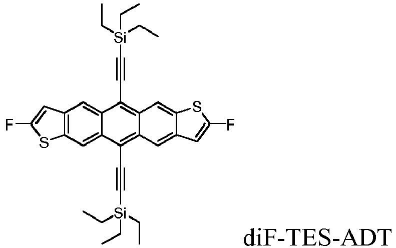
- Particularly preferred examples for compounds of formula (A) are the compounds of formulae below which are generally known under the names given next to the formula

- A preferred organic semiconductor corresponding to a general formula (B) is represented by formula
- Particularly preferred representatives of general formula (C) are benzothieno benzothiophene derivatives represented by general formula below

- Particularly preferred representative of general formula (D) is Dinaphtothienothiophene derivative represented by general formula below

- Particularly preferred representatives of general formula (E) are derivatives represented by general formula below

- In the composition according to the invention, the weight ratio of crystalline organic semiconductor to the compound bearing at least one optionally substituted 9-R1-9-R2-9,10-dihydroacridine moiety is comprised from 5/95 to 95/5, preferably from 25/75 to 75/25, more preferably from 34/66 to 66/34.
- The composition according to the invention may be available in the form of an ink, i.e. it further comprises at least one organic solvent, which form makes it easily deposited onto a substrate.
- In such case the combined content of the compound bearing at least one optionally substituted 9-R1-9-R2-9,10-dihydroacridine moiety and of the crystalline organic semiconductor versus the total weight of the composition (i.e. including, inter alia, the organic solvent) is of at least 0.5 wt %, preferably of at least 1 wt % and more preferably of at least 1.5 wt %; besides, the combined content of the compound bearing at least one optionally substituted 9-R1-9-R2-9,10-dihydroacridine moiety and of the crystalline organic semiconductor versus the total weight of the composition (i.e. including, inter alia, the organic solvent) is of at most 10 wt %, preferably of at most 5 wt % and more preferably of at most 3 wt %, with regard to the total weigh of the composition.
- In particular embodiments, the composition is coated onto a substrate by vacuum deposition. Then, it is advantageously free of solvent. Besides, when the composition according to the invention is available in the form of an ink, the solvent comprised in the ink is advantageously removed from the composition after the ink is deposited on the substrate, thereby obtaining advantageously a composition essentially free or even completely free of solvent.
- Thus, in the invented composition, an organic solvent may be present or not.
- In any case, the weight content of the compound bearing at least one optionally substituted 9-R1-9-R2-9,10-dihydroacridine moiety is generally of at least 5 wt. % with regard to the total weight of the composition diminished by the weight of the organic solvent, whatever present or not. It is preferably of at least 25 wt. %, more preferably of at least 35 wt. %, even more preferably of at least 50 wt. % with regard to the total weight of the composition diminished by the weight of the organic solvent. Besides, the weight content of the compound bearing at least one optionally substituted 9-R1-9-R2-9,10-dihydroacridine moiety is generally of at most 95 wt. % with regard to the total weight of the composition diminished by the weight of the organic solvent; it is preferably of at most 85 wt. %, more preferably of at most 75 wt. %, even more preferably of at most 65 wt. % with regard to the total weight of the composition diminished by the weight of the organic solvent.
- The viscosity of the solvents preferably is in the range of from 0.2 to 50 mPa.s, preferably in the range of from 1 to 20 mPa.s, measured at 25°C.
- The Hansen solubility parameters of the solvent used, expressed in MPa1/2, are preferably within the following ranges:
- Hd: 15 to 25, preferably 17 to 23
- Hp: 0 to 20, preferably 0 to 15
- Hh: 0 to 25, preferably 0 to 20
- wherein Hd, Hp and Hh respectively represent the dispersive, the polar and the hydrogen bonding solubility parameters.
- The solvent surface tension in mN/m (at 20°C) is preferably in the range of from 10 to 70, more preferably in the range of from 20 to 50 and most preferably in the range of from 26 to 38.
- Examples of suitable and preferred organic solvents include, without being limited to, dichloromethane, trichloromethane, monochlorobenzene, o-dichlorobenzene, the respective bromobenzenes, tetrahydrofuran, anisole, morpholine, toluene, o-xylene, m-xylene, p-xylene, the isomeric trimethylbenzenes, in particular 1,3,5 trimethylbenzene (also known as mesitylene), 1,4-dioxane, acetone, 1,1,2,2-tetrachloroethane, ethyl acetate, n-butyl acetate, dimethylformamide, dimethylacetamide, dimethylsulfoxide, tetralin (tetrahydronaphthalene), halogenated naphthalenes, such as 1-bromo naphthalene, decalin, indane and/or mixtures thereof.
- Especially preferred solvents for use in the compositions according to the present invention are anisole, the isomeric xylenes, toluene, mesitylene, tetralin, chlorobenzene, bromobenzene, o-dichlorobenzene and 1-bromonaphthalin and/or mixtures thereof.
- Even more preferred solvents are anisole and tetralin.
- The preferred solvents have a boiling point in the range of from 80 to 350, preferably of from 100 to 300 and even more preferably of from 130 to 230°C.
- The composition in accordance with the present invention can additionally comprise one or more further components like e.g. surface-active compounds, lubricating agents, wetting agents, dispersing agents, hydrophobic agents, adhesive agents, flow improvers, defoaming agents, deaerators, diluents (reactive or non-reactive), auxiliaries, colorants, dyes, pigments or nanoparticles.
- It is also the object of the present invention to disclose the use of the composition in accordance with the present invention for the manufacture of a semiconducting layer.
- The semiconducting layer obtained through the use of the composition in accordance with the present invention is typically at most 1 µm thick, preferably at most 500 nm although greater thicknesses may be achieved if required. The semiconducting layer obtained is typically at least 10 nm thick, preferably at least 50 nm.
- The present invention also relates to a process for the manufacture of an organic semiconducting layer comprising applying the composition as above described to form a layer onto a substrate.
- Preferably, in the invented process, the composition additionally comprises at least one organic solvent and the process further comprises evaporating the solvent from the layer.
- Indeed to form a layer onto a substrate, especially a thin, layer, liquid coating of organic semiconductor composition is generally preferred over vacuum deposition which is possible anyway. The composition in accordance with the present invention enables the use of numbers of liquid coating techniques.
- Just by way of example dip coating, spin coating, slot die coating, inkjet printing, letter-press printing, screen printing, doctor blade coating, roller printing, reverse roller-printing, offset lithography printing, flexographic printing, flexographic coating, spray coating, brush coating or pad printing may be mentioned here.
- The inkjet fluid (i.e. the mixture of semiconducting compounds, binder and solvent) preferably has a viscosity at 20°C of 1-100 mPa.s, more preferably of 1-50 mPa.s and most preferably 1-30 mPa.s.
- A substrate used for preparing the organic semiconducting layer may include any underlying device layer, electrode or separate substrate such as e.g. silicon wafer, glass or polymer substrate.
- The present invention furthermore relates to an organic electronic device comprising an organic semiconducting layer in accordance with the invention. The electronic device generally comprises a gate electrode, a source electrode and a drain electrode, said device further comprises an organic semiconducting layer between the source and drain electrode, which organic semiconducting layer is obtained using the composition in accordance with the present invention.
- Preferred organic electronic devices are organic field effect transistors.
- The present invention finally relates to an electronic device comprising an organic field effect transistor comprising a semiconducting layer obtained using the composition in accordance with the invention.
- The said electronic device is generally a display, more preferably an active matrix display, even more preferably an active matrix OLED display.
- The following examples provide further information on the preferred embodiments of the present invention.
- Organic Thin Film Transistors (OTFTs) were fabricated in top gate and bottom contact configuration using glass based substrates as detailed hereinafter.
- 1" square glass substrates (ex: Corning XG) were cleaned using sonication bathes for 5 minutes in Deconex (3% in water) followed by rinsing in ultrapure water and dried using compressed air. A planarization layer was first spin coated on top of the cleaned substrates in order to create a 30 nm film after photocrosslinking. Au (30 nm) bottom contact source/drain (S/D) electrodes were deposited on top of the planarization layer by thermal evaporation through a shadow mask. The 16 transistors S/D consisted of electrodes with channel length of 50µm and channel width of 0.5mm. The substrates then underwent UV/O3 treatment (model 42-220, from Jelight Company, Inc.), treatment time 5min. Prior to spin coating of the OSC solution, a 10mM solution of 4-fluorobenzenethiol in 2-propanol was applied to the surface of the electrodes for 1 minute followed by spin coating and rinsing by fresh 2-propanol, followed by drying on a hotplate at 100 °C. The organic semiconductor (OSC) formulation was spin coated onto the SD electrodes using a Laurell spinner set at 1500 rpm followed by baking on a hotplate for 60 seconds at 100°C. Hyflon® AD SF (9.2% w/w) solution commercialized by Solvay Specialty Polymers was spin coated at 3000 rpm and the samples were baked on a hotplate for 60s at 100°C. Gate electrodes were defined by evaporation of Aluminum (60nm) through a shadow mask in a thermal evaporator system.
- OTFTs were tested using a Cascade Microtech EP6 DC probe station in conjunction with an Agilent B1500A semiconductor parameter analyzer. The Agilent system calculated the linear mobility according to the equation shown below (Equation 2)

- The OTFT array fabricated and characterized as the comparative example 1 was fabricated and tested as described above. The formulation tested in the comparative example 1 included small molecule semiconductor however this formulation did not incorporate any binder.
- 1,4,8,1 1-tetramethyl-6,13-triethylsilylethynylpentacene represented by formula (OS1) was formulated in tetralin at 1.5% by weight total solids content. This was coated as an OSC layer in an OTFT device according to the method shown above for glass substrate.
- The TFT performance of this formulation is shown below:

- The OTFT array fabricated and characterized as the comparative example 2 was fabricated and tested as described above. The formulation tested in the comparative example 2 included a small molecule semiconductor and a triarylamine polymer as binder.
- 1,4,8,1 1-tetramethyl-6,13-triethylsilylethynylpentacene represented by formula (OS1) and Poly[bis(4-phenyl)(2,4,6-trimethylphenyl)amine] were formulated in tetralin in a ratio 50:50 at total solids content of 2% by weight. This was coated as an OSC layer in an OTFT device according to the method shown above for glass substrate.
- The TFT performance of this formulation is shown below:

- The OTFT arrays fabricated and characterized as the examples 1 to 2 were fabricated and tested as described above. The formulations tested in the examples 1 to 2 included small molecule semiconductor and an amorphous small-molecule as binder. In these examples the ratio of binder to the semiconductor is in parts by weight.
- Example 1: 1,4,8,11-tetramethyl-6,13-Triethylsilylethynylpentacene with small-molecule bearing at least one optionally substituted 9-R1-9-R2-9,10-dihydroacridine moiety as the binder; TG OTFT
2,8-bis(9,9-dimethylacridin-10(9H)-yl)dibenzo[b,d]thiophene (Binder 1), was formulated with 1,4,8,1 1-tetramethyl-6,13-triethylsilylethynyl pentacene represented by formula (OS1) in a ratio 60:40 at a total solids content of 1.5% by weight in tetralin and coated as an OSC layer in an OTFT device according to the method shown above for glass substrate devices. - The TFT performance of this formulation is shown below:

- Example 2: 1,4,8,11 -tetramethyl-6,13-Triethylsilylethynylpentacene with small-molecule bearing at least one optionally substituted 9-R1-9-R2-9,10-dihydroacridine moiety as the binder; TG OTFT
2,7-di(9H-carbazol-9-yl)-9,9-dimethyl-10-phenyl-9,10-dihydroacridine (Binder 2), was formulated with 1,4,8,11-tetramethyl-6,13-Triethylsilylethynylpentacene represented by formula (OS1) in a ratio 60:40 at a total solids content of 1.5% by weight in tetralin and coated as an OSC layer in an OTFT device according to the method shown above for glass substrate devices. - The TFT performance of this formulation is shown below:

- The previous examples show that the composition in accordance with the present invention, comprising an organic semiconductor and a small molecule bearing at least one optionally substituted 9-R1-9-R2-9,10-dihydroacridine moiety as the binder yielded OTFTs with improved performance compared to OTFTs obtained using compositions in accordance with the prior art. More particularly, measured linear mobility values were high, the standard deviation of the mobility values was low and the bias stress stability was improved.
Claims (13)
- Composition comprising at least one crystalline organic semiconductor and at least one compound bearing at least one optionally substituted 9,9-disubstituted-9,10-dihydroacridine moiety, said compound corresponding to formula (a)

corresponding to formula (b) R1 and R2, which may be the same or different, represent a C1-C50 hydrocarbyl or heterohydrocarbyl group, optionally forming together an optionally substituted cyclic moiety,R3 and R4, which may be the same or different, represent H or a C1-C24 hydrocarbyl or heterohydrocarbyl group, andAr is an optionally substituted aryl or heteroaryl group.
 - Composition according to claim 1 wherein the compound bearing at least one optionally substituted 9,9-disubstituted-9,10-dihydroacridine moiety has a molecular weight of 1600 Daltons or less.
- Composition according to claim 1 or 2 wherein the crystalline semiconductor has a field effect mobility of at least 0.01 cm2/Vs.
- Composition according to any one of the preceding claims wherein the weight ratio of crystalline organic semiconductor to compound bearing at least one optionally substituted 9,9-disubstituted-9,10-dihydroacridine moiety is comprised from 5/95 to 95/5.
- Composition according to any one of the preceding claims which is essentially free of solvent.
- Composition according to any one of the preceding claims but 5 additionally comprising at least one organic solvent.
- Use of the composition according to any one of claims 1 to 6 for the manufacture of a semiconducting layer.
- Process for the manufacture of an organic semiconducting layer comprising applying the composition according to any one of claims 1 to 6 to form a layer onto a substrate.
- Process according to claim 8, wherein the composition is the composition according to claim 6 and the process further comprises evaporating the solvent from the layer.
- Device comprising the composition according to any one of claims 1 to 5 or the organic semiconducting layer manufactured by the process according to claim 8 or 9.
- Device according to claim 10, which is or comprises a field effect transistor.
- Device according to claim 11, which is a field effect transistor.
- Display comprising the device according to claim 12.
Priority Applications (4)
| Application Number | Priority Date | Filing Date | Title |
|---|---|---|---|
| EP16174445.3A EP3258509A1 (en) | 2016-06-14 | 2016-06-14 | 9,9-disubstituted 9,10-dihydroacridine compounds and their use for doping crystalline organic semiconductors |
| US16/310,032 US20190252624A1 (en) | 2016-06-14 | 2017-06-13 | Organic semiconductor composition and semiconducting layer obtained therefrom |
| PCT/EP2017/064424 WO2017216167A1 (en) | 2016-06-14 | 2017-06-13 | Organic semiconductor composition and semiconducting layer obtained therefrom |
| CN201780049868.2A CN109564971A (en) | 2016-06-14 | 2017-06-13 | Organic semiconductor composition and the semiconductor layer obtained by it |
Applications Claiming Priority (1)
| Application Number | Priority Date | Filing Date | Title |
|---|---|---|---|
| EP16174445.3A EP3258509A1 (en) | 2016-06-14 | 2016-06-14 | 9,9-disubstituted 9,10-dihydroacridine compounds and their use for doping crystalline organic semiconductors |
Publications (1)
| Publication Number | Publication Date |
|---|---|
| EP3258509A1 true EP3258509A1 (en) | 2017-12-20 |
Family
ID=56148149
Family Applications (1)
| Application Number | Title | Priority Date | Filing Date |
|---|---|---|---|
| EP16174445.3A Withdrawn EP3258509A1 (en) | 2016-06-14 | 2016-06-14 | 9,9-disubstituted 9,10-dihydroacridine compounds and their use for doping crystalline organic semiconductors |
Country Status (4)
| Country | Link |
|---|---|
| US (1) | US20190252624A1 (en) |
| EP (1) | EP3258509A1 (en) |
| CN (1) | CN109564971A (en) |
| WO (1) | WO2017216167A1 (en) |
Citations (5)
| Publication number | Priority date | Publication date | Assignee | Title |
|---|---|---|---|---|
| US20090165848A1 (en) | 2005-11-30 | 2009-07-02 | Lg Chem. Ltd. | Quinacridine Derivatives and Organic Electronic Devices Using the Same |
| DE102009005290A1 (en) * | 2009-01-20 | 2010-07-22 | Merck Patent Gmbh | Connections for electronic devices |
| DE102010009903A1 (en) * | 2010-03-02 | 2011-09-08 | Merck Patent Gmbh | Connections for electronic devices |
| WO2012033075A1 (en) * | 2010-09-07 | 2012-03-15 | 日本化薬株式会社 | Organic semiconductor material, field-effect transistor, and manufacturing method therefor |
| DE102010061978A1 (en) | 2010-11-25 | 2012-05-31 | Fraunhofer-Gesellschaft zur Förderung der angewandten Forschung e.V. | Organic transistor i.e. organic thin film transistor, has terminal region arranged adjacent to semiconductor region, where material of terminal region comprises mixture of carbon paste and tetrafluoro-tetracyanoquinodimethane |
-
2016
- 2016-06-14 EP EP16174445.3A patent/EP3258509A1/en not_active Withdrawn
-
2017
- 2017-06-13 US US16/310,032 patent/US20190252624A1/en not_active Abandoned
- 2017-06-13 WO PCT/EP2017/064424 patent/WO2017216167A1/en not_active Ceased
- 2017-06-13 CN CN201780049868.2A patent/CN109564971A/en active Pending
Patent Citations (5)
| Publication number | Priority date | Publication date | Assignee | Title |
|---|---|---|---|---|
| US20090165848A1 (en) | 2005-11-30 | 2009-07-02 | Lg Chem. Ltd. | Quinacridine Derivatives and Organic Electronic Devices Using the Same |
| DE102009005290A1 (en) * | 2009-01-20 | 2010-07-22 | Merck Patent Gmbh | Connections for electronic devices |
| DE102010009903A1 (en) * | 2010-03-02 | 2011-09-08 | Merck Patent Gmbh | Connections for electronic devices |
| WO2012033075A1 (en) * | 2010-09-07 | 2012-03-15 | 日本化薬株式会社 | Organic semiconductor material, field-effect transistor, and manufacturing method therefor |
| DE102010061978A1 (en) | 2010-11-25 | 2012-05-31 | Fraunhofer-Gesellschaft zur Förderung der angewandten Forschung e.V. | Organic transistor i.e. organic thin film transistor, has terminal region arranged adjacent to semiconductor region, where material of terminal region comprises mixture of carbon paste and tetrafluoro-tetracyanoquinodimethane |
Non-Patent Citations (7)
| Title |
|---|
| ADV. MATER., vol. 25, 2013, pages 6392 - 6397 |
| BJÖRN LÜSSEM ET AL: "Organic Junction Field-Effect Transistor", ADVANCED FUNCTIONAL MATERIALS, WILEY - V C H VERLAG GMBH & CO. KGAA, DE, vol. 24, no. 7, 19 February 2014 (2014-02-19), pages 1011 - 1016, XP001588675, ISSN: 1616-301X, [retrieved on 20131024], DOI: 10.1002/ADFM.201301417 * |
| CHEM. COMM., vol. 49, 2013, pages 6483 - 6485 |
| CHEM. COMM., vol. 50, 2014, pages 5342 - 5344 |
| DAOBEN ZHU ET AL., CHEMICAL REVIEWS, vol. 112, 2012, pages 2208 - 2267 |
| J. APPL. PHYS., vol. 100, 2006, pages 023716 |
| LI FENGHONG ET AL: "Acridine orange base as a dopant for n doping of C60 thin films", JOURNAL OF APPLIED PHYSICS, AMERICAN INSTITUTE OF PHYSICS, US, vol. 100, no. 2, 31 July 2006 (2006-07-31), pages 23716 - 023716, XP012089470, ISSN: 0021-8979, DOI: 10.1063/1.2219374 * |
Also Published As
| Publication number | Publication date |
|---|---|
| US20190252624A1 (en) | 2019-08-15 |
| CN109564971A (en) | 2019-04-02 |
| WO2017216167A1 (en) | 2017-12-21 |
Similar Documents
| Publication | Publication Date | Title |
|---|---|---|
| TWI453963B (en) | Short channel electronics including organic semiconductor formulations | |
| EP3024039B1 (en) | Organic semiconductor compositions | |
| US10069071B2 (en) | Polycyclic aromatic hydrocarbon copolymers | |
| EP3433884B1 (en) | Diazirine containing organic electronic compositions and device thereof | |
| JP6559068B2 (en) | Organic semiconductor compound | |
| EP1880429B1 (en) | Polyacene and semiconductor formulation | |
| JP2015514817A (en) | Organic semiconductor composition | |
| Kozycz et al. | Enhanced electron mobility in crystalline thionated naphthalene diimides | |
| WO2016001095A1 (en) | Organic transistor | |
| EP3257849A1 (en) | Organic semiconductor composition and semiconducting layer obtained therefrom | |
| WO2017216167A1 (en) | Organic semiconductor composition and semiconducting layer obtained therefrom | |
| EP3258511A1 (en) | Organic semiconductor composition and semiconducting layer obtained therefrom | |
| EP3032599A1 (en) | Organic semiconductor composition | |
| TWI525124B (en) | Organic semiconductor compositions |
Legal Events
| Date | Code | Title | Description |
|---|---|---|---|
| PUAI | Public reference made under article 153(3) epc to a published international application that has entered the european phase |
Free format text: ORIGINAL CODE: 0009012 |
|
| STAA | Information on the status of an ep patent application or granted ep patent |
Free format text: STATUS: THE APPLICATION HAS BEEN PUBLISHED |
|
| AK | Designated contracting states |
Kind code of ref document: A1 Designated state(s): AL AT BE BG CH CY CZ DE DK EE ES FI FR GB GR HR HU IE IS IT LI LT LU LV MC MK MT NL NO PL PT RO RS SE SI SK SM TR |
|
| AX | Request for extension of the european patent |
Extension state: BA ME |
|
| STAA | Information on the status of an ep patent application or granted ep patent |
Free format text: STATUS: REQUEST FOR EXAMINATION WAS MADE |
|
| 17P | Request for examination filed |
Effective date: 20180620 |
|
| RBV | Designated contracting states (corrected) |
Designated state(s): AL AT BE BG CH CY CZ DE DK EE ES FI FR GB GR HR HU IE IS IT LI LT LU LV MC MK MT NL NO PL PT RO RS SE SI SK SM TR |
|
| STAA | Information on the status of an ep patent application or granted ep patent |
Free format text: STATUS: EXAMINATION IS IN PROGRESS |
|
| 17Q | First examination report despatched |
Effective date: 20181010 |
|
| GRAP | Despatch of communication of intention to grant a patent |
Free format text: ORIGINAL CODE: EPIDOSNIGR1 |
|
| RIC1 | Information provided on ipc code assigned before grant |
Ipc: H01L 51/30 20060101AFI20200728BHEP |
|
| STAA | Information on the status of an ep patent application or granted ep patent |
Free format text: STATUS: GRANT OF PATENT IS INTENDED |
|
| INTG | Intention to grant announced |
Effective date: 20200903 |
|
| STAA | Information on the status of an ep patent application or granted ep patent |
Free format text: STATUS: THE APPLICATION IS DEEMED TO BE WITHDRAWN |
|
| 18D | Application deemed to be withdrawn |
Effective date: 20210112 |