EP3256265B1 - Acoustic transducer element - Google Patents
Acoustic transducer element Download PDFInfo
- Publication number
- EP3256265B1 EP3256265B1 EP16707318.8A EP16707318A EP3256265B1 EP 3256265 B1 EP3256265 B1 EP 3256265B1 EP 16707318 A EP16707318 A EP 16707318A EP 3256265 B1 EP3256265 B1 EP 3256265B1
- Authority
- EP
- European Patent Office
- Prior art keywords
- transducer
- elements
- acoustic
- warped
- radiative surface
- Prior art date
- Legal status (The legal status is an assumption and is not a legal conclusion. Google has not performed a legal analysis and makes no representation as to the accuracy of the status listed.)
- Active
Links
Images








Classifications
-
- G—PHYSICS
- G01—MEASURING; TESTING
- G01S—RADIO DIRECTION-FINDING; RADIO NAVIGATION; DETERMINING DISTANCE OR VELOCITY BY USE OF RADIO WAVES; LOCATING OR PRESENCE-DETECTING BY USE OF THE REFLECTION OR RERADIATION OF RADIO WAVES; ANALOGOUS ARRANGEMENTS USING OTHER WAVES
- G01S7/00—Details of systems according to groups G01S13/00, G01S15/00, G01S17/00
- G01S7/52—Details of systems according to groups G01S13/00, G01S15/00, G01S17/00 of systems according to group G01S15/00
- G01S7/521—Constructional features
-
- B—PERFORMING OPERATIONS; TRANSPORTING
- B06—GENERATING OR TRANSMITTING MECHANICAL VIBRATIONS IN GENERAL
- B06B—METHODS OR APPARATUS FOR GENERATING OR TRANSMITTING MECHANICAL VIBRATIONS OF INFRASONIC, SONIC, OR ULTRASONIC FREQUENCY, e.g. FOR PERFORMING MECHANICAL WORK IN GENERAL
- B06B1/00—Methods or apparatus for generating mechanical vibrations of infrasonic, sonic, or ultrasonic frequency
- B06B1/02—Methods or apparatus for generating mechanical vibrations of infrasonic, sonic, or ultrasonic frequency making use of electrical energy
- B06B1/06—Methods or apparatus for generating mechanical vibrations of infrasonic, sonic, or ultrasonic frequency making use of electrical energy operating with piezoelectric effect or with electrostriction
- B06B1/0607—Methods or apparatus for generating mechanical vibrations of infrasonic, sonic, or ultrasonic frequency making use of electrical energy operating with piezoelectric effect or with electrostriction using multiple elements
- B06B1/0611—Methods or apparatus for generating mechanical vibrations of infrasonic, sonic, or ultrasonic frequency making use of electrical energy operating with piezoelectric effect or with electrostriction using multiple elements in a pile
-
- B—PERFORMING OPERATIONS; TRANSPORTING
- B06—GENERATING OR TRANSMITTING MECHANICAL VIBRATIONS IN GENERAL
- B06B—METHODS OR APPARATUS FOR GENERATING OR TRANSMITTING MECHANICAL VIBRATIONS OF INFRASONIC, SONIC, OR ULTRASONIC FREQUENCY, e.g. FOR PERFORMING MECHANICAL WORK IN GENERAL
- B06B1/00—Methods or apparatus for generating mechanical vibrations of infrasonic, sonic, or ultrasonic frequency
- B06B1/02—Methods or apparatus for generating mechanical vibrations of infrasonic, sonic, or ultrasonic frequency making use of electrical energy
- B06B1/06—Methods or apparatus for generating mechanical vibrations of infrasonic, sonic, or ultrasonic frequency making use of electrical energy operating with piezoelectric effect or with electrostriction
- B06B1/0688—Methods or apparatus for generating mechanical vibrations of infrasonic, sonic, or ultrasonic frequency making use of electrical energy operating with piezoelectric effect or with electrostriction with foil-type piezoelectric elements, e.g. PVDF
-
- G—PHYSICS
- G01—MEASURING; TESTING
- G01S—RADIO DIRECTION-FINDING; RADIO NAVIGATION; DETERMINING DISTANCE OR VELOCITY BY USE OF RADIO WAVES; LOCATING OR PRESENCE-DETECTING BY USE OF THE REFLECTION OR RERADIATION OF RADIO WAVES; ANALOGOUS ARRANGEMENTS USING OTHER WAVES
- G01S15/00—Systems using the reflection or reradiation of acoustic waves, e.g. sonar systems
- G01S15/88—Sonar systems specially adapted for specific applications
- G01S15/89—Sonar systems specially adapted for specific applications for mapping or imaging
- G01S15/8902—Side-looking sonar
-
- G—PHYSICS
- G10—MUSICAL INSTRUMENTS; ACOUSTICS
- G10K—SOUND-PRODUCING DEVICES; METHODS OR DEVICES FOR PROTECTING AGAINST, OR FOR DAMPING, NOISE OR OTHER ACOUSTIC WAVES IN GENERAL; ACOUSTICS NOT OTHERWISE PROVIDED FOR
- G10K11/00—Methods or devices for transmitting, conducting or directing sound in general; Methods or devices for protecting against, or for damping, noise or other acoustic waves in general
- G10K11/004—Mounting transducers, e.g. provided with mechanical moving or orienting device
- G10K11/006—Transducer mounting in underwater equipment, e.g. sonobuoys
-
- G—PHYSICS
- G10—MUSICAL INSTRUMENTS; ACOUSTICS
- G10K—SOUND-PRODUCING DEVICES; METHODS OR DEVICES FOR PROTECTING AGAINST, OR FOR DAMPING, NOISE OR OTHER ACOUSTIC WAVES IN GENERAL; ACOUSTICS NOT OTHERWISE PROVIDED FOR
- G10K11/00—Methods or devices for transmitting, conducting or directing sound in general; Methods or devices for protecting against, or for damping, noise or other acoustic waves in general
- G10K11/18—Methods or devices for transmitting, conducting or directing sound
- G10K11/26—Sound-focusing or directing, e.g. scanning
- G10K11/32—Sound-focusing or directing, e.g. scanning characterised by the shape of the source
Definitions
- WO 2012/038770 A1 discloses an imaging transducer including a plurality of transducer elements arranged with respect to each other in an array along a long axis of the transducer, wherein an effective width of a transducer element of the transducer is equal to or greater than a center-to-center distance between adjacent transducer elements.
- transducer elements for sonar systems in order to minimize or prevent aliasing due to phase wrapping in interferometric transducer systems.
- These systems include side scan sonar, side looking sonar, synthetic aperture sonar, swath sonar, and all systems that can use interferometry.
- the present disclosure relates to transducer element configurations that can increase directionality of acoustic transducers in interferometric sonars.
- Advantageous beam radiation patterns may be obtained.
- transducer elements may be constructed of polyvinylidene difluoride (PVDF).
- the warped elements 106a-c have smooth edges, meaning that there are no angles formed in the edges.
- angles may be formed in the edges, such as 90° angles or angles forming a sawtooth pattern in the edges, for example.
- FIG. 1D illustrates a transducer 108 with stacked planes 108a-c containing elements.
- Each plane can contain an element shaped such as warped Gaussian (e.g. 182a), or a rectangle (e.g. 102a), or sawtooth (e.g. 182a in FIG. 1E ).
- FIG. 1D There are two views in FIG. 1D : a perspective, exploded view (left), and a side-view (non-exploded) (right). While three stacked element planes 108a-c are illustrated in FIG. 1D , in other embodiments, only two stacked element planes are used.
- FIG. 2A is a perspective illustration of a typical side-scan sonar imaging application.
- a towfish 212 which can be pulled behind a boat or other water vessel, has the prior art acoustic transducer 102a mounted thereon.
- the transducer 102a both produces acoustic radiation and detects reflected radiation over a fan-shaped region 214.
- the towfish 212 also includes a second prior art transducer (not shown) on the other side of the towfish that produces a second radiation pattern 214 on the other side of the towfish. These are usually referred to as the port and starboard transducers. Objects anywhere in the detection regions 214 or at a seabed 216 can be detected.
- Transducer 102 is traditionally long in the Y direction and narrow in the X direction, so that its radiation patterns (for both transmit and receive) are narrow along Y and wide in the XZ plane.
- the towfish 212 travels in the Y direction indicated in FIG. 2A , with an X direction perpendicular to the direction of travel and a Z direction perpendicular to both X and Y axes.
- interferometric transducers can be used to narrow a region within which a detected object can be determined to be situated. While FIG. 2A shows a towfish 212 with the acoustic transducer 102a, the acoustic transducer 102a can also be mounted to a boat (illustrated in FIG. 2B ) or any other water vessel, for example.
- FIG. 2G illustrates typical signals and geometry using a dual transducer configuration such as the configuration illustrated in FIGS. 2D-F .
- the left side of FIG. 2G illustrates a transmission signal 238, which can be produced by the transducers 102a-b or by a separate transducer (not shown).
- the transmission signal 238 and received signals 240a and 240b received by the transducers 102a and 102b, respectively, have wavelength ⁇ .
- a difference 242 and target distance measured by the receivers 102a and 102b can be used to determine the arrival angle ⁇ 236, as understood in the art of interferometric transducers.
- a time-of-arrival difference between the signal received at the transducer 102a and the signal received at the transducer 102b can be used to determine a path length difference ⁇ which in turn can be used to determine the arrival angle ⁇ .
- the target angle from the nadir is the arrival angle ⁇ 236 plus a mounting angle ⁇ 237 illustrated in FIG. 2F .
- each transducer (channel) 102a, 102b, or 102c also has a small finite vertical width.
- the width for each element could be made smaller, making the vertical beam for each element wider.
- the respective vertical widths could be made larger, thereby making the respective vertical beams for each element narrower. This is a consequence of the inverse relationship between wavelength ⁇ and aperture length L, and the resulting radian beamwidth ⁇ /L.
- the desired single-channel vertical beam width and side lobe control can conflict with the center-to-center vertical separation of the interferometer channels.
- Embodiments described herein have the advantage of providing favorable characteristics simultaneously for side lobe control, center-to-center interferometer separation, and main beam width.
- FIG. 1B illustrates how the desired vertical separation between interferometer channels can be maintained, while at the same time having some control over each channel's vertical beamwidth.
- the effective vertical center of channels 104a, 104b, and 104c is maintained at the same position as in FIG. 1A , even though each element is geometrically divided into two pieces that are electrically coupled.
- FIG. 2M illustrates a common three-element configuration (also illustrated in FIG. 1A ).
- the same phase wrapping conditions described above for the two-element case namely, that there is phase wrapping for d > ⁇ , apply for each pair of elements used in the array. Varied spacing between pairs of elements allows greater flexibility in measurements.
- the elements 102a and 102b with the separation of 0.5 ⁇ , can be used.
- a measurement can be obtained with the pair of elements 102b and 102c, with the separation of ⁇ , or with the elements 102a and 102c, with a total spacing of 1.5 ⁇ .
- neither standard element can provide 10 dB of rejection at any angle, and it should also be noted that both standard elements have very little rejection (1 to 2 dB) at 42°. Thus, if more than 10 dB of rejection is required, both standard rectangular and standard disk elements are unacceptable.
- Rectangular elements would need to be of width W > 0.738 d for a 10 dB rejection at the wrapping angle, or W > 0.908 d for 20 dB rejection at the wrapping angle.
- Disk-shaped elements would need to be of diameter D > 0.869d for 10 dB rejection at the wrapping angle, or D > 1.09d for 20 dB rejection at the wrapping angle (physically impossible).
- D 0.869d for 10 dB rejection at the wrapping angle
- D 1.09d for 20 dB rejection at the wrapping angle (physically impossible).
- FIGS. 3D-E are graphs illustrating the X dimension and Y dimension polar radiation distributions, respectively, calculated by spatial Fourier transform and ray tracing for the element shape 102a.
- FIG. 3D is a polar graph illustrating a Y dimension polar radiation distribution 352 in the XZ plane illustrated in FIG. 1A , with 0° being centered on an axis normal to the transducer surface. The contours in the plot are in dB units.
- a relatively narrower X dimension amplitude distribution corresponds to a relatively wide radiation distribution 352.
- FIGS. 4A-E are similar to the FIGS. 3A-3E , except that the FIGS. 4A-E correspond to an existing diamond-shaped element 460 illustrated in FIG. 4A .
- the X amplitude distribution 444 and Y amplitude distribution 446 are triangular, and FIGS. 4B-C illustrate that a triangular amplitude distribution 448 corresponds to a sinc 2 frequency distribution 450.
- FIG. 4D shows the X dimension polar radiation distribution pattern 452 corresponding to the X dimension amplitude distribution 444 shown in FIG. 4A.
- FIG. 4E illustrates a Y dimension polar radiation distribution pattern 454 corresponding to the amplitude distribution 446 shown in FIG. 4A .
- FIGS. 5A-E are similar to FIGS. 3A-E and 4A-E , except that FIGS. 5A-E correspond to a tapered element 560 illustrated in FIG. 5A .
- the general shape of the element 560 has been used to decrease side lobes in the Y dimension, as illustrated in FIG. 5E , as well as narrow the radiation distribution in the X dimension, as illustrated in FIG. 5D .
- the element 560 like the element 460 in FIG. 4A , has tapered ends 562.
- the tapered ends 562 are smaller in local width than a center section 574 of the element. While the ends 562 come to a point, in other examples, tapered ends do not come to a point.
- warped denotes an element shape that has an overall width greater than any local width of the element, as further illustrated in FIG. 8D .
- Warped elements can further lack inversion symmetry with respect to the Y axis, as illustrated in FIG. 8D . It should be understood that warping and tapering are two different characteristics. Tapered elements, as described hereinabove in conjunction with FIG. 4A , include elements with ends that are narrower (smaller in width) than a center portion of the element, while warped elements include those with an overall width greater than any local width of the element, as illustrated further in FIG. 8D .
- FIG. 8D illustrates that warped elements are defined, as used herein, as having an overall width of a radiative surface of the element being greater than any local width of the radiating surface of the element.
- an overall width 873 is greater than any of the local widths 863a-c.
- Other example transducer elements that are warped and share this characteristic of overall width include the elements 768a-c (see FIG. 7A and 7C ) and elements 1202a-c, 1203a-c, and 1205a-c (described hereinafter in conjunction with FIGS. 12A, 12B, and 12C , respectively).
- FIG. 8D also illustrates that warped elements can lack of inversion symmetry.
- the element 860 is shown on the left, while a mirror image 860' of the element is shown on the right side of the Y axis illustrated in FIG. 8D .
- some elements such as elements 110 (see FIG. 1E ) and 1110a (described hereinafter in conjunction with FIG. 11B ), similarly lack inversion symmetry.
- elements 110 and 11 10a are not warped because they do not have an overall width of a radiative surface greater than any local width of the same radiative surface of the same element.
- the X polar radiation distribution 852 is even narrower than the corresponding distribution 952 for the element 902 that is only warped.
- the Y polar distribution 854 has significantly smaller side lobes than the corresponding Y polar radiation distribution 954 for the element 902 that is only warped.
- the X polar radiation distribution is attenuated to a level of about -20 dB for arrival angles steeper than about +/-60°.
- FIGS. 10A-C illustrate how transducer elements can be stacked to increase sensitivity and decrease X axis polar radiation distributions.
- FIG. 10A illustrates the rectangular elements 102a-c for comparison with stacked elements 108a-c illustrated in FIG. 10B . While rectangular stacked elements are illustrated in FIGS. 10B-C , the stacking principles illustrated can apply to many embodiments described herein that use non-rectangular element shapes.
- FIG. 12E illustrates warped elements that have the additional advantages of stacking, as described hereinafter.
- the coordinates 1021a apply to the stacked elements on the left of FIG. 10B .
- FIG. 10B to which coordinates 1021b apply, show and end-on view of the stacked elements 108a-c.
- FIG. 10C to which coordinates 1021c apply, is a rotated and on view of the stacked elements 108a-c.
- FIG. 10B shows three stacked elements 108a-c, in other examples there are only two stacked transducer elements. Furthermore, while the stacked elements 108a-c are rectangular, stacked transducer elements can have other shapes, as further illustrated in FIGS. 12B, 12D , and 12E , for example. Furthermore, there is flexibility in spacing of acoustic centers of the stacked elements. Acoustic centers 1068a-c, shown at the right of FIG. 10B , correspond to respective stacked elements 108a-c. Because the elements 108a-c are stacked, the spacing (not shown) between the acoustic centers 1068a-c can be the same as the spacings 667a-b shown in FIG. 10A for the standard elements, for example. FIG. 10B also illustrates acoustic radiative surfaces 1082a-c corresponding to each of the transducer elements 108a-c, respectively.
- PVDF has an acoustic impedance close to that of water. Water has an acoustic impedance of approximately 1.5 MegaRayleighs (MRayls), while PVDF has an acoustic impedance of approximately 1.2 MRayls. This property enables each of stacked PVDF elements to react to incident acoustic radiation.
- lead zirconium titanate (PZT) ceramic transducers reflect a very high percentage of incident sound waves, with an acoustic impedance of approximately 30 MRayls.
- PVDF layers for example, can greatly facilitate maintaining sensitivity of stacked transducer elements.
- losses can be calibrated and offset by calculations in a processor, for example. This is true even where reflection or absorption loss is different for each layer.
- the PVDF layers 1076a-c in FIG. 10C are supported by an absorptive backing layer 1078.
- the impedance of the backing layer determines the polarity of the reflected sound waves, and reflection polarity and half length determine how the reflected and incident sound waves will combine (i.e. constructively or destructively).
- path lengths to the backing material can be different for each PVDF layer, sound wave reflections can combine with incident sound waves differently for each PVDF layer.
- the backing layer 1078 can be designed to be absorptive to minimize reflections from the backing.
- backing materials with high internal damping e.g., sorbothane and some types of rubber
- acoustic impedance is close to that of PVDF can be used for the absorptive backing 1078.
- Acoustic radiative surfaces 1082a-c corresponding to respective transducer elements 108a-c have some overlap with each other in the X direction. For example, in overlap 1023 is indicated in FIG. 10C between acoustic radiated surfaces 1082b and 1082c of elements 108b and 108c, respectively.
- FIG. 11A illustrates the interdigital transducer elements 110a-c of FIG. 1E .
- the periodic elongations 186a of element 110a are offset in the Y direction from the periodic elongations 186b of the element 110b.
- the periodic elongations 186a-b are of equivalent shapes such that the periodically elongated edge of the element 110a and the periodically elongated edge of the element 110b form a common edge 184 when the elements 110a and 110b are fit against each other.
- the example transducer of FIG. 11A includes an additional third element 110c with periodic elongations 186c, in other embodiments, there are only two transducer elements. An example of this is illustrated further in FIG.
- the electrical circuit can be configured to drive the different transducer elements 1 10a-c with mutually distinct phases, if desired, to steer the transmitted beam in the XZ axis.
- separate transducers (not shown) are used to transmit acoustic radiation, while the elements 110a-c are used only for detection of acoustic radiation.
- FIGS. 12A-E illustrate that embodiments can include transducers having transducer elements with more than one of the characteristics of being warped, divided, stacked, and having periodic elongations.
- an electrical circuit electrically couples the two spatially separated element portions 1202a together, and electrical coupling as used herein should be understood to include using any means to treat spatially divided element portions such as the element portions 1202a as a single element for purposes of transmitting or detecting acoustic radiation.
- the elements 1202a-c are warped, as described in conjunction with FIGS. 7A , 8A, and 8D .
- the divided elements 1202a and 1202b are interleaved with one another because one element portion 1202b is situated between the element portions 1202a.
- FIG. 12B illustrates a transducer configuration with transducer elements 1203a-c that are both warped and stacked.
- the elements 1203a-c are warped in accordance with the definitions provided in FIGS. 7A , 8A, and 8D .
- a lower edge 1225 indicates that the acoustic radiative surface of the element 1203a overlaps with the acoustic radiated surface of the element 1023b.
- FIG. 12C can be used to obtain the benefits of both warping, as described in FIGS. 7A-C and 8A-D , for example, and also periodic elongations, as described in FIGS. 11A-B , for example.
- FIG. 12D illustrates transducer elements 1207a-c that both have periodic elongations and are stacked to obtain the benefits of both configurations.
- Periodic elongations 1286b of the transducer 1207b for example, are sawtooth shaped.
- a lower edge 1288 of the element 1207a illustrates how radiative surfaces of the elements 1207a and 1207b are configured to overlap.
- FIG. 12E illustrates transducer elements 1209a-c that are warped, tapered, and overlapping.
- each of the transducer elements 1209a-c is similar to the transducer element 860 illustrated in FIG. 8A , in that the elements 1209a-c each include two warped edges on opposing sides of the transducer.
- Each of the elements 1209a-c has two tapered ends 1262 that are smaller than center portions (e.g., see FIG. 8A ) of the respective elements 1209a-c.
- the lower edge 1288 of the element 1209a illustrates how the elements 129a and 129b are configured to overlap.
- the electrical circuit 1215 can also be configured to receive transducer signals from element 1209c and or to drive elements 1209a-c to produce acoustic radiation.
- Drive signals (not shown) can be configured to drive the elements 1209a-c at the same frequency to produce acoustic radiation.
- the elements 1209a-c can also be driven with the same electrical phase, or with mutually distinct electrical phases to steer transmitted radiation, as understood in the art of acoustic transducers.
- FIG. 12F also includes a second transducer element 1291b occupying a common surface with the element 1291a.
- the element 1291b is in the same plane as the element 1291a.
- the element 1291b includes a plurality of sub-elements 1292b that, together, form the overall shape of the warped element 1291b.
- the sub-elements 1292b are non-contiguous, similar to the sub-elements 1292a.
- the elements 1291a and 1291b overlap each other in an overlap region 1290, where the sub-elements 1292a and 1292b occupy the same plane.
- the sub-elements can occupy overall, for example, only 40% of the respective areas of the respective transducer elements, such that the sub-elements 1292a do not physically contact the sub-elements 1292b and are also electrically isolated from the sub-elements 1292b.
- FIG. 12F illustrates another configuration that can be used to bring transducer elements closer together to avoid aliasing, while avoiding any need for stacking elements, as illustrated in FIG. 1D , for example.
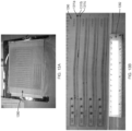
- FIGS. 13A-B illustrate an additional advantage of embodiments of the invention, namely that transducer elements can be printed onto a sheet of PVDF 1390 by depositing a metallic layer, for example.
- FIGS. 13A-B include warped, tapered elements 1311a-c.
- the elements 1311a-c are similar to the warped elements 106a-c illustrated in FIG. 1C , except that the curve functions representing the top and bottom edges on opposing sides of the radiative surfaces of the elements 1311a-c are shallower and broader than functions corresponding to the warped elements 106a-c of FIG. 1C .
- a ruler 1392 is shown in the photograph of FIG. 13B for size perspective.
- the three warped and tapered elements 1311a-c are plated onto the sheet 1390 of PVDF on only one side of the sheet, and only in the regions intended to constitute active elements 1311a-c.
- multiple transducer elements can be plated onto a single sheet of PVDF, providing efficiency and ease of manufacture.
- Other characteristics and advantages of PVDF are described hereinabove in the description of FIG. 10C .
- One advantage of PVDF elements is that they can form part of PVDF layers that can be easily stacked for embodiment transducers including stacked elements. Stacked elements can include rectangular elements, as shown in FIGS. 10B-C , warped elements, as shown in FIGS.
- PVDF enables transducer elements to be manufactured more easily and efficiently. While all or most of the transducer and elements described herein above can be ceramic elements, such as piezoelectric transducers (PZTs), or capacitive transducer elements, many of the element shapes described herein above are complex and can be most easily manufactured by printing corresponding transducer patterns on sheets of PVDF, such as that shown in FIGS. 13A and 13B .
- PZTs piezoelectric transducers
- capacitive transducer elements many of the element shapes described herein above are complex and can be most easily manufactured by printing corresponding transducer patterns on sheets of PVDF, such as that shown in FIGS. 13A and 13B .
- electrostrictive transducer elements can be used in place of PVDF.
- the warped elements of FIGS. 1 , 7A , 7C , 8A , 5A , 12B , 12C , and 12E can be more easily fabricated from PVDF sheets than from ceramic, capacitive, or electrostrictive materials.
- transducer elements with tapered ends such as those illustrated in FIGS. 4A and 8A , for example, and transducer elements with periodic elongations, such as those of FIGS. 11A , 12C, and 12D , for example, can be fabricated more easily from PVDF with metallic deposits thereon.
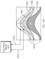
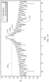
- FIG. 13D is a graph illustrating measured beam patterns in the width (x) dimension.
- the measurements are from a prototype device built using the PVDF elements shown in FIGS. 13A and 13B .
- measured curves 1317a-c are measured radiation patterns for the transducer elements 1311a-c, respectively.
- the corresponding modeled beam pattern for this type of element is illustrated by the curve 852 in FIG 9 .
- curve 852 is the predicted beam pattern in the width dimension.
- the measured beam patterns 1317a-c are similar the predicted curve 852 but slightly narrower than the model. This is not unexpected because the modeled pattern illustrated at 852 in FIG. 9 does not account for the effects of housing diffraction or the backing of the PVDF.
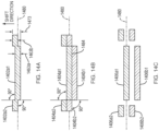
- one or more similar elements with similar shape can be placed adjacent to each other in the same geometric orientation. In yet other embodiments, there are angles other than 90° in the top and bottom edges of element 1402a.
- FIG. 14C illustrates two elements 1406a and 1406b that can form part of an acoustic transducer device.
- the first transducer element 1406a is divided into first and second spatially separated element portions 1406a1-2, which are electrically coupled to each other in a matter described hereinabove in conjunction with FIGS. 12A and 12E , for example.
- the second transducer element 1406b is also divided into first and second spatially separated element portions 1406b 1-2 electrically coupled to each other.
- the second element portions 1406a2 and 1406b2 of the first and second transducer elements are spatially offset from the first element portions of the first and second transducer elements, respectively, in a direction perpendicular to a major axis 1480 of the respective first transducer element.
- FIG. 17B illustrates two skewed diamond-shaped transducer elements 1750 placed in close proximity with each other.
- This configuration illustrates a significant advantage of skewed diamond-shaped transducer elements.
- these elements are advantageous for interferometric transducers because they can be placed with their acoustic centers closer together than for the non-skewed diamond shapes.
- the advantages of having acoustic centers relatively closer together for interferometric designs have been described hereinabove.
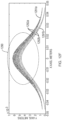
- FIG. 17E is a graph illustrating a Y-direction polar acoustic radiation pattern calculated for both the rectangle transducer shape 1768 and the skewed diamond transducer shape 1770 illustrated in FIG. 17D .
- a Y radiation distribution 1774 is illustrated for the rectangle case, compared with a Y radiation distribution 1776 calculated for the skewed diamond shape 1770 in FIG. 17D .
- side lobes for the skewed diamond distribution 1776 are generally lower than for the rectangular case.
- the strength of the first side lobe 1780 for the skewed diamond case is at a level 1782 of about -16 dB.
- the strength of this first side lobe for skewed diamond cases varies depending on the degree of skew. In particular, as the lengths of the sides ( see, e.g. , FIG. 17A ) become closer to equal, the strength of the first side lobe advantageously decreases, but the minimum spacing along the short axis illustrated in FIG. 17B increases.
Landscapes
- Engineering & Computer Science (AREA)
- Radar, Positioning & Navigation (AREA)
- Remote Sensing (AREA)
- Physics & Mathematics (AREA)
- Acoustics & Sound (AREA)
- Computer Networks & Wireless Communication (AREA)
- General Physics & Mathematics (AREA)
- Mechanical Engineering (AREA)
- Multimedia (AREA)
- Measurement Of Velocity Or Position Using Acoustic Or Ultrasonic Waves (AREA)
- Transducers For Ultrasonic Waves (AREA)
Description
- Side-scan sonar systems are typically configured to detect acoustic radiation within a fan-shaped region that is narrow in a plane parallel to motion of a water vessel and broad in a plane perpendicular to the motion of the vessel. Interferometric sonar measurements using multiple transducer detector elements can be used to determine a direction of an object detected in the water with respect to the water vessel with greater specificity. Phase differences between signals received at multiple acoustic transducers can be used to determine the arrival angle for an acoustic signal detected by the transducers.
- However, aliasing can occur when the phase difference between signals received at the multiple transducers exceeds 360° (phase wrapping), corresponding to one complete temporal or spatial cycle of the received acoustic radiation. Aliasing limits the range of arrival angles that can be reliably determined with a given set of transducer elements.
-
WO 2012/038770 A1 discloses an imaging transducer including a plurality of transducer elements arranged with respect to each other in an array along a long axis of the transducer, wherein an effective width of a transducer element of the transducer is equal to or greater than a center-to-center distance between adjacent transducer elements. -
US 5 889 355 A discloses acousto-optic devices having a sectioned optical transducer with a side passing optical beam forming an acousto-optic interaction plane, an electrode pattern on the transducer, and oblique demarcation cuts in the electrode pattern which are not normal to the acoustic-optic interaction plane. - John E. Meyer et al: "Distributed and discrete transducer spatial design for finite-element-modeled flexible structures" (1994) discloses a modeling technique for transducer spatial design applicable to discrete and distributed transducers with arbitrary one-dimensional shading (spatial gain weighting).
- The invention relates to an acoustic transducer as defined in
claim 1 Further aspects of the invention are set forth in the dependent claims. - There is a need for increasing directionality of acoustic transducer elements for sonar systems in order to minimize or prevent aliasing due to phase wrapping in interferometric transducer systems. These systems include side scan sonar, side looking sonar, synthetic aperture sonar, swath sonar, and all systems that can use interferometry. The present disclosure relates to transducer element configurations that can increase directionality of acoustic transducers in interferometric sonars. Advantageous beam radiation patterns may be obtained. In some embodiments, transducer elements may be constructed of polyvinylidene difluoride (PVDF). PVDF can facilitate construction of a variety of transducer configurations that can be used to narrow transducer receiver beam patterns, while allowing the proper interferometric spacing between receivers. Embodiments can enable simultaneous control of element beamwidth to minimize spatial aliasing, radiation side lobe level to reduce echo contamination, and channel-to-channel spacing in an acoustic interferometer.
- The foregoing will be apparent from the following more particular description of example embodiments of the invention, as illustrated in the accompanying drawings in which like reference characters refer to the same parts throughout the different views. The drawings are not necessarily to scale, emphasis instead being placed upon illustrating embodiments of the present invention.
-
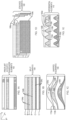
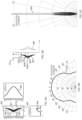
FIG. 1A illustrates prior art acoustic transducer elements. -
FIGS. 1B-1E illustrate transducer elements, whereinFIG. 1C is according to the invention. -
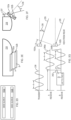
FIG. 2A is a perspective illustration of typical side-scan sonar geometry. -
FIGS. 2B-2C includes side-view and top-view illustrations of angles relevant to side-scan sonar imaging. -
FIG. 2D illustrates a typical two-element transducer used in interferometric side-scan sonar imaging. -
FIGS. 2E-F illustrate how the transducer ofFIG. 2D can be mounted to a water vessel. -
FIG. 2G illustrates transmit and receive signals and angles relevant to interferometric side-scan sonar imaging using the two transducer elements illustrated inFIG. 2D . -
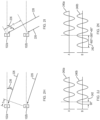
FIGS. 2H-I illustrate differences in geometry for interferometric sonar imaging with shallow and steep angles, respectively. -
FIGS. 2J-K illustrate phase differences in transducer receives signals for the shallow and steep measurement angles illustrated inFIGS. 2H-I , respectively. -
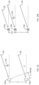
FIGS. 2L-M illustrate geometries relevant to calculation of phase wrapping conditions for two-element and three-element interferometric sonar systems, respectively. -
FIG. 2N is a table with two-element interferometer wrapping angles and corresponding 10 dB and 20 dB rejection angles for rectangular and circular element implementations of the two-element interferometer. -
FIGS. 3A-E illustrate element shape, amplitude distributions, spatial Fourier transform, and X and Y polar radiation distributions for prior art rectangular transducer elements. -
FIGS. 4A-E include graphs similar to those ofFIGS. 3A-E , respectively, for diamond-shaped transducer element not forming part of the present invention. -
FIGS. 5A-E include graphs similar to those ofFIGS. 3A-E , respectively, for a prior art transducer element having tapered ends and edges symmetric to one another. -
FIG. 6A-C illustrate comparisons between element shapes, X axis amplitude distributions, X axis polar radiation patterns, and transducer configurations for a prior art rectangular transducer element and a split element for interleaving elements according to an embodiment of the invention. -
FIG. 7A-C include comparison illustrations similar to those ofFIGS. 6A-C , respectively, for the prior art rectangular element shape compared with an embodiment warped element shape. -
FIG. 8A illustrates element shape and X and Y amplitude distributions for an embodiment tapered, warped transducer element. -
FIGS. 8B-C are graphs illustrating calculated X axis and Y axis polar radiation distributions, respectively. -
FIG. 8D illustrates how embodiment warped elements have an overall width greater than any local width and can lack inversion symmetry. -
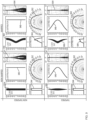
FIG. 9 illustrates the effects of warping and tapering transducer element shapes upon the amplitude distributions and radiation patterns. -
FIG. 10A illustrates a spacing between acoustics centers for the prior art transducer elements illustrated inFIG. 1A . -
FIGS. 10B-C illustrate stacked transducer elements. -
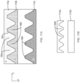
FIG. 11A illustrates transducer elements not forming part of the present invention with periodic elongations configured to interleave with one another. -
FIG. 11B illustrates a transducer element not forming part of the present invention with sinusoidal periodic elongations. -
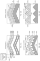
FIG. 12A illustrates embodiment warped and divided transducer elements. -
FIG. 12B illustrates embodiment warped and stacked transducer elements. -
FIG. 12C illustrates warped transducer elements with periodic sawtooth elongations according to an embodiment. -
FIG. 12D illustrates stacked transducer elements not forming part of the present invention with sawtooth periodic elongations. -
FIG. 12E illustrates embodiment warped, tapered, stacked transducer elements with an electrical circuit connected thereto. -
FIG. 12F is a graphical illustration of an embodiment set of transducers with non-contiguous sub-elements interspersed with each other in the same plane. -
FIGS. 13A-B are photographs showing embodiment warped, tapered transducer elements printed onto a sheet of polyvinylidene difluoride (PVDF) for prototyping. -
FIG. 13C is a model illustrating how transducers such as those illustrated inFIGS. 13A-B can be configured for side-scan applications with through-hull mounting. -
FIG. 13D is a graph illustrating measured beam patterns in the width (x) dimension for a prototype device constructed using the warped elements shown inFIGS. 13A-B . -
FIGS. 14A-B illustrate warped transducer elements not forming part of the present invention with edges defining 90° angles. -
FIG. 14C illustrates a transducer element not forming part of the present invention with element portions spatially separated and offset from one another. -
FIG. 15 illustrates a warped sawtooth transducer element not forming part of the present invention. -
FIG. 16 illustrates a warped sinusoidal transducer element not forming part of the present invention. -
FIGS. 17A-C illustrate various acoustic transducers having one or more transducer elements with acoustic radiative surfaces with skewed diamond shapes and which do not form part of the present invention. -
FIG. 17D is a graph illustrating computational points used to model rectangular and skewed diamond transducer shapes to determine the side lobe structure, not forming part of the present invention. -
FIGS. 17E is a graph illustrating the relative Y axis radiation amplitude distributions for the rectangular and skewed diamond-shaped elements as represented inFIG. 17D , not forming part of the present invention. -
FIG. 17F is a detailed view of the graph inFIG. 17E not forming part of the present invention, showing only the angular range -20° - +20°. - A description of example embodiments of the invention follows.
-
FIG. 1A illustrates a prior artacoustic transducer 102 that includes threetransducer elements 102a-c that can be used for interferometric side-scan sonar measurements, for example. In particular, theelements 102a-c are rectangular, which is a typical geometry used for side-scan imaging systems for ease of manufacture and to produce the appropriate radiation pattern for side-scan imaging, as illustrated further inFIG. 2A . -
FIGS. 1B-1E illustratevarious transducers FIG. 1A while maintaining both receiver sensitivity and acoustic center-to-center element spacing (illustrated inFIG. 10 ). In particular, thetransducer 104 includes split (divided)elements FIG. 12A . With the electrical coupling between theelement portions 104a, for example, theelement portions 104a can be driven by the same electrical signal, with the same driving frequency and wavelength to produce radiation as a single transducer element but with a radiation distribution that is narrower than if theelement portions 104a were spatially coupled to each other.FIG. 1B illustrates that a transducer withelement 104a can include one or more additional elements (e.g. elements 104b-c), each additional element divided into at least two spatially separated element portions. The spatially separated element portions of each additional element can be electrically coupled to each other to be driven or to receive as a single element, as described further hereinafter. - With the
element portions 104b spatially separated from each other but electrically coupled to each other, theelement portions 104b also act as a single transducer and can be configured to interleave with theelements 104a as shown inFIG. 1B . In particular, oneelement portion 104a is situated between the twoelement portions 104b. The dividedelements 104a-c are further described hereinafter in conjunction withFIGS. 6A-C andFIG. 10A . Moreover, as illustrated inFIG. 12A , divided elements need not be rectangular and can have other shapes in other embodiments. Furthermore, while three sets of dividedelements 104a-c are illustrated inFIG. 1B , in other embodiments, only two sets of split elements are present in a transducer. -
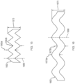
FIG. 1C illustrates atransducer 106 withwarped elements 106a-c. Thewarped elements 106a-c have acousticradiative surfaces 182a-c, respectively. Each radiative surface includes twowarped edges respective radiative surfaces 182a-c. Furthermore, while additional transducer elements (firstwarped element 106a and additionalwarped elements 106b-c) are shown inFIG. 1C , in other embodiments, only onewarped element 106a is required (e.g., where interferometric measurements are not required). Warped elements are further illustrated and described in conjunction withFIGS. 7B-C ,8A-D ,9 ,12A-C ,12E , and13 , for example. - The
warped elements 106a-c have smooth edges, meaning that there are no angles formed in the edges. In other embodiments, as described hereinafter in connection withFIG. 12C and14A , for example, angles may be formed in the edges, such as 90° angles or angles forming a sawtooth pattern in the edges, for example. -
FIG. 1D illustrates atransducer 108 with stackedplanes 108a-c containing elements. Each plane can contain an element shaped such as warped Gaussian (e.g. 182a), or a rectangle (e.g. 102a), or sawtooth (e.g. 182a inFIG. 1E ). There are two views inFIG. 1D : a perspective, exploded view (left), and a side-view (non-exploded) (right). While threestacked element planes 108a-c are illustrated inFIG. 1D , in other embodiments, only two stacked element planes are used. Stacking elements enables elements to be wider along the X axis, which narrows the radiation distribution in the XZ plane for more directive radiation patterns while maintaining a center-to-center spacing of acoustic centers of theelements 108a-c, as further illustrated inFIG. 10B . Stacking works when each transducer element is acoustically transparent, allowing wave penetration to reach each of the stacked planes without substantial loss of energy. This is particularly useful with PVDF transducers. Theembodiment transducer 108 is further illustrated inFIGS. 10B-C . Some examples of non-rectangular, stacked elements are illustrated inFIGS. 12B and12D-E , for example. -
FIG. 1E illustrates atransducer 110 withinterdigital elements 110a-c. Thetransducer elements element 110b. Each of theelements 1 10a-c has an acousticradiative surface 182a-c, respectively, with an edge havingperiodic elongations 186a-c, respectively, protruding therefrom. Each of thetransducer elements 1 10a-c, therefore, includes an acousticradiative surface 182a-c with an edge having periodic elongations with a partial sawtooth shaped. - In other examples, the transducer can vary from the
transducer 110 illustrated inFIG. 1E and can include only two transducer elements, for example. Furthermore, in some examples, only one of the transducer elements has an edge with periodic elongations. In yet other examples, theinterdigital elements 1 10a-b do not fit together to form acommon edge 184, as shown inFIG. 1E . In still other examples, an acoustic transducer includes only thesingle element 110a, an edge of the radiative surface having periodic elongations protruding therefrom, the edge defining a periodic shape. The configuration of thetransducer elements 1 10a-c also allows for the radiation distribution in the XZ plane to be narrowed compared to a radiation pattern produced by theelements 102a-c, for example, while enabling the same spacing between acoustic centers (not shown). Theinterdigital elements 1 10a-c are also illustrated inFIG. 11A , and other example devices including transducer elements with periodic elongation are illustrated inFIGS. 12C-D . - It should be noted that there is an equivalency between the radiation pattern produced when a transducer is driven to produce acoustic radiation and the pattern indicating the sensitivity of a transducer to radiation received by the transducer when it is operated in detection mode. Therefore, throughout this application, when radiation patterns are described, it should be understood that radiation detection patterns are equivalent to radiation production patterns in terms of strength distribution. Furthermore, while both prior art transducers, such as the
transducer 102 inFIG. 1A as well astransducers FIGS. 1B-1E , can be used to both transmit acoustic radiation and to detect acoustic radiation at different times, in some cases, separate transducers can be used for transmitting acoustic radiation, and the use of embodiment transducers can be confined to detection. All the radiation patterns and embodiments described herein are relevant to detection receiver applications. -
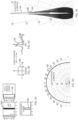
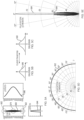
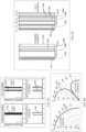
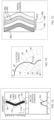
FIG. 2A is a perspective illustration of a typical side-scan sonar imaging application. Atowfish 212, which can be pulled behind a boat or other water vessel, has the prior artacoustic transducer 102a mounted thereon. Thetransducer 102a both produces acoustic radiation and detects reflected radiation over a fan-shapedregion 214. Thetowfish 212 also includes a second prior art transducer (not shown) on the other side of the towfish that produces asecond radiation pattern 214 on the other side of the towfish. These are usually referred to as the port and starboard transducers. Objects anywhere in thedetection regions 214 or at aseabed 216 can be detected.Transducer 102 is traditionally long in the Y direction and narrow in the X direction, so that its radiation patterns (for both transmit and receive) are narrow along Y and wide in the XZ plane. Thetowfish 212 travels in the Y direction indicated inFIG. 2A , with an X direction perpendicular to the direction of travel and a Z direction perpendicular to both X and Y axes. As described further hereinafter, interferometric transducers can be used to narrow a region within which a detected object can be determined to be situated. WhileFIG. 2A shows atowfish 212 with theacoustic transducer 102a, theacoustic transducer 102a can also be mounted to a boat (illustrated inFIG. 2B ) or any other water vessel, for example. -
FIGS. 2B-2C illustrate angles relevant to side-scan sonar imaging. In particular, aboat 218 having afront section 220, arear section 222, and atop section 224 travels in the Y direction on the water. A dashedline 226 joins a transducer (not shown) on theboat 218 and a detection object 228 (a fish inFIG. 2B ). A dashedline 230 extends from theboat 218 in the direction of thedetection object 228 but in the X-Y plane.FIG. 2B includes a side view of theboat 218 traveling in a Y direction on water in the X-Y plane. For side-scan imaging, anazimuth angle 232 between the Y-axis and theline 230 is well known due to the shape of the radiation pattern illustrated inFIG. 2A . However, theangle θ 236, which is equal to 90° minus theangle 234 from a nadir (-Z axis), is not well known unless interferometric sonar measurements are used.FIG. 2C is a top view of theboat 218 andobject 228. -
FIG. 2D illustrates a typical acoustic transducer configuration including the tworectangular elements FIG. 2B ) with greater accuracy. -
FIGS. 2E-F are side-view and rearview illustrations showing where thetransducer elements -
FIG. 2G illustrates typical signals and geometry using a dual transducer configuration such as the configuration illustrated inFIGS. 2D-F . The left side ofFIG. 2G illustrates atransmission signal 238, which can be produced by thetransducers 102a-b or by a separate transducer (not shown). Thetransmission signal 238 and receivedsignals transducers difference 242 and target distance measured by thereceivers arrival angle θ 236, as understood in the art of interferometric transducers. Namely, a time-of-arrival difference between the signal received at thetransducer 102a and the signal received at thetransducer 102b can be used to determine a path length difference Δ which in turn can be used to determine the arrival angle θ. The target angle from the nadir is thearrival angle θ 236 plus a mountingangle ϕ 237 illustrated inFIG. 2F . -
FIGS. 2H-K illustrate a phase wrapping issue that can occur in interferometric sonar measurements when the arrival angle θ is too large.FIG. 2H is the same diagram shown on the right side ofFIG. 2G , in which thearrival angle θ 236 is relatively small. When θ is small, the path difference Δ forradiation 226 arriving at thetransducers FIG. 2I shows corresponding values when the arrival angle θ is relatively large. In this case, the path difference forradiation 226 arriving at the twodetectors -
FIGS. 2J and 2K illustrate further effects of small and large arrival angles, respectively, on interferometric measurements. Here, it should be noted that in practice, aphase difference 242 between signals received at the transducers, rather than a time difference, is used to determine the angle θ.FIG. 2J illustrates thephase difference 242 for the case of the relatively small arrival angle inFIG. 2H . In this case, thephase difference 242 between thesignals transducers difference 90° is smaller than a full cycle of 360°, the arrival angle θ can be determined unambiguously. In contrast, inFIG. 2K , corresponding to the large arrival angle θ inFIG. 2I , thephase difference 242 for the arriving signals is 450° = 360° + 90°. Thus, the phase-based measurement inFIG. 2K yields the same results as the phase-based measurement inFIG. 2J when calculations to determine the angle θ are performed, and the angle θ can be erroneously calculated to be the same for bothFIGS. 2H and 2I . In other words, reflections arriving from steep arrival angles can be processed as arriving from shallow arrival angles. It is desirable, therefore, to have transducer receivers with narrower beams in the XZ plane than the large fan-shapedbeams 214 illustrated inFIG. 2A . A phase difference of 360° is the limit at which phase can be determined unambiguously, and an arrival angle θ corresponding to the phase difference of 360° is called the wrapping angle. When thephase difference 242 exceeds 360°, as shown inFIG. 2K , this is referred to as phase wrapping. - The desirability for relatively narrower beams in the XZ plane and for close spacing of transducers can also be explained in further reference to
FIG. 1A and 1B , as follows. InFIG. 1A , the three channels (from threeacoustic elements 102a-c) are at different vertical axis positions, as illustrated in the figure. Note that each transducer (channel) 102a, 102b, or 102c also has a small finite vertical width. The width for each element could be made smaller, making the vertical beam for each element wider. Conversely, the respective vertical widths could be made larger, thereby making the respective vertical beams for each element narrower. This is a consequence of the inverse relationship between wavelength λ and aperture length L, and the resulting radian beamwidth λ/L. - It is usually preferable for a mapping sonar system to have its transmit, receive, or both apertures designed to ignore echoes from zenith or from nadir, with respect to the sonar's main radiation lobe direction, because these extraneous echoes corrupt the desirable echoes from the intended mapping region in the forward- or side-looking direction. This means that the vertical aperture of a single acoustic channel should have a height extent (to control its own vertical beamwidth), and shape (to control its own vertical side lobes) to reduce energy from directly overhead (zenith) surface scattering or from the directly beneath from bottom scattering, or multiple bounces from both. In a single channel system, without interferometry, this imposes no restrictions other than transducer space. However, in an interferometric system with more than one transducer, the desired single-channel vertical beam width and side lobe control, can conflict with the center-to-center vertical separation of the interferometer channels. Embodiments described herein have the advantage of providing favorable characteristics simultaneously for side lobe control, center-to-center interferometer separation, and main beam width.
-
FIG. 1B illustrates how the desired vertical separation between interferometer channels can be maintained, while at the same time having some control over each channel's vertical beamwidth. InFIG. 1B , the effective vertical center ofchannels FIG. 1A , even though each element is geometrically divided into two pieces that are electrically coupled. -
FIGS. 2L and 2M are used to illustrate far-field phase wrapping conditions for two-element and three-element transducer arrays. InFIG. 2L , which illustrates the two-element case, the twotransducer elements FIG. 2G ) of theacoustic radiation 226 received. This relationship can be expressed as
-
FIG. 2M illustrates a common three-element configuration (also illustrated inFIG. 1A ). In the three-element case, the same phase wrapping conditions described above for the two-element case, namely, that there is phase wrapping for d > λ, apply for each pair of elements used in the array. Varied spacing between pairs of elements allows greater flexibility in measurements. For example, theelements elements elements outer pair FIG. 2M . For example, theelements 102a-102c, with the largest spacing 1.5 λ, have a 42° wrapping angle (for a sonar used in water, with nominal 1500 m/s sound speed). Thus,FIGS. 2L and 2M further illustrate the desirability of having transducer receivers that are more directional in the XZ plane illustrated inFIG. 2A to avoid phase wrapping. -
FIG. 2N includes a table that lists examples of two-element interferometer phase wrapping angles. The 10 dB and 20 dB rejection angles for implementations with standard rectangular and circular elements are also shown. For example, if the center-to-center spacing d between the elements is 1.5 λ, the interferometer phase wrapping angle is 42°. The largest rectangular elements that can be used are 1.5 λ wide (no gap between) which have 10 dB and 20 dB rejection angles of 29° and 37°, respectively, in water. Similarly, the largest circular elements that can be used are 1.5 λ in diameter, which have 10 dB and 20 dB rejection angles of 35° and 47°, respectively, in water. - The above examples illustrate that for two-element interferometers, if 10 dB rejection is sufficient, standard transducer elements such as
elements 102a-c inFIG. 1A , will be sufficient. However, if 20 dB rejection is required, for example, disk-shaped elements will not be sufficient, and rectangular-shaped elements barely meet the 20 dB rejection requirement under the best-case scenario of having no gap between the elements. In addition, the rejection angles listed in the table inFIG. 2N are for the main lobe of radiation. Rectangular elements have a peak side lobe amplitude of approximately -13 dB and thus would fail the 20 dB rejection requirements in many circumstances. Furthermore, these considerations are based on calculations using the widest possible elements. In practice, however, neither standard disk-shaped elements nor standard rectangular elements are likely to work when 20 dB rejection is required. - For the three-element case illustrated in
FIG. 2M , the phase wrapping angle in water is θ = 42°, assuming that theelements adjacent transducer elements FIG. 2M , neither standard element can provide 10 dB of rejection at any angle, and it should also be noted that both standard elements have very little rejection (1 to 2 dB) at 42°. Thus, if more than 10 dB of rejection is required, both standard rectangular and standard disk elements are unacceptable. - For an arbitrary array of standard elements with largest element spacing d, the phase wrapping angle is

- As described in part in conjunction with
FIGS. 1B-E , these difficulties can be overcome by stacking or dividing transducer elements, for example. However, both these and additional benefits can also be obtained by devices that include warped transducer elements or transducer elements with protrusions, for example. Embodiments can significantly narrow radiation detection patterns in the XZ plane while maintaining small side lobes in radiation detection patterns in the YZ plane, for example. - Reshaping of the aperture (transducer shape) can allow further control of each channel's vertical beamwidth and beam pattern structure (i.e. the main lobe plus all side lobes). The connection of aperture shape, main lobe width, and side lobe locations and strength is known in the context of Fourier transforms. In signal processing, a time domain waveform can be filtered using windowing techniques together with the Fourier transform. In other applications such as radar, acoustics, and optics, a spatial Fourier transform (i.e. a beam pattern) occurs when an aperture sends (or receives) energy from the far field of the aperture. The beam pattern shape may be altered by altering the window shape. Thus, principles used in signal processing can similarly be used in radar, acoustics and optics, because they use similar mathematics.
- To avoid conflict between the channels' center-to-center spacings, while also altering the window shape for each channel to affect each channel's beam pattern in a desirable way, taper shapes such as the Gaussian shape illustrated in
FIG. 1C are used. To prevent each channel from physically interfering with adjacent channels, the shapes can be warped such that each effective channel center vertical position is maintained for the needs of interferometry, while at the same time the shape and warping achieve the desired vertical beam pattern (main lobe width, plus side lobe control). - Embodiment devices are warped, such as shown in
FIG. 1C , which has significant benefits in addition to devices that are not so shaped, even beyond the advantages of devices with rectangular shapes, as shown inFIG. 1B , for example. InFIG. 1B , the vertical aperture has center-to-center spacings to meet interferometer system needs, and it also provides control of the vertical beam pattern shape because it has a taller vertical span, thus allowing a narrower vertical beam. However, for some vertical angles, side lobes in the radiation pattern can increase. Warped configurations such as shown inFIG. 1C also provide a continuous aperture distribution, without spatial breaks, so that the side lobe radiation pattern structure will decrease. The Gaussian shape of the device inFIG. 1C also controls the location and level of side lobes in both vertical and horizontal planes. This is an additional benefit not obtained by either prior art devices, such as illustrated inFIG. 1A , nor example devices having only split elements, as illustrated inFIG. 1B . -
FIGS. 3A-3E and5A-5E include examples of prior art transducer shapes and their corresponding radiation detection distributions for comparison purposes, whileFIGS. 4A-E illustrate an example diamond element shape and corresponding radiation detection distributions for comparison purposes. -
FIG. 3A illustrates the element shape for therectangular element 102a shown inFIG. 1A . As illustrated in the graphs inFIG. 3A , therectangular element shape 102a gives rise to a radiationdetection amplitude distribution 344 in the X dimension, with another rectangular radiationdetection amplitude distribution 346 in the Y dimension. Theserectangular amplitude distributions FIG. 3B . -
FIGS. 3B and 3C illustrate the relationship between the boxcar or rectangular amplitude distribution of a receiver or source and the far field polar radiation distribution. Namely, the amplitude distribution and far field radiation pattern are related by Fourier transform, as understood in the art of sonar transducer construction. The rectangular "boxcar"distribution 348 shown inFIG. 3B yields a far-field sincradiation pattern 350, illustrated inFIG. 3C , when a spatial Fourier transform is performed. It should be noted that the amplitude distribution in 348 is shown as a function of time, and the Fourier transform leads to thetemporal frequency distribution 350 shown inFIG. 3C . However, the relationship between a spatial amplitude distribution (such as the Y distribution 346) and the spatial frequency distribution, is the same, so the term spatial Fourier transform is used. -
FIGS. 3D-E are graphs illustrating the X dimension and Y dimension polar radiation distributions, respectively, calculated by spatial Fourier transform and ray tracing for theelement shape 102a. In particular,FIG. 3D is a polar graph illustrating a Y dimensionpolar radiation distribution 352 in the XZ plane illustrated inFIG. 1A , with 0° being centered on an axis normal to the transducer surface. The contours in the plot are in dB units. As can be seen inFIG. 3A and FIG. 3D , a relatively narrower X dimension amplitude distribution corresponds to a relativelywide radiation distribution 352. -
FIG. 3E is a polar graph illustrating a Y dimensionpolar radiation distribution 354 in a plane intersecting the Y-axis illustrated inFIG. 2A . Thehighest side lobe 356 in theradiation pattern 354 reaches a level of -13 dB. -
FIGS. 4A-E are similar to theFIGS. 3A-3E , except that theFIGS. 4A-E correspond to an existing diamond-shapedelement 460 illustrated inFIG. 4A . TheX amplitude distribution 444 andY amplitude distribution 446 are triangular, andFIGS. 4B-C illustrate that atriangular amplitude distribution 448 corresponds to a sinc2 frequency distribution 450.FIG. 4D shows the X dimension polarradiation distribution pattern 452 corresponding to the Xdimension amplitude distribution 444 shown inFIG. 4A. FIG. 4E illustrates a Y dimension polarradiation distribution pattern 454 corresponding to theamplitude distribution 446 shown inFIG. 4A . Thehighest side lobe 456 for theY distribution 454 reaches a level of -27 dB. While the side lobes ofFIG. 4D (including the highest side lobe 456) are smaller than those ofFIG. 3B for the Y dimension, theX dimension pattern 452 is wider than the corresponding pattern inFIG. 3D for the rectangular shape. Thus,FIGS. 4A and 4D illustrate that an arbitrary modification of theelement shape 102 inFIG. 3A will not lead to helpful results as to narrowing the X dimension radiation pattern to make it more directive as desired. -
FIGS. 5A-E are similar toFIGS. 3A-E and4A-E , except thatFIGS. 5A-E correspond to atapered element 560 illustrated inFIG. 5A . The general shape of theelement 560 has been used to decrease side lobes in the Y dimension, as illustrated inFIG. 5E , as well as narrow the radiation distribution in the X dimension, as illustrated inFIG. 5D . Theelement 560, like theelement 460 inFIG. 4A , has tapered ends 562. The tapered ends 562 are smaller in local width than acenter section 574 of the element. While theends 562 come to a point, in other examples, tapered ends do not come to a point. Thus, as used herein, "tapered" or "tapered ends" refers to ends of a transducer element having a smaller width than a center section of the transducer element. Theelement 560 has anX amplitude distribution 544 and aY amplitude distribution 546. TheY amplitude distribution 546 has a largely Gaussian shape. As illustrated inFIGS. 5B-C , the Fourier transform of theGaussian function 548 is alsoGaussian function 550. -
FIG. 5D shows an X dimension polarradiation pattern distribution 552 corresponding to theamplitude distribution 544 shown inFIG. 5A. FIG. 5E shows a Y dimension polarradiation distribution pattern 554 corresponding to theamplitude distribution 546 shown inFIG. 5A . It should be noted that, as shown inFIGS. 5B and 5C , a full Gaussian amplitude distribution corresponds to a full Gaussian radiation pattern with no side lobes. However, for any real implementation of an element, a Y amplitude distribution will be truncated, as shown in theY distribution 546 inFIG. 5A . Thus, in real implementations, there will be side lobes in a Y radiation distribution, as shown inFIG. 5E , but the side lobes can be made very small, such as thehighest side lobe 556 around -30 dB. -
FIGS. 6A-C are used to show how the divided (split)elements 104a-c can be used to narrow X dimension polar radiation distribution patterns.FIGS. 6A-C also include shapes and graphs corresponding to the standardrectangular element shape 102a fromFIG. 1A . Theelement 104a is divided into two spatially separated element portions that are electrically coupled to each other. This is in contrast to thestandard element shape 102a, which is one, undivided structure. The electrical coupling between theelement portions 104a can be done via an electrical circuit, for example, as illustrated inFIG. 12A , for example, which drives both element portions together or receives detected signals from theelement portions 104a, treating them as a single element.Element portions 104a andFIG. 6A are equal in size, but in other embodiments, theelement portions 104a are not equal in width.FIG. 6A also shows Xdimension amplitude distributions standard element 102a and dividedelement 104a, respectively. Therectangular element portions 104a are rectangular in shape and have longer sides oriented parallel to one another and also parallel to an axis along which theelement 104a is divided, namely an axis parallel to the y axis and centered at zero along the x axis inFIG. 6A . -
FIG. 6B illustrates X dimension polarradiation distribution patterns 352 and 652, corresponding to theamplitude distributions FIG. 6B , one advantage of the divided element design is that it achieves some narrowing in the X dimension radiation pattern 652 compared with thepattern 352 for thestandard element 102a. This corresponds to the wider overall Xdimension amplitude distribution 644 achieved by dividing theelement 104a into two portions. While theelement 104a is divided into two portions, and other embodiments, the element is divided into three or more portions. The narrowing of the spectrum and 652 shown inFIG. 6B is particularly significant in the range between 40° and 60°. -
FIG. 6C illustrates how three divided elements can be incorporated into a three-element transducer. Namely, in addition to theelement portions 104a, other dividedelements 104b and 104c are also used.FIG. 6C illustratesacoustic centers 668a-c corresponding to each of thestandard elements 102a-c and each of the dividedelements 104a-c. Theacoustic center 668a, for example, is located between the dividedelement portions 104a, with the otheracoustic centers 668b-c located between respective pairs ofelement portions 104b and 104c, respectively. - One advantage of the embodiment split
elements 104a-c illustrated inFIG. 6A and 6C is that separations between acoustics centers of the elements can be maintained, relative to thestandard elements 102a-c, even while the X amplitude distribution is broadened relative to the standard element case. Thus, theseparation 667a between theacoustic centers FIG. 6C . Similarly, theseparation 667b between theacoustic centers FIG. 6C . In some embodiments, such as the split-element design shown inFIG. 6C , at least one element portion of one transducer element is in physical contact with at least one element portion of another divided transducer element. InFIG. 6C , this is the case for one element portion oftransducer element 104a and one portion oftransducer element 104b. -
FIGS. 7A-C are similar to the right sides ofFIGS. 6A-C , respectively. However,FIGS. 7A-C include illustrations corresponding to an embodimentwarped element 768a shown inFIGS. 7A and 7C. FIGS. 7A-C can be compared and contrasted with the left sides ofFIGS. 6A-C (corresponding to the standardrectangular element shape 102a fromFIG. 1A ), respectively. - As used herein, "warped" denotes an element shape that has an overall width greater than any local width of the element, as further illustrated in
FIG. 8D . Warped elements can further lack inversion symmetry with respect to the Y axis, as illustrated inFIG. 8D . It should be understood that warping and tapering are two different characteristics. Tapered elements, as described hereinabove in conjunction withFIG. 4A , include elements with ends that are narrower (smaller in width) than a center portion of the element, while warped elements include those with an overall width greater than any local width of the element, as illustrated further inFIG. 8D . A warped element, such as thewarped element 768a, contrasts with elements that are only tapered but not warped, such as thetapered element 560 inFIG. 5A , for example. It will be noted that theelement 560 inFIG. 5A has inversion symmetry and has an overall width that is the same as the maximum local width. Theelement 768a includes twowarped edges sides element 768a. Each of the warped edges has the same shape, with the shape having the same function parameters. Theelement 768a is not tapered; namely, ends 762 have widths equal to the width of thecenter portion 774. However, in other embodiments, such as the embodiment shown inFIG. 8A , warped elements are also tapered. Further, in some embodiments, such as 106a-c, each tapered end comes to a point, joining the two warped edges at each tapered end. Furthermore, in other embodiments, theedges edges - An X dimension
radiation amplitude distribution 744 for theelement 768a is broader than the corresponding Xdimension amplitude distribution 344 for therectangular element 102a. Thebroader amplitude distribution 744 leads to a corresponding narrower X dimensionpolar radiation pattern 752 inFIG. 7B. FIG. 7C illustrates how thewarped element 768a can be used with similarwarped elements 768b-c for use in a three-element transducer. Because theelements 768a-c are warped, the corresponding dashedlines 769a-c do not represent acoustic centers of the elements, as the dashedlines 668a-c do for thestandard elements 102a-c. Acoustic centers (not shown) for theelements 768a-c would be shifted to the right of the dashedlines 768a-c, respectively. However, theseparations adjacent element 768a-b and 768b-c, respectively, do represent the relative separation between acoustic centers of the adjacent warped elements. Thus, the acoustic centers (not shown) for thewarped elements 768a-c can have the same spacing as the standardrectangular elements 102a-c. -
FIGS. 8A-D pertain to anembodiment transducer element 860, shown inFIG. 8A . Theelement 860 is tapered, because it has ends 862 smaller in width than acenter portion 874 of the element. Twoedges 872a and 872b of the elements both have substantially similar shapes, but the shape of theedge 872a follows a shallower curve than the edge 872b. Theedges 872a-b are edges of aradiative surface 864 of theelement 860. Theelement 860 has a substantially GaussianY amplitude distribution 846 and anX distribution 844. X and Y dimensionpolar radiation distributions FIGS. 8B and 8C , respectively. The GaussianY amplitude distribution 846 is truncated, as further described hereinabove in relation toFIG. 5A . -
FIG. 8D illustrates that warped elements are defined, as used herein, as having an overall width of a radiative surface of the element being greater than any local width of the radiating surface of the element. InFIG. 8D , anoverall width 873 is greater than any of thelocal widths 863a-c. Other example transducer elements that are warped and share this characteristic of overall width include theelements 768a-c (seeFIG. 7A and 7C ) andelements 1202a-c, 1203a-c, and 1205a-c (described hereinafter in conjunction withFIGS. 12A, 12B, and 12C , respectively). - Warped edges of a transducer element are edges on opposing sides of a radiative surface of a transducer element that define shapes that result in the transducer element being warped. For example, the
warped edges 872a and 872b (illustrated inFIG. 8A ) are edges on opposing sides of theelement 860 that define shapes causing theelement 860 to be warped (having an overall width of the radiative surface of the element that is greater than any local width of the radiative surface of the element). Some warped edges define shapes that are not smooth. Furthermore, some warped edges define shapes that are periodic, with warped sawtooth or other warped periodic edges with periodic elongations, for example. One example is described hereinafter in conjunction withFIG. 12C . InFIG. 12C , asawtooth edge 1284 and smooth edge 1213a are warped edges and define awarped element 1205a having periodic elongations from thesawtooth edge 1284. -
FIG. 8D also illustrates that warped elements can lack of inversion symmetry. For example, theelement 860 is shown on the left, while a mirror image 860' of the element is shown on the right side of the Y axis illustrated inFIG. 8D . It should be noted that some elements, such as elements 110 (seeFIG. 1E ) and 1110a (described hereinafter in conjunction withFIG. 11B ), similarly lack inversion symmetry. However,elements 110 and 11 10a are not warped because they do not have an overall width of a radiative surface greater than any local width of the same radiative surface of the same element. -
FIG. 9 illustrates effects of tapering and warping elements on X and Y amplitude distributions and X and Y polar radiation distributions. In particular,non-warped elements FIG. 9 , whilewarped elements FIG. 9 . Theelements FIG. 9 are not tapered, while theelements FIG. 9 are tapered. - The upper left of
FIG. 9 illustrates therectangular element shape 102a, X andY amplitude distributions polar radiation distributions FIGS. 3A, 3D, and 3E . In contrast to therectangular element 102a, theelement 902 in the upper right ofFIG. 9 is warped. While aY amplitude distribution 946 and Ypolar radiation pattern 954 are not substantially different from those of thestandard element 102a, anX amplitude distributional 944 is substantially broader than theX distribution 344 for therectangular element 102a, and an X polar radiation distribution 952 is substantially narrower than thedistribution 352 corresponding to the rectangular element. - The
tapered element 560 at the bottom left ofFIG. 9 has a broaderY amplitude distribution 546 and narrower Y axispolar radiation distribution 554 compared to theY distribution 346 andY radiation distribution 354 for the standard element shape. However, anX amplitude distribution 544 corresponding to the taperedelement 560 is overall narrower than theX amplitude distribution 344 for thestandard element 102a. Furthermore, an Xpolar radiation distribution 552 corresponding to the taperedelement 560 is broader than theX radiation distribution 352 for the standard element. This illustrates that tapering alone may not necessarily narrow X radiation patterns, as desired for increased directionality in acoustic receivers, as described hereinabove. Theelement shape 860 at the lower right ofFIG. 9 and is the same element illustrated inFIG. 8A . Notably, the Xpolar radiation distribution 852 is even narrower than the corresponding distribution 952 for theelement 902 that is only warped. Furthermore, the Ypolar distribution 854 has significantly smaller side lobes than the corresponding Ypolar radiation distribution 954 for theelement 902 that is only warped. In particular, the X polar radiation distribution is attenuated to a level of about -20 dB for arrival angles steeper than about +/-60°. Thus, warping elements can provide significant advantages in directivity of sonar transducer elements, and tapering in addition to warping can provide yet further advantages in narrowing the distributions. -
FIGS. 10A-C illustrate how transducer elements can be stacked to increase sensitivity and decrease X axis polar radiation distributions.FIG. 10A illustrates therectangular elements 102a-c for comparison withstacked elements 108a-c illustrated inFIG. 10B . While rectangular stacked elements are illustrated inFIGS. 10B-C , the stacking principles illustrated can apply to many embodiments described herein that use non-rectangular element shapes. For example,FIG. 12E illustrates warped elements that have the additional advantages of stacking, as described hereinafter. Thecoordinates 1021a apply to the stacked elements on the left ofFIG. 10B . The right side ofFIG. 10B , to which coordinates 1021b apply, show and end-on view of thestacked elements 108a-c.FIG. 10C , to which coordinates 1021c apply, is a rotated and on view of thestacked elements 108a-c. - The
elements 108a-c are much wider than thestandard elements 102a-c ofFIG. 10A . As understood by those skilled in the art of acoustic transducer design, widening the transducer elements in the X direction significantly narrows the corresponding radiation pattern in the XZ plane. Furthermore, widening the transducer elements can also increase transducer sensitivity and increase signal-to-noise ratios. However, any widening of thestandard elements 102a-c is limited by potential physical interference between the elements. However, in accordance with embodiments of the invention, transducer elements can be stacked to allow increased size and overlap between the elements. - While
FIG. 10B shows threestacked elements 108a-c, in other examples there are only two stacked transducer elements. Furthermore, while thestacked elements 108a-c are rectangular, stacked transducer elements can have other shapes, as further illustrated inFIGS. 12B, 12D , and12E , for example. Furthermore, there is flexibility in spacing of acoustic centers of the stacked elements.Acoustic centers 1068a-c, shown at the right ofFIG. 10B , correspond to respectivestacked elements 108a-c. Because theelements 108a-c are stacked, the spacing (not shown) between theacoustic centers 1068a-c can be the same as thespacings 667a-b shown inFIG. 10A for the standard elements, for example.FIG. 10B also illustrates acousticradiative surfaces 1082a-c corresponding to each of thetransducer elements 108a-c, respectively. -
FIG. 10C illustrates how the example stackedelements 108a-c can form part of stacked polyvinylidene difluoride (PVDF) layers 1076a-c, respectively.Inactive portions 1080 of the PVDF layers 1076a-c are not configured to produce or detect acoustic radiation. In contrast, thestacked elements 108a-c, corresponding to active portions of the PVDF layers 1076a-c, are configured to generate and/or detect acoustic radiation. The active portions (stacked elements) of the PVDF layers 1076a-c can be defined, for example, by thin conductive layers deposited onto intendedactive portions 108a-c of the PVDF layers 1076a-c. Such deposited conductive layers are not shown as inFIG. 10C but are further illustrated inFIGS. 13A-B . - Most sound waves travel through PVDF. PVDF has an acoustic impedance close to that of water. Water has an acoustic impedance of approximately 1.5 MegaRayleighs (MRayls), while PVDF has an acoustic impedance of approximately 1.2 MRayls. This property enables each of stacked PVDF elements to react to incident acoustic radiation. In contrast, lead zirconium titanate (PZT) ceramic transducers reflect a very high percentage of incident sound waves, with an acoustic impedance of approximately 30 MRayls. Thus, PVDF layers, for example, can greatly facilitate maintaining sensitivity of stacked transducer elements. Furthermore, while a certain amount of reflection and absorption loss may be expected at each stacked element, losses can be calibrated and offset by calculations in a processor, for example. This is true even where reflection or absorption loss is different for each layer.
- The PVDF layers 1076a-c in
FIG. 10C are supported by anabsorptive backing layer 1078. As sound waves pass through the PVDF layers, they will generally be reflected from a backing material and combined with incident sound waves. The impedance of the backing layer determines the polarity of the reflected sound waves, and reflection polarity and half length determine how the reflected and incident sound waves will combine (i.e. constructively or destructively). Furthermore, because path lengths to the backing material can be different for each PVDF layer, sound wave reflections can combine with incident sound waves differently for each PVDF layer. To solve this problem, thebacking layer 1078 can be designed to be absorptive to minimize reflections from the backing. In particular, backing materials with high internal damping (e.g., sorbothane and some types of rubber) and acoustic impedance is close to that of PVDF can be used for theabsorptive backing 1078. - Acoustic
radiative surfaces 1082a-c corresponding torespective transducer elements 108a-c have some overlap with each other in the X direction. For example, in overlap 1023 is indicated inFIG. 10C between acousticradiated surfaces elements 108b and 108c, respectively. -
FIG. 11A illustrates theinterdigital transducer elements 110a-c ofFIG. 1E . In the example ofFIG. 11A , theperiodic elongations 186a ofelement 110a are offset in the Y direction from theperiodic elongations 186b of theelement 110b. Furthermore, theperiodic elongations 186a-b are of equivalent shapes such that the periodically elongated edge of theelement 110a and the periodically elongated edge of theelement 110b form acommon edge 184 when theelements FIG. 11A includes an additional third element 110c with periodic elongations 186c, in other embodiments, there are only two transducer elements. An example of this is illustrated further inFIG. 11B , which is described hereinafter. Theperiodic elongations 186a-c of theelements 110a-c widen the x-axis amplitude distributions of the elements, which narrows the X polar radiation distributions of the elements. Furthermore, the spacing between X axis acoustic centers (not shown inFIG. 11A ) of theelements 110a-c can be maintained while the X axis amplitude distributions are broadened. An electrical drive circuit (illustrated inFIG. 12A ) can be configured to drive thetransducer elements 1 10a-c at the same frequency if desired. Furthermore, the electrical circuit can be configured to drive thedifferent transducer elements 1 10a-c with mutually distinct phases, if desired, to steer the transmitted beam in the XZ axis. In some embodiments, separate transducers (not shown) are used to transmit acoustic radiation, while theelements 110a-c are used only for detection of acoustic radiation. -
FIG. 11B illustrates a transducer including twotransducer elements transducer element 1110b is rectangular, while theadjacent element 1110a has sinusoidalperiodic elongations 1186d. Thus, as illustrated inFIGS. 11A and 11B , acoustic transducers can have acoustic radiative surfaces with periodic elongations having a variety of shapes. For example, periodic elongations can be sawtooth shaped, as illustrated inFIGS. 12C-D . -
FIGS. 12A-E illustrate that embodiments can include transducers having transducer elements with more than one of the characteristics of being warped, divided, stacked, and having periodic elongations. -
FIG. 12A illustratestransducer elements 1202a-c that are both warped and divided (split). Theelement portions 1202a, for example, are spatially separated but electrically coupled to each other. In the embodiment ofFIG. 12A , anelectrical circuit 1215 is configured to provide the sameelectrical drive signal 238 to theelement portions 1202a, thus electrically coupling theelement portions 1202a. In other embodiments, an electrical circuit can be configured to process signals collected by theelement portions 1202a when incident radiation is detected. In other embodiments, there is an electrical junction connecting the twoelement portions 1202a. In each case, an electrical circuit electrically couples the two spatially separatedelement portions 1202a together, and electrical coupling as used herein should be understood to include using any means to treat spatially divided element portions such as theelement portions 1202a as a single element for purposes of transmitting or detecting acoustic radiation. Theelements 1202a-c are warped, as described in conjunction withFIGS. 7A ,8A, and 8D . Furthermore, the dividedelements element portion 1202b is situated between theelement portions 1202a. -
FIG. 12B illustrates a transducer configuration withtransducer elements 1203a-c that are both warped and stacked. Theelements 1203a-c are warped in accordance with the definitions provided inFIGS. 7A ,8A, and 8D . In particular, alower edge 1225 indicates that the acoustic radiative surface of theelement 1203a overlaps with the acoustic radiated surface of the element 1023b. Thus, in the embodiment ofFIG. 12B , the benefits of both warping and stacking, as described herein above, can be obtained. -
FIGS. 12C-D illustrate transducers having transducer elements with periodic elongations protruding from acoustic radiative surfaces of the elements.Elements 1205a-c of the embodiment inFIGS. 12C have sawtooth shaped periodic elongations, including theperiodic elongations 1286a of the radiative surface ofelement 1205a. But the periodic elongations ofelements 1205a -b are offset from one another along the X direction such that when theelements common edge 1284. Furthermore, each of theelements 1205a-c includes a warped edge 1213a-c, respectively, on an opposing side of the transducer element from the edge with periodic elongations. Thus, the embodiment ofFIG. 12C can be used to obtain the benefits of both warping, as described inFIGS. 7A-C and8A-D , for example, and also periodic elongations, as described inFIGS. 11A-B , for example. -
FIG. 12D illustratestransducer elements 1207a-c that both have periodic elongations and are stacked to obtain the benefits of both configurations.Periodic elongations 1286b of thetransducer 1207b, for example, are sawtooth shaped. Alower edge 1288 of theelement 1207a illustrates how radiative surfaces of theelements -
FIG. 12E illustratestransducer elements 1209a-c that are warped, tapered, and overlapping. In particular, each of thetransducer elements 1209a-c is similar to thetransducer element 860 illustrated inFIG. 8A , in that theelements 1209a-c each include two warped edges on opposing sides of the transducer. Each of theelements 1209a-c has two taperedends 1262 that are smaller than center portions (e.g., seeFIG. 8A ) of therespective elements 1209a-c. Thelower edge 1288 of theelement 1209a illustrates how the elements 129a and 129b are configured to overlap. Anelectrical circuit 1215 is configured to receive respectiveacoustic radiation signals transducers 1209a-b and to detect the phase difference between the received signals to perform interferometric sonar measurements, as described in conjunction withFIGS. 2D-M . - Although not shown in
FIG. 12E , theelectrical circuit 1215 can also be configured to receive transducer signals from element 1209c and or to driveelements 1209a-c to produce acoustic radiation. Drive signals (not shown) can be configured to drive theelements 1209a-c at the same frequency to produce acoustic radiation. Theelements 1209a-c can also be driven with the same electrical phase, or with mutually distinct electrical phases to steer transmitted radiation, as understood in the art of acoustic transducers. -
FIG. 12F is a graphical illustration of an embodiment set of transducers with non-contiguous sub-elements interspersed with each other in the same plane. In particular, afirst transducer element 1291a includes a plurality of sub-elements 1292a that, together, form the overall shape of thewarped element 1291a. The sub-elements 1292a can be formed by using printed circuit board technology, for example, to electroplate small areas of a PVDF surface, for example. The sub-elements 1292a can be non-contiguous with each other such (spatially separated from each other) and yet electrically coupled to each other by using printed circuit board technology or wire boding technology, for example, as will be understood by those skilled in those respective arts. Thesub-elements 1292a can collectively cover a percentage of the overall area of theelement 1291a, such as 50%, 40%, 30%, 20%, or 10%, for example - The embodiment of
FIG. 12F also includes asecond transducer element 1291b occupying a common surface with theelement 1291a. In particular, theelement 1291b is in the same plane as theelement 1291a. Theelement 1291b includes a plurality ofsub-elements 1292b that, together, form the overall shape of thewarped element 1291b. The sub-elements 1292b are non-contiguous, similar to the sub-elements 1292a. - The
elements overlap region 1290, where the sub-elements 1292a and 1292b occupy the same plane. As described hereinabove, the sub-elements can occupy overall, for example, only 40% of the respective areas of the respective transducer elements, such that the sub-elements 1292a do not physically contact the sub-elements 1292b and are also electrically isolated from the sub-elements 1292b. - Thus, the embodiment of
FIG. 12F illustrates another configuration that can be used to bring transducer elements closer together to avoid aliasing, while avoiding any need for stacking elements, as illustrated inFIG. 1D , for example. -
FIGS. 13A-B illustrate an additional advantage of embodiments of the invention, namely that transducer elements can be printed onto a sheet ofPVDF 1390 by depositing a metallic layer, for example.FIGS. 13A-B include warped,tapered elements 1311a-c. Theelements 1311a-c are similar to thewarped elements 106a-c illustrated inFIG. 1C , except that the curve functions representing the top and bottom edges on opposing sides of the radiative surfaces of theelements 1311a-c are shallower and broader than functions corresponding to thewarped elements 106a-c ofFIG. 1C . Aruler 1392 is shown in the photograph ofFIG. 13B for size perspective. - In the embodiment shown in
FIG. 13B , the three warped andtapered elements 1311a-c are plated onto thesheet 1390 of PVDF on only one side of the sheet, and only in the regions intended to constituteactive elements 1311a-c. Furthermore, as illustrated inFIGS. 13A-B , multiple transducer elements can be plated onto a single sheet of PVDF, providing efficiency and ease of manufacture. Other characteristics and advantages of PVDF are described hereinabove in the description ofFIG. 10C . One advantage of PVDF elements is that they can form part of PVDF layers that can be easily stacked for embodiment transducers including stacked elements. Stacked elements can include rectangular elements, as shown inFIGS. 10B-C , warped elements, as shown inFIGS. 12B and12E , and elements with periodic elongations such as sawtooth elements, as illustrated inFIG. 12D , for example. In addition, as described hereinabove, PVDF enables transducer elements to be manufactured more easily and efficiently. While all or most of the transducer and elements described herein above can be ceramic elements, such as piezoelectric transducers (PZTs), or capacitive transducer elements, many of the element shapes described herein above are complex and can be most easily manufactured by printing corresponding transducer patterns on sheets of PVDF, such as that shown inFIGS. 13A and 13B . - In other embodiments, electrostrictive transducer elements, for example, can be used in place of PVDF. For example, the warped elements of
FIGS. 1 ,7A ,7C ,8A ,5A ,12B ,12C , and12E , for example, can be more easily fabricated from PVDF sheets than from ceramic, capacitive, or electrostrictive materials. Furthermore, transducer elements with tapered ends, such as those illustrated inFIGS. 4A and8A , for example, and transducer elements with periodic elongations, such as those ofFIGS. 11A ,12C, and 12D , for example, can be fabricated more easily from PVDF with metallic deposits thereon. -
FIG. 13C is a model illustrating how transducers such as those illustrated inFIGS. 13A-B can be configured for side-scan applications with through-hull mounting, for example. A threadedpost 1313 is configured to be inserted through the hull of a watercraft such as thewatercraft 218 illustrated inFIG. 2E , for example. Attached to thepost 1313 is abacking surface 1315. A three-element PVDF transducer including theactive transducer elements 1311a-c are mounted. Although not illustrated inFIG. 13C , thebacking surface 1315 andtransducer elements 1311a-c can be encapsulated with polyurethane, for example. In other embodiments not illustrated, other mounting configurations may be used. -
FIG. 13D is a graph illustrating measured beam patterns in the width (x) dimension. The measurements are from a prototype device built using the PVDF elements shown inFIGS. 13A and 13B . In particular, measured curves 1317a-c are measured radiation patterns for thetransducer elements 1311a-c, respectively. The corresponding modeled beam pattern for this type of element is illustrated by thecurve 852 inFIG 9 . Specifically,curve 852 is the predicted beam pattern in the width dimension. The measured beam patterns 1317a-c are similar the predictedcurve 852 but slightly narrower than the model. This is not unexpected because the modeled pattern illustrated at 852 inFIG. 9 does not account for the effects of housing diffraction or the backing of the PVDF. -
FIGS. 14A-B illustrate warped transducer elements with edges defining 90° angles therein. In particular,FIG. 14A illustrates an element 1402a having a top edge with a 90° angle therein and a bottom edge with a 90° angle therein. A second (shifted) portion 1402a2 of the element 1402a can be referred to as a protrusion of the element 1402a with respect to a first portion 1402a1 of the element. The shifted portion 1402a2 results in the 90° angles in the top and bottom edges of the element 1402a. The element 1402a is warped because anoverall width 1473 of the element is greater any local width such aslocal widths 1463a-b. In other examples, one or more similar elements (1402b, 1402c, etc., not shown) with similar shape can be placed adjacent to each other in the same geometric orientation. In yet other embodiments, there are angles other than 90° in the top and bottom edges of element 1402a. -
FIG. 14B illustrates two elements 1404a and 1404b. The element 1404a has two element portions 1404a1 and 1404a2 that share a corner, and the element 1404b has two similar element portions 1404b 1 and 1404b2. The elements 1404a-b are also warped, and they can be placed adjacent to each other and even form acommon edge 1484 as shown. Thus, two or more elements such as elements 1404a and 1404b can be used to form a "checkerboard" pattern of elements. In each of the elements 1402a, 1404a, and 1404b illustrated inFIGS. 14A and 14B , respectively, the second portion of each element is shifted with respect to the first element portion in a direction perpendicular to amajor axis 1480 of a transducer element to form the 90° angles in the top and bottom edges of the elements. -
FIG. 14C illustrates two elements 1406a and 1406b that can form part of an acoustic transducer device. The first transducer element 1406a is divided into first and second spatially separated element portions 1406a1-2, which are electrically coupled to each other in a matter described hereinabove in conjunction withFIGS. 12A and12E , for example. The second transducer element 1406b is also divided into first and second spatially separated element portions 1406b 1-2 electrically coupled to each other. The second element portions 1406a2 and 1406b2 of the first and second transducer elements are spatially offset from the first element portions of the first and second transducer elements, respectively, in a direction perpendicular to amajor axis 1480 of the respective first transducer element. - It should be noted that in the embodiment illustrated in
FIG. 14C , the second element portions 1406a2 and 1406b2 are also spatially offset from the first element portions 1406a1 and 1406b1, respectively, in a direction parallel to themajor axis 1480. However, in other embodiments, the second element portions are shifted only in the direction perpendicular to themajor axis 1480. -
FIGS. 15 and 16 illustratewarped transducer elements Element 1502 has two sawtooth edges with protrusions that are aligned with each other (see analignment axis 1590, for example) instead of being offset from one another. Thus,element 1502 is warped, because anoverall width 1573 is greater than any local width such as local widths 1563a-b. The warpedsinusoidal transducer element 1602 inFIG. 16 has two sinusoidal edges with protrusions that are aligned with other (see analignment axis 1690, for example) instead of being offset from each other.Element 1602 is similarly warped because anoverall width 1673 is greater than any local width such as local widths 1663a-b. -
FIG. 17A is a diagram illustrating anacoustic transducer element 1750 with an acousticradiative surface 1752 that has a skewed diamond shape. As used herein, "skewed diamond shape" is used to describe a transducer element that has four straight sides that are not all equilateral. In particular, the four different sides have respective side lengths of at least two different values. Furthermore, the skewed diamond shapes illustrated herein have at least three different angle sizes for angles between respective sides of the transducer elements. - For example, the
transducer element 1750 hassides 1754a-b that share acommon side length 1756a. Theelement 1750 also has sides 1754c-d that share acommon side length 1756b, but theside length 1756b is longer than theside length 1756a. In contrast to the skewed diamond shape of theelement 1750, theelement 460 inFIG. 4A is diamond-shaped but not skewed. In particular, thediamond shape 460 inFIG. 4A has four sides that are all equilateral. - Transducer elements with skewed diamond shapes as illustrated in
FIG. 17A can be made from any of the transducer types described hereinabove. However, it is particularly advantageous to make these transducer elements from PVDF material. As described hereinabove in relation toFIGS. 13A-B , printed circuit board-related technology can be used to define elements on a sheet of PVDF by printing the electrodes in the desired shape. This technology can enable multiple transducer elements to be placed on a single sheet. This has benefits associated with ease of manufacturing and also of placement of multiple transducer elements in proximity with each other for interferometric transducer designs, as described further hereinafter in connection withFIGS. 17B-C . -
FIG. 17B illustrates two skewed diamond-shapedtransducer elements 1750 placed in close proximity with each other. This configuration illustrates a significant advantage of skewed diamond-shaped transducer elements. In particular, these elements are advantageous for interferometric transducers because they can be placed with their acoustic centers closer together than for the non-skewed diamond shapes. The advantages of having acoustic centers relatively closer together for interferometric designs have been described hereinabove. - In
FIG. 17B , the two skeweddiamond transducers 1750 each have awidth 1764 in the direction of ashort axis 1760 of the transducers. It will be understood that, if a two-element transducer were hypothetically formed of two non-skewed diamond-shaped elements, such as theelement 460 illustrated inFIG. 4A , a separation between acoustic centers of the respective, non-skewed diamonds would need to be greater than a width along a short axis of thediamond element 460 to prevent physical and electrical interference between the two elements. However, as illustrated inFIG. 17B , the two skeweddiamond elements 1750 can be placed in close proximity with opposite orientations along thelong axis 1762 of the elements. This enables a center-to-center separation 1766 between theacoustic centers 1758 to be smaller than thewidth 1764 of the transducer elements along theshort axis 1760. -
FIG. 17C illustrates twogroupings grouping 1766a has smaller widths of transducer elements along the short axis of the elements, enabling higher-frequency acoustic radiation to be output and received by the transducer than for the transducers of thegrouping 1766b. As will be understood by those skilled in the art, different diamond sizes can facilitate sending and receiving different, respective acoustic frequencies. Both of thegroupings 1766a-b can be used in a single transducer, thus enabling dual-frequency operation. -
FIG. 17D is a graph ofdots 1772 used for purposes of modeling Y-direction radiation patterns for transducer elements of rectangular and skewed diamond shapes. In particular, thedots 1772 represent discrete parts (individual, small portions) of respective transducers. It will be noted that the scales X and Y axis scales are very different inFIG. 17D . The Y axis is scaled inFIG. 17D such that the skewed diamond shape can be appreciated more easily. - Radiation patterns were calculated for a rectangular transducer element, as defined by the
rectangle outline 1768 inFIG. 17D by using all of the discrete parts represented by dots located within therectangle 1768. In complementary calculations, the Y-direction radiation distribution for a skewed diamond-shaped transducer element, as defined by the skeweddiamond outline 1770 inFIG. 17D , was performed using only thedots 1772 located within the skewed-diamond outline 1770. The results of these calculations are illustrated inFIGS. 17E-F . -
FIG. 17E is a graph illustrating a Y-direction polar acoustic radiation pattern calculated for both therectangle transducer shape 1768 and the skeweddiamond transducer shape 1770 illustrated inFIG. 17D . In particular, aY radiation distribution 1774 is illustrated for the rectangle case, compared with aY radiation distribution 1776 calculated for the skeweddiamond shape 1770 inFIG. 17D . As seen inFIG. 17E , side lobes for the skeweddiamond distribution 1776 are generally lower than for the rectangular case. -
FIG. 17F is a more detailed view of the graph inFIG. 17E , showing only the region between about -20° and +20°. Afirst side lobe 1778 is shown in thecalculated spectrum 1774 for the rectangular transducer shape.FIG. 17F also shows a first side lobe 1784 for the skewed diamond transducer shape. - As seen in
FIG. 17F , the strength of thefirst side lobe 1780 for the skewed diamond case is at alevel 1782 of about -16 dB. The strength of this first side lobe for skewed diamond cases varies depending on the degree of skew. In particular, as the lengths of the sides (see, e.g.,FIG. 17A ) become closer to equal, the strength of the first side lobe advantageously decreases, but the minimum spacing along the short axis illustrated inFIG. 17B increases. - In the extreme case, where the diamond shape becomes equilateral and non-skewed, as illustrated for the
element 460 inFIG. 4A , the strength of the first side lobe decreases to about -27 dB, as illustrated inFIG. 4D , which is about the theoretical limit for a diamond aperture. However, as noted hereinabove, for theunilateral diamond shape 460 inFIG. 4A , separation between elements in an interferometric transducer cannot be decreased for the benefits described in connection withFIG. 17B and elsewhere hereinabove. Thus, there can be an engineering tradeoff between the desire for low strength of the first side lobe and the goal ofsmall separation 1766 between the acoustic centers of two skewed diamond transducers, such as those illustrated inFIG. 17B .
Claims (13)
- An acoustic transducer comprising:
a transducer element (106a-c, 768a, 860, 902, 1202a-c, 1203a-c, 1209a-c, 1291a-b, 131 1a-c, 1502, 1602) with an acoustic radiative surface (182a-c) oriented in an X-Y plane configured to receive acoustic radiation along an axis normal to the acoustic radiative surface, the radiative surface including two warped edges (172a, 172b, 772a, 772b, 872a, 872b) at opposing sides of the radiative surface, wherein the warped edges define shapes with truncated Gaussian function parameters with respect to a Y axis in the X-Y plane, and cause an overall width (873) of the radiative surface defined parallel to an X axis in the X-Y plane to be greater than any local width (863a-c) of the radiative surface defined parallel to the X axis and between the two warped edges. - The transducer of Claim 1, wherein the radiative surface (182a-c) further includes two tapered ends (1262), and wherein each warped edge (172a, 172b, 772a, 772b, 872a, 872b) extends from one of the tapered ends to the other.
- The transducer of Claim 1, wherein the transducer element (106a-c, 768a, 860, 902, 1202a-c, 1203a-c, 1209a-c, 1291a, 1311a-c, 1502, 1602) is a first transducer element, the transducer further comprising a second transducer element (1291b), with an acoustic radiative surface, the radiative surface including two warped edges at opposing sides of the radiative surface.
- The transducer of Claim 3, wherein the first and second transducer elements (106a-c, 768a, 860, 902, 1202a-c, 1203a-c, 1209a-c, 1291a-b, 1311a-c, 1502, 1602) are stacked against each other, the acoustic radiative surface (182a-c) of the first transducer element and the acoustic radiative surface of the second transducer element partially overlapping.
- The transducer of Claim 3, further comprising an electrical circuit (1215) configured to drive or receive signals (238) by the first and second transducer elements (106a-c, 768a, 860, 902, 1202a-c, 1203a-c, 1209a-c, 1291a-b, 1311a-c, 1502, 1602) at the same frequency, the electrical circuit further configured to acquire interferometric sonar data based on signals received by the transducer elements.
- The transducer of Claim 3, wherein each of the first and second transducer elements (106a-c, 768a, 860, 902, 1202a-c, 1203a-c, 1209a-c, 1291a-b, 1311a-c, 1502, 1602) is divided into at least two spatially separated element portions (1202a-c) electrically coupled to each other, the element portions of the first transducer configured to interleave the element portions of the second transducer.
- The transducer of Claim 3, wherein the first and second transducer elements (106a-c, 768a, 860, 902, 1202a-c, 1203a-c, 1209a-c, 1291a-b, 1311a-c, 1502, 1602) occupy a common surface and overlap each other.
- The transducer of Claim 7, wherein the first transducer element (106a-c, 768a, 860, 902, 1202a-c, 1203a-c, 1209a-c, 1291a, 1311a-c, 1502, 1602) comprises a first plurality of non-contiguous sub-elements (1292a) electrically coupled to each other, and wherein the second transducer element (1291b) comprises a second plurality of non-contiguous sub-elements (1292b) electrically coupled to each other, and wherein the first plurality of sub-elements is electrically isolated from the second plurality of sub-elements.
- The transducer of Claim 1, wherein the transducer element (106a-c, 768a, 860, 902, 1202a-c, 1203a-c, 1209a-c, 1291a-b, 1311a-c, 1502, 1602) is a PVDF transducer element.
- The transducer of Claim 1, wherein the transducer element (106a-c, 768a, 860, 902, 1202a-c, 1203a-c, 1209a-c, 1291a-b, 1311a-c, 1502, 1602) is a ceramic, capacitive, fiber-optic, magnetostrictive, or electrostrictive transducer element.
- The transducer of Claim 1, further including one or more additional transducer elements (106b-c), each element having a respective acoustic radiative surface (182b-c) including two warped edges at opposing sides of the respective radiative surface.
- The transducer of Claim 1, wherein each of the two warped edges (172a, 172b, 772a, 772b, 872a, 872b) has a periodic shape.
- The transducer of Claim 1, wherein each of the two warped edges (172a, 172b, 772a, 772b, 872a, 872b) is smooth.
Applications Claiming Priority (2)
| Application Number | Priority Date | Filing Date | Title |
|---|---|---|---|
| US201562116029P | 2015-02-13 | 2015-02-13 | |
| PCT/US2016/017873 WO2016130996A1 (en) | 2015-02-13 | 2016-02-12 | Acoustic transducer element |
Publications (3)
| Publication Number | Publication Date |
|---|---|
| EP3256265A1 EP3256265A1 (en) | 2017-12-20 |
| EP3256265C0 EP3256265C0 (en) | 2024-07-10 |
| EP3256265B1 true EP3256265B1 (en) | 2024-07-10 |
Family
ID=55447143
Family Applications (1)
| Application Number | Title | Priority Date | Filing Date |
|---|---|---|---|
| EP16707318.8A Active EP3256265B1 (en) | 2015-02-13 | 2016-02-12 | Acoustic transducer element |
Country Status (3)
| Country | Link |
|---|---|
| US (1) | US10324173B2 (en) |
| EP (1) | EP3256265B1 (en) |
| WO (1) | WO2016130996A1 (en) |
Families Citing this family (5)
| Publication number | Priority date | Publication date | Assignee | Title |
|---|---|---|---|---|
| EP3256265B1 (en) | 2015-02-13 | 2024-07-10 | Airmar Technology Corporation | Acoustic transducer element |
| US11169240B1 (en) * | 2018-11-30 | 2021-11-09 | Ball Aerospace & Technologies Corp. | Systems and methods for determining an angle of arrival of a signal at a planar array antenna |
| CN109782260B (en) * | 2019-03-13 | 2021-07-20 | 海鹰企业集团有限责任公司 | Method for reducing linear array side lobe |
| US11327142B2 (en) | 2019-03-29 | 2022-05-10 | Ball Aerospace & Technologies Corp. | Systems and methods for locating and tracking radio frequency transmitters |
| IL295491A (en) * | 2020-02-10 | 2022-10-01 | Thales Nederland Bv | Radar system |
Citations (2)
| Publication number | Priority date | Publication date | Assignee | Title |
|---|---|---|---|---|
| EP1528038A1 (en) * | 2003-11-03 | 2005-05-04 | Samsung Electro-Mechanics Co., Ltd. | Diffractive thin-film piezoelectric micromirror and method of producing the same |
| US20070279637A1 (en) * | 2006-05-25 | 2007-12-06 | Hill Henry A | Apparatus for reducing wavefront errors in output beams of acousto-optic devices |
Family Cites Families (33)
| Publication number | Priority date | Publication date | Assignee | Title |
|---|---|---|---|---|
| US3005973A (en) | 1954-02-13 | 1961-10-24 | Atlas Werke Ag | Submarine locating system |
| US4197591A (en) | 1958-08-04 | 1980-04-08 | Julius Hagemann | Facsimile recording of sonic values of the ocean bottom |
| US3304532A (en) | 1965-04-16 | 1967-02-14 | Westinghouse Electric Corp | Side-looking sonar system |
| US3618007A (en) | 1969-11-18 | 1971-11-02 | Us Navy | Vertical obstacle profiling sonar |
| US4400803A (en) | 1981-05-26 | 1983-08-23 | The United States Of America As Represented By The Secretary Of The Navy | Wide swath precision echo sounder |
| US4928915A (en) | 1989-02-24 | 1990-05-29 | Havins Felton H | Mounting apparatus for sonar transducer |
| GB2233190A (en) | 1989-05-03 | 1991-01-02 | Plessey Co Plc | Improvements relating to transducers. |
| US5285789A (en) | 1992-04-21 | 1994-02-15 | Hewlett-Packard Company | Ultrasonic transducer apodization using acoustic blocking layer |
| US5313834A (en) | 1992-09-21 | 1994-05-24 | Airmar Technology Corporation | Phased array sonic transducers for marine instrument |
| US5309411A (en) | 1992-12-08 | 1994-05-03 | Dehua Huang | Transducer |
| US5367501A (en) | 1993-01-08 | 1994-11-22 | The United States Of America As Represented By The Secretary Of The Navy | Dual-frequency sonar system |
| US5389848A (en) | 1993-01-15 | 1995-02-14 | General Electric Company | Hybrid ultrasonic transducer |
| US5545461A (en) * | 1994-02-14 | 1996-08-13 | Ngk Insulators, Ltd. | Ceramic diaphragm structure having convex diaphragm portion and method of producing the same |
| US5530683A (en) | 1995-04-06 | 1996-06-25 | The United States Of America As Represented By The Secretary Of The Navy | Steerable acoustic transducer |
| US5889355A (en) * | 1996-09-09 | 1999-03-30 | Mvm Electronics, Inc. | Suppression of ghost images and side-lobes in acousto-optic devices |
| US6046961A (en) * | 1996-12-16 | 2000-04-04 | The United States Of America As Represented By The Secretary Of The Navy | Multi-layer tiled array |
| US5808970A (en) | 1997-06-05 | 1998-09-15 | The United Stated Of America As Represented By The Secretary Of The Navy | Multi-layer acoustically transparent sonar array |
| US6108275A (en) | 1997-12-16 | 2000-08-22 | The Penn State Research Foundation | Phased beam transducer |
| US6140217A (en) | 1998-07-16 | 2000-10-31 | International Business Machines Corporation | Technique for extending the limits of photolithography |
| US6130641A (en) | 1998-09-04 | 2000-10-10 | Simon Fraser University | Imaging methods and apparatus using model-based array signal processing |
| FR2818486B1 (en) | 2000-12-19 | 2004-07-23 | Thomson Marconi Sonar Sas | SYNTHETIC INTERFEROMETRIC SONAR ANTENNA |
| JP4003686B2 (en) * | 2003-04-10 | 2007-11-07 | 株式会社村田製作所 | Piezoelectric electroacoustic transducer |
| US7652952B2 (en) | 2004-08-02 | 2010-01-26 | Johnson Outdoors Inc. | Sonar imaging system for mounting to watercraft |
| EA013166B1 (en) | 2005-07-26 | 2010-02-26 | Бьорн А.Й. Ангельсен | Dual frequency band ultrasound transducer arrays |
| US7961552B2 (en) | 2008-08-28 | 2011-06-14 | Airmar Technology Corporation | Fan beam transducer assembly |
| US8300499B2 (en) | 2009-07-14 | 2012-10-30 | Navico, Inc. | Linear and circular downscan imaging sonar |
| US8305840B2 (en) | 2009-07-14 | 2012-11-06 | Navico, Inc. | Downscan imaging sonar |
| DE102009042968B4 (en) | 2009-09-24 | 2011-07-07 | ATLAS ELEKTRONIK GmbH, 28309 | Method and device for measuring a soil profile |
| EP2618947B1 (en) * | 2010-09-20 | 2018-12-12 | B-K Medical ApS | Imaging transducer array |
| US9268020B2 (en) | 2012-02-10 | 2016-02-23 | Navico Holding As | Sonar assembly for reduced interference |
| US20140092709A1 (en) | 2012-05-25 | 2014-04-03 | Garmin Switzerland Gmbh | Pvdf sonar transducer system |
| US9995834B2 (en) * | 2013-05-07 | 2018-06-12 | Pgs Geophysical As | Variable mass load marine vibrator |
| EP3256265B1 (en) | 2015-02-13 | 2024-07-10 | Airmar Technology Corporation | Acoustic transducer element |
-
2016
- 2016-02-12 EP EP16707318.8A patent/EP3256265B1/en active Active
- 2016-02-12 WO PCT/US2016/017873 patent/WO2016130996A1/en not_active Ceased
- 2016-02-12 US US15/043,297 patent/US10324173B2/en active Active
Patent Citations (2)
| Publication number | Priority date | Publication date | Assignee | Title |
|---|---|---|---|---|
| EP1528038A1 (en) * | 2003-11-03 | 2005-05-04 | Samsung Electro-Mechanics Co., Ltd. | Diffractive thin-film piezoelectric micromirror and method of producing the same |
| US20070279637A1 (en) * | 2006-05-25 | 2007-12-06 | Hill Henry A | Apparatus for reducing wavefront errors in output beams of acousto-optic devices |
Also Published As
| Publication number | Publication date |
|---|---|
| US20160238699A1 (en) | 2016-08-18 |
| US10324173B2 (en) | 2019-06-18 |
| WO2016130996A1 (en) | 2016-08-18 |
| EP3256265C0 (en) | 2024-07-10 |
| EP3256265A1 (en) | 2017-12-20 |
Similar Documents
| Publication | Publication Date | Title |
|---|---|---|
| US10324173B2 (en) | Acoustic transducer element | |
| US5488956A (en) | Ultrasonic transducer array with a reduced number of transducer elements | |
| US10698107B2 (en) | Multi frequency 2D phased array transducer | |
| JP5373974B2 (en) | Radar sensor device comprising at least one planar antenna device | |
| US20190242994A1 (en) | Acoustic phased array with reduced beam angle | |
| US5530683A (en) | Steerable acoustic transducer | |
| JPH0660896B2 (en) | Ultrasonic probe | |
| JPS58161493A (en) | Shaded supersonic converter array | |
| US9656300B2 (en) | Unimorph-type ultrasound probe | |
| US20140092709A1 (en) | Pvdf sonar transducer system | |
| US20150009782A1 (en) | Ultrasound probe and method of operating an ultrasound probe | |
| US20110021921A1 (en) | Ultrasound diagnostic apparatus | |
| JP2010008319A (en) | Radar antenna and radar system | |
| US6108275A (en) | Phased beam transducer | |
| EP2326970B1 (en) | An acoustic transducer for swath beams | |
| JP2007201868A (en) | Transmitter / receiver antenna for radar equipment | |
| AU2023226679B2 (en) | Waterborne sound transducer | |
| WO2018059949A1 (en) | Single piezoelectric transmitter and receiver to detect blood velocities | |
| US5511043A (en) | Multiple frequency steerable acoustic transducer | |
| JPH07193896A (en) | Ultrasonic transducer array | |
| CN110049414B (en) | Horn array | |
| CN110733620A (en) | Underwater ultrasonic device | |
| JP2017044689A (en) | Radar antenna and radar apparatus | |
| WO2018059959A1 (en) | Micro-mechanical adjustment system for piezoelectric transducers | |
| US4801941A (en) | Angle of arrival processor using bulk acoustic waves |
Legal Events
| Date | Code | Title | Description |
|---|---|---|---|
| STAA | Information on the status of an ep patent application or granted ep patent |
Free format text: STATUS: THE INTERNATIONAL PUBLICATION HAS BEEN MADE |
|
| PUAI | Public reference made under article 153(3) epc to a published international application that has entered the european phase |
Free format text: ORIGINAL CODE: 0009012 |
|
| STAA | Information on the status of an ep patent application or granted ep patent |
Free format text: STATUS: REQUEST FOR EXAMINATION WAS MADE |
|
| 17P | Request for examination filed |
Effective date: 20170911 |
|
| AK | Designated contracting states |
Kind code of ref document: A1 Designated state(s): AL AT BE BG CH CY CZ DE DK EE ES FI FR GB GR HR HU IE IS IT LI LT LU LV MC MK MT NL NO PL PT RO RS SE SI SK SM TR |
|
| AX | Request for extension of the european patent |
Extension state: BA ME |
|
| DAV | Request for validation of the european patent (deleted) | ||
| DAX | Request for extension of the european patent (deleted) | ||
| STAA | Information on the status of an ep patent application or granted ep patent |
Free format text: STATUS: EXAMINATION IS IN PROGRESS |
|
| 17Q | First examination report despatched |
Effective date: 20200325 |
|
| GRAP | Despatch of communication of intention to grant a patent |
Free format text: ORIGINAL CODE: EPIDOSNIGR1 |
|
| STAA | Information on the status of an ep patent application or granted ep patent |
Free format text: STATUS: GRANT OF PATENT IS INTENDED |
|
| RIC1 | Information provided on ipc code assigned before grant |
Ipc: G01S 7/521 20060101ALI20240126BHEP Ipc: G10K 11/32 20060101ALI20240126BHEP Ipc: G01S 15/89 20060101ALI20240126BHEP Ipc: B06B 1/06 20060101AFI20240126BHEP |
|
| INTG | Intention to grant announced |
Effective date: 20240215 |
|
| GRAS | Grant fee paid |
Free format text: ORIGINAL CODE: EPIDOSNIGR3 |
|
| GRAA | (expected) grant |
Free format text: ORIGINAL CODE: 0009210 |
|
| STAA | Information on the status of an ep patent application or granted ep patent |
Free format text: STATUS: THE PATENT HAS BEEN GRANTED |
|
| AK | Designated contracting states |
Kind code of ref document: B1 Designated state(s): AL AT BE BG CH CY CZ DE DK EE ES FI FR GB GR HR HU IE IS IT LI LT LU LV MC MK MT NL NO PL PT RO RS SE SI SK SM TR |
|
| REG | Reference to a national code |
Ref country code: CH Ref legal event code: EP |
|
| REG | Reference to a national code |
Ref country code: DE Ref legal event code: R096 Ref document number: 602016088325 Country of ref document: DE |
|
| U01 | Request for unitary effect filed |
Effective date: 20240807 |
|
| U07 | Unitary effect registered |
Designated state(s): AT BE BG DE DK EE FI FR IT LT LU LV MT NL PT RO SE SI Effective date: 20240902 |
|
| PG25 | Lapsed in a contracting state [announced via postgrant information from national office to epo] |
Ref country code: GR Free format text: LAPSE BECAUSE OF FAILURE TO SUBMIT A TRANSLATION OF THE DESCRIPTION OR TO PAY THE FEE WITHIN THE PRESCRIBED TIME-LIMIT Effective date: 20241011 Ref country code: PL Free format text: LAPSE BECAUSE OF FAILURE TO SUBMIT A TRANSLATION OF THE DESCRIPTION OR TO PAY THE FEE WITHIN THE PRESCRIBED TIME-LIMIT Effective date: 20240710 |
|
| PG25 | Lapsed in a contracting state [announced via postgrant information from national office to epo] |
Ref country code: IS Free format text: LAPSE BECAUSE OF FAILURE TO SUBMIT A TRANSLATION OF THE DESCRIPTION OR TO PAY THE FEE WITHIN THE PRESCRIBED TIME-LIMIT Effective date: 20241110 |
|
| PG25 | Lapsed in a contracting state [announced via postgrant information from national office to epo] |
Ref country code: HR Free format text: LAPSE BECAUSE OF FAILURE TO SUBMIT A TRANSLATION OF THE DESCRIPTION OR TO PAY THE FEE WITHIN THE PRESCRIBED TIME-LIMIT Effective date: 20240710 |
|
| PG25 | Lapsed in a contracting state [announced via postgrant information from national office to epo] |
Ref country code: RS Free format text: LAPSE BECAUSE OF FAILURE TO SUBMIT A TRANSLATION OF THE DESCRIPTION OR TO PAY THE FEE WITHIN THE PRESCRIBED TIME-LIMIT Effective date: 20241010 Ref country code: ES Free format text: LAPSE BECAUSE OF FAILURE TO SUBMIT A TRANSLATION OF THE DESCRIPTION OR TO PAY THE FEE WITHIN THE PRESCRIBED TIME-LIMIT Effective date: 20240710 |
|
| PG25 | Lapsed in a contracting state [announced via postgrant information from national office to epo] |
Ref country code: RS Free format text: LAPSE BECAUSE OF FAILURE TO SUBMIT A TRANSLATION OF THE DESCRIPTION OR TO PAY THE FEE WITHIN THE PRESCRIBED TIME-LIMIT Effective date: 20241010 Ref country code: PL Free format text: LAPSE BECAUSE OF FAILURE TO SUBMIT A TRANSLATION OF THE DESCRIPTION OR TO PAY THE FEE WITHIN THE PRESCRIBED TIME-LIMIT Effective date: 20240710 Ref country code: IS Free format text: LAPSE BECAUSE OF FAILURE TO SUBMIT A TRANSLATION OF THE DESCRIPTION OR TO PAY THE FEE WITHIN THE PRESCRIBED TIME-LIMIT Effective date: 20241110 Ref country code: HR Free format text: LAPSE BECAUSE OF FAILURE TO SUBMIT A TRANSLATION OF THE DESCRIPTION OR TO PAY THE FEE WITHIN THE PRESCRIBED TIME-LIMIT Effective date: 20240710 Ref country code: GR Free format text: LAPSE BECAUSE OF FAILURE TO SUBMIT A TRANSLATION OF THE DESCRIPTION OR TO PAY THE FEE WITHIN THE PRESCRIBED TIME-LIMIT Effective date: 20241011 Ref country code: ES Free format text: LAPSE BECAUSE OF FAILURE TO SUBMIT A TRANSLATION OF THE DESCRIPTION OR TO PAY THE FEE WITHIN THE PRESCRIBED TIME-LIMIT Effective date: 20240710 |
|
| U20 | Renewal fee for the european patent with unitary effect paid |
Year of fee payment: 10 Effective date: 20241230 |
|
| PG25 | Lapsed in a contracting state [announced via postgrant information from national office to epo] |
Ref country code: SM Free format text: LAPSE BECAUSE OF FAILURE TO SUBMIT A TRANSLATION OF THE DESCRIPTION OR TO PAY THE FEE WITHIN THE PRESCRIBED TIME-LIMIT Effective date: 20240710 |
|
| PG25 | Lapsed in a contracting state [announced via postgrant information from national office to epo] |
Ref country code: CZ Free format text: LAPSE BECAUSE OF FAILURE TO SUBMIT A TRANSLATION OF THE DESCRIPTION OR TO PAY THE FEE WITHIN THE PRESCRIBED TIME-LIMIT Effective date: 20240710 |
|
| PG25 | Lapsed in a contracting state [announced via postgrant information from national office to epo] |
Ref country code: SK Free format text: LAPSE BECAUSE OF FAILURE TO SUBMIT A TRANSLATION OF THE DESCRIPTION OR TO PAY THE FEE WITHIN THE PRESCRIBED TIME-LIMIT Effective date: 20240710 |
|
| PLBE | No opposition filed within time limit |
Free format text: ORIGINAL CODE: 0009261 |
|
| STAA | Information on the status of an ep patent application or granted ep patent |
Free format text: STATUS: NO OPPOSITION FILED WITHIN TIME LIMIT |
|
| 26N | No opposition filed |
Effective date: 20250411 |
|
| PG25 | Lapsed in a contracting state [announced via postgrant information from national office to epo] |
Ref country code: MC Free format text: LAPSE BECAUSE OF FAILURE TO SUBMIT A TRANSLATION OF THE DESCRIPTION OR TO PAY THE FEE WITHIN THE PRESCRIBED TIME-LIMIT Effective date: 20240710 |
|
| REG | Reference to a national code |
Ref country code: CH Ref legal event code: PL |
|
| PG25 | Lapsed in a contracting state [announced via postgrant information from national office to epo] |
Ref country code: CH Free format text: LAPSE BECAUSE OF NON-PAYMENT OF DUE FEES Effective date: 20250228 |
|
| PG25 | Lapsed in a contracting state [announced via postgrant information from national office to epo] |
Ref country code: IE Free format text: LAPSE BECAUSE OF NON-PAYMENT OF DUE FEES Effective date: 20250212 |
|
| U20 | Renewal fee for the european patent with unitary effect paid |
Year of fee payment: 11 Effective date: 20260106 |
|
| PGFP | Annual fee paid to national office [announced via postgrant information from national office to epo] |
Ref country code: GB Payment date: 20260106 Year of fee payment: 11 |
|
| PGFP | Annual fee paid to national office [announced via postgrant information from national office to epo] |
Ref country code: NO Payment date: 20260211 Year of fee payment: 11 |