EP3255670A1 - Three-transistor otp memory cell - Google Patents
Three-transistor otp memory cell Download PDFInfo
- Publication number
- EP3255670A1 EP3255670A1 EP17175419.5A EP17175419A EP3255670A1 EP 3255670 A1 EP3255670 A1 EP 3255670A1 EP 17175419 A EP17175419 A EP 17175419A EP 3255670 A1 EP3255670 A1 EP 3255670A1
- Authority
- EP
- European Patent Office
- Prior art keywords
- source
- gate electrode
- drain regions
- memory cell
- mosfet
- Prior art date
- Legal status (The legal status is an assumption and is not a legal conclusion. Google has not performed a legal analysis and makes no representation as to the accuracy of the status listed.)
- Pending
Links
Images


Classifications
-
- G—PHYSICS
- G11—INFORMATION STORAGE
- G11C—STATIC STORES
- G11C17/00—Read-only memories programmable only once; Semi-permanent stores, e.g. manually-replaceable information cards
- G11C17/14—Read-only memories programmable only once; Semi-permanent stores, e.g. manually-replaceable information cards in which contents are determined by selectively establishing, breaking or modifying connecting links by permanently altering the state of coupling elements, e.g. PROM
-
- G—PHYSICS
- G11—INFORMATION STORAGE
- G11C—STATIC STORES
- G11C17/00—Read-only memories programmable only once; Semi-permanent stores, e.g. manually-replaceable information cards
- G11C17/14—Read-only memories programmable only once; Semi-permanent stores, e.g. manually-replaceable information cards in which contents are determined by selectively establishing, breaking or modifying connecting links by permanently altering the state of coupling elements, e.g. PROM
- G11C17/16—Read-only memories programmable only once; Semi-permanent stores, e.g. manually-replaceable information cards in which contents are determined by selectively establishing, breaking or modifying connecting links by permanently altering the state of coupling elements, e.g. PROM using electrically-fusible links
-
- G—PHYSICS
- G11—INFORMATION STORAGE
- G11C—STATIC STORES
- G11C17/00—Read-only memories programmable only once; Semi-permanent stores, e.g. manually-replaceable information cards
- G11C17/14—Read-only memories programmable only once; Semi-permanent stores, e.g. manually-replaceable information cards in which contents are determined by selectively establishing, breaking or modifying connecting links by permanently altering the state of coupling elements, e.g. PROM
- G11C17/18—Auxiliary circuits, e.g. for writing into memory
-
- H—ELECTRICITY
- H10—SEMICONDUCTOR DEVICES; ELECTRIC SOLID-STATE DEVICES NOT OTHERWISE PROVIDED FOR
- H10B—ELECTRONIC MEMORY DEVICES
- H10B20/00—Read-only memory [ROM] devices
- H10B20/20—Programmable ROM [PROM] devices comprising field-effect components
- H10B20/25—One-time programmable ROM [OTPROM] devices, e.g. using electrically-fusible links
-
- H—ELECTRICITY
- H10—SEMICONDUCTOR DEVICES; ELECTRIC SOLID-STATE DEVICES NOT OTHERWISE PROVIDED FOR
- H10W—GENERIC PACKAGES, INTERCONNECTIONS, CONNECTORS OR OTHER CONSTRUCTIONAL DETAILS OF DEVICES COVERED BY CLASS H10
- H10W20/00—Interconnections in chips, wafers or substrates
- H10W20/20—Interconnections within wafers or substrates, e.g. through-silicon vias [TSV]
Definitions
- This invention relates to an improved OTP (One-Time Programmable) memory cell and, in particular, a three-transistor OTP memory cell with improved programmability.
- OTP One-Time Programmable
- NVM Nonvolatile memory
- CMOS Complementary Metal-Oxide-Semiconductor
- An OTP memory cell includes a dielectric layer, such as the gate oxide, in a capacitor structure.
- the memory cell may include one or more select devices, such as a MOSFET (Metal-Oxide-Semiconductor-Field-Effect-Transistors), or a diode, such as a gated diode, to enable selective programming, the rupturing of the dielectric layer for an electrical connection, and reading of the memory cell.
- Each memory cell stores a bit of information, a "1" or a "0,” depending on whether the cell has been programmed or not. A correspondence between a value of a bit and whether a cell is programmed may be defined arbitrarily.
- An array of such OTP memory cell includes the location of memory cells at cross points of orthogonal bit lines and word lines.
- OTP memory cell arrays have been in use for many years, a persistent problem is the variability in the quality of the programmed connection in a memory cell. A significant portion of this variability can be attributed to layout-dependent effects on the program capacitor and the select device. That is, physical variations in the OTP memory cells adversely affect the post-programmed resistance and therefore the reading of the OTP memory cell state. A more robust antifuse OTP design is desired to improve the physical uniformity of the array memory cells and the distribution of the programmed cell read current.
- the present invention provides for an integrated circuit OTP (One-Time Programmable) memory cell comprising a programming MOSFET having source/drain regions; and two pass transistors symmetrically located with respect to the programming MOSFET and each pass transistor connected to one of the source/drain regions of the programming MOSFET; whereby programmability of the memory cell is enhanced.
- the two pass transistors comprise a first pass MOSFET and a second pass MOSFET.
- the first pass MOSFET has a gate electrode, and first and second source/drain regions in a substrate for the integrated circuit, the first source/drain region connected to a first conducting line, and the gate electrode controlling electrical connection between the first and second source/drain regions.
- the first pass MOSFET gate electrode is part of a second conducting line.
- the second pass MOSFET has a gate electrode, and third and fourth source/drain regions in the substrate for the integrated circuit, the fourth source/drain region connected to the first conducting line, and the gate electrode controlling electrical connection between the third and fourth source/drain regions.
- the second pass MOSFET gate electrode is connected to the second conducting line.
- the programming MOSFET comprises a gate electrode between the second and third source/drain region. Programmability of the OTP memory cell is enhanced.
- the present invention also provides for a method of programming an integrated circuit OTP memory cell.
- the memory cell has a programming MOSFET having two source/drain regions and a gate electrode over a channel region between the two source/drain regions.
- the method has the steps of accessing the two source/drain regions; driving the two source/drain regions to a first voltage; and driving the gate electrode to a second voltage to create a high voltage differential between the gate electrode and the two source/drain regions. Programming of the OTP memory cell is improved.
- Figure 1A is a top layout view of a current two-transistor OTP memory cell, which has a pass transistor and a programmable element, a second transistor.
- the two transistors are MOSFETs, each with a gate electrode over a channel region separating two source/drain regions.
- the pass or select transistor is formed by a gate electrode 17 over a channel region which separates two N+ source/drain regions 13 and 14 located in a semiconductor body 12 of P-conductivity.
- a thin insulating oxide layer 19 (see Figure 1B ), called a gate oxide and not shown in this top view, separates the body 12 and N+ regions 13 and 14 from the gate electrode 17.
- the two source/drain regions 13 and 14 and the gate electrode 17 define a channel region on the top of the body 12 for the pass transistor.
- the N+ source/drain region 13 is connected to a bit line above (not shown) by a conducting plug 20.
- the N+ source/drain region 14 also forms a source/drain region for the second MOSFET transistor, the programmable element.
- a second N+ source/drain region 15 is part of the second MOSFET transistor which has a gate electrode 16 over a channel region which separates the two N+ source/drain region 14 and 15.
- a thin insulating gate oxide layer 18 separates the body 12 and N+ regions 14 and 15 from the gate electrode 16.
- the two source/drain regions 14 and 15 and the gate electrode 16 define a channel region on the top of the body 12 for the programmable element.
- the gate electrodes 16 and 17 can be formed by many different conductive materials including, e.g., doped polysilicon, metals (such as tungsten and tantalum), silicides (alloys of metal and polysilicon), and other materials and combinations of materials, which are well known in the semiconductor processing field.
- the electrodes 16, 17 are labeled "Poly" to further indicate that the electrodes are gate electrodes for the transistors and run vertically in the drawing.
- the bit line mentioned in the previous paragraph runs horizontally in the drawing so that an array of such memory cells forms an array of bit lines running in one direction and word lines (the gate electrodes) running in a direction perpendicular to the bit lines.
- FIG. 1A One exemplary MOSFET process technology shown in Figure 1B is a SOI (Silicon-On-Insulator) process.
- the P-type body 12 rests on an insulating BOX (Body OXide) layer 11 which in turn rests on a semiconductor substrate 10.
- Another MOSFET process technology, shown in Figure 1C provides for the N+ source/drain regions 13-15 of the MOSFET transistors to be formed in the P-type body, a P-well, which is located in a deep N-type well on a P-type substrate.
- the same reference numerals in Figure 1A are used for similar regions in Figures 1B and 1C .
- Reverse-biased PN junctions provide electrical isolation for the bulk/body regions 12 in Figure 1C in contrast to the isolation provided to the body regions 12 by the BOX layer 11 of Figure 1B .
- the OTP memory cells can be formed by other semiconductor processes.
- a voltage on the word line WLr turns on the pass transistor.
- a voltage on the bit line BL is driven low, ground or even negative, while a voltage on the programming element gate electrode, the word line WLp, is pulled high.
- the voltage for the programming element source/drain region opposite the pass transistor can be left floating.
- Some representative programming voltages are 0V for the bit line, +3.0V for the word line WLr, and +6.5V for the word line WLp. The goal of these voltages to create a high voltage differential between the programming gate electrode 16 and the source/drain region 14 (or the body 12 of the channel region of the programming element) so that the thin gate oxide 18 ruptures to create a conducting path between the gate electrode and the source/drain region 14.
- An unprogrammed memory cell has no conducting path.
- a bit of information is stored in the OTP memory cell as either a programmed or unprogrammed cell, i.e., whether there is a connection between the WLp and the source/drain region 14 or not.
- a recurring problem for OTP cells is the quality of the programmed connection, or more precisely, the variation in the quality of the programmed connection.
- Gate oxide breakdown can vary widely with unwelcome decreased conductivity and large variations in the conductivity of the memory cells of an array. That is, the programmed connection can be electrically weak so that it is difficult to determine or read the state of the bit, i.e., 1 or 0, stored in the cell. Or even if when the bit can be read, the time interval to read the state of the bit is undesirably long.
- This variation of the programmed connection quality is attributed to microscopic anomalies or irregularities in the manufactured cell.
- FIG. 2A is a cross-sectional view of a three-transistor OTP memory cell, according to one embodiment of the present invention. It should be noted that Figure 2A is drawn in a less stylized manner than that of Figures 1B and 1C .
- the three-transistor OTP memory cell has two pass transistors and a programmable element, a third transistor, between the two pass transistors. As in the case of the two-transistor OTP memory cell, the transistors are MOSFETs, each with a gate electrode over a channel region separating two source/drain regions.
- the pass transistor on the right of the drawing is formed by a gate electrode 37A over a channel region separating two N+ source/drain regions 33A and 34 located in a semiconductor body 31 of P-conductivity on a substrate 30.
- a thin insulating oxide layer 39A, the gate oxide separates the body 12 and N+ regions 33A and 34 from the gate electrode 37A.
- the two source/drain regions 33A and 34 and the gate electrode 37A define a channel region on the top of the body 12 for the pass transistor.
- the N+ source/drain region 33A is connected to a bit line above (not shown) by a conducting plug 40A and the gate electrode 37A is part of a word line WLr for accessing the OTP memory cell.
- the N+ source/drain region 34 also forms a source/drain region for the middle MOSFET transistor, the programmable element.
- a second N+ source/drain region 35 is part of the middle MOSFET transistor which has a gate electrode 36 over a channel region separating the two N+ source/drain regions 34 and 35.
- a thin insulating gate oxide layer 38 separates the body 12 and N+ regions 34 and 35 from the gate electrode 36.
- the two source/drain regions 34 and 35 and the gate electrode 36 define a channel region on the top of the body 12 for the programmable element.
- the gate electrode 36 is part of a word line WLp for programming the OTP memory cell.
- the pass transistor on the left of the drawing is formed by a gate electrode 37B over a channel region separating two N+ source/drain regions 33B and 35.
- a thin insulating oxide layer 39B, the gate oxide separates the body 12 and N+ regions 33B and 35 from the gate electrode 37B, and the two source/drain regions 33B, 35 and the gate electrode 37B define a channel region on the top of the body 12 for the left pass transistor.
- the gate electrode 37B is part of the word line WLr for accessing the OTP memory cell.
- the N+ source/drain region 33B is connected to the bit line above (not shown) by a conducting plug 40B, i.e., both source/drain regions 33A and 33B are connected to the same bit line which runs horizontally in the drawing.
- the word lines WLp and WLr run perpendicular to the bit lines of the array. In Figure 2A the word lines run perpendicularly to the surface of the drawing. It should be understood that different semiconductor processes may be used for the three-transistor OTP memory cell.
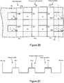
- Figure 2B shows a 2-cell layout of the three-transistor OTP memory cell of Figure 2A and illustrates how the bit lines of a memory cell array run in one direction (horizontally in the drawing) and the word lines (the gate electrodes) run in a direction perpendicular to the bit lines (vertically in the drawing).
- the two memory cells of Figure 2B are located one above the other in the drawing and gate electrodes 37A, 37B and 36 run vertically in the drawing.
- the gate electrode 37A separates the N+ source/drain regions 33A and 34; the gate electrode 36 separates the N+ source/drain regions 34 and 35; and the gate electrode 37B separates the N+ source/drain regions 35 and 33B.
- the shaded portions 43 represent STI (Shallow Trench Isolation) which electrically isolates the memory cells in the array.
- each memory cell is mirrored so that a second cell is also connected to a common bit line conducting plug.
- each conducting plug 40A is shared by a cell on each side of the vertical dashed line through the plugs, i.e., each of the memory cells shown in the drawing has a second memory cell (not shown) mirrored across the dashed vertical line.
- Figure 2C is a representative electrical circuit diagram of a three-transistor OTP memory cell. Access to the programmable element, the middle programming transistor, is provided by access transistors on either side of the programmable element. Both pass transistors have source/drain regions which are commonly connected to the same bit line and gate electrodes which are commonly connected to the same word line.
- the bit line (BL) is set low, at ground or negative voltage, and the WLr voltage on the gate electrodes is raised to turn on the pass transistor and the WLp voltage on the gate electrode of the programmable element is driven high. Both source/drain regions 34 and 35 are pulled to the BL voltage level through the two pass transistors. As a result, breakdown of the programming transistor gate oxide is more uniform across the entire channel. Moreover, the pass transistor drive current is doubled at a given WLr voltage when compared to the two-transistor cell and hard breakdown is more probable.
- a second advantage of the three-transistor cell is that a lower WLr voltage can be used during programming in order to pass the same program current. This can be significant if WLr voltage requires a voltage up-converter circuit.
- the three-transistor cells in a array will be much more uniform in terms of gate oxide thickness and quality, channel length and width, and other physical parameters of the program element, the central transistor.
- the isolated extension region 15 of the two-transistor OTP memory cell has a significant position dependence in an array and also variability across wafers, the width of the programmable element, the programming transistor, varies due to optical proximity effects and so does the gate oxide quality due to stress effects.
- the neighboring gate pitch change contributes to variations in gate dimension.
- the three-transistor OTP memory cell is absent of all these limitations and hence has better cell physical and electrical uniformity.
- the symmetric location of the two pass transistors with respect to the programming transistor improves the layout of the memory cells and a resulting uniformity in the manufactured cells of the array. Furthermore, the two pass transistors improve the programming results.
- the body region under the programming gate can be of the same conductivity type as that of source/drain regions 34 and 35.
- the programmable element MOSFET can be either an enhancement or depletion transistor.
Landscapes
- Semiconductor Memories (AREA)
- Non-Volatile Memory (AREA)
- Read Only Memory (AREA)
Abstract
Description
- This patent application claims the benefit of
U.S. Provisional Patent Application No. 62/348,732, filed June 10, 2016 - This invention relates to an improved OTP (One-Time Programmable) memory cell and, in particular, a three-transistor OTP memory cell with improved programmability.
- NVM (Nonvolatile memory) integrated circuits retain stored data even after power is removed. Such devices are found in many consumer electronics and industrial applications. A common memory cell in NVM integrated circuits is the antifuse memory cell based upon the programming of a gate dielectric layer. Such antifuse memory cells, more particularly, the one-time programmable (OTP) memory cell, are commonly used by integrated circuit designers since such cells are compatible with standard logic CMOS (Complementary Metal-Oxide-Semiconductor) process flows.
- An OTP memory cell includes a dielectric layer, such as the gate oxide, in a capacitor structure. The memory cell may include one or more select devices, such as a MOSFET (Metal-Oxide-Semiconductor-Field-Effect-Transistors), or a diode, such as a gated diode, to enable selective programming, the rupturing of the dielectric layer for an electrical connection, and reading of the memory cell. Each memory cell stores a bit of information, a "1" or a "0," depending on whether the cell has been programmed or not. A correspondence between a value of a bit and whether a cell is programmed may be defined arbitrarily. An array of such OTP memory cell includes the location of memory cells at cross points of orthogonal bit lines and word lines.
- Even though OTP memory cell arrays have been in use for many years, a persistent problem is the variability in the quality of the programmed connection in a memory cell. A significant portion of this variability can be attributed to layout-dependent effects on the program capacitor and the select device. That is, physical variations in the OTP memory cells adversely affect the post-programmed resistance and therefore the reading of the OTP memory cell state. A more robust antifuse OTP design is desired to improve the physical uniformity of the array memory cells and the distribution of the programmed cell read current.
- The present invention provides for an integrated circuit OTP (One-Time Programmable) memory cell comprising a programming MOSFET having source/drain regions; and two pass transistors symmetrically located with respect to the programming MOSFET and each pass transistor connected to one of the source/drain regions of the programming MOSFET; whereby programmability of the memory cell is enhanced. The two pass transistors comprise a first pass MOSFET and a second pass MOSFET. The first pass MOSFET has a gate electrode, and first and second source/drain regions in a substrate for the integrated circuit, the first source/drain region connected to a first conducting line, and the gate electrode controlling electrical connection between the first and second source/drain regions. The first pass MOSFET gate electrode is part of a second conducting line. The second pass MOSFET has a gate electrode, and third and fourth source/drain regions in the substrate for the integrated circuit, the fourth source/drain region connected to the first conducting line, and the gate electrode controlling electrical connection between the third and fourth source/drain regions. The second pass MOSFET gate electrode is connected to the second conducting line. The programming MOSFET comprises a gate electrode between the second and third source/drain region. Programmability of the OTP memory cell is enhanced.
- The present invention also provides for a method of programming an integrated circuit OTP memory cell. The memory cell has a programming MOSFET having two source/drain regions and a gate electrode over a channel region between the two source/drain regions. The method has the steps of accessing the two source/drain regions; driving the two source/drain regions to a first voltage; and driving the gate electrode to a second voltage to create a high voltage differential between the gate electrode and the two source/drain regions. Programming of the OTP memory cell is improved.
- Other objects, features, and advantages of the present invention will become apparent upon consideration of the following detailed description and the accompanying drawings, in which like reference designations represent like features throughout the figures.
-
-
Figure 1A shows a top view of a current two-transistor OTP memory cell;Figures 1B and1C are representational cross-sectional side views of theFigure 1A memory cell manufactured with different semiconductor processes, Silicon-On-Insulator (SOI) and bulk with deep N-Well, respectively. -
Figure 2A is a cross-sectional side of a three-transistor OTP memory cell according to one embodiment of the present invention;Figure 2B is a topside view of theFigure 2A memory cell; andFigure 2C is a circuit diagram of theFigure 2A memory cell. -
Figure 1A is a top layout view of a current two-transistor OTP memory cell, which has a pass transistor and a programmable element, a second transistor. The two transistors are MOSFETs, each with a gate electrode over a channel region separating two source/drain regions. In theFigure 1A memory cell the pass or select transistor is formed by agate electrode 17 over a channel region which separates two N+ source/drain regions semiconductor body 12 of P-conductivity. A thin insulating oxide layer 19 (seeFigure 1B ), called a gate oxide and not shown in this top view, separates thebody 12 andN+ regions gate electrode 17. The two source/drain regions gate electrode 17 define a channel region on the top of thebody 12 for the pass transistor. The N+ source/drain region 13 is connected to a bit line above (not shown) by a conductingplug 20. - Besides the pass transistor, the N+ source/
drain region 14 also forms a source/drain region for the second MOSFET transistor, the programmable element. A second N+ source/drain region 15 is part of the second MOSFET transistor which has agate electrode 16 over a channel region which separates the two N+ source/drain region gate oxide layer 18 separates thebody 12 andN+ regions gate electrode 16. The two source/drain regions gate electrode 16 define a channel region on the top of thebody 12 for the programmable element. Thegate electrodes electrodes - Various semiconductor processes can be used to manufacture the memory cell shown by the top view of
Figure 1A . One exemplary MOSFET process technology shown inFigure 1B is a SOI (Silicon-On-Insulator) process. Here the P-type body 12 rests on an insulating BOX (Body OXide)layer 11 which in turn rests on asemiconductor substrate 10. Another MOSFET process technology, shown inFigure 1C , provides for the N+ source/drain regions 13-15 of the MOSFET transistors to be formed in the P-type body, a P-well, which is located in a deep N-type well on a P-type substrate. The same reference numerals inFigure 1A are used for similar regions inFigures 1B and1C . Reverse-biased PN junctions provide electrical isolation for the bulk/body regions 12 inFigure 1C in contrast to the isolation provided to thebody regions 12 by theBOX layer 11 ofFigure 1B . Reference is made toU.S. Patent Nos. 7,471,540 and7,623,368 , both of which are assigned to the present assignee and incorporated by reference herein for all purposes, for further details of the different structures of the OTP memory cells which should not considered limitations of the present invention. The OTP memory cells can be formed by other semiconductor processes. - To program a memory cell, a voltage on the word line WLr turns on the pass transistor. A voltage on the bit line BL is driven low, ground or even negative, while a voltage on the programming element gate electrode, the word line WLp, is pulled high. The voltage for the programming element source/drain region opposite the pass transistor can be left floating. Some representative programming voltages are 0V for the bit line, +3.0V for the word line WLr, and +6.5V for the word line WLp. The goal of these voltages to create a high voltage differential between the
programming gate electrode 16 and the source/drain region 14 (or thebody 12 of the channel region of the programming element) so that thethin gate oxide 18 ruptures to create a conducting path between the gate electrode and the source/drain region 14. An unprogrammed memory cell has no conducting path. A bit of information is stored in the OTP memory cell as either a programmed or unprogrammed cell, i.e., whether there is a connection between the WLp and the source/drain region 14 or not. - A recurring problem for OTP cells is the quality of the programmed connection, or more precisely, the variation in the quality of the programmed connection. Gate oxide breakdown can vary widely with unwelcome decreased conductivity and large variations in the conductivity of the memory cells of an array. That is, the programmed connection can be electrically weak so that it is difficult to determine or read the state of the bit, i.e., 1 or 0, stored in the cell. Or even if when the bit can be read, the time interval to read the state of the bit is undesirably long. This variation of the programmed connection quality is attributed to microscopic anomalies or irregularities in the manufactured cell. Hence there have been many different approaches, such as described in the patents cited above, for improvements to lessen the variations in the gate oxide breakdown. Nonetheless, despite the improved programming results, continued improvements in the programmed connections are highly desirable.
- The present invention provides for a three-transistor OTP memory cell for further advancements for the OTP memory cell.
Figure 2A is a cross-sectional view of a three-transistor OTP memory cell, according to one embodiment of the present invention. It should be noted thatFigure 2A is drawn in a less stylized manner than that ofFigures 1B and1C . The three-transistor OTP memory cell has two pass transistors and a programmable element, a third transistor, between the two pass transistors. As in the case of the two-transistor OTP memory cell, the transistors are MOSFETs, each with a gate electrode over a channel region separating two source/drain regions. - The pass transistor on the right of the drawing is formed by a
gate electrode 37A over a channel region separating two N+ source/drain regions semiconductor body 31 of P-conductivity on asubstrate 30. A thin insulatingoxide layer 39A, the gate oxide separates thebody 12 andN+ regions gate electrode 37A. The two source/drain regions gate electrode 37A define a channel region on the top of thebody 12 for the pass transistor. The N+ source/drain region 33A is connected to a bit line above (not shown) by a conductingplug 40A and thegate electrode 37A is part of a word line WLr for accessing the OTP memory cell. - Besides the pass transistor, the N+ source/
drain region 34 also forms a source/drain region for the middle MOSFET transistor, the programmable element. A second N+ source/drain region 35 is part of the middle MOSFET transistor which has agate electrode 36 over a channel region separating the two N+ source/drain regions gate oxide layer 38 separates thebody 12 andN+ regions gate electrode 36. The two source/drain regions gate electrode 36 define a channel region on the top of thebody 12 for the programmable element. Thegate electrode 36 is part of a word line WLp for programming the OTP memory cell. - The pass transistor on the left of the drawing is formed by a
gate electrode 37B over a channel region separating two N+ source/drain regions oxide layer 39B, the gate oxide separates thebody 12 andN+ regions gate electrode 37B, and the two source/drain regions gate electrode 37B define a channel region on the top of thebody 12 for the left pass transistor. Thegate electrode 37B is part of the word line WLr for accessing the OTP memory cell. Also, the N+ source/drain region 33B is connected to the bit line above (not shown) by a conductingplug 40B, i.e., both source/drain regions Figure 2A the word lines run perpendicularly to the surface of the drawing. It should be understood that different semiconductor processes may be used for the three-transistor OTP memory cell. -
Figure 2B shows a 2-cell layout of the three-transistor OTP memory cell ofFigure 2A and illustrates how the bit lines of a memory cell array run in one direction (horizontally in the drawing) and the word lines (the gate electrodes) run in a direction perpendicular to the bit lines (vertically in the drawing). The two memory cells ofFigure 2B are located one above the other in the drawing andgate electrodes gate electrode 37A separates the N+ source/drain regions gate electrode 36 separates the N+ source/drain regions gate electrode 37B separates the N+ source/drain regions shaded portions 43 represent STI (Shallow Trench Isolation) which electrically isolates the memory cells in the array. In this particular layout of a three-transistor OTP memory cell array, each memory cell is mirrored so that a second cell is also connected to a common bit line conducting plug. InFigures 2A and2B each conductingplug 40A is shared by a cell on each side of the vertical dashed line through the plugs, i.e., each of the memory cells shown in the drawing has a second memory cell (not shown) mirrored across the dashed vertical line. -
Figure 2C is a representative electrical circuit diagram of a three-transistor OTP memory cell. Access to the programmable element, the middle programming transistor, is provided by access transistors on either side of the programmable element. Both pass transistors have source/drain regions which are commonly connected to the same bit line and gate electrodes which are commonly connected to the same word line. - To program the three-transistor OTP memory cell, the bit line (BL) is set low, at ground or negative voltage, and the WLr voltage on the gate electrodes is raised to turn on the pass transistor and the WLp voltage on the gate electrode of the programmable element is driven high. Both source/
drain regions - From a comparison of the layouts of
Figure 1A andFigure 2B , it is apparent that the three-transistor cells in a array will be much more uniform in terms of gate oxide thickness and quality, channel length and width, and other physical parameters of the program element, the central transistor. Because theisolated extension region 15 of the two-transistor OTP memory cell (seeFigure 1A ) has a significant position dependence in an array and also variability across wafers, the width of the programmable element, the programming transistor, varies due to optical proximity effects and so does the gate oxide quality due to stress effects. In addition, the neighboring gate pitch change contributes to variations in gate dimension. In contrast, the three-transistor OTP memory cell is absent of all these limitations and hence has better cell physical and electrical uniformity. Hence the symmetric location of the two pass transistors with respect to the programming transistor improves the layout of the memory cells and a resulting uniformity in the manufactured cells of the array. Furthermore, the two pass transistors improve the programming results. - This description of the invention has been presented for the purposes of illustration and description. It is not intended to be exhaustive or to limit the invention to the precise form described, and many modifications and variations are possible in light of the teaching above. The embodiments were chosen and described in order to best explain the principles of the invention and its practical applications. This description will enable others skilled in the art to best utilize and practice the invention in various embodiments and with various modifications as are suited to a particular use. As an example, the body region under the programming gate can be of the same conductivity type as that of source/
drain regions
Claims (12)
- An integrated circuit OTP (One-Time Programmable) memory cell comprising:a programming MOSFET having source/drain regions; andtwo pass transistors symmetrically located with respect to the programming MOSFET and each pass transistor connected to one of the source/drain regions of the programming MOSFET;whereby programmability of the memory cell is enhanced.
- The OTP memory cell of claim 1 wherein the two pass transistors comprise:a first pass MOSFET having a gate electrode, and first and second source/drain regions in a substrate for the integrated circuit, the first source/drain region connected to a first conducting line, and the gate electrode controlling electrical connection between the first and second source/drain regions, the gate electrode part of a second conducting line;a second pass MOSFET having a gate electrode, and third and fourth source/drain regions in the substrate for the integrated circuit, the fourth source/drain region connected to the first conducting line, and the gate electrode controlling electrical connection between the third and fourth source/drain regions, the gate electrode connected to the second conducting line; and wherein the programming MOSFET comprises:a gate electrode between the second and third source/drain regions.
- The OTP memory cell of claim 1 wherein the first conducting line comprises a bit line, the second and third conducting line comprises word lines for respectively accessing and programming the memory cell.
- The OTP memory cell of claim 1 wherein the first and second source/drain regions comprise N+ semiconductor regions.
- The OTP memory cell of claim 1 wherein the second and third conducting lines comprise material selected from the group comprising doped polysilicon, tungsten and tantalum, and silicides of metal and polysilicon,
- A method of programming an integrated circuit OTP memory cell, the memory cell having a programming MOSFET having two source/drain regions and a gate electrode over a channel region between the two source/drain regions, the method comprising:accessing the two source/drain regions;driving the two source/drain regions to a first voltage; anddriving the gate electrode to a second voltage to create a high voltage differential between the gate electrode and the two source/drain regions;whereby programming of the OTP memory cell is improved.
- The programming method of claim 6 wherein the two source/drain regions accessing step comprises:turning on two pass transistors, each pass transistor connected to one of the two source/drain regions and a first conducting line.
- The programming method of claim 7 wherein the two source/drains driving step comprises:driving the first conducting line to the first voltage.
- The programming method of claim 6 wherein each of the pass transistors comprises a pass MOSFET, each pass MOSFET having a gate electrode over a channel region separating a first and second source/drain regions, the first source/drain region connected to the first conducting line, the second source/drain region comprising one of the two source/drains of the programming MOSFET and the gate electrode comprising a second conducting line, the method comprising:placing a voltage on the gate electrode of each of the pass MOSFET to turn on the pass MOSFET to connect each of the two programming MOSFET source/drain regions to the first conducting line; anddriving the first conducting line to the first voltage.
- The programming method of claim 9 wherein the OTP memory cell is part of a memory cell array having a plurality of bit lines, a plurality of first word lines and a plurality of second word lines, and wherein one of the plurality of bit lines comprises the first conducting line, one of the plurality of first word lines comprises the second conducting line of a pass MOSFET, and one of the plurality of second word lines comprises the programming MOSFET gate electrode, the method comprising:placing the voltage on each of the first word lines for each of the pass MOSFETs to turn on the pass MOSFET to connect each of the two programming MOSFET source/drain regions to the one of a plurality of bit lines; anddriving the one of a plurality of bit lines to the first voltage; anddriving the one of a plurality of second word lines to the second voltage to create a high voltage differential between the gate electrode and the two source/drain regions of the programming MOSFET.
- An integrated circuit memory cell array comprising:a plurality of first parallel conducting lines;a plurality of second parallel conducting lines perpendicular to the first parallel conducting lines;a plurality of third parallel conducting lines perpendicular to the first parallel conducting lines;a plurality of memory cells, each memory cell located at the intersection of a first parallel conducting line and a pair of second parallel conducting lines and a third parallel conducting line, each memory cell having:a first pass MOSFET having a gate electrode, and first and second source/drain regions in a substrate for the integrated circuit, the first source/drain region connected to the first parallel conducting line, and the gate electrode controlling electrical connection between the first and second source/drain regions, the gate electrode part of one of the pair of second parallel conducting lines;a second pass MOSFET having a gate electrode, and third and fourth source/drain regions in the substrate for the integrated circuit, the fourth source/drain region connected to the first parallel conducting line, and the gate electrode controlling electrical connection between the third and fourth source/drain regions, the gate electrode part of the other of the pair of second parallel conducting lines; anda programming MOSFET having a gate electrode between the second and third source/drain regions, the gate electrode part of the third parallel conducting lines;whereby programmability of the memory cell in the array is enhanced.
- The memory cell array of claim 11 wherein the plurality of first parallel conducting lines comprise bit lines, the plurality of second parallel conducting lines comprise accessing word lines, and the plurality of third parallel conducting lines comprise programming word lines in the array.
Applications Claiming Priority (1)
| Application Number | Priority Date | Filing Date | Title |
|---|---|---|---|
| US201662348732P | 2016-06-10 | 2016-06-10 |
Publications (1)
| Publication Number | Publication Date |
|---|---|
| EP3255670A1 true EP3255670A1 (en) | 2017-12-13 |
Family
ID=59055039
Family Applications (1)
| Application Number | Title | Priority Date | Filing Date |
|---|---|---|---|
| EP17175419.5A Pending EP3255670A1 (en) | 2016-06-10 | 2017-06-12 | Three-transistor otp memory cell |
Country Status (3)
| Country | Link |
|---|---|
| US (1) | US10032522B2 (en) |
| EP (1) | EP3255670A1 (en) |
| CN (1) | CN107492553B (en) |
Families Citing this family (5)
| Publication number | Priority date | Publication date | Assignee | Title |
|---|---|---|---|---|
| CN110277369B (en) | 2018-03-14 | 2021-02-09 | 联华电子股份有限公司 | A fuse structure of dynamic random access memory element |
| CN110416214B (en) * | 2018-04-28 | 2021-07-20 | 无锡华润上华科技有限公司 | OTP memory device, manufacturing method thereof, and electronic device |
| CN112687692B (en) * | 2020-12-31 | 2023-02-24 | 珠海创飞芯科技有限公司 | OTP (one time programmable) device structure, OTP memory and operation method thereof |
| CN115241181B (en) * | 2021-04-23 | 2025-09-16 | 联华电子股份有限公司 | One time programmable memory element |
| US12310008B2 (en) | 2022-01-10 | 2025-05-20 | Changxin Memory Technologies, Inc. | Semiconductor structure and method for manufacturing same |
Citations (6)
| Publication number | Priority date | Publication date | Assignee | Title |
|---|---|---|---|---|
| US20030071296A1 (en) * | 2001-10-17 | 2003-04-17 | Peng Jack Zezhong | Reprogrammable non-volatile memory using a breakdown phenomena in an ultra-thin dielectric |
| US20060221698A1 (en) * | 2005-03-02 | 2006-10-05 | Sanyo Electric Co., Ltd. | Nonvolatile semiconductor memory device and manufacturing method of the same |
| US20070030719A1 (en) * | 2005-08-05 | 2007-02-08 | Hoefler Alexander B | One time programmable memory and method of operation |
| US7471540B2 (en) | 2007-01-24 | 2008-12-30 | Kilopass Technology, Inc. | Non-volatile semiconductor memory based on enhanced gate oxide breakdown |
| KR101095730B1 (en) * | 2011-07-22 | 2011-12-21 | 권의필 | Anti-fuse based semiconductor memory device |
| US20120008364A1 (en) * | 2010-07-06 | 2012-01-12 | Maxchip Electronics Corp. | One time programmable memory and the manufacturing method and operation method thereof |
Family Cites Families (10)
| Publication number | Priority date | Publication date | Assignee | Title |
|---|---|---|---|---|
| US6798693B2 (en) * | 2001-09-18 | 2004-09-28 | Kilopass Technologies, Inc. | Semiconductor memory cell and memory array using a breakdown phenomena in an ultra-thin dielectric |
| US6777757B2 (en) * | 2002-04-26 | 2004-08-17 | Kilopass Technologies, Inc. | High density semiconductor memory cell and memory array using a single transistor |
| US6713839B2 (en) * | 2002-05-24 | 2004-03-30 | Airip | Antifuse structure with low resistance |
| US7031209B2 (en) * | 2002-09-26 | 2006-04-18 | Kilopass Technology, Inc. | Methods and circuits for testing programmability of a semiconductor memory cell and memory array using a breakdown phenomenon in an ultra-thin dielectric |
| JP2013232494A (en) * | 2012-04-27 | 2013-11-14 | Sony Corp | Storage element, semiconductor device and operation method of the same, and electronic equipment |
| US8837220B2 (en) * | 2013-01-15 | 2014-09-16 | United Microelectronics Corp. | Nonvolatile memory and manipulating method thereof |
| US20140198583A1 (en) * | 2013-01-17 | 2014-07-17 | Infineon Technologies Ag | Method and System for Reducing the Size of Nonvolatile Memories |
| KR102169197B1 (en) * | 2014-09-16 | 2020-10-22 | 에스케이하이닉스 주식회사 | Antifuse OTP memory cell and cell array having improved program efficiency |
| US9852805B2 (en) * | 2015-06-25 | 2017-12-26 | Kilopass Technology, Inc. | Write enhancement for one time programmable (OTP) semiconductors |
| US9634015B2 (en) * | 2015-08-18 | 2017-04-25 | Ememory Technology Inc. | Antifuse-type one time programming memory cell and array structure with same |
-
2017
- 2017-06-12 EP EP17175419.5A patent/EP3255670A1/en active Pending
- 2017-06-12 CN CN201710438733.7A patent/CN107492553B/en active Active
- 2017-06-12 US US15/620,657 patent/US10032522B2/en active Active
Patent Citations (7)
| Publication number | Priority date | Publication date | Assignee | Title |
|---|---|---|---|---|
| US20030071296A1 (en) * | 2001-10-17 | 2003-04-17 | Peng Jack Zezhong | Reprogrammable non-volatile memory using a breakdown phenomena in an ultra-thin dielectric |
| US20060221698A1 (en) * | 2005-03-02 | 2006-10-05 | Sanyo Electric Co., Ltd. | Nonvolatile semiconductor memory device and manufacturing method of the same |
| US20070030719A1 (en) * | 2005-08-05 | 2007-02-08 | Hoefler Alexander B | One time programmable memory and method of operation |
| US7471540B2 (en) | 2007-01-24 | 2008-12-30 | Kilopass Technology, Inc. | Non-volatile semiconductor memory based on enhanced gate oxide breakdown |
| US7623368B2 (en) | 2007-01-24 | 2009-11-24 | Kilopass Technology, Inc. | Non-volatile semiconductor memory based on enhanced gate oxide breakdown |
| US20120008364A1 (en) * | 2010-07-06 | 2012-01-12 | Maxchip Electronics Corp. | One time programmable memory and the manufacturing method and operation method thereof |
| KR101095730B1 (en) * | 2011-07-22 | 2011-12-21 | 권의필 | Anti-fuse based semiconductor memory device |
Also Published As
| Publication number | Publication date |
|---|---|
| US10032522B2 (en) | 2018-07-24 |
| CN107492553A (en) | 2017-12-19 |
| CN107492553B (en) | 2023-12-15 |
| US20170358368A1 (en) | 2017-12-14 |
Similar Documents
| Publication | Publication Date | Title |
|---|---|---|
| US10347646B2 (en) | Anti-fuse cell structure including reading and programming devices with different gate dielectric thickness | |
| KR102178025B1 (en) | OTP Cell Having a Reduced Layout Area | |
| US8305790B2 (en) | Electrical anti-fuse and related applications | |
| US9589970B1 (en) | Antifuse one-time programmable memory | |
| CN108336058B (en) | semiconductor memory device | |
| CN101361139B (en) | One-time programmable memory and its operation method | |
| JP4981661B2 (en) | Split channel antifuse array structure | |
| US8957482B2 (en) | Electrical fuse and related applications | |
| US10032522B2 (en) | Three-transistor OTP memory cell | |
| CN104425513A (en) | Programmable memory | |
| US9899100B2 (en) | One time programmable (OTP) cell and an OTP memory array using the same | |
| KR101958518B1 (en) | OTP Cell Having Improved Programming Reliability | |
| US20210335804A1 (en) | Semiconductor structure and method for manufacturing the same | |
| US20250040133A1 (en) | Semiconductor integrated circuit device and method of providing bias power to the same | |
| CN109671710B (en) | OTP cell with improved programmability | |
| US9941017B1 (en) | Antifuse one-time programmable semiconductor memory | |
| CN120640681A (en) | One-time programmable memory cell | |
| CN121459894A (en) | One time programmable memory cell |
Legal Events
| Date | Code | Title | Description |
|---|---|---|---|
| PUAI | Public reference made under article 153(3) epc to a published international application that has entered the european phase |
Free format text: ORIGINAL CODE: 0009012 |
|
| STAA | Information on the status of an ep patent application or granted ep patent |
Free format text: STATUS: REQUEST FOR EXAMINATION WAS MADE |
|
| 17P | Request for examination filed |
Effective date: 20170612 |
|
| AK | Designated contracting states |
Kind code of ref document: A1 Designated state(s): AL AT BE BG CH CY CZ DE DK EE ES FI FR GB GR HR HU IE IS IT LI LT LU LV MC MK MT NL NO PL PT RO RS SE SI SK SM TR |
|
| AX | Request for extension of the european patent |
Extension state: BA ME |
|
| RAP1 | Party data changed (applicant data changed or rights of an application transferred) |
Owner name: SYNOPSYS, INC. |
|
| STAA | Information on the status of an ep patent application or granted ep patent |
Free format text: STATUS: EXAMINATION IS IN PROGRESS |
|
| 17Q | First examination report despatched |
Effective date: 20200911 |
|
| P01 | Opt-out of the competence of the unified patent court (upc) registered |
Effective date: 20230528 |