EP3255653A1 - Semiconductor crystal substrate, infrared detector, method for producing semiconductor crystal substrate, and method for producing infrared detector - Google Patents
Semiconductor crystal substrate, infrared detector, method for producing semiconductor crystal substrate, and method for producing infrared detector Download PDFInfo
- Publication number
- EP3255653A1 EP3255653A1 EP17165717.4A EP17165717A EP3255653A1 EP 3255653 A1 EP3255653 A1 EP 3255653A1 EP 17165717 A EP17165717 A EP 17165717A EP 3255653 A1 EP3255653 A1 EP 3255653A1
- Authority
- EP
- European Patent Office
- Prior art keywords
- layer
- gasb
- buffer layer
- substrate
- type
- Prior art date
- Legal status (The legal status is an assumption and is not a legal conclusion. Google has not performed a legal analysis and makes no representation as to the accuracy of the status listed.)
- Withdrawn
Links
Images








Classifications
-
- H—ELECTRICITY
- H10—SEMICONDUCTOR DEVICES; ELECTRIC SOLID-STATE DEVICES NOT OTHERWISE PROVIDED FOR
- H10F—INORGANIC SEMICONDUCTOR DEVICES SENSITIVE TO INFRARED RADIATION, LIGHT, ELECTROMAGNETIC RADIATION OF SHORTER WAVELENGTH OR CORPUSCULAR RADIATION
- H10F39/00—Integrated devices, or assemblies of multiple devices, comprising at least one element covered by group H10F30/00, e.g. radiation detectors comprising photodiode arrays
- H10F39/10—Integrated devices
- H10F39/103—Integrated devices the at least one element covered by H10F30/00 having potential barriers, e.g. integrated devices comprising photodiodes or phototransistors
-
- H—ELECTRICITY
- H10—SEMICONDUCTOR DEVICES; ELECTRIC SOLID-STATE DEVICES NOT OTHERWISE PROVIDED FOR
- H10F—INORGANIC SEMICONDUCTOR DEVICES SENSITIVE TO INFRARED RADIATION, LIGHT, ELECTROMAGNETIC RADIATION OF SHORTER WAVELENGTH OR CORPUSCULAR RADIATION
- H10F39/00—Integrated devices, or assemblies of multiple devices, comprising at least one element covered by group H10F30/00, e.g. radiation detectors comprising photodiode arrays
- H10F39/10—Integrated devices
- H10F39/107—Integrated devices having multiple elements covered by H10F30/00 in a repetitive configuration, e.g. radiation detectors comprising photodiode arrays
-
- H—ELECTRICITY
- H10—SEMICONDUCTOR DEVICES; ELECTRIC SOLID-STATE DEVICES NOT OTHERWISE PROVIDED FOR
- H10F—INORGANIC SEMICONDUCTOR DEVICES SENSITIVE TO INFRARED RADIATION, LIGHT, ELECTROMAGNETIC RADIATION OF SHORTER WAVELENGTH OR CORPUSCULAR RADIATION
- H10F71/00—Manufacture or treatment of devices covered by this subclass
- H10F71/127—The active layers comprising only Group III-V materials, e.g. GaAs or InP
- H10F71/1272—The active layers comprising only Group III-V materials, e.g. GaAs or InP comprising at least three elements, e.g. GaAlAs or InGaAsP
-
- H—ELECTRICITY
- H10—SEMICONDUCTOR DEVICES; ELECTRIC SOLID-STATE DEVICES NOT OTHERWISE PROVIDED FOR
- H10F—INORGANIC SEMICONDUCTOR DEVICES SENSITIVE TO INFRARED RADIATION, LIGHT, ELECTROMAGNETIC RADIATION OF SHORTER WAVELENGTH OR CORPUSCULAR RADIATION
- H10F77/00—Constructional details of devices covered by this subclass
- H10F77/10—Semiconductor bodies
- H10F77/12—Active materials
- H10F77/124—Active materials comprising only Group III-V materials, e.g. GaAs
- H10F77/1248—Active materials comprising only Group III-V materials, e.g. GaAs having three or more elements, e.g. GaAlAs, InGaAs or InGaAsP
-
- H—ELECTRICITY
- H10—SEMICONDUCTOR DEVICES; ELECTRIC SOLID-STATE DEVICES NOT OTHERWISE PROVIDED FOR
- H10F—INORGANIC SEMICONDUCTOR DEVICES SENSITIVE TO INFRARED RADIATION, LIGHT, ELECTROMAGNETIC RADIATION OF SHORTER WAVELENGTH OR CORPUSCULAR RADIATION
- H10F77/00—Constructional details of devices covered by this subclass
- H10F77/10—Semiconductor bodies
- H10F77/14—Shape of semiconductor bodies; Shapes, relative sizes or dispositions of semiconductor regions within semiconductor bodies
- H10F77/146—Superlattices; Multiple quantum well structures
-
- H—ELECTRICITY
- H10—SEMICONDUCTOR DEVICES; ELECTRIC SOLID-STATE DEVICES NOT OTHERWISE PROVIDED FOR
- H10P—GENERIC PROCESSES OR APPARATUS FOR THE MANUFACTURE OR TREATMENT OF DEVICES COVERED BY CLASS H10
- H10P14/00—Formation of materials, e.g. in the shape of layers or pillars
- H10P14/20—Formation of materials, e.g. in the shape of layers or pillars of semiconductor materials
- H10P14/22—Formation of materials, e.g. in the shape of layers or pillars of semiconductor materials using physical deposition, e.g. vacuum deposition or sputtering
-
- H—ELECTRICITY
- H10—SEMICONDUCTOR DEVICES; ELECTRIC SOLID-STATE DEVICES NOT OTHERWISE PROVIDED FOR
- H10P—GENERIC PROCESSES OR APPARATUS FOR THE MANUFACTURE OR TREATMENT OF DEVICES COVERED BY CLASS H10
- H10P14/00—Formation of materials, e.g. in the shape of layers or pillars
- H10P14/20—Formation of materials, e.g. in the shape of layers or pillars of semiconductor materials
- H10P14/29—Formation of materials, e.g. in the shape of layers or pillars of semiconductor materials characterised by the substrates
- H10P14/2901—Materials
- H10P14/2907—Materials being Group IIIA-VA materials
- H10P14/2911—Arsenides
-
- H—ELECTRICITY
- H10—SEMICONDUCTOR DEVICES; ELECTRIC SOLID-STATE DEVICES NOT OTHERWISE PROVIDED FOR
- H10P—GENERIC PROCESSES OR APPARATUS FOR THE MANUFACTURE OR TREATMENT OF DEVICES COVERED BY CLASS H10
- H10P14/00—Formation of materials, e.g. in the shape of layers or pillars
- H10P14/20—Formation of materials, e.g. in the shape of layers or pillars of semiconductor materials
- H10P14/29—Formation of materials, e.g. in the shape of layers or pillars of semiconductor materials characterised by the substrates
- H10P14/2901—Materials
- H10P14/2907—Materials being Group IIIA-VA materials
- H10P14/2912—Antimonides
-
- H—ELECTRICITY
- H10—SEMICONDUCTOR DEVICES; ELECTRIC SOLID-STATE DEVICES NOT OTHERWISE PROVIDED FOR
- H10P—GENERIC PROCESSES OR APPARATUS FOR THE MANUFACTURE OR TREATMENT OF DEVICES COVERED BY CLASS H10
- H10P14/00—Formation of materials, e.g. in the shape of layers or pillars
- H10P14/20—Formation of materials, e.g. in the shape of layers or pillars of semiconductor materials
- H10P14/32—Formation of materials, e.g. in the shape of layers or pillars of semiconductor materials characterised by intermediate layers between substrates and deposited layers
- H10P14/3202—Materials thereof
- H10P14/3214—Materials thereof being Group IIIA-VA semiconductors
- H10P14/3222—Antimonides
-
- H—ELECTRICITY
- H10—SEMICONDUCTOR DEVICES; ELECTRIC SOLID-STATE DEVICES NOT OTHERWISE PROVIDED FOR
- H10P—GENERIC PROCESSES OR APPARATUS FOR THE MANUFACTURE OR TREATMENT OF DEVICES COVERED BY CLASS H10
- H10P14/00—Formation of materials, e.g. in the shape of layers or pillars
- H10P14/20—Formation of materials, e.g. in the shape of layers or pillars of semiconductor materials
- H10P14/32—Formation of materials, e.g. in the shape of layers or pillars of semiconductor materials characterised by intermediate layers between substrates and deposited layers
- H10P14/3242—Structure
- H10P14/3244—Layer structure
- H10P14/3251—Layer structure consisting of three or more layers
- H10P14/3252—Alternating layers, e.g. superlattice
-
- H—ELECTRICITY
- H10—SEMICONDUCTOR DEVICES; ELECTRIC SOLID-STATE DEVICES NOT OTHERWISE PROVIDED FOR
- H10P—GENERIC PROCESSES OR APPARATUS FOR THE MANUFACTURE OR TREATMENT OF DEVICES COVERED BY CLASS H10
- H10P14/00—Formation of materials, e.g. in the shape of layers or pillars
- H10P14/20—Formation of materials, e.g. in the shape of layers or pillars of semiconductor materials
- H10P14/34—Deposited materials, e.g. layers
- H10P14/3402—Deposited materials, e.g. layers characterised by the chemical composition
- H10P14/3414—Deposited materials, e.g. layers characterised by the chemical composition being group IIIA-VIA materials
- H10P14/3422—Antimonides
-
- H—ELECTRICITY
- H10—SEMICONDUCTOR DEVICES; ELECTRIC SOLID-STATE DEVICES NOT OTHERWISE PROVIDED FOR
- H10P—GENERIC PROCESSES OR APPARATUS FOR THE MANUFACTURE OR TREATMENT OF DEVICES COVERED BY CLASS H10
- H10P14/00—Formation of materials, e.g. in the shape of layers or pillars
- H10P14/20—Formation of materials, e.g. in the shape of layers or pillars of semiconductor materials
- H10P14/34—Deposited materials, e.g. layers
- H10P14/3438—Doping during depositing
- H10P14/3441—Conductivity type
- H10P14/3442—N-type
-
- H—ELECTRICITY
- H10—SEMICONDUCTOR DEVICES; ELECTRIC SOLID-STATE DEVICES NOT OTHERWISE PROVIDED FOR
- H10P—GENERIC PROCESSES OR APPARATUS FOR THE MANUFACTURE OR TREATMENT OF DEVICES COVERED BY CLASS H10
- H10P14/00—Formation of materials, e.g. in the shape of layers or pillars
- H10P14/20—Formation of materials, e.g. in the shape of layers or pillars of semiconductor materials
- H10P14/34—Deposited materials, e.g. layers
- H10P14/3438—Doping during depositing
- H10P14/3441—Conductivity type
- H10P14/3444—P-type
Definitions
- An aspect of this disclosure relates to a semiconductor crystal substrate, an infrared detector, a method for producing the semiconductor crystal substrate, and a method for producing the infrared detector.
- infrared detectors comprised of semiconductor materials.
- An example of such an infrared detector has a configuration where an infrared absorption layer with an InAs/GaSb superlattice structure is formed on a GaSb substrate.
- the InAs/GaSb superlattice structure forming the infrared absorption layer is a type-II superlattice (T2SL) structure and has a type-II band lineup.
- an infrared detector that is sensitive in a wavelength range from a middle wave (MW) infrared wavelength of 3-5 ⁇ m to a long wave (LW) infrared wavelength of 8-10 ⁇ m.
- a PIN-type infrared detector with a T2SL structure uses interband optical absorption. For this reason, it is expected that a PIN-type infrared detector with a T2SL structure will have improved temperature characteristics compared with a quantum dot infrared photodetector (QDIP) and a quantum well infrared photodetector (QWIP) that use intersubband optical absorption.
- QDIP quantum dot infrared photodetector
- QWIP quantum well infrared photodetector
- Such a PIN-type infrared detector with a T2SL structure is desired to have high light sensitivity and a low dark current in addition to improved temperature characteristics.
- M. Lee et al., Journal of Applied Physics 59, 2895 (1986 ) proposes improving the quality of a GaSb buffer layer by changing the growth temperature and the V/III ratio in molecular beam epitaxy (MBE).
- M. Lee et al., Journal of Applied Physics 59, 2895 (1986 ) discloses that an excellent GaSb layer can be formed by performing epitaxial growth at a growth temperature between 500 °C and 550 °C and with a V/III ratio between 5 and 10.
- a semiconductor crystal substrate including a GaSb layer with a highly-flat surface.
- a semiconductor crystal substrate including a crystal substrate that is formed of a material including one of GaSb and InAs, a first buffer layer that is formed on the crystal substrate and formed of a material including GaSb, and a second buffer layer that is formed on the first buffer layer and formed of a material including GaSb.
- the first buffer layer has a p-type conductivity
- the second buffer layer has an n-type conductivity.
- SSMBE solid source molecular beam epitaxy
- FIG. 2 is an AFM image of the surface of the GaSb substrate 11 after the oxide film is removed.
- the surface of the GaSb substrate 11 becomes uneven.
- Measured surface roughness (RMS) of the surface of the GaSb substrate 11, from which the oxide film was removed, was 3.1 nm.
- the measurement range of surface roughness (RMS) was 1 ⁇ m x 1 ⁇ m (which also applies to the measurement of surface roughness of GaSb layers described later).
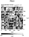
- FIG. 3 is an AFM image of a surface of the GaSb layer 12a formed under this condition.
- the surface roughness (RMS) of the GaSb layer 12a was 0.13 nm.
- the GaSb layer 12b with a thickness of 500 nm was formed by MBE at a substrate temperature of 440 °C on the GaSb substrate 11 from which the oxide film was removed.
- FIG. 4 is an AFM image of a surface of the GaSb layer 12b formed under this condition.
- the surface roughness (RMS) of the GaSb layer 12b was 0.16 nm.
- the GaSb layer 12b is not as flat as the GaSb layer 12a formed at the substrate temperature of 520 °C, the surface of the GaSb substrate 11 or the semiconductor crystal substrate can also be planarized by forming the GaSb layer 12b.
- pits or dents are formed in the surface of the GaSb layer 12a formed at the substrate temperature of 520 °C.
- the pits are relatively deep, have a depth of several nm, and exist at a density of about 10 9 cm -2 .
- an infrared absorption layer with a T2SL structure is formed on the GaSb layer 12a having pits in its surface, dislocations and defects tend to be formed in the infrared absorption layer due to the pits. This in turn may reduce the light sensitivity and increase the dark current of an infrared detector.
- no pit is formed in the surface of the GaSb layer 12b formed at the substrate temperature of 440 °C.
- the surface roughness of the GaSb layer 12b is greater than the surface roughness of the GaSb layer 12a formed at the substrate temperature of 520 °C.
- the conductivity of the GaSb layer 12a and the GaSb layer 12b formed at different substrate temperatures was examined. As a result of the examination, it was found out that the GaSb layer 12a formed by MBE at the substrate temperature of 520 °C had p-type conductivity, and the GaSb layer 12b formed by MBE at the substrate temperature of 440 °C had n-type conductivity. Also, the carrier concentrations in the GaSb layer 12a formed at the substrate temperature of 520 °C and the GaSb layer 12b formed at the substrate temperature of 440 °C were measured by using a capacitance-voltage (CV) technique.
- CV capacitance-voltage
- the carrier concentration in the GaSb layer 12a was about 1 ⁇ 10 18 cm -3
- the carrier concentration in the GaSb layer 12b was about 4 ⁇ 10 18 cm -3
- the GaSb layer 12a and the GaSb layer 12b were analyzed by secondary ion mass spectrometry (SIMS), and it was found out that the concentration of an impurity element (dopant) in each of the GaSb layer 12a and the GaSb layer 12b was less than or equal to 1 ⁇ 10 17 cm -3 .
- the above results indicate that Sb is easily removed from a formed GaSb layer when the substrate temperature is high, and the amount of Ga is slightly greater than the amount of Sb in the GaSb layer 12a formed by MBE at the substrate temperature of 520 °C. Accordingly, it is assumed that a part of Ga enters the site of Sb in the GaSb crystal and as a result, the GaSb layer 12a exhibits p-type conductivity.
- the above results also indicate that the removal of Sb from a formed GaSb layer is suppressed when the substrate temperature is low, and the amount of Sb is slightly greater than the amount of Ga in the GaSb layer 12b formed by MBE at the substrate temperature of 440 °C. Accordingly, it is assumed that a part of Sb enters the site of Ga in the GaSb crystal and as a result, the GaSb layer 12b exhibits n-type conductivity.
- the substrate temperature during the formation of a GaSb layer is high, the movement of Ga atoms due to surface migration becomes active.
- the substrate temperature is low, the movement of Ga atoms due to surface migration becomes less active. Accordingly, it is assumed that the distance of movement of Ga atoms due to surface migration becomes long in the GaSb layer 12a formed at the substrate temperature of 520 °C and as a result, the surface of the GaSb layer 12a becomes flatter than the surface of the GaSb layer 12b formed at the substrate temperature of 440 °C.
- the composition ratio of Ga is high, Ga tends to form clusters. Accordingly, it can be considered that the pits in the surface of the GaSb layer 12a formed at the substrate temperature of 520 °C are formed at the boundaries between the clusters.
- the GaSb layer 12a formed at the substrate temperature of 520 °C becomes rich in Ga, this Ga enters the site of Sb and functions as an acceptor, and as a result, the GaSb layer 12a exhibits p-type conductivity.
- the GaSb layer 12a formed at a high substrate temperature has low surface roughness (RMS) and high flatness. However, pits tend to be formed in the GaSb layer 12a due to a high composition ratio of Ga.
- the GaSb layer 12b formed at the substrate temperature of 440°C becomes rich in Sb, this Sb enters the site of Ga and functions as a donor, and as a result, the GaSb layer 12b exhibits n-type conductivity.
- the GaSb layer 12b formed at a lower substrate temperature has slightly higher surface roughness (RMS). However, no pit is formed in the GaSb layer 12b because the composition ratio of Ga is low.
- the semiconductor crystal substrate of the first embodiment includes a GaSb substrate 111 that is a crystal substrate, a p-type first GaSb layer 112 formed on the GaSb substrate 111, and an n-type second GaSb layer 113 formed on the first GaSb layer 112. More specifically, the first GaSb layer 112 is formed under the same condition as the GaSb layer 12a, i.e., formed by MBE at a substrate temperature of 520 °C after an oxide film is removed from the surface of the GaSb substrate 111.
- the second GaSb layer 113 is formed under the same condition as the GaSb layer 12b, i.e., formed by MBE at a substrate temperature of 440 °C.
- the GaSb substrate 111 is substantially the same as the GaSb substrate 11.
- FIG. 6 is an AFM image of a surface of the second GaSb layer 113 formed on the first GaSb layer 112 as described above.
- the first GaSb layer 112 is formed at a substrate temperature of 520 °C and has a thickness of 100 nm.
- the second GaSb layer 113 is formed at a substrate temperature of 440 °C and has a thickness of 400 nm.
- the surface of the second GaSb layer 113 is flat with a surface roughness (RMS) of 0.10 nm, and no pit as in FIG. 3 is formed in the surface of the second GaSb layer 113.
- RMS surface roughness
- the first GaSb layer 112 is formed at a high substrate temperature of 520 °C, the first GaSb layer 112 becomes rich in Ga and although pits are formed, the first GaSb layer 112 becomes mostly flat.
- the second GaSb layer 113 is formed on the first GaSb layer 112 at a low substrate temperature of 440 °C, the second GaSb layer 113 becomes rich in Sb and no pit is formed in the surface of the second GaSb layer 113. Also, it is assumed that atoms moved due to surface migration fill the pits.
- the surface roughness (RMS) of the second GaSb layer 113 becomes 0.10 nm that is less than the surface roughness (RMS) 0.13 nm of the GaSb layer 12a formed at the surface temperature of 520 °C and the surface roughness (RMS) 0.16 nm of the GaSb layer 12b formed at the surface temperature of 440 °C.
- the concentration of an impurity element (dopant) in each of the GaSb layer 112 and the GaSb layer 113 is less than or equal to 1 ⁇ 10 17 cm -3 and is substantially the same as that in the GaSb layer 12a and the GaSb layer 12b.
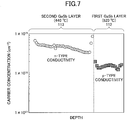
- FIG. 7 is a drawing illustrating carrier concentrations in the GaSb layer 112 and the GaSb layer 113 of the semiconductor crystal substrate of the present embodiment.
- the carrier concentrations were measured by a CV technique while etching the semiconductor crystal substrate in the depth direction.
- the first GaSb layer 112 has p-type conductivity and has a carrier concentration of about 1 ⁇ 10 18 cm -3
- the second GaSb layer 113 has n-type conductivity and has a carrier concentration of about 4 ⁇ 10 18 cm -3 .
- FIG. 8 is an AFM image of a surface of a test sample including the GaSb substrate 111, a first GaSb film formed on the GaSb substrate 111 by MBE at a substrate temperature of 520 °C after removing an oxide film from the surface of the GaSb substrate 111, and a second GaSb film formed on the first GaSb film by MBE at a substrate temperature of 470 °C.
- the surface roughness (RMS) of the second GaSb film of the test sample is 0.18 nm, carriers of the second GaSb film have p-type conductivity, and the carrier concentration of the second GaSb film is about 5 ⁇ 10 18 cm -3 . Thus, the surface roughness (RMS) of this test sample is not low enough.
- FIG. 9 is an AFM image of a surface of a test sample including the GaSb substrate 111, a first GaSb film formed on the GaSb substrate 111 by MBE at a substrate temperature of 520 °C after removing an oxide film from the surface of the GaSb substrate 111, and a second GaSb film formed on the first GaSb film by MBE at a substrate temperature of 410 °C.
- the surface roughness (RMS) of the second GaSb film of the test sample is 0.13 nm, carriers of the second GaSb film have n-type conductivity, and the carrier concentration of the second GaSb film is about 4 ⁇ 10 18 cm -3 .
- the surface roughness (RMS) of this test sample is also not low enough.
- the carrier concentration in each of the first GaSb layer 112 having p-type conductivity and the second GaSb layer 113 having n-type conductivity is preferably greater than or equal to 1 ⁇ 10 18 cm -3 and less than or equal to 1 ⁇ 10 20 cm -3 .
- the first GaSb layer 112 with such a carrier concentration can be formed by solid source molecular beam epitaxy (SSMBE) at a substrate temperature greater than or equal to 500 °C and less than or equal to 550 °C.
- the second GaSb layer 113 with such a carrier concentration can be formed by solid source molecular beam epitaxy (SSMBE) at a substrate temperature greater than or equal to 420 °C and less than or equal to 460 °C.
- the semiconductor crystal substrate of the present embodiment includes the GaSb substrate 111 that is a crystal substrate, the first GaSb layer 112 formed on the GaSb substrate 111, and the second GaSb layer 113 formed on the first GaSb layer 112.
- the first GaSb layer 112 is rich in Ga and has p-type conductivity
- the second GaSb layer 113 is rich in Sb and has n-type conductivity.
- the first GaSb layer 112 may be referred to as a first buffer layer
- the second GaSb layer 113 may be referred to as a second buffer layer.
- each of the first buffer layer and the second buffer layer may be formed of Ga 1-x In x As 1-y Sb y (0 ⁇ x ⁇ 0.1, 0 ⁇ y ⁇ 1). More specifically, each of the first buffer layer and the second buffer layer may be formed of GaInSb, GaAsSb, or GaInAsSb that is a material including In and/or As in addition to GaSb.
- an exemplary method for producing a semiconductor crystal substrate according to the present embodiment is described with reference to FIGs. 10A through 10C .
- an n-type GaSb (001) substrate used as the GaSb substrate 111 is placed in a vacuum chamber of a solid source molecular beam epitaxy (SSMBE) apparatus.
- the GaSb substrate 111 is heated by a heater.
- the substrate temperature of the GaSb substrate 111 reaches 400 °C
- a surface of the GaSb substrate 111 is irradiated with an Sb beam.
- the beam flux of Sb is, for example, 5.0 ⁇ 10 -7 Torr.
- the GaSb substrate 111 When the GaSb substrate 111 is heated further, an oxide film of GaSb formed on the surface of the GaSb substrate 111 is removed at a substrate temperature of around 500 °C. Then, in a state where the Sb beam is being emitted, the GaSb substrate 111 is heated up to a substrate temperature of 530 °C and is kept in this state for 20 minutes to completely remove the oxide film of GaSb formed on the surface of the GaSb substrate 111.
- the first GaSb layer 112 used as a first buffer layer is formed on the GaSb substrate 111. Specifically, in a state where the GaSb substrate 111 is at the substrate temperature of 520 °C and the Sb beam is being emitted, a Ga beam is also emitted to form the first GaSb layer 112.
- the beam flux of Ga is, for example, 5.0 ⁇ 10 -8 Torr, and the V/III ratio is 10. Under these conditions, the growth rate of the first GaSb layer 112 is 0.30 ⁇ m/h. Film forming is performed for about 20 minutes until the thickness of the first GaSb layer 112 reaches 100 nm, and then the Ga beam is stopped.
- the first GaSb layer 112 formed at a substrate temperature of 520 °C as described above has p-type conductivity.
- the second GaSb layer 113 used as a second buffer layer is formed on the first GaSb layer 112 used as the first buffer layer.
- the substrate temperature is dropped to 440 °C and the Ga beam is emitted again to form the second GaSb layer 113.
- the beam flux of Ga is, for example, 5.0 ⁇ 10 -8 Torr, and the V/III ratio is 10.
- the growth rate of the second GaSb layer 113 is 0.30 ⁇ m/h.
- Film forming is performed for about 80 minutes until the thickness of the second GaSb layer 113 reaches 400 nm, and then the Ga beam is stopped.
- the second GaSb layer 113 formed at a substrate temperature of 440 °C as described above has n-type conductivity.
- the semiconductor crystal substrate of the present embodiment is produced.
- an n-type GaSb substrate is used as the GaSb substrate 111 in the present embodiment
- a p-type GaSb substrate may also be used as the GaSb substrate 111.
- the plane direction of the GaSb substrate 111 is not limited to (001), and an off substrate may also be used as the GaSb substrate 111.
- an InAs substrate may be used in place of the GaSb substrate 111.
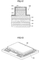
- FIG. 11 illustrates an example of a configuration of the infrared detector of the second embodiment
- FIG. 12 is an enlarged view of a part of the infrared detector corresponding to a pixel.
- the infrared detector of the second embodiment includes a GaSb substrate 111, a first GaSb layer 112 formed on the GaSb substrate 111, a second GaSb layer 113 formed on the first GaSb layer 112, a p-type contact layer 114 formed on the second GaSb layer 113, an infrared absorption layer 115 formed on the p-type contact layer 114, and an n-type contact layer 116 formed on the infrared absorption layer 115.
- the GaSb substrate 111 is an n-type GaSb (001) substrate, the first GaSb layer 112 has a thickness of about 100 nm, and the second GaSb layer 113 has a thickness of about 400 nm.
- the p-type contact layer 114 is a p-type GaSb layer that has a thickness of 500 nm and is doped with Be as an impurity element.
- the infrared absorption layer 115 has an InAs/GaSb superlattice (T2SL) structure. Specifically, the infrared absorption layer 115 is formed by alternately stacking an InAs layer with a thickness of about 2 nm and a GaSb layer with a thickness of about 2 nm.
- the infrared absorption layer 115 includes 200 pairs of the InAs layer and the GaSb layer, and has a thickness of about 800 nm.
- the n-type contact layer 116 is an n-type InAs layer that has a thickness of about 30 nm and is doped with Si as an impurity element.
- the p-type contact layer 114 may be referred to as a first contact layer
- the n-type contact layer 116 may be referred to as a second contact layer.
- Pixel separating grooves 120 are formed in the n-type contact layer 116 and the infrared absorption layer 115 to separate pixels of the infrared detector.
- a passivation film 131 composed of SiN is formed on the side surfaces and the bottom surfaces of the pixel separating grooves 120.
- multiple pixels separated by the pixel separating grooves 120 are arranged two-dimensionally.
- An electrode 141 is formed on the n-type contact layer 116 of each of the pixels separated by the pixel separating grooves 120, and an electrode 142 is formed on the p-type contact layer 114.
- the infrared absorption layer 115 and the n-type contact layer 116 near the electrode 142 form a wiring support 143.
- a wiring layer 144 is formed to extend from the electrode 142, via the side surface of the wiring support 143, to the upper surface of the wiring support 143. Accordingly, the infrared absorption layer 115 and the n-type contact layer 116 forming the wiring support 143 are not used for infrared detection.
- Each of the electrodes 141 and 142 is formed of a metal multilayer film of Ti, Pt, and Au.
- a structure or a device with the above configuration may be referred to as an infrared detector or an infrared detecting device 150.
- the infrared detector of the present embodiment can detect infrared radiation that enters from the back side of the GaSb substrate 111.
- the infrared detector of the present embodiment has a configuration where a signal reading circuit device 160 is connected to the infrared detecting device 150.
- bumps 145 are formed on the electrodes 141 of the infrared detecting device 150
- a bump 146 is formed on the wiring layer 144 of the infrared detecting device 150.
- the signal reading circuit device 160 includes a circuit board 161 on which a signal reading circuit(s) is formed. Electrodes 162 are formed on the circuit board 161, and bumps 163 are formed on the electrodes 162. The bumps 145 and 146 and the bumps 163 are formed to face each other.
- the infrared detecting device 150 and the signal reading circuit device 160 are connected to each other by connecting the bumps 145 and 146 with the corresponding bumps 163.
- FIG. 13 is a perspective view of the infrared detector of the present embodiment.
- FIGs. 14A through 17B An exemplary method for producing an infrared detector according to the second embodiment is described with reference to FIGs. 14A through 17B .
- the infrared detector of the second embodiment can be produced by using the semiconductor crystal substrate of the first embodiment.
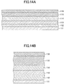
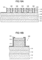
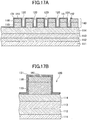
- FIGs. 14A , 15A , 16A , and 17A illustrates the whole of a structure relevant to the corresponding step
- each of FIGs. 14B , 15B , 16B , and 17B is an enlarged view of a part of the structure corresponding to a pixel.
- the first GaSb layer 112, the second GaSb layer 113, the p-type contact layer 114, the infrared absorption layer 115, and the n-type contact layer 116 are epitaxially grown in this order on the GaSb substrate 111 by MBE.
- a structure obtained by sequentially forming the first GaSb layer 112 and the second GaSb layer 113 on the GaSb substrate 111 corresponds to the semiconductor crystal substrate of the first embodiment. Therefore, detailed descriptions of the GaSb substrate 111, the first GaSb layer 112, and the second GaSb layer 113 are omitted here.
- the first GaSb layer 112 and the second GaSb layer 113 are sequentially formed on the GaSb substrate 111, and the p-type contact layer 114 is formed on the second GaSb layer 113.
- the p-type contact layer 114 is a p-type GaSb layer that is formed by emitting Ga, Sb, and Be beams.
- the temperature of the Be cell is adjusted so that the concentration of Be that is an impurity element used as a dopant of the p-type contact layer 114 becomes 5.0 ⁇ 10 18 cm -3 .
- the beam flux of Ga is 5.0 ⁇ 10 -8 Torr
- the beam flux of Sb is 5.0 ⁇ 10 -7 Torr
- the V/III ratio is 10. Under these conditions, the growth rate of GaSb is 0.30 ⁇ m/h. Film forming is performed for about 100 minutes until the thickness of the p-type contact layer 114 reaches 500 nm, and then the Be and Ga beams are stopped.
- the infrared absorption layer 115 with an InAs/GaSb superlattice structure is formed on the p-type contact layer 114. Specifically, the Sb beam is stopped, and In and As beams are emitted. In this step, the beam flux of In is 5.0 ⁇ 10 -8 Torr, the beam flux of As is 5.0 ⁇ 10 -7 Torr, and the V/III ratio is 10. Under these conditions, the growth rate of InAs is 0.30 ⁇ m/h. Film forming is performed for about 36 seconds until the thickness of an InAs layer reaches 2 nm, and then the In and As beams are stopped. Next, after an interval of three seconds, Ga and Sb beams are emitted.
- the beam flux of Ga is 5.0 ⁇ 10 -8 Torr
- the beam flux of Sb is 5.0 ⁇ 10 -7 Torr
- the V/III ratio is 10.
- the growth rate of GaSb is 0.30 ⁇ m/h.
- Film forming is performed for about 36 seconds until the thickness of a GaSb layer reaches 2 nm, and then the Ga and Sb beams are stopped. After an interval of three seconds, the above steps are repeated.
- the cycle is repeated 200 times to form the infrared absorption layer 115 with a total thickness of about 800 nm.
- the n-type contact layer 116 is formed on the infrared absorption layer 115.
- the n-type contact layer 116 is an n-type InAs layer that is formed by emitting In, As, and Si beams.
- the temperature of the Si cell is adjusted so that the concentration of Si that is an impurity element used as a dopant of the n-type contact layer 116 becomes 5.0 ⁇ 10 18 cm -3 .
- the beam flux of In is 5.0 ⁇ 10 -8 Torr
- the beam flux of As is 5.0 ⁇ 10 -7 Torr
- the V/III ratio is 10. Under these conditions, the growth rate of InAs is 0.30 ⁇ m/h. Film forming is performed for about 6 minutes until the thickness of an InAs layer reaches 30 nm, and then the In and Si beams are stopped.
- the substrate temperature is dropped to 400 °C. Then, the As beam is stopped, and a structure where epitaxial films are formed on the GaSb substrate 111 is taken out of the vacuum chamber of the MBE apparatus.
- portions of the n-type contact layer 116 and the infrared absorption layer 115 are removed to form the pixel separating grooves 120.
- a photoresist is applied to the n-type contact layer 116, and the photoresist is exposed and developed by an exposure apparatus to form a resist pattern (not shown) having openings in areas where the pixel separating grooves 120 are to be formed.
- portions of the n-type contact layer 116 and the infrared absorption layer 115 in the areas not covered by the resist pattern are removed by dry etching using a CF 4 gas to form the pixel separating grooves 120.
- pixels having a mesa structure and separated by the pixel separating grooves 120 are formed.
- the size of each pixel is 50 ⁇ m x 50 ⁇ m, and 256 x 256 pixels are formed in the infrared detector.
- the passivation film 131 is formed on the upper surface of the n-type contact layer 116 and the side surfaces of the n-type contact layer 116 and the infrared absorption layer 115 forming each pixel, and on the upper surface of the p-type contact layer 114 between pixels.
- the passivation film 131 is an SiN film with a thickness of 100 nm and is formed by plasma chemical vapor deposition (CVD) using SiH 4 and NH 3 gases.
- a photoresist is applied to the structure of FIG. 16A , and the photoresist is exposed and developed by an exposure apparatus to form a resist pattern (not shown) having openings in areas where the electrodes 141 and 142 are to be formed. Then, portions of the passivation film 131 in the areas not covered by the resist pattern are removed by dry etching using a CF 4 gas to expose portions of the n-type contact layer 116 and the p-type contact layer 114 in those areas.
- the electrodes 141 are formed on the exposed portions of the n-type contact layer 116 and the electrode 142 is formed on the exposed portion of the p-type contact layer 114.
- a resist pattern (not shown) is formed to have openings in areas where the electrodes 141 and 142 are to be formed.
- a metal multilayer film made of Ti, Pt, and Au is formed by vacuum deposition or sputtering, and the metal multilayer film is immersed in, for example, an organic solvent to remove, together with the resist pattern, portions of the metal multilayer film on the resist pattern by a lift-off technique. The remaining portions of the metal multilayer film form the electrodes 141 on the n-type contact layer 116 and the electrode 142 on the p-type contact layer 114.
- the wiring layer 144 is formed on the electrode 142 and the side and upper surfaces of the wiring support 143, the bumps 145 are formed on the electrodes 141, and the bump 146 is formed on a portion of the wiring layer 144 above the wiring support 143.
- the formed bumps 145 and 146 are connected with the bumps 163 of the signal reading circuit device 160 by flip-chip bonding. As a result, the infrared detecting device 150 and the signal reading circuit device 160 are connected to each other.
- FIG. 18 illustrates an exemplary configuration of the semiconductor laser of the third embodiment.
- the semiconductor laser of the third embodiment includes the semiconductor crystal substrate of the first embodiment where the first GaSb layer 112 and the second GaSb layer 113 are sequentially formed on the GaSb substrate 111.
- the semiconductor laser also includes a p-type GaSb cladding layer 221, a multi-quantum well (MQW) layer 222, an n-type GaSb cladding layer 223, and an n-type InAs layer 224 that are formed on the second GaSb layer 113 in this order.
- the p-type GaSb cladding layer 221 has a thickness of about 500 nm and is doped with Be as a p-type impurity element.
- the MQW layer 222 is formed by alternately stacking a GaSb layer with a thickness of about 5 nm and an InAs layer with a thickness of about 5 nm.
- the MQW layer 222 includes 20 pairs of the GaSb layer and the InAs layer.
- the n-type GaSb cladding layer 223 has a thickness of about 100 nm, is doped with Si as an n-type impurity element, and has a carrier concentration of 5.0 ⁇ 10 18 cm -3 .
- the n-type InAs layer 224 has a thickness of about 30 nm.
- portions of the n-type InAs layer 224, the n-type GaSb cladding layer 223, and the MQW layer 222 are removed to form a mesa structure 230.
- portions of the n-type InAs layer 224, the n-type GaSb cladding layer 223, and the MQW layer 222 are removed by dry etching using a CF 4 gas as an etching gas to expose portions of the p-type GaSb cladding layer 221 and thereby form the mesa structure 230.
- lower electrodes 241 are formed on the exposed portions of the p-type GaSb cladding layer 221, and an upper electrode 242 is formed on the upper surface of the n-type InAs layer 224.
- Each of the lower electrodes 241 and the upper electrode 242 is formed of, for example, a metal multilayer film of Ti, Pt, and Au.
- the GaSb substrate 111 is cleaved to form a stripe-shaped piece having a width of 20 ⁇ m and a length of 50 ⁇ m.
- the semiconductor laser of the present embodiment is produced.
- the semiconductor laser is an edge emitting laser with a wavelength of 3.0 ⁇ m.
- FIG. 19 illustrates an exemplary configuration of the light emitting diode of the fourth embodiment.
- the light emitting diode of the fourth embodiment includes the semiconductor crystal substrate of the first embodiment. Similarly to the third embodiment, after the p-type GaSb cladding layer 221, the MQW layer 222, the n-type GaSb cladding layer 223, and the n-type InAs layer 224 are epitaxially grown on the second GaSb layer 113 by MBE, the lower electrode 241 and the upper electrode 242 are formed.
- the GaSb substrate 111 is cleaved to form a chip having a width of 50 ⁇ m and a length of 50 ⁇ m.
- the light emitting diode of the fourth embodiment is produced.
- the light emitting diode emits light from the side on which the n-type InAs layer 224 is formed. Accordingly, the area of the n-type InAs layer 224 where the upper electrode 242 is not present is preferably as large as possible.
- FIG. 20 illustrates an exemplary configuration of the field effect transistor of the fifth embodiment.
- the field effect transistor of the fifth embodiment includes the semiconductor crystal substrate of the first embodiment where the first GaSb layer 112 and the second GaSb layer 113 are sequentially formed on the GaSb substrate 111.
- An Al 0.8 Ga 0.2 Sb layer 251 and a channel layer 252 are sequentially formed by MBE on the second GaSb layer 113.
- the thickness of the Al 0.8 Ga 0.2 Sb layer 251 is about 2 nm.
- the channel layer 252 is a p-type In 0.2 Ga 0.8 Sb layer with a thickness of 5 nm, is doped with Be as a p-type impurity element, and has a carrier concentration of 5.0 ⁇ 10 18 cm -3 .
- an insulating film 260 is formed by atomic layer deposition (ALD) on the channel layer 252.
- the insulating film 260 is an Al 2 O 3 film with a thickness of 3 nm.
- a gate electrode 271 is formed on the insulating film 260, and a source electrode 272 and a drain electrode 273 are formed on the channel layer 252.
- the gate electrode 271 may be a tungsten (W) film with a thickness of about 100 nm, and may be formed by CVD on the insulating layer 260.
- the gate electrode 271 is formed to have a gate length of 30 nm.
- portions of the insulating film 260 which correspond to areas where the source electrode 272 and the drain electrode 273 are to be formed, are removed. Then, the source electrode 272 and the drain electrode 273 are formed in the areas with, for example, Ni films.
- thermoelectric transducer produced by using the semiconductor crystal substrate of the first embodiment is described.
- the thermoelectric transducer of the sixth embodiment is described below with reference to FIGs. 21 and 22 .
- the thermoelectric transducer of the sixth embodiment includes the semiconductor crystal substrate of the first embodiment where the first GaSb layer 112 and the second GaSb layer 113 are sequentially formed on the GaSb substrate 111.
- a superlattice layer 280 and a cap layer 281 are sequentially formed by MBE on the second GaSb layer 113.
- the superlattice layer 280 is formed by alternately stacking a GaSb layer with a thickness of about 5 nm and an InAs layer with a thickness of about 5 nm.
- the superlattice layer 280 includes 500 pairs of the GaSb layer and the InAs layer.
- the cap layer 281 is a non-doped InAs film with a thickness of 30 nm.
- portions of the cap layer 281, the superlattice layer 280, the second GaSb layer 113, and the first GaSb layer 112 are removed to form mesa structures 282.
- portions of the cap layer 281, the superlattice layer 280, the second GaSb layer 113, and the first GaSb layer 112 are removed by dry etching using a CF 4 gas as an etching gas to form the mesa structures 282.
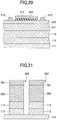
- FIG. 21 illustrates a resulting structure.
- an SiO 2 film 283 is formed to fill a gap between the mesa structures 282.
- the back side of the GaSb substrate 111 is ground by chemical mechanical polishing (CMP) to reduce the thickness of the GaSb substrate 111 to about 3 ⁇ m.
- CMP chemical mechanical polishing
- n-type and p-type dopants are ion-implanted into the mesa structures 282 and activation annealing is performed to form n-type regions (n-type elements) and p-type regions (p-type elements).
- electrodes 290 are formed on the ends of the n-type elements and the p-type elements such that the n-type elements and the p-type elements are connected in series.
- Each of the electrodes 290 is formed of, for example, a metal multilayer film of Ti, Pt, and Au.
- An aspect of this disclosure makes it possible to provide a semiconductor crystal substrate including a GaSb layer with a highly-flat surface.
Landscapes
- Physical Deposition Of Substances That Are Components Of Semiconductor Devices (AREA)
- Light Receiving Elements (AREA)
- Crystals, And After-Treatments Of Crystals (AREA)
- Physical Vapour Deposition (AREA)
- Recrystallisation Techniques (AREA)
- Photometry And Measurement Of Optical Pulse Characteristics (AREA)
Abstract
Description
- An aspect of this disclosure relates to a semiconductor crystal substrate, an infrared detector, a method for producing the semiconductor crystal substrate, and a method for producing the infrared detector.
- There exist infrared detectors comprised of semiconductor materials. An example of such an infrared detector has a configuration where an infrared absorption layer with an InAs/GaSb superlattice structure is formed on a GaSb substrate. The InAs/GaSb superlattice structure forming the infrared absorption layer is a type-II superlattice (T2SL) structure and has a type-II band lineup. Accordingly, by adjusting the film thickness and the period of the superlattice of the InAs/GaSb superlattice structure, it is possible to obtain an infrared detector that is sensitive in a wavelength range from a middle wave (MW) infrared wavelength of 3-5 µm to a long wave (LW) infrared wavelength of 8-10 µm.
- A PIN-type infrared detector with a T2SL structure uses interband optical absorption. For this reason, it is expected that a PIN-type infrared detector with a T2SL structure will have improved temperature characteristics compared with a quantum dot infrared photodetector (QDIP) and a quantum well infrared photodetector (QWIP) that use intersubband optical absorption. Such a PIN-type infrared detector with a T2SL structure is desired to have high light sensitivity and a low dark current in addition to improved temperature characteristics.
- To obtain a PIN-type infrared detector using a T2SL structure and having high light sensitivity and a low dark current, it is necessary to form a high-quality T2SL crystal in the infrared absorption layer. Also, to form a high-quality T2SL crystal, it is necessary to form a GaSb buffer layer with high flatness below the infrared absorption layer (see, for example, Japanese Laid-Open Patent Publication No.
2015-109388 03-129721 - However, it is not possible to form a high-quality T2SL crystal that fully satisfies the desired characteristics of an infrared absorption layer by just forming a GaSb buffer layer under various conditions. Accordingly, there is a demand for a semiconductor crystal substrate including a GaSb buffer layer with a highly-flat surface.
- Accordingly, it is an object in one aspect of the embodiment to provide a semiconductor crystal substrate including a GaSb layer with a highly-flat surface.
- According to an aspect of the invention, there is provided a semiconductor crystal substrate including a crystal substrate that is formed of a material including one of GaSb and InAs, a first buffer layer that is formed on the crystal substrate and formed of a material including GaSb, and a second buffer layer that is formed on the first buffer layer and formed of a material including GaSb. The first buffer layer has a p-type conductivity, and the second buffer layer has an n-type conductivity.
-
-
FIG. 1 is a drawing illustrating an exemplary structure of a semiconductor crystal substrate where a GaSb layer is formed on a GaSb substrate; -
FIG. 2 is a drawing illustrating an AFM image of a surface of a GaSb substrate; -
FIG. 3 is a drawing illustrating an AFM image of a surface of a GaSb layer formed on a GaSb substrate at a substrate temperature of 520 °C; -
FIG. 4 is a drawing illustrating an AFM image of a surface of a GaSb layer formed on a GaSb substrate at a substrate temperature of 440 °C; -
FIG. 5 is a drawing illustrating an exemplary structure of a semiconductor crystal substrate according to a first embodiment; -
FIG. 6 is a drawing illustrating an AFM image of a surface of a GaSb layer of a semiconductor crystal substrate according to the first embodiment; -
FIG. 7 is a drawing illustrating carrier concentrations in GaSb layers of a semiconductor crystal substrate according to the first embodiment; -
FIG. 8 is a drawing illustrating an AFM image of a surface of a second GaSb layer formed at a temperature of 470 °C; -
FIG. 9 is a drawing illustrating an AFM image of a surface of a second GaSb layer formed at a temperature of 410 °C; -
FIGs. 10A through 10C are drawings illustrating a method for producing a semiconductor crystal substrate according to the first embodiment; -
FIG. 11 is a drawing illustrating an example of a configuration of an infrared detector according to a second embodiment; -
FIG. 12 is an enlarged view of a part of the infrared detector ofFIG. 11 ; -
FIG. 13 is a perspective view of the infrared detector ofFIG. 11 ; -
FIGs. 14A and 14B are drawings illustrating steps of a method for producing an infrared detector according to the second embodiment; -
FIGs. 15A and 15B are drawings illustrating steps of the method for producing the infrared detector according to the second embodiment; -
FIGs. 16A and 16B are drawings illustrating steps of the method for producing the infrared detector according to the second embodiment; -
FIGs. 17A and 17B are drawings illustrating steps of the method for producing the infrared detector according to the second embodiment; -
FIG. 18 is a drawing illustrating an example of a configuration of a semiconductor laser according to a third embodiment; -
FIG. 19 is a drawing illustrating an example of a configuration of a light-emitting diode according to a fourth embodiment; -
FIG. 20 is a drawing illustrating an example of a configuration of a field-effect transistor according to a fifth embodiment; -
FIG. 21 is a drawing illustrating a thermoelectric transducer according to a sixth embodiment; and -
FIG. 22 is another drawing illustrating the thermoelectric transducer according to the sixth embodiment. - Embodiments of the present invention are described below with reference to the accompanying drawings. The same reference numbers are assigned to the same components throughout the drawings, and repeated descriptions of those components are omitted.
- The inventors studied the relationship between film-forming conditions and flatness of a GaSb film. Specifically, as illustrated by
FIG. 1 , semiconductor crystal substrates were prepared by forming aGaSb layer 12a and aGaSb layer 12b under different film-forming conditions on aGaSb substrate 11, and the flatness of surfaces of theGaSb layer 12a and theGaSb layer 12b was measured. The flatness of the surfaces of theGaSb layer 12a and theGaSb layer 12b was measured using an atomic force microscope (AFM). Each of theGaSb layer 12a and theGaSb layer 12b was formed by solid source molecular beam epitaxy (SSMBE) at a V/III ratio of about 10. - An oxide film formed on a surface of the
GaSb substrate 11 was removed by heating theGaSb substrate 11 at a temperature of about 500 °C in vacuum.FIG. 2 is an AFM image of the surface of theGaSb substrate 11 after the oxide film is removed. As indicated byFIG. 2 , when the oxide film is removed from the surface of theGaSb substrate 11 made of a semiconductor crystal, the surface of theGaSb substrate 11 becomes uneven. Measured surface roughness (RMS) of the surface of theGaSb substrate 11, from which the oxide film was removed, was 3.1 nm. The measurement range of surface roughness (RMS) was 1 µm x 1 µm (which also applies to the measurement of surface roughness of GaSb layers described later). - Next, the
GaSb layer 12a with a thickness of 500 nm was formed by MBE at a substrate temperature of 520 °C on theGaSb substrate 11 from which the oxide film was removed.FIG. 3 is an AFM image of a surface of theGaSb layer 12a formed under this condition. The surface roughness (RMS) of theGaSb layer 12a was 0.13 nm. Thus, the surface of theGaSb substrate 11 or the semiconductor crystal substrate can be planarized by forming theGaSb layer 12a. - Also, the
GaSb layer 12b with a thickness of 500 nm was formed by MBE at a substrate temperature of 440 °C on theGaSb substrate 11 from which the oxide film was removed.FIG. 4 is an AFM image of a surface of theGaSb layer 12b formed under this condition. The surface roughness (RMS) of theGaSb layer 12b was 0.16 nm. Thus, although theGaSb layer 12b is not as flat as theGaSb layer 12a formed at the substrate temperature of 520 °C, the surface of theGaSb substrate 11 or the semiconductor crystal substrate can also be planarized by forming theGaSb layer 12b. - Here, as can be seen in
FIG. 3 , pits or dents are formed in the surface of theGaSb layer 12a formed at the substrate temperature of 520 °C. The pits are relatively deep, have a depth of several nm, and exist at a density of about 109 cm-2. When an infrared absorption layer with a T2SL structure is formed on theGaSb layer 12a having pits in its surface, dislocations and defects tend to be formed in the infrared absorption layer due to the pits. This in turn may reduce the light sensitivity and increase the dark current of an infrared detector. - On the other hand, as can be seen in
FIG. 4 , no pit is formed in the surface of theGaSb layer 12b formed at the substrate temperature of 440 °C. However, the surface roughness of theGaSb layer 12b is greater than the surface roughness of theGaSb layer 12a formed at the substrate temperature of 520 °C. - Next, the conductivity of the
GaSb layer 12a and theGaSb layer 12b formed at different substrate temperatures was examined. As a result of the examination, it was found out that theGaSb layer 12a formed by MBE at the substrate temperature of 520 °C had p-type conductivity, and theGaSb layer 12b formed by MBE at the substrate temperature of 440 °C had n-type conductivity. Also, the carrier concentrations in theGaSb layer 12a formed at the substrate temperature of 520 °C and theGaSb layer 12b formed at the substrate temperature of 440 °C were measured by using a capacitance-voltage (CV) technique. The carrier concentration in theGaSb layer 12a was about 1×1018 cm-3, and the carrier concentration in theGaSb layer 12b was about 4×1018 cm-3. Further, theGaSb layer 12a and theGaSb layer 12b were analyzed by secondary ion mass spectrometry (SIMS), and it was found out that the concentration of an impurity element (dopant) in each of theGaSb layer 12a and theGaSb layer 12b was less than or equal to 1×1017 cm-3. - The above results indicate that Sb is easily removed from a formed GaSb layer when the substrate temperature is high, and the amount of Ga is slightly greater than the amount of Sb in the
GaSb layer 12a formed by MBE at the substrate temperature of 520 °C. Accordingly, it is assumed that a part of Ga enters the site of Sb in the GaSb crystal and as a result, theGaSb layer 12a exhibits p-type conductivity. The above results also indicate that the removal of Sb from a formed GaSb layer is suppressed when the substrate temperature is low, and the amount of Sb is slightly greater than the amount of Ga in theGaSb layer 12b formed by MBE at the substrate temperature of 440 °C. Accordingly, it is assumed that a part of Sb enters the site of Ga in the GaSb crystal and as a result, theGaSb layer 12b exhibits n-type conductivity. - Here, when the substrate temperature during the formation of a GaSb layer is high, the movement of Ga atoms due to surface migration becomes active. On the other hand, when the substrate temperature is low, the movement of Ga atoms due to surface migration becomes less active. Accordingly, it is assumed that the distance of movement of Ga atoms due to surface migration becomes long in the
GaSb layer 12a formed at the substrate temperature of 520 °C and as a result, the surface of theGaSb layer 12a becomes flatter than the surface of theGaSb layer 12b formed at the substrate temperature of 440 °C. Also, it is known that when the composition ratio of Ga is high, Ga tends to form clusters. Accordingly, it can be considered that the pits in the surface of theGaSb layer 12a formed at the substrate temperature of 520 °C are formed at the boundaries between the clusters. - Thus, the
GaSb layer 12a formed at the substrate temperature of 520 °C becomes rich in Ga, this Ga enters the site of Sb and functions as an acceptor, and as a result, theGaSb layer 12a exhibits p-type conductivity. TheGaSb layer 12a formed at a high substrate temperature has low surface roughness (RMS) and high flatness. However, pits tend to be formed in theGaSb layer 12a due to a high composition ratio of Ga. - On the other hand, the
GaSb layer 12b formed at the substrate temperature of 440°C becomes rich in Sb, this Sb enters the site of Ga and functions as a donor, and as a result, theGaSb layer 12b exhibits n-type conductivity. Compared with theGaSb layer 12a formed at the substrate temperature of 520 °C, theGaSb layer 12b formed at a lower substrate temperature has slightly higher surface roughness (RMS). However, no pit is formed in theGaSb layer 12b because the composition ratio of Ga is low. - A semiconductor crystal substrate according to a first embodiment is obtained based on the above findings. As illustrated by
FIG. 5 , the semiconductor crystal substrate of the first embodiment includes aGaSb substrate 111 that is a crystal substrate, a p-typefirst GaSb layer 112 formed on theGaSb substrate 111, and an n-typesecond GaSb layer 113 formed on thefirst GaSb layer 112. More specifically, thefirst GaSb layer 112 is formed under the same condition as theGaSb layer 12a, i.e., formed by MBE at a substrate temperature of 520 °C after an oxide film is removed from the surface of theGaSb substrate 111. Also, thesecond GaSb layer 113 is formed under the same condition as theGaSb layer 12b, i.e., formed by MBE at a substrate temperature of 440 °C. Here, theGaSb substrate 111 is substantially the same as theGaSb substrate 11. -
FIG. 6 is an AFM image of a surface of thesecond GaSb layer 113 formed on thefirst GaSb layer 112 as described above. Thefirst GaSb layer 112 is formed at a substrate temperature of 520 °C and has a thickness of 100 nm. Thesecond GaSb layer 113 is formed at a substrate temperature of 440 °C and has a thickness of 400 nm. As illustrated inFIG. 6 , the surface of thesecond GaSb layer 113 is flat with a surface roughness (RMS) of 0.10 nm, and no pit as inFIG. 3 is formed in the surface of thesecond GaSb layer 113. - Possible reasons why a film having a flat surface with not pit can be formed are explained below. First, because the
first GaSb layer 112 is formed at a high substrate temperature of 520 °C, thefirst GaSb layer 112 becomes rich in Ga and although pits are formed, thefirst GaSb layer 112 becomes mostly flat. Second, because thesecond GaSb layer 113 is formed on thefirst GaSb layer 112 at a low substrate temperature of 440 °C, thesecond GaSb layer 113 becomes rich in Sb and no pit is formed in the surface of thesecond GaSb layer 113. Also, it is assumed that atoms moved due to surface migration fill the pits. These are assumed to be the reasons why the surface roughness (RMS) of thesecond GaSb layer 113 becomes 0.10 nm that is less than the surface roughness (RMS) 0.13 nm of theGaSb layer 12a formed at the surface temperature of 520 °C and the surface roughness (RMS) 0.16 nm of theGaSb layer 12b formed at the surface temperature of 440 °C. The concentration of an impurity element (dopant) in each of theGaSb layer 112 and theGaSb layer 113 is less than or equal to 1×1017 cm-3 and is substantially the same as that in theGaSb layer 12a and theGaSb layer 12b.FIG. 7 is a drawing illustrating carrier concentrations in theGaSb layer 112 and theGaSb layer 113 of the semiconductor crystal substrate of the present embodiment. The carrier concentrations were measured by a CV technique while etching the semiconductor crystal substrate in the depth direction. As illustrated inFIG. 7 , thefirst GaSb layer 112 has p-type conductivity and has a carrier concentration of about 1×1018 cm-3, and thesecond GaSb layer 113 has n-type conductivity and has a carrier concentration of about 4×1018 cm-3. -
FIG. 8 is an AFM image of a surface of a test sample including theGaSb substrate 111, a first GaSb film formed on theGaSb substrate 111 by MBE at a substrate temperature of 520 °C after removing an oxide film from the surface of theGaSb substrate 111, and a second GaSb film formed on the first GaSb film by MBE at a substrate temperature of 470 °C. The surface roughness (RMS) of the second GaSb film of the test sample is 0.18 nm, carriers of the second GaSb film have p-type conductivity, and the carrier concentration of the second GaSb film is about 5×1018 cm-3. Thus, the surface roughness (RMS) of this test sample is not low enough. -
FIG. 9 is an AFM image of a surface of a test sample including theGaSb substrate 111, a first GaSb film formed on theGaSb substrate 111 by MBE at a substrate temperature of 520 °C after removing an oxide film from the surface of theGaSb substrate 111, and a second GaSb film formed on the first GaSb film by MBE at a substrate temperature of 410 °C. The surface roughness (RMS) of the second GaSb film of the test sample is 0.13 nm, carriers of the second GaSb film have n-type conductivity, and the carrier concentration of the second GaSb film is about 4×1018 cm-3. Thus, the surface roughness (RMS) of this test sample is also not low enough. - In the present embodiment, the carrier concentration in each of the
first GaSb layer 112 having p-type conductivity and thesecond GaSb layer 113 having n-type conductivity is preferably greater than or equal to 1×1018 cm-3 and less than or equal to 1×1020 cm-3. Thefirst GaSb layer 112 with such a carrier concentration can be formed by solid source molecular beam epitaxy (SSMBE) at a substrate temperature greater than or equal to 500 °C and less than or equal to 550 °C. Also, thesecond GaSb layer 113 with such a carrier concentration can be formed by solid source molecular beam epitaxy (SSMBE) at a substrate temperature greater than or equal to 420 °C and less than or equal to 460 °C. - As described above, the semiconductor crystal substrate of the present embodiment includes the
GaSb substrate 111 that is a crystal substrate, thefirst GaSb layer 112 formed on theGaSb substrate 111, and thesecond GaSb layer 113 formed on thefirst GaSb layer 112. Thefirst GaSb layer 112 is rich in Ga and has p-type conductivity, and thesecond GaSb layer 113 is rich in Sb and has n-type conductivity. In the present application, thefirst GaSb layer 112 may be referred to as a first buffer layer, and thesecond GaSb layer 113 may be referred to as a second buffer layer. - Also in the present embodiment, each of the first buffer layer and the second buffer layer may be formed of Ga1-xInxAs1-ySby (0 ≦ x ≦ 0.1, 0 ≦ y < 1). More specifically, each of the first buffer layer and the second buffer layer may be formed of GaInSb, GaAsSb, or GaInAsSb that is a material including In and/or As in addition to GaSb.
- Next, an exemplary method for producing a semiconductor crystal substrate according to the present embodiment is described with reference to
FIGs. 10A through 10C . First, as illustrated byFIG. 10A , an n-type GaSb (001) substrate used as theGaSb substrate 111 is placed in a vacuum chamber of a solid source molecular beam epitaxy (SSMBE) apparatus. Next, theGaSb substrate 111 is heated by a heater. When the substrate temperature of theGaSb substrate 111reaches 400 °C, a surface of theGaSb substrate 111 is irradiated with an Sb beam. The beam flux of Sb is, for example, 5.0×10⁻⁷ Torr. When theGaSb substrate 111 is heated further, an oxide film of GaSb formed on the surface of theGaSb substrate 111 is removed at a substrate temperature of around 500 °C. Then, in a state where the Sb beam is being emitted, theGaSb substrate 111 is heated up to a substrate temperature of 530 °C and is kept in this state for 20 minutes to completely remove the oxide film of GaSb formed on the surface of theGaSb substrate 111. - Next, as illustrated by
FIG. 10B , thefirst GaSb layer 112 used as a first buffer layer is formed on theGaSb substrate 111. Specifically, in a state where theGaSb substrate 111 is at the substrate temperature of 520 °C and the Sb beam is being emitted, a Ga beam is also emitted to form thefirst GaSb layer 112. In this step, the beam flux of Ga is, for example, 5.0×10⁻⁸ Torr, and the V/III ratio is 10. Under these conditions, the growth rate of thefirst GaSb layer 112 is 0.30 µm/h. Film forming is performed for about 20 minutes until the thickness of thefirst GaSb layer 112 reaches 100 nm, and then the Ga beam is stopped. Thefirst GaSb layer 112 formed at a substrate temperature of 520 °C as described above has p-type conductivity. - Next, as illustrated by
FIG. 10C , thesecond GaSb layer 113 used as a second buffer layer is formed on thefirst GaSb layer 112 used as the first buffer layer. Specifically, in a state where the Sb beam is being emitted, the substrate temperature is dropped to 440 °C and the Ga beam is emitted again to form thesecond GaSb layer 113. In this step, the beam flux of Ga is, for example, 5.0×10⁻⁸ Torr, and the V/III ratio is 10. Under these conditions, the growth rate of thesecond GaSb layer 113 is 0.30 µm/h. Film forming is performed for about 80 minutes until the thickness of thesecond GaSb layer 113reaches 400 nm, and then the Ga beam is stopped. Thesecond GaSb layer 113 formed at a substrate temperature of 440 °C as described above has n-type conductivity. - Through the above process, the semiconductor crystal substrate of the present embodiment is produced. Although an n-type GaSb substrate is used as the
GaSb substrate 111 in the present embodiment, a p-type GaSb substrate may also be used as theGaSb substrate 111. Also, the plane direction of theGaSb substrate 111 is not limited to (001), and an off substrate may also be used as theGaSb substrate 111. Further, an InAs substrate may be used in place of theGaSb substrate 111. - Next, a second embodiment is described. In the second embodiment, an infrared detector produced by using the semiconductor crystal substrate of the first embodiment is described.
FIG. 11 illustrates an example of a configuration of the infrared detector of the second embodiment, andFIG. 12 is an enlarged view of a part of the infrared detector corresponding to a pixel. - As illustrated by
FIGs. 11 and12 , the infrared detector of the second embodiment includes aGaSb substrate 111, afirst GaSb layer 112 formed on theGaSb substrate 111, asecond GaSb layer 113 formed on thefirst GaSb layer 112, a p-type contact layer 114 formed on thesecond GaSb layer 113, aninfrared absorption layer 115 formed on the p-type contact layer 114, and an n-type contact layer 116 formed on theinfrared absorption layer 115. TheGaSb substrate 111 is an n-type GaSb (001) substrate, thefirst GaSb layer 112 has a thickness of about 100 nm, and thesecond GaSb layer 113 has a thickness of about 400 nm. The p-type contact layer 114 is a p-type GaSb layer that has a thickness of 500 nm and is doped with Be as an impurity element. Theinfrared absorption layer 115 has an InAs/GaSb superlattice (T2SL) structure. Specifically, theinfrared absorption layer 115 is formed by alternately stacking an InAs layer with a thickness of about 2 nm and a GaSb layer with a thickness of about 2 nm. In the present embodiment, theinfrared absorption layer 115 includes 200 pairs of the InAs layer and the GaSb layer, and has a thickness of about 800 nm. The n-type contact layer 116 is an n-type InAs layer that has a thickness of about 30 nm and is doped with Si as an impurity element. In the present application, the p-type contact layer 114 may be referred to as a first contact layer, and the n-type contact layer 116 may be referred to as a second contact layer. -
Pixel separating grooves 120 are formed in the n-type contact layer 116 and theinfrared absorption layer 115 to separate pixels of the infrared detector. Apassivation film 131 composed of SiN is formed on the side surfaces and the bottom surfaces of thepixel separating grooves 120. In the infrared detector of the present embodiment, multiple pixels separated by thepixel separating grooves 120 are arranged two-dimensionally. Anelectrode 141 is formed on the n-type contact layer 116 of each of the pixels separated by thepixel separating grooves 120, and anelectrode 142 is formed on the p-type contact layer 114. Theinfrared absorption layer 115 and the n-type contact layer 116 near theelectrode 142 form awiring support 143. Also, awiring layer 144 is formed to extend from theelectrode 142, via the side surface of thewiring support 143, to the upper surface of thewiring support 143. Accordingly, theinfrared absorption layer 115 and the n-type contact layer 116 forming thewiring support 143 are not used for infrared detection. Each of theelectrodes device 150. The infrared detector of the present embodiment can detect infrared radiation that enters from the back side of theGaSb substrate 111. - As illustrated by
FIG. 11 , the infrared detector of the present embodiment has a configuration where a signalreading circuit device 160 is connected to the infrared detectingdevice 150. For this connection, bumps 145 are formed on theelectrodes 141 of the infrared detectingdevice 150, and abump 146 is formed on thewiring layer 144 of the infrared detectingdevice 150. The signalreading circuit device 160 includes acircuit board 161 on which a signal reading circuit(s) is formed.Electrodes 162 are formed on thecircuit board 161, and bumps 163 are formed on theelectrodes 162. Thebumps bumps 163 are formed to face each other. The infrared detectingdevice 150 and the signalreading circuit device 160 are connected to each other by connecting thebumps FIG. 13 is a perspective view of the infrared detector of the present embodiment. - Next, an exemplary method for producing an infrared detector according to the second embodiment is described with reference to
FIGs. 14A through 17B . The infrared detector of the second embodiment can be produced by using the semiconductor crystal substrate of the first embodiment. Each ofFIGs. 14A ,15A ,16A , and17A illustrates the whole of a structure relevant to the corresponding step, and each ofFIGs. 14B ,15B ,16B , and17B is an enlarged view of a part of the structure corresponding to a pixel. - First, as illustrated by
FIGs. 14A and 14B , thefirst GaSb layer 112, thesecond GaSb layer 113, the p-type contact layer 114, theinfrared absorption layer 115, and the n-type contact layer 116 are epitaxially grown in this order on theGaSb substrate 111 by MBE. A structure obtained by sequentially forming thefirst GaSb layer 112 and thesecond GaSb layer 113 on theGaSb substrate 111 corresponds to the semiconductor crystal substrate of the first embodiment. Therefore, detailed descriptions of theGaSb substrate 111, thefirst GaSb layer 112, and thesecond GaSb layer 113 are omitted here. - Specifically, the
first GaSb layer 112 and thesecond GaSb layer 113 are sequentially formed on theGaSb substrate 111, and the p-type contact layer 114 is formed on thesecond GaSb layer 113. The p-type contact layer 114 is a p-type GaSb layer that is formed by emitting Ga, Sb, and Be beams. In this step, the temperature of the Be cell is adjusted so that the concentration of Be that is an impurity element used as a dopant of the p-type contact layer 114 becomes 5.0×1018 cm-3. Also in this step, the beam flux of Ga is 5.0×10⁻⁸ Torr, the beam flux of Sb is 5.0×10⁻⁷ Torr, and the V/III ratio is 10. Under these conditions, the growth rate of GaSb is 0.30 µm/h. Film forming is performed for about 100 minutes until the thickness of the p-type contact layer 114 reaches 500 nm, and then the Be and Ga beams are stopped. - Next, the
infrared absorption layer 115 with an InAs/GaSb superlattice structure is formed on the p-type contact layer 114. Specifically, the Sb beam is stopped, and In and As beams are emitted. In this step, the beam flux of In is 5.0×10⁻⁸ Torr, the beam flux of As is 5.0×10⁻⁷ Torr, and the V/III ratio is 10. Under these conditions, the growth rate of InAs is 0.30 µm/h. Film forming is performed for about 36 seconds until the thickness of an InAs layer reaches 2 nm, and then the In and As beams are stopped. Next, after an interval of three seconds, Ga and Sb beams are emitted. In this step, the beam flux of Ga is 5.0×10⁻⁸ Torr, the beam flux of Sb is 5.0×10⁻⁷ Torr, and the V/III ratio is 10. Under these conditions, the growth rate of GaSb is 0.30 µm/h. Film forming is performed for about 36 seconds until the thickness of a GaSb layer reaches 2 nm, and then the Ga and Sb beams are stopped. After an interval of three seconds, the above steps are repeated. In this example, when the formation of an InAs layer and the formation of a GaSb layer constitute one cycle, the cycle is repeated 200 times to form theinfrared absorption layer 115 with a total thickness of about 800 nm. - Next, the n-
type contact layer 116 is formed on theinfrared absorption layer 115. The n-type contact layer 116 is an n-type InAs layer that is formed by emitting In, As, and Si beams. In this step, the temperature of the Si cell is adjusted so that the concentration of Si that is an impurity element used as a dopant of the n-type contact layer 116 becomes 5.0×1018 cm-3. Also in this step, the beam flux of In is 5.0×10⁻⁸ Torr, the beam flux of As is 5.0×10⁻⁷ Torr, and the V/III ratio is 10. Under these conditions, the growth rate of InAs is 0.30 µm/h. Film forming is performed for about 6 minutes until the thickness of an InAs layer reaches 30 nm, and then the In and Si beams are stopped. - Next, in a state where the As beam is being emitted, the substrate temperature is dropped to 400 °C. Then, the As beam is stopped, and a structure where epitaxial films are formed on the
GaSb substrate 111 is taken out of the vacuum chamber of the MBE apparatus. - Next, as illustrated by
FIGs. 15A and 15B , portions of the n-type contact layer 116 and theinfrared absorption layer 115 are removed to form thepixel separating grooves 120. Specifically, a photoresist is applied to the n-type contact layer 116, and the photoresist is exposed and developed by an exposure apparatus to form a resist pattern (not shown) having openings in areas where thepixel separating grooves 120 are to be formed. Then, portions of the n-type contact layer 116 and theinfrared absorption layer 115 in the areas not covered by the resist pattern are removed by dry etching using a CF4 gas to form thepixel separating grooves 120. As a result, pixels having a mesa structure and separated by thepixel separating grooves 120 are formed. In the present embodiment, the size of each pixel is 50 µm x 50 µm, and 256 x 256 pixels are formed in the infrared detector. - Next, as illustrated by
FIGs. 16A and 16B , thepassivation film 131 is formed on the upper surface of the n-type contact layer 116 and the side surfaces of the n-type contact layer 116 and theinfrared absorption layer 115 forming each pixel, and on the upper surface of the p-type contact layer 114 between pixels. Thepassivation film 131 is an SiN film with a thickness of 100 nm and is formed by plasma chemical vapor deposition (CVD) using SiH4 and NH3 gases. - Next, a photoresist is applied to the structure of
FIG. 16A , and the photoresist is exposed and developed by an exposure apparatus to form a resist pattern (not shown) having openings in areas where theelectrodes passivation film 131 in the areas not covered by the resist pattern are removed by dry etching using a CF4 gas to expose portions of the n-type contact layer 116 and the p-type contact layer 114 in those areas. - Next, as illustrated by
FIGs. 17A and 17B , theelectrodes 141 are formed on the exposed portions of the n-type contact layer 116 and theelectrode 142 is formed on the exposed portion of the p-type contact layer 114. Specifically, a resist pattern (not shown) is formed to have openings in areas where theelectrodes electrodes 141 on the n-type contact layer 116 and theelectrode 142 on the p-type contact layer 114. - Next, as illustrated in
FIG. 11 , thewiring layer 144 is formed on theelectrode 142 and the side and upper surfaces of thewiring support 143, thebumps 145 are formed on theelectrodes 141, and thebump 146 is formed on a portion of thewiring layer 144 above thewiring support 143. The formed bumps 145 and 146 are connected with thebumps 163 of the signalreading circuit device 160 by flip-chip bonding. As a result, the infrared detectingdevice 150 and the signalreading circuit device 160 are connected to each other. - Configurations of the infrared detector not described above are substantially the same as those in the first embodiment.
- Next, a third embodiment is described. In the third embodiment, a GaSb semiconductor laser produced by using the semiconductor crystal substrate of the first embodiment is described.
FIG. 18 illustrates an exemplary configuration of the semiconductor laser of the third embodiment. - The semiconductor laser of the third embodiment includes the semiconductor crystal substrate of the first embodiment where the
first GaSb layer 112 and thesecond GaSb layer 113 are sequentially formed on theGaSb substrate 111. The semiconductor laser also includes a p-typeGaSb cladding layer 221, a multi-quantum well (MQW)layer 222, an n-typeGaSb cladding layer 223, and an n-type InAs layer 224 that are formed on thesecond GaSb layer 113 in this order. The p-typeGaSb cladding layer 221 has a thickness of about 500 nm and is doped with Be as a p-type impurity element. TheMQW layer 222 is formed by alternately stacking a GaSb layer with a thickness of about 5 nm and an InAs layer with a thickness of about 5 nm. In the present embodiment, theMQW layer 222 includes 20 pairs of the GaSb layer and the InAs layer. The n-typeGaSb cladding layer 223 has a thickness of about 100 nm, is doped with Si as an n-type impurity element, and has a carrier concentration of 5.0×1018 cm-3. The n-type InAs layer 224 has a thickness of about 30 nm. - Next, portions of the n-
type InAs layer 224, the n-typeGaSb cladding layer 223, and theMQW layer 222 are removed to form amesa structure 230. Specifically, portions of the n-type InAs layer 224, the n-typeGaSb cladding layer 223, and theMQW layer 222 are removed by dry etching using a CF4 gas as an etching gas to expose portions of the p-typeGaSb cladding layer 221 and thereby form themesa structure 230. - Next,
lower electrodes 241 are formed on the exposed portions of the p-typeGaSb cladding layer 221, and anupper electrode 242 is formed on the upper surface of the n-type InAs layer 224. Each of thelower electrodes 241 and theupper electrode 242 is formed of, for example, a metal multilayer film of Ti, Pt, and Au. - Then, the
GaSb substrate 111 is cleaved to form a stripe-shaped piece having a width of 20 µm and a length of 50 µm. As a result, the semiconductor laser of the present embodiment is produced. The semiconductor laser is an edge emitting laser with a wavelength of 3.0 µm. - Next, a fourth embodiment is described. In the fourth embodiment, a GaSb light emitting diode (LED) produced by using the semiconductor crystal substrate of the first embodiment is described.
FIG. 19 illustrates an exemplary configuration of the light emitting diode of the fourth embodiment. - The light emitting diode of the fourth embodiment includes the semiconductor crystal substrate of the first embodiment. Similarly to the third embodiment, after the p-type
GaSb cladding layer 221, theMQW layer 222, the n-typeGaSb cladding layer 223, and the n-type InAs layer 224 are epitaxially grown on thesecond GaSb layer 113 by MBE, thelower electrode 241 and theupper electrode 242 are formed. - Then, the
GaSb substrate 111 is cleaved to form a chip having a width of 50 µm and a length of 50 µm. As a result, the light emitting diode of the fourth embodiment is produced. The light emitting diode emits light from the side on which the n-type InAs layer 224 is formed. Accordingly, the area of the n-type InAs layer 224 where theupper electrode 242 is not present is preferably as large as possible. - Next, a fifth embodiment is described. In the fifth embodiment, a field effect transistor (FET) produced by using the semiconductor crystal substrate of the first embodiment is described.
FIG. 20 illustrates an exemplary configuration of the field effect transistor of the fifth embodiment. - The field effect transistor of the fifth embodiment includes the semiconductor crystal substrate of the first embodiment where the
first GaSb layer 112 and thesecond GaSb layer 113 are sequentially formed on theGaSb substrate 111. An Al0.8Ga0.2Sb layer 251 and achannel layer 252 are sequentially formed by MBE on thesecond GaSb layer 113. The thickness of the Al0.8Ga0.2Sb layer 251 is about 2 nm. Thechannel layer 252 is a p-type In0.2Ga0.8Sb layer with a thickness of 5 nm, is doped with Be as a p-type impurity element, and has a carrier concentration of 5.0×1018 cm-3. - Next, an insulating
film 260 is formed by atomic layer deposition (ALD) on thechannel layer 252. The insulatingfilm 260 is an Al2O3 film with a thickness of 3 nm. - Next, a
gate electrode 271 is formed on the insulatingfilm 260, and asource electrode 272 and adrain electrode 273 are formed on thechannel layer 252. Thegate electrode 271 may be a tungsten (W) film with a thickness of about 100 nm, and may be formed by CVD on the insulatinglayer 260. Thegate electrode 271 is formed to have a gate length of 30 nm. Next, portions of the insulatingfilm 260, which correspond to areas where thesource electrode 272 and thedrain electrode 273 are to be formed, are removed. Then, thesource electrode 272 and thedrain electrode 273 are formed in the areas with, for example, Ni films. - Through the above process, the field effect transistor of the fifth embodiment is produced.
- Next, a sixth embodiment is described. In the sixth embodiment, a thermoelectric transducer produced by using the semiconductor crystal substrate of the first embodiment is described. The thermoelectric transducer of the sixth embodiment is described below with reference to
FIGs. 21 and22 . - The thermoelectric transducer of the sixth embodiment includes the semiconductor crystal substrate of the first embodiment where the
first GaSb layer 112 and thesecond GaSb layer 113 are sequentially formed on theGaSb substrate 111. Asuperlattice layer 280 and acap layer 281 are sequentially formed by MBE on thesecond GaSb layer 113. Thesuperlattice layer 280 is formed by alternately stacking a GaSb layer with a thickness of about 5 nm and an InAs layer with a thickness of about 5 nm. In the present embodiment, thesuperlattice layer 280 includes 500 pairs of the GaSb layer and the InAs layer. Thecap layer 281 is a non-doped InAs film with a thickness of 30 nm. - Next, portions of the
cap layer 281, thesuperlattice layer 280, thesecond GaSb layer 113, and thefirst GaSb layer 112 are removed to formmesa structures 282. Specifically, portions of thecap layer 281, thesuperlattice layer 280, thesecond GaSb layer 113, and thefirst GaSb layer 112 are removed by dry etching using a CF4 gas as an etching gas to form themesa structures 282.FIG. 21 illustrates a resulting structure. - Next, an SiO2 film 283 is formed to fill a gap between the
mesa structures 282. Next, the back side of theGaSb substrate 111 is ground by chemical mechanical polishing (CMP) to reduce the thickness of theGaSb substrate 111 to about 3 µm. Next, n-type and p-type dopants are ion-implanted into themesa structures 282 and activation annealing is performed to form n-type regions (n-type elements) and p-type regions (p-type elements). Then,electrodes 290 are formed on the ends of the n-type elements and the p-type elements such that the n-type elements and the p-type elements are connected in series. Each of theelectrodes 290 is formed of, for example, a metal multilayer film of Ti, Pt, and Au. - An aspect of this disclosure makes it possible to provide a semiconductor crystal substrate including a GaSb layer with a highly-flat surface.
Claims (14)
- A semiconductor crystal substrate, comprising:a crystal substrate that is formed of a material including one of GaSb and InAs;a first buffer layer that is formed on the crystal substrate and formed of a material including GaSb, the first buffer layer having a p-type conductivity; anda second buffer layer that is formed on the first buffer layer and formed of a material including GaSb, the second buffer layer having an n-type conductivity.
- The semiconductor crystal substrate as claimed in claim 1, wherein
a concentration of a dopant in the first buffer layer is less than or equal to 1.0×1017 cm-3;
a carrier concentration in the first buffer layer is greater than or equal to 1×1018 cm-3 and less than or equal to 1×1020 cm-3;
a concentration of a dopant in the second buffer layer is less than or equal to 1.0×1017 cm-3; and
a carrier concentration in the second buffer layer is greater than or equal to 1×1018 cm-3 and less than or equal to 1×1020 cm-3. - The semiconductor crystal substrate as claimed in claim 1 or 2, wherein
the first buffer layer is formed of the material including GaSb and one or both of In and As; and
the second buffer layer is formed of the material including GaSb and one or both of In and As. - An infrared detector, comprising:a crystal substrate that is formed of a material including one of GaSb and InAs;a first buffer layer that is formed on the crystal substrate and formed of a material including GaSb, the first buffer layer having a p-type conductivity;a second buffer layer that is formed on the first buffer layer and formed of a material including GaSb, the second buffer layer having an n-type conductivity;a first contact layer that is formed on the second buffer layer and has a first conductivity type;an infrared absorption layer that is formed on the first contact layer and has a superlattice structure; anda second contact layer that is formed on the infrared absorption layer and has a second conductivity type.
- The infrared detector as claimed in claim 4, wherein
a concentration of a dopant in the first buffer layer is less than or equal to 1.0×1017 cm-3;
a carrier concentration in the first buffer layer is greater than or equal to 1×1018 cm-3 and less than or equal to 1×1020 cm-3;
a concentration of a dopant in the second buffer layer is less than or equal to 1.0×1017 cm-3; and
a carrier concentration in the second buffer layer is greater than or equal to 1×1018 cm-3 and less than or equal to 1×1020 cm-3. - The infrared detector as claimed in claim 4 or 5, wherein
the first buffer layer is formed of the material including GaSb and one or both of In and As; and
the second buffer layer is formed of the material including GaSb and one or both of In and As. - The infrared detector as claimed in any one of claims 4 through 6, wherein
the first conductivity type of the first contact layer is a p-type, and the first contact layer is formed of a material including GaSb;
the infrared absorption layer has the superlattice structure that is formed by alternately stacking a GaSb layer and an InAs layer; and
the second conductivity type of the second contact layer is an n-type, and the second contact layer is formed of a material including InAs. - The infrared detector as claimed in any one of claims 4 through 7, wherein pixel separating grooves are formed in the second contact layer and the infrared absorption layer to separate pixels of the infrared detector.
- A method of producing a semiconductor crystal substrate, the method comprising:forming a first buffer layer on a crystal substrate by molecular beam epitaxy with a material including GaSb, the crystal substrate being formed of a material including one of GaSb and InAs; andforming a second buffer layer on the first buffer layer by the molecular beam epitaxy with a material including GaSb, whereinthe first buffer layer is formed at a substrate temperature greater than or equal to 470 °C and less than or equal to 550 °C; andthe second buffer layer is formed at a substrate temperature greater than or equal to 420 °C and less than or equal to 460 °C.
- The method as claimed in claim 9, wherein the first buffer layer is formed at a substrate temperature greater than or equal to 500 °C and less than or equal to 550 °C.
- The method as claimed in claim 9 or 10, wherein the molecular beam epitaxy is solid source molecular beam epitaxy.
- The method as claimed in any one of claims 9 through 11, wherein
the first buffer layer is formed of the material including GaSb and one or both of In and As; and
the second buffer layer is formed of the material including GaSb and one or both of In and As. - A method of producing an infrared detector, the method comprising:forming a first contact layer having a first conductivity type on the second buffer layer of the semiconductor crystal substrate produced by the method of any one of claims 9 through 12;forming an infrared absorption layer having a superlattice structure on the first contact layer; andforming a second contact layer having a second conductivity type on the infrared absorption layer.
- The method as claimed in claim 13, wherein
the first conductivity type of the first contact layer is a p-type, and the first contact layer is formed of a material including GaSb;
the infrared absorption layer has the superlattice structure that is formed by alternately stacking a GaSb layer and an InAs layer; and
the second conductivity type of the second contact layer is an n-type, and the second contact layer is formed of a material including InAs.
Applications Claiming Priority (1)
| Application Number | Priority Date | Filing Date | Title |
|---|---|---|---|
| JP2016116470A JP6673038B2 (en) | 2016-06-10 | 2016-06-10 | Semiconductor crystal substrate, infrared detector, method of manufacturing semiconductor crystal substrate, and method of manufacturing infrared detector |
Publications (1)
| Publication Number | Publication Date |
|---|---|
| EP3255653A1 true EP3255653A1 (en) | 2017-12-13 |
Family
ID=58547330
Family Applications (1)
| Application Number | Title | Priority Date | Filing Date |
|---|---|---|---|
| EP17165717.4A Withdrawn EP3255653A1 (en) | 2016-06-10 | 2017-04-10 | Semiconductor crystal substrate, infrared detector, method for producing semiconductor crystal substrate, and method for producing infrared detector |
Country Status (3)
| Country | Link |
|---|---|
| US (2) | US10720455B2 (en) |
| EP (1) | EP3255653A1 (en) |
| JP (1) | JP6673038B2 (en) |
Cited By (1)
| Publication number | Priority date | Publication date | Assignee | Title |
|---|---|---|---|---|
| CN109461786A (en) * | 2018-09-20 | 2019-03-12 | 中国科学院半导体研究所 | Binary channels Long Wave Infrared Probe |
Families Citing this family (4)
| Publication number | Priority date | Publication date | Assignee | Title |
|---|---|---|---|---|
| JP7073948B2 (en) | 2018-07-05 | 2022-05-24 | 富士通株式会社 | Manufacturing method of infrared detector, infrared detector and infrared detector |
| US10879420B2 (en) | 2018-07-09 | 2020-12-29 | University Of Iowa Research Foundation | Cascaded superlattice LED system |
| CN113823551B (en) * | 2020-06-19 | 2024-10-18 | 中国科学院半导体研究所 | A method for growing GaSb epitaxial wafer on GaAs substrate and GaAs-based substrate |
| CN116722063B (en) * | 2023-08-10 | 2023-10-31 | 太原国科半导体光电研究院有限公司 | Superlattice infrared detector with planar structure and preparation method thereof |
Citations (9)
| Publication number | Priority date | Publication date | Assignee | Title |
|---|---|---|---|---|
| JPH03129721A (en) | 1989-03-28 | 1991-06-03 | Daido Steel Co Ltd | Crystals growth of compound semiconductor |
| US20080067547A1 (en) * | 2006-09-14 | 2008-03-20 | Bergman Joshua I | Epitaxial nucleation and buffer sequence for via-compatible InAs/AlGaSb HEMTs |
| US20090224228A1 (en) * | 2008-03-05 | 2009-09-10 | Manijeh Razeghi | InAs/GaSb Infrared Superlattice Photodiodes Doped with Beryllium |
| US20110260278A1 (en) * | 2010-02-19 | 2011-10-27 | University Of Iowa Research Foundation | System and Method of Planar Processing of Semiconductors into Detector Arrays |
| US20120223362A1 (en) * | 2011-03-02 | 2012-09-06 | Power Photonic | Compound Semiconductor Device on Virtual Substrate |
| EP2648234A1 (en) * | 2010-12-01 | 2013-10-09 | Sumitomo Electric Industries, Ltd. | Light receiving element, semiconductor epitaxial wafer, method for manufacturing the light receiving element and the semiconductor epitaxial wafer, and detecting apparatus |
| JP2015109388A (en) | 2013-12-05 | 2015-06-11 | 日本電信電話株式会社 | Semiconductor element and manufacturing method of the same |
| US20150179844A1 (en) * | 2012-06-26 | 2015-06-25 | Aselsan Elektronik Sanayi Ve Ticaret Anonim Sirketi | Inas/alsb/gasb based type- ii sl pin detector with p on n and n on p configurations |
| EP2894680A1 (en) * | 2012-09-07 | 2015-07-15 | Limited Liability Company "LED Microsensor NT" | Galnassb solid solution-based heterostructure, method for producing same and light emitting diode based on said heterostructure |
Family Cites Families (9)
| Publication number | Priority date | Publication date | Assignee | Title |
|---|---|---|---|---|
| JPS61204988A (en) * | 1985-03-08 | 1986-09-11 | Fujitsu Ltd | Semiconductor light receiving element |
| JPH01154514A (en) * | 1987-12-10 | 1989-06-16 | Fujitsu Ltd | Molecular beam epitaxial growth method |
| JP3127574B2 (en) * | 1992-05-15 | 2001-01-29 | ソニー株式会社 | Ohmic electrode and method for forming the same |
| JP4824270B2 (en) * | 2003-09-29 | 2011-11-30 | 浜松ホトニクス株式会社 | Semiconductor substrate |
| US20080203425A1 (en) * | 2004-01-22 | 2008-08-28 | Advanced Optical Materials, Llc | Phototransistors, Methods of Making Phototransistors, and Methods of Detecting Light |
| IL174844A (en) * | 2006-04-06 | 2011-02-28 | Semi Conductor Devices An Elbit Systems Rafael Partnership | Unipolar semiconductor photodetector with suppressed dark current and method for producing the same |
| JP6080092B2 (en) * | 2012-05-30 | 2017-02-15 | 住友電気工業株式会社 | Light receiving element, semiconductor epitaxial wafer, detection device, and method for manufacturing light receiving element |
| US9184202B2 (en) * | 2013-03-15 | 2015-11-10 | Banpil Photonics, Inc. | Broadband image sensor and manufacturing thereof |
| JP6138018B2 (en) * | 2013-10-03 | 2017-05-31 | 三菱電機株式会社 | Infrared solid-state image sensor |
-
2016
- 2016-06-10 JP JP2016116470A patent/JP6673038B2/en active Active
-
2017
- 2017-04-10 EP EP17165717.4A patent/EP3255653A1/en not_active Withdrawn
- 2017-04-13 US US15/486,671 patent/US10720455B2/en active Active
-
2020
- 2020-06-04 US US16/892,615 patent/US11043517B2/en active Active
Patent Citations (9)
| Publication number | Priority date | Publication date | Assignee | Title |
|---|---|---|---|---|
| JPH03129721A (en) | 1989-03-28 | 1991-06-03 | Daido Steel Co Ltd | Crystals growth of compound semiconductor |
| US20080067547A1 (en) * | 2006-09-14 | 2008-03-20 | Bergman Joshua I | Epitaxial nucleation and buffer sequence for via-compatible InAs/AlGaSb HEMTs |
| US20090224228A1 (en) * | 2008-03-05 | 2009-09-10 | Manijeh Razeghi | InAs/GaSb Infrared Superlattice Photodiodes Doped with Beryllium |
| US20110260278A1 (en) * | 2010-02-19 | 2011-10-27 | University Of Iowa Research Foundation | System and Method of Planar Processing of Semiconductors into Detector Arrays |
| EP2648234A1 (en) * | 2010-12-01 | 2013-10-09 | Sumitomo Electric Industries, Ltd. | Light receiving element, semiconductor epitaxial wafer, method for manufacturing the light receiving element and the semiconductor epitaxial wafer, and detecting apparatus |
| US20120223362A1 (en) * | 2011-03-02 | 2012-09-06 | Power Photonic | Compound Semiconductor Device on Virtual Substrate |
| US20150179844A1 (en) * | 2012-06-26 | 2015-06-25 | Aselsan Elektronik Sanayi Ve Ticaret Anonim Sirketi | Inas/alsb/gasb based type- ii sl pin detector with p on n and n on p configurations |
| EP2894680A1 (en) * | 2012-09-07 | 2015-07-15 | Limited Liability Company "LED Microsensor NT" | Galnassb solid solution-based heterostructure, method for producing same and light emitting diode based on said heterostructure |
| JP2015109388A (en) | 2013-12-05 | 2015-06-11 | 日本電信電話株式会社 | Semiconductor element and manufacturing method of the same |
Non-Patent Citations (1)
| Title |
|---|
| M. LEE ET AL., JOURNAL OF APPLIED PHYSICS, vol. 59, 1986, pages 2895 |
Cited By (1)
| Publication number | Priority date | Publication date | Assignee | Title |
|---|---|---|---|---|
| CN109461786A (en) * | 2018-09-20 | 2019-03-12 | 中国科学院半导体研究所 | Binary channels Long Wave Infrared Probe |
Also Published As
| Publication number | Publication date |
|---|---|
| US10720455B2 (en) | 2020-07-21 |
| US20170358613A1 (en) | 2017-12-14 |
| US11043517B2 (en) | 2021-06-22 |
| US20200295059A1 (en) | 2020-09-17 |
| JP6673038B2 (en) | 2020-03-25 |
| JP2017220648A (en) | 2017-12-14 |
Similar Documents
| Publication | Publication Date | Title |
|---|---|---|
| US11043517B2 (en) | Semiconductor crystal substrate, infrared detector, method for producing semiconductor crystal substrate, and method for producing infrared detector | |
| US9673347B2 (en) | Minority carrier based HgCdTe infrared detectors and arrays | |
| US11152210B2 (en) | Semiconductor crystal substrate, infrared detector, and method for producing semiconductor crystal substrate | |
| US9391229B2 (en) | Light receiving element, semiconductor epitaxial wafer, detecting device, and method for manufacturing light receiving element | |
| US12080823B2 (en) | Methods of fabricating planar infrared photodetectors | |
| US20190319143A1 (en) | Semiconductor crystal substrate, device, and method for manufacturing semiconductor crystal substrate | |
| US10741714B2 (en) | Infrared detection device, infrared detection apparatus, and manufacturing method of infrared detection device | |
| JP7176402B2 (en) | COMPOUND SEMICONDUCTOR DEVICE AND MANUFACTURING METHOD THEREOF, INFRARED DETECTOR | |
| KR20180019269A (en) | A semiconductor device | |
| US20050258415A1 (en) | Heterojunction far infrared photodetector | |
| JP7200651B2 (en) | Semiconductor wafer, infrared detector, imaging device using same, method for manufacturing semiconductor wafer, and method for manufacturing infrared detector | |
| Devkota | A Study of GaAs1-xSbx Axial Configured Nanowires Based Schottky and Pin Ensemble Near-Infrared Photodetectors | |
| Klein | Defect investigations in InAs/GaSb type-II strained layer superlattice | |
| Zheng | Studies on plasma assisted molecular beam epitaxial growth of GaN-based multilayer heterostructures on Si for photodetector application | |
| Presting | Infrared silicon/germanium | |
| JP2020096064A (en) | Compound semiconductor device, manufacturing method of the same, and infrared detector | |
| Helgesen | Electrical and optical properties of multiple quantum well structures and their applications to infrared detectors | |
| Park et al. | Atomic-step-guided growth of high-uniformity InAs/GaAs quantum dot infrared photodetectors on 4° off-axis silicon via all-MOCVD | |
| Zuo | Antimony-based type-II superlattice infrared photodetectors on indium-arsenide substrates | |
| JP2017147323A (en) | Infrared detecting element, infrared detector and method of manufacturing infrared detecting element |
Legal Events
| Date | Code | Title | Description |
|---|---|---|---|
| PUAI | Public reference made under article 153(3) epc to a published international application that has entered the european phase |
Free format text: ORIGINAL CODE: 0009012 |
|
| STAA | Information on the status of an ep patent application or granted ep patent |
Free format text: STATUS: THE APPLICATION HAS BEEN PUBLISHED |
|
| AK | Designated contracting states |
Kind code of ref document: A1 Designated state(s): AL AT BE BG CH CY CZ DE DK EE ES FI FR GB GR HR HU IE IS IT LI LT LU LV MC MK MT NL NO PL PT RO RS SE SI SK SM TR |
|
| AX | Request for extension of the european patent |
Extension state: BA ME |
|
| STAA | Information on the status of an ep patent application or granted ep patent |
Free format text: STATUS: REQUEST FOR EXAMINATION WAS MADE |
|
| 17P | Request for examination filed |
Effective date: 20180611 |
|
| RBV | Designated contracting states (corrected) |
Designated state(s): AL AT BE BG CH CY CZ DE DK EE ES FI FR GB GR HR HU IE IS IT LI LT LU LV MC MK MT NL NO PL PT RO RS SE SI SK SM TR |
|
| STAA | Information on the status of an ep patent application or granted ep patent |
Free format text: STATUS: EXAMINATION IS IN PROGRESS |
|
| 17Q | First examination report despatched |
Effective date: 20210204 |
|
| GRAP | Despatch of communication of intention to grant a patent |
Free format text: ORIGINAL CODE: EPIDOSNIGR1 |
|
| STAA | Information on the status of an ep patent application or granted ep patent |
Free format text: STATUS: GRANT OF PATENT IS INTENDED |
|
| RIC1 | Information provided on ipc code assigned before grant |
Ipc: H01L 27/144 20060101ALI20231218BHEP Ipc: H01L 21/20 20060101AFI20231218BHEP |
|
| INTG | Intention to grant announced |
Effective date: 20240112 |
|
| STAA | Information on the status of an ep patent application or granted ep patent |
Free format text: STATUS: THE APPLICATION IS DEEMED TO BE WITHDRAWN |
|
| 18D | Application deemed to be withdrawn |
Effective date: 20240514 |