EP3255480A1 - Optical modulator and method of manufacturing same - Google Patents
Optical modulator and method of manufacturing same Download PDFInfo
- Publication number
- EP3255480A1 EP3255480A1 EP16746603.6A EP16746603A EP3255480A1 EP 3255480 A1 EP3255480 A1 EP 3255480A1 EP 16746603 A EP16746603 A EP 16746603A EP 3255480 A1 EP3255480 A1 EP 3255480A1
- Authority
- EP
- European Patent Office
- Prior art keywords
- layer
- junction
- type
- phase modulator
- optical phase
- Prior art date
- Legal status (The legal status is an assumption and is not a legal conclusion. Google has not performed a legal analysis and makes no representation as to the accuracy of the status listed.)
- Granted
Links
Images











Classifications
-
- G—PHYSICS
- G02—OPTICS
- G02F—OPTICAL DEVICES OR ARRANGEMENTS FOR THE CONTROL OF LIGHT BY MODIFICATION OF THE OPTICAL PROPERTIES OF THE MEDIA OF THE ELEMENTS INVOLVED THEREIN; NON-LINEAR OPTICS; FREQUENCY-CHANGING OF LIGHT; OPTICAL LOGIC ELEMENTS; OPTICAL ANALOGUE/DIGITAL CONVERTERS
- G02F1/00—Devices or arrangements for the control of the intensity, colour, phase, polarisation or direction of light arriving from an independent light source, e.g. switching, gating or modulating; Non-linear optics
- G02F1/01—Devices or arrangements for the control of the intensity, colour, phase, polarisation or direction of light arriving from an independent light source, e.g. switching, gating or modulating; Non-linear optics for the control of the intensity, phase, polarisation or colour
- G02F1/015—Devices or arrangements for the control of the intensity, colour, phase, polarisation or direction of light arriving from an independent light source, e.g. switching, gating or modulating; Non-linear optics for the control of the intensity, phase, polarisation or colour based on semiconductor elements having potential barriers, e.g. having a PN or PIN junction
-
- G—PHYSICS
- G02—OPTICS
- G02F—OPTICAL DEVICES OR ARRANGEMENTS FOR THE CONTROL OF LIGHT BY MODIFICATION OF THE OPTICAL PROPERTIES OF THE MEDIA OF THE ELEMENTS INVOLVED THEREIN; NON-LINEAR OPTICS; FREQUENCY-CHANGING OF LIGHT; OPTICAL LOGIC ELEMENTS; OPTICAL ANALOGUE/DIGITAL CONVERTERS
- G02F1/00—Devices or arrangements for the control of the intensity, colour, phase, polarisation or direction of light arriving from an independent light source, e.g. switching, gating or modulating; Non-linear optics
- G02F1/01—Devices or arrangements for the control of the intensity, colour, phase, polarisation or direction of light arriving from an independent light source, e.g. switching, gating or modulating; Non-linear optics for the control of the intensity, phase, polarisation or colour
- G02F1/015—Devices or arrangements for the control of the intensity, colour, phase, polarisation or direction of light arriving from an independent light source, e.g. switching, gating or modulating; Non-linear optics for the control of the intensity, phase, polarisation or colour based on semiconductor elements having potential barriers, e.g. having a PN or PIN junction
- G02F1/025—Devices or arrangements for the control of the intensity, colour, phase, polarisation or direction of light arriving from an independent light source, e.g. switching, gating or modulating; Non-linear optics for the control of the intensity, phase, polarisation or colour based on semiconductor elements having potential barriers, e.g. having a PN or PIN junction in an optical waveguide structure
-
- G—PHYSICS
- G02—OPTICS
- G02F—OPTICAL DEVICES OR ARRANGEMENTS FOR THE CONTROL OF LIGHT BY MODIFICATION OF THE OPTICAL PROPERTIES OF THE MEDIA OF THE ELEMENTS INVOLVED THEREIN; NON-LINEAR OPTICS; FREQUENCY-CHANGING OF LIGHT; OPTICAL LOGIC ELEMENTS; OPTICAL ANALOGUE/DIGITAL CONVERTERS
- G02F1/00—Devices or arrangements for the control of the intensity, colour, phase, polarisation or direction of light arriving from an independent light source, e.g. switching, gating or modulating; Non-linear optics
- G02F1/01—Devices or arrangements for the control of the intensity, colour, phase, polarisation or direction of light arriving from an independent light source, e.g. switching, gating or modulating; Non-linear optics for the control of the intensity, phase, polarisation or colour
- G02F1/21—Devices or arrangements for the control of the intensity, colour, phase, polarisation or direction of light arriving from an independent light source, e.g. switching, gating or modulating; Non-linear optics for the control of the intensity, phase, polarisation or colour by interference
- G02F1/225—Devices or arrangements for the control of the intensity, colour, phase, polarisation or direction of light arriving from an independent light source, e.g. switching, gating or modulating; Non-linear optics for the control of the intensity, phase, polarisation or colour by interference in an optical waveguide structure
-
- G—PHYSICS
- G02—OPTICS
- G02B—OPTICAL ELEMENTS, SYSTEMS OR APPARATUS
- G02B6/00—Light guides; Structural details of arrangements comprising light guides and other optical elements, e.g. couplings
- G02B6/10—Light guides; Structural details of arrangements comprising light guides and other optical elements, e.g. couplings of the optical waveguide type
- G02B6/12—Light guides; Structural details of arrangements comprising light guides and other optical elements, e.g. couplings of the optical waveguide type of the integrated circuit kind
-
- G—PHYSICS
- G02—OPTICS
- G02B—OPTICAL ELEMENTS, SYSTEMS OR APPARATUS
- G02B6/00—Light guides; Structural details of arrangements comprising light guides and other optical elements, e.g. couplings
- G02B6/10—Light guides; Structural details of arrangements comprising light guides and other optical elements, e.g. couplings of the optical waveguide type
- G02B6/12—Light guides; Structural details of arrangements comprising light guides and other optical elements, e.g. couplings of the optical waveguide type of the integrated circuit kind
- G02B6/122—Basic optical elements, e.g. light-guiding paths
-
- G—PHYSICS
- G02—OPTICS
- G02F—OPTICAL DEVICES OR ARRANGEMENTS FOR THE CONTROL OF LIGHT BY MODIFICATION OF THE OPTICAL PROPERTIES OF THE MEDIA OF THE ELEMENTS INVOLVED THEREIN; NON-LINEAR OPTICS; FREQUENCY-CHANGING OF LIGHT; OPTICAL LOGIC ELEMENTS; OPTICAL ANALOGUE/DIGITAL CONVERTERS
- G02F1/00—Devices or arrangements for the control of the intensity, colour, phase, polarisation or direction of light arriving from an independent light source, e.g. switching, gating or modulating; Non-linear optics
- G02F1/01—Devices or arrangements for the control of the intensity, colour, phase, polarisation or direction of light arriving from an independent light source, e.g. switching, gating or modulating; Non-linear optics for the control of the intensity, phase, polarisation or colour
- G02F1/015—Devices or arrangements for the control of the intensity, colour, phase, polarisation or direction of light arriving from an independent light source, e.g. switching, gating or modulating; Non-linear optics for the control of the intensity, phase, polarisation or colour based on semiconductor elements having potential barriers, e.g. having a PN or PIN junction
- G02F1/0151—Devices or arrangements for the control of the intensity, colour, phase, polarisation or direction of light arriving from an independent light source, e.g. switching, gating or modulating; Non-linear optics for the control of the intensity, phase, polarisation or colour based on semiconductor elements having potential barriers, e.g. having a PN or PIN junction modulating the refractive index
-
- G—PHYSICS
- G02—OPTICS
- G02F—OPTICAL DEVICES OR ARRANGEMENTS FOR THE CONTROL OF LIGHT BY MODIFICATION OF THE OPTICAL PROPERTIES OF THE MEDIA OF THE ELEMENTS INVOLVED THEREIN; NON-LINEAR OPTICS; FREQUENCY-CHANGING OF LIGHT; OPTICAL LOGIC ELEMENTS; OPTICAL ANALOGUE/DIGITAL CONVERTERS
- G02F1/00—Devices or arrangements for the control of the intensity, colour, phase, polarisation or direction of light arriving from an independent light source, e.g. switching, gating or modulating; Non-linear optics
- G02F1/01—Devices or arrangements for the control of the intensity, colour, phase, polarisation or direction of light arriving from an independent light source, e.g. switching, gating or modulating; Non-linear optics for the control of the intensity, phase, polarisation or colour
- G02F1/21—Devices or arrangements for the control of the intensity, colour, phase, polarisation or direction of light arriving from an independent light source, e.g. switching, gating or modulating; Non-linear optics for the control of the intensity, phase, polarisation or colour by interference
- G02F1/212—Mach-Zehnder type
-
- G—PHYSICS
- G02—OPTICS
- G02F—OPTICAL DEVICES OR ARRANGEMENTS FOR THE CONTROL OF LIGHT BY MODIFICATION OF THE OPTICAL PROPERTIES OF THE MEDIA OF THE ELEMENTS INVOLVED THEREIN; NON-LINEAR OPTICS; FREQUENCY-CHANGING OF LIGHT; OPTICAL LOGIC ELEMENTS; OPTICAL ANALOGUE/DIGITAL CONVERTERS
- G02F2201/00—Constructional arrangements not provided for in groups G02F1/00 - G02F7/00
- G02F2201/12—Constructional arrangements not provided for in groups G02F1/00 - G02F7/00 electrode
-
- G—PHYSICS
- G02—OPTICS
- G02F—OPTICAL DEVICES OR ARRANGEMENTS FOR THE CONTROL OF LIGHT BY MODIFICATION OF THE OPTICAL PROPERTIES OF THE MEDIA OF THE ELEMENTS INVOLVED THEREIN; NON-LINEAR OPTICS; FREQUENCY-CHANGING OF LIGHT; OPTICAL LOGIC ELEMENTS; OPTICAL ANALOGUE/DIGITAL CONVERTERS
- G02F2202/00—Materials and properties
- G02F2202/10—Materials and properties semiconductor
Definitions
- the present invention relates to optical modulators and methods for manufacturing the optical modulators, and more specifically, relates to optical phase modulators and optical intensity modulators that utilize a carrier plasma effect of silicon (Si), and methods for manufacturing these modulators.
- Silicon-based optical communication devices which function by use of optical fiber communication wavelengths of 1310 nm and 1550 nm that are used in a variety of systems such as a home-use optical fiber, a local area network (LAN), and so on, have great potential in terms of techniques that allow integration of optical function elements and electronic circuits on a silicon platform by use of a CMOS technique.
- CMOS complementary metal-oxide-semiconductor
- passive devices such as a waveguide, an optical coupler, a wavelength filter, and so on which are silicon based
- active elements such as an optical modulator, an optical switch, and so on which are silicon based
- active elements can be listed as those that are important in the techniques used in the means for controlling optical signals used in the above communication systems; and these active elements are receiving great attention.
- the operation of each of an optical switch and a modulation element, which changes a refractive index by use of a thermooptic effect of silicon, is slow; thus, it can support a modulation frequency of up to 1 Mb/sec only, in terms of a device speed. Accordingly, an optical modulation element which uses an electro-optic effect is necessary, for realizing a high modulation frequency that is required in many optical communication systems.
- electro-optic modulators are devices, each of which uses a carrier plasma effect for changing density of free carriers in a silicon layer to thereby change a real part and an imaginary part of a refractive index, for changing the phase and/or the intensity of light.
- Pure silicon does not exhibit a linear electro-optic effect (Pockels), and change in a refractive index due to a Franz-Keldysh effect or a Kerr effect is very small; thus, the above effect is widely used.
- the output thereof is directly modulated in accordance with change in the degree of absorption of light propagating through Si.
- a structure using a Mach-Zehnder interferometer As a structure using change in a refractive index, a structure using a Mach-Zehnder interferometer is generally known, wherein it is possible to obtain an intensity modulation signal of light by causing interference relating to an optical phase difference between two arms to be occurred.
- Free-carrier density in an electro-optic modulator can be changed by injecting, accumulating, excluding, or inverting free carriers.
- an element structure that has high optical modulation efficiency is required; and, by using the element structure, the length for optical phase modulation can be reduced.
- the element is susceptible to temperature distribution on a silicon platform; so that there may be a case that an originally existed electro-optic effect may be cancelled out by the change in a refractive index of a silicon layer due to a thermooptic effect; and this may become a problem.
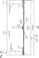
- Fig. 25 shows a typical example of a silicon-based electro-optic phase modulator which uses a rib waveguide shape structure formed on an SOI substrate and is disclosed in each of Patent-related Document 1 and Non-patent-related Document 1.
- the electro-optic phase modulator is formed by applying p-doping and n-doping processes to slab regions extending laterally along both sides of a rib shape comprising an intrinsic semiconductor region.
- the above rib waveguide structure is formed by use of an Si layer on a silicon on insulator (SOI) substrate.
- SOI silicon on insulator
- an intrinsic semiconductor silicon layer 2501 is formed to include a p-type region 2504 which is in contact with a first electrode contacting layer 2506 and is doped at high concentration.
- the intrinsic semiconductor silicon layer 2501 further comprises a region 2505 that is doped at high concentration by applying an n-type doping process, and a second electrode contacting layer 2506 connected to the region 2505.
- the doping process it is possible to apply the doping process to each of the regions 2504 and 2505 in such a manner that the region exhibits carrier density of approximately 10 20 /cm 3 .
- the p-type region 2504 and the n-type region 2505 are positioned at both sides of the rib 2501, respectively, with a distance between the above two regions; and the rib 2501 is an intrinsic semiconductor layer.
- Fig. 25 shows a supporting substrate 2503, a buried oxide film layer 2503, electrode wires 2507, and an oxide cladding 2508.
- an optical conversion operation it is connected to an electric power source in such a manner that a forward bias is applied to the PIN diode by use of the first and second electrode contact layers 2506 to thereby inject free carriers into the waveguide.
- a forward bias is applied to the PIN diode by use of the first and second electrode contact layers 2506 to thereby inject free carriers into the waveguide.
- the refractive index of the silicon layer 2501 changes due to increase of the free carriers; and, as a result, phase modulation of the light, which is transmitted through the waveguide, is induced.
- the speed of the optical modulation operation is restricted by the life of free carriers in the rib 2501 and by carrier diffusion when the forward bias is removed.
- a PIN-diode-type phase modulator such as that of prior art explained above usually operates at a speed around 10-50 Mb/sec when it operates under application of a forward bias.
- NPL 1 William M. J. Green, Michael J. Rooks, Lidija Sekaric, and Yurii A. Vlasof, "Ultra-compact, low RF power, 10Gb/s silicon Mach-Zehnder modulator," Opt. Express 15, 2007,17106-171113
- an optical modulator which has features such that optical loss is small, a size is small, a required voltage is low, and a high-speed operation is possible, is required.
- an optical modulator comprises a rib-type waveguide structure, wherein the rib-type waveguide structure comprises: a PN junction or a PIN junction which comprises Si or Si 1-y Ge y and is formed in a lateral direction on a substrate; and an Si 1-x Ge x layer which comprises at least one layer, is doped by an impurity to exhibit a first conductivity type or a second conductivity type, and is stacked on the PN junction or the PIN junction to be electrically connected to the PN junction or the PIN junction.
- the optical modulator comprises a first electrode of the first conductivity type and a second electrode of the second conductivity type which are positioned adjacent to the rib-type waveguide structure.
- Carrier density of the rib-type waveguide structure changes as a result of voltage supply to the first electrode and the second electrode.
- the Si 1-x Ge x layer comprising at least one layer has a lattice strain.
- the PN junction or the PIN junction formed in the lateral direction on the substrate comprises a layered structure comprising a PN junction or a PIN junction comprising Si and a PN junction or a PIN junction comprising Si 1-y Ge y .
- the PN junction or the PIN junction which comprises the layered structure comprising Si and Si 1-y Ge y and formed in the lateral direction on the substrate, comprises a rib-type waveguide structure.
- the Si 1-x Ge x layer comprising at last one layer comprises an Si 1-x1 Ge x1 layer stacked on the PN junction or the PIN junction, and an Si 1-x2 Ge x2 layer stacked on the Si 1-x1 Ge x1 layer, wherein x2 is smaller than x1.
- the Si 1-x Ge x layer comprising at last one layer comprises a strain induction film formed above the Si 1-x Ge x layer or on a side of the Si 1-x Ge x layer.
- doping concentration of the first conductivity type is lower than doping concentration of the second conductivity type.
- the first conductivity type is a p type
- the second conductivity type is an n type
- the PN junction or the PIN junction comprises a plurality of PN junctions or a plurality of PIN junctions which are formed in a periodic manner or an aperiodic manner along a direction of propagation of light.
- a conductivity type of at least one S 1-x Ge x layer stacked on the PN junction or the PIN junction changes, in an alternating manner, between the first conductivity type and the second conductivity type.
- an optical intensity modulator comprises the above optical phase modulator.
- a method for manufacturing an optical phase modulator comprises: forming a PN junction or a PIN junction which comprises Si or Si 1-y Ge y and is formed in a lateral direction; doping regions adjacent to the PN junction or the PIN junction with a first conductivity type and a second conductivity type to form a first electrode of a first conductivity type and a second electrode of a second conductivity type; and forming, on the PN junction or the PIN junction, an Si 1-x Ge x layer that comprises at least one layer, is doped by an impurity to exhibit the first conductivity type or the second conductivity type, and is electrically connected to the PN junction or the PIN junction.
- the forming the Si 1-x Ge x layer comprising at least one layer comprises forming a concavity in the PN junction or the PIN junction; and forming an Si 1-x Ge x layer comprising at least one layer on the concavity.
- an optical modulator which has features such that optical loss is small, a size is small, a required voltage is low, and a high-speed operation is possible, can be realized.
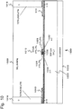
- Fig. 1 schematically shows a cross-section view of an optical phase modulator 100 according to an embodiment of the present invention.
- the optical phase modulator 100 is formed, by use of a silicon photonics technique, on a buried oxide film (BOX) layer 104 comprising silica glass (SiO 2 ) deposited on a silicon (Si) substrate 102.
- the optical phase modulator 100 comprises a rib-type waveguide structure 110.
- the rib-type waveguide structure 110 comprises a PN junction 106 comprising Si and formed in a lateral direction with respect to the substrate (a direction horizontal to the substrate).
- the PN junction 106 comprises a p-type Si region 130 and an n-type Si region 132. As will be explained later, the PN junction 106 may comprise Si 1-y Ge y (y is equal to or greater than 0 and equal to or less than 1).
- the rib-type waveguide structure 110 may comprise a PIN junction in place of the PN junction 106.
- Such a PIN structure may include both a PIN junction that is intentionally formed and a PIN junction that is unintentionally formed as a result of change from a PN junction to a PIN junction. The unintentional case is that an intrinsic region is formed as a result of recombination of electrons and holes due to thermal diffusion in a PN junction 106.
- the rib-type waveguide structure 110 also comprises a S 1-x Ge x layer 108(x is equal to or greater than 0 and equal to or less than 1) that comprises at least one layer that is deposited on the PN junction 106 and has conductivity obtained as a result of introduction of an impurity by doping.
- the conductivity type of the Si 1-x Ge x layer 108 is a p type; however, it is possible to make the conductivity type of the Si 1-x Ge x layer 108 to be an n type. In this manner, the Si 1-x Ge x layer 108 has conductivity; thus, it is electrically connected to the PN junction 106.
- the width of the Si 1-x Ge x layer 108 is 0.4 ⁇ m
- the thickness of the Si 1-x Ge x layer 108 is 20-80 nm
- the distance from the center of the PN junction to the edge of the p-type Si region 130 is 1 ⁇ m.
- the height of the PN junction in the rib-type waveguide structure 110 with respect to a slab layer is 80-100 nm.
- the thickness of each of the electrodes 112 and 114 is 0.10-0.25 ⁇ m.
- the optical phase modulator 100 also comprises a first electrode 112 of a first conductivity type (for example, a p type) and a second electrode 114 of a second conductivity type (for example, an n type) that are positioned adjacent to the rib-type waveguide structure 110, a ground electrode 116 and a signal electrode 118, and a cladding 120.
- the ground electrode 116 and the signal electrode 118 may comprise Ti, TiN, AlSiCu, TiN, or the like, for example.
- the optical phase modulator 100 performs phase modulation of light by using a carrier plasma effect.
- ⁇ n denotes a change in a refractive index
- e denotes a unit charge
- ⁇ denotes a light wavelength
- c denotes the speed of light
- ⁇ 0 denotes a dielectric constant in a vacuum
- n denotes a refractive index of Si
- ⁇ N e denotes a change in electron density
- m* ce denotes an effective mass of an electron
- ⁇ N h denotes a change in hole density
- m* ch denotes an effective mass of a hole.
- the change in the refractive index ⁇ n increases as the effective mass of the electron or the effective mass of the hole decreases.
- ⁇ denotes a change in an optical-absorption coefficient
- ⁇ e denotes electron mobility
- ⁇ h denotes hole mobility
- a strain (lattice strain) is induced in the Si 1-x Ge x layer due to a difference between a lattice constant of the Si layer and a lattice constant of the Si 1-x Ge x layer.
- an effective mass of a carrier becomes smaller.
- the effective mass of the free carrier is reduced by using the Si 1-x Ge x layer 108, compared with the case that a waveguide structure comprising Si only is used.
- the carrier plasma effect can be enhanced, since the change in the refractive index due to the plasma dispersion effect becomes larger.
- a required degree of phase shift can be obtained by use of a distance shorter than that used in a prior-art structure; so that modulation efficiency of the optical phase modulator 100 can be improved, the size of the optical phase modulator 100 can be reduced, and the loss in the optical phase modulator 100 can be reduced. Further, since the effective mass of the free carrier is reduced, the mobility of the free carrier, which is inversely related to the effective mass, increases. Thus, according to this embodiment, a high speed operation of the optical phase modulator 100 can be realized.
- the p-type doping concentration in the PIN junction 106 and/or the Si 1-x Ge x layer 108, it may be possible to set the p-type doping concentration to be lower than the n-type doping concentration.
- An enhancement factor of the carrier plasma effect in the case of SiGe is larger than that in the case of Si.
- an enhancement factor of a hole is approximately two times larger than that of an electron.
- the inventor of the present invention performed simulation, that will be explained later, to verify that an optical phase modulator having a p-type Si 1-x Ge x layer according to an embodiment of the present invention exhibits an improved performance, compared with a prior-art optical phase modulator using Si only.
- Fig. 2 (A) shows a cross-section structure of an optical phase modulator 200 used for simulation.
- the size of each of the parts has a value that is the same as the value exemplified in the above description relating to Fig. 1 .
- the doping concentration in the PN junction 206 is 1x10 18 /m 3 .
- the doping concentration in each of the p-type Si layer 208 and the p-type Si 1-x Ge x layer 208 is 1x10 18 /cm 3 .
- the doping concentration in each of the p-type electrode 212 and the n-type electrode 214 is 1x10 20 /cm 3 .
- a semiconductor device simulator was used for calculating carrier density distribution.
- An optical mode was calculated by use of an electromagnetic field simulator according to a finite element method.
- Fig. 2 (B) shows an optical field (a TE0 mode) calculated with respect to the optical phase modulator 200 shown in Fig. 2 (A) .
- Fig. 3 shows results of calculation of carrier distribution with respect to a case of a structure wherein a p-type Si layer is stacked on a PN junction 206 and a case of a structure wherein a p-type Si 1-x Ge x layer is stacked on the PN junction 206, respectively, when bias voltages are 0 V and -2 V.
- Fig. 3 (A) shows results of calculation in the case that a p-type Si layer is used.
- Fig. 3 (B) shows results of calculation in the case that a p-type Si 1-x Ge x layer is used. In each of the cases shown in Fig.
- a depletion layer becomes wider in the case that a reverse bias of -2 V is applied, compared with the case that the bias voltage is 0 V.
- the depletion layer in the case of Fig. 3 (B) becomes slightly thick, due to band discontinuity at an interface between the p-type Si 1-x Ge x layer and the Si layer forming the PN junction.
- large differences between the results shown in Fig. 3 (A) and (B) could not be observed.
- FIG. 4 (A) and (B) show results of calculation regarding a relationship between a reverse bias voltage and a figure of merit V ⁇ L and a relationship between a reverse bias voltage and an insertion loss, respectively, regarding the optical phase modulator 200 shown in Fig. 2 (A) .
- V ⁇ L is a product of the length and the voltage required for shifting a phase by ⁇ in an optical phase shifter. It is considered that performance of an optical phase modulator becomes higher as V ⁇ L becomes smaller. As would be understood from Fig.
- V ⁇ L becomes smaller by use of the construction wherein a p-type Si 1-x Ge x layer is stacked on the PN junction 206, compared with the case that the construction wherein a p-type Si layer is stacked on the PN junction 206 is used, if bias voltages to be applied to the two constructions are the same.
- the size of the modulator required to obtain a desired change in a refractive index becomes smaller by using a p-type Si 1-x Ge x layer, compared with the case that a Si layer only is used. Accordingly, it becomes possible to reduce the size of the optical phase modulator by using a p-type Si 1-x Ge x layer.
- FIG. 4 (B) show results of calculation regarding a relationship between a bias voltage and an insertion loss per 1 mm.
- the insertion loss becomes larger in the case that a p-type Si 1-x Ge x layer is used, compared with the case that an Si layer is used.
- the size of the optical phase modulator can be reduced by using a p-type Si 1-x Ge x layer, the insertion loss of the optical phase modulator itself does not become substantially large, compared with the case that an Si layer only is used.
- the band gap of Si 1-x Ge x is smaller than that of Si, effect to confine carriers is obtained by stacking a Si 1-x Ge x layer.
- the temperature required for activation annealing for activating a doped impurities is approximately 1000°C in the case of a Si layer; and, on the other hand, the temperature required for activation annealing is approximately 700-800°C in the case of a Si 1-x Ge x layer.
- a doping process is applied to the Si layer constituting the PN junction and an activation annealing process is applied thereto, and, thereafter, a Si layer is stacked and a doping process and an activation annealing process are applied thereto.
- a doping process is applied to the Si layer constituting the PN junction, a p-type doping process is further applied to the upper Si layer, and activation annealing process is applied thereto.
- the latter activation annealing is performed at a temperature of approximately 1000°C; thus, in the case that the impurities doped by the doping process applied to the upper Si layer have reached at the PN junction, thermal diffusion of carriers will occur in the already-formed PN junction.
- the latter activation annealing is performed at a temperature of approximately 700-800°C; thus, even in the case that the impurities doped by the latter doping process have reached at the PN junction, the impurities in the Si 1-x Ge x layer only are activated and the impurities in the Si layer are not activated.
- a very steep and ideal doping interface can be obtained. Accordingly, separation between a calculated value of V ⁇ L and an experimentally-obtained value of V ⁇ L becomes smaller.
- V ⁇ L can be greatly reduced, compared with the case that a Si layer is stacked.
- Difference of the activation annealing temperature after the doping processes also exists in the case that Si 1-x Ge x layers having different compositions are used; so that, even in the case that a p-type Si 1-x Ge x layer having a larger Ge composition is stacked on a PN junction comprising a p-type Si 1-x Ge x layer having a smaller Ge composition, thermal diffusion of carriers can be suppressed and, accordingly, optical modulation efficiency close to a calculated value can be experimentally obtained.
- Fig. 5 (A) shows results of calculation regarding a relationship between an excess loss of light and a distance between an electrode layer (a highly-doped region) and a center part of the rib-type waveguide shape, with respect to the optical phase modulator 200 shown in Fig. 2 (A) .
- a vertical axis of a graph shown in Fig. 5 (A) represents excess loss of light (absorption loss of light due to an electrode), and a horizontal axis of a graph shown in Fig.
- the excess losses are approximately 12 dB/mm and approximately 4 dB/mm when the distances relating to the electrode layer are 0.4 ⁇ m and 0.6 ⁇ m, respectively.
- the excess losses are approximately 2.5 dB/mm and approximately 0 dB/mm when the distances relating to the electrode layer are 0.4 ⁇ m and 0.6 ⁇ m, respectively.
- the electrode layer must be positioned further away for reducing the excess loss.
- the electrode layer can be positioned at a closer place, while suppressing the excess loss.
- the distance relating to the electrode layer constituting a component of the optical phase modulator can be reduced. Accordingly, electrode leading-out resistance between the electrode layer and the optical modulation part comprising the rib-type waveguide shape is reduced, so that a CR time constant of the device can be reduced.
- a high speed operation of the optical phase modulator can be realized.
- Fig. 5 (B) shows results of calculation of optical-electric-field intensity distribution with respect to each of a case wherein a SiGe layer is not used (the top figure in Fig. 5 (B) ) and a case wherein a SiGe layer is used (the bottom figure in Fig. 5 (B) ).
- the refractive index of SiGe is larger than that of Si; so that it can be understood that, by using a SiGe layer, the effect to confine light is enhanced and a mode field becomes smaller.
- the electrode can be positioned at a place closer to the core region of the optical phase modulator. As a result, the resistance in the optical phase modulator can be reduced and the speed of the operation of the optical phase modulator can be increased.
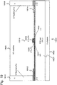
- Fig. 6 schematically shows a cross-section view of an optical phase modulator 600 according to an embodiment of the present invention.
- the structure of the optical phase modulator 600 is similar to that of the optical phase modulator 100 shown in Fig. 1 , except that two p-type SiGe layers (a p-type Si 1-x1 Ge x1 layer 608 and a p-type Si 1-x2 Ge x2 layer 622) are stacked on a PN junction 606 in the optical phase modulator 600. It may be possible to set in such a manner that the ratio of Ge in the p-type Si 1-x2 Ge x2 layer 622 is smaller than that of the p-type Si 1-x1 Ge x1 layer 608 (i.e., x1>x2).
- the p-type Si 1-x1 Ge x1 layer 608 may be a p-type Si 0.7 Ge 0.3 layer
- the p-type Si 1-x2 Ge x2 layer 622 may be a p-type Si 0.8 Ge 0.2 layer.
- the p-type Si 1-x2 Ge x2 layer 622 may be a Si layer. Similar to Fig. 1 , Fig. 6 shows a Si substrate 602, a BOX layer 604, a PN junction 606, a p-type Si region 630, an n-type Si region 632, a first electrode 612, a second electrode 614, a ground electrode 616, a signal electrode 618, and a cladding 620.
- the PN junction 606 may comprise Si 1-y Ge y .
- a rib-type waveguide structure 610 may comprise a PIN junction in place of the PN junction.
- the conductivity type of each of the Si 1-x1 Ge x1 layer 608 and the Si 1-x2 Ge x2 layer 622 may be set to be an n type.
- Fig. 7 schematically shows a cross-section view of an optical phase modulator 700 according to an embodiment of the present invention.
- the structure of the optical phase modulator 700 is similar to that of the optical phase modulator 600 shown in Fig. 6 , except that a strain inducing film 724 is stacked on a p-type Si 1-x2 Ge x2 layer 722 in the optical phase modulator 700.
- large strain is generated by stacking the strain inducing film 724 instead of stacking a thick SiGe layer.
- the strain inducing film 724 may comprise, for example, SiN x or alumina. Similar to Fig. 6 , Fig.
- the PN junction 706 may comprise Si 1-y Ge y .
- a rib-type waveguide structure 710 may comprise a PIN junction in place of the PN junction.
- the conductivity type of each of the Si 1-x1 Ge x1 layer 708 and the Si 1-x2 Ge x2 layer 722 may be set to be an n type.
- Fig. 8 schematically shows a cross-section view of an optical phase modulator 800 according to an embodiment of the present invention.
- the structure of the optical phase modulator 800 is similar to that of the optical phase modulator 600 shown in Fig. 6 , except that strain inducing films 824 are formed in positions adjacent to side surfaces of a p-type Si 1-x2 Ge x2 layer 822 in the optical phase modulator 800.
- the strain inducing films 824 may extend from positions above a PN junction 806 to positions above a first electrode 812 and a second electrode 814.
- the strain inducing films 824 may be formed in positions adjacent to side surfaces of a p-type Si 1-x1 Ge x1 layer 808.
- Fig. 8 shows an Si substrate 802, a BOX layer 804, the PN junction 806, a p-type Si region 830, an n-type Si region 832, the p-type Si 1-x1 Ge x1 layer 808, the first electrode 812, the second electrode 814, a ground electrode 816, a signal electrode 818, and a cladding 820.
- the PN junction 806 may comprise Si 1-y Ge y .
- a rib-type waveguide structure 810 may comprise a PIN junction in place of the PN junction.
- the conductivity type of each of the Si 1-x1 Ge x1 layer 808 and the Si 1-x2 Ge x2 layer 222 may be set to be an n type.
- Fig. 9 schematically shows a cross-section view of an optical phase modulator 900 according to an embodiment of the present invention.
- the structure of the optical phase modulator 900 is similar to that of the optical phase modulator 600 shown in Fig. 6 , except that strain inducing films 924 are formed in positions which are above a p-type Si 1-x2 Ge x2 layer 922 and adjacent to side surfaces of the p-type Si 1-x2 Ge x2 layer 922 in the optical phase modulator 900.
- the strain inducing films 924 are stacked on a p-type Si 1-x2 Ge x2 layer 922, in a manner similar to that of the case of the optical phase modulator 700 shown in Fig. 7 .
- the strain inducing films 924 are formed in positions adjacent to side surfaces of a p-type Si 1-x2 Ge x2 layer 922, in a manner similar to that of the case of the optical phase modulator 800 shown in Fig. 8 .
- the strain inducing films 924 may extend from positions above a PN junction 906 to positions above a first electrode 912 and a second electrode 914.
- the strain inducing films 924 may be formed in positions adjacent to side surfaces of a p-type Si 1-x1 Ge x1 layer 908.
- large strain is generated by forming the strain inducing films 924 instead of stacking a thick SiGe layer.
- the strain inducing films 924 may comprise, for example, SiN x or alumina. Similar to Fig. 6 , Fig. 9 shows a Si substrate 902, a BOX layer 904, the PN junction 906, a p-type Si region 930, an n-type Si region 932, the first electrode 912, the second electrode 914, a ground electrode 916, a signal electrode 918, and a cladding 920.
- the PN junction 906 may comprise Si 1-y Ge y .
- a rib-type waveguide structure 910 may comprise a PIN junction in place of the PN junction.
- the conductivity type of each of the Si 1-x1 Ge x1 layer 908 and the Si 1-x2 Ge x2 layer 922 may be set to be an n type.
- Fig. 10 schematically shows a cross-section view of an optical phase modulator 1000 according to an embodiment of the present invention.
- the structure of the optical phase modulator 1000 is similar to that of the optical phase modulator 100 shown in Fig. 1 , except that a PN junction 1006 comprises a p-type Si 1-y Ge y layer 1026 and an n-type Si 1-y Ge y layer 1028 in the optical phase modulator 1000.
- a PN junction 1006 comprises a p-type Si 1-y Ge y layer 1026 and an n-type Si 1-y Ge y layer 1028 in the optical phase modulator 1000.
- the structures of the layers included in the PN junction 1006 are not limited to the structure described above.
- the value of the ratio of Ge can be set to be any value.
- a p-type Si 1-x1 Ge x1 layer 1008 may comprise two or more p-type Si 1-x Ge x layers (a p-type Si 0.7 Ge 0.3 layer, a p-type Si 0.8 Ge 0.2 layer, etc.). Similar to Fig. 1 , Fig. 10 shows a Si substrate 1002, a BOX layer 1004, a p-type Si region 1030, an n-type Si region 1032, a first electrode 1012, a second electrode 1014, a ground electrode 1016, a signal electrode 1018, and a cladding 1020.
- a rib-type waveguide structure 1010 may comprise a PIN junction in place of the PN junction.
- the conductivity type of the Si 1-x Ge x layer 1008 may be set to be an n type.
- the Ge composition of each of the p-type Si 1-y Ge y layer 1026 and the n-type Si 1-y Ge y layer 1028 may be smaller than the Ge composition of the p-type Si 1-x Ge x layer 1008.
- the Ge composition of each of the p-type Si 1-y Ge y layer 1026 and the n-type Si 1-y Ge y layer 1028 may be 10-20%, and the Ge composition of the p-type Si 1-x Ge x layer 1008 may be 30-50%. Similar to the cases of the optical phase modulators shown in Figs.
- strain inducing films may be formed in positions above the p-type Si 1-x Ge x layer 1008 and/or adjacent to side surfaces of the p-type Si 1-x Ge x layer 1008 in the optical phase modulator 1000 shown in Fig. 10 .
- the PN junction 1006 comprises a layered structure which comprises a PN junction comprising Si and a PN junction comprising Si 1-y Ge y .
- the PN junction 1006 comprises a SiGe layer, the refractive index of the PN junction 1006 becomes higher, compared with that of the optical phase modulator 100 shown in Fig. 1 .
- the effect to confine light is further enhanced, and optical modulation efficiency is improved.
- Fig. 11 schematically shows a cross-section view of an optical phase modulator 1100 according to an embodiment of the present invention.
- the structure of the optical phase modulator 1100 is similar to that of the optical phase modulator 1000 shown in Fig. 10 , except that a p-type Si 1-x2 Ge x2 layer 1122 is stacked on a p-type Si 1-x1 Ge x1 layer 1108 in the optical phase modulator 1100.
- the constructions of the layers included in the PN junction 1106 are not limited to the structures shown in Fig. 11 .
- the value of the ratio of Ge can be set to be any value.
- Fig. 11 shows a Si substrate 1102, a BOX layer 1104, a p-type Si region 1130, an n-type Si region 1132, a first electrode 1112, a second electrode 1114, a ground electrode 1116, a signal electrode 1118, and a cladding 1120.
- a rib-type waveguide structure 1110 may comprise a PIN junction in place of the PN junction.
- the conductivity type of each of the Si 1-x1 Ge x1 layer 1108 and the Si 1-x2 Ge x2 layer 1122 may be set to be an n type. Similar to the cases of the optical phase modulators shown in Figs.
- strain inducing films may be formed in positions above the p-type Si 1-x2 Ge x2 layer 1122 and/or adjacent to side surfaces of the p-type Si 1-x2 Ge x2 layer 1122, and/or above the p-type Si 1-x1 Ge x1 layer 1108 and/or adjacent to side surfaces of the p-type Si 1-x1 Ge x1 layer 1108 in the optical phase modulator 1100 shown in Fig. 11 .
- the PN junction 1106 comprises a SiGe layer, the refractive index of the PN junction 1106 becomes higher, compared with that of a PN junction comprising Si only.
- the effect to confine light is further enhanced, and optical modulation efficiency is improved.
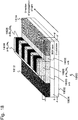
- Fig. 12 schematically shows a perspective view of an optical phase modulator 1200 according to an embodiment of the present invention.
- the optical phase modulator 1200 comprises a Si substrate 1202, a BOX layer 1204, a p-type Si region 1230, an n-type Si region 1232, a p-type Si 1-x Ge x layer 1208, a first electrode 1212, and a second electrode 1214.
- the p-type Si 1-x Ge x layer 1208 is stacked on the p-type Si region 1230 and the n-type Si region 1232.
- the optical phase modulator 1200 is constructed in such a manner that, in the waveguide part, parts of the p-type Si region 1230 and parts of the n-type Si region 1232 are arranged in an alternating manner along the direction of propagation of light.
- a plurality of PN junctions comprising Si are formed along the direction of propagation of light.
- parts of the p-type Si region 1230 and parts of the n-type Si region 1232 arranged in an alternating manner are drawn in such a manner that the widths thereof (the widths along the direction of propagation of light) are approximately equal to each other; thus, it is understood that a plurality of PN junctions are formed in a periodic manner along the direction of propagation of light.
- the PN junction may be replaced by a PIN junction.
- the widths of parts of the p-type Si region 1230 and parts of the n-type Si region 1232 arranged in an alternating manner may be different from each other.
- a plurality of PN junctions or PIN junctions may be formed in an aperiodic manner along the direction of propagation of light.
- FIG. 13 corresponds to a cross-section view at line A-A' in Fig. 12
- Fig. 14 corresponds to a cross-section view at line B-B' in Fig. 12
- the p-type Si region 1230 extends up to the right edge of the p-type Si 1-x Ge x layer 1208.
- the n-type Si region 1232 extends up to the left edge of the p-type Si 1-x Ge x layer 1208.
- each of Figs. 13 and 14 shows the Si substrate 1202, the BOX layer 1204, the p-type Si 1-x Ge x layer 1208, a rib-type waveguide structure 1210, the first electrode 1212, the second electrode 1214, a ground electrode 1216, a signal electrode 1218, and a cladding 1220.
- the conductivity type of the Si 1-x Ge x layer 1208 may be set to be an n type.
- Fig. 15 schematically shows a perspective view of an optical phase modulator 1500 according to an embodiment of the present invention. Similar to the optical phase modulator 1200 shown in Fig. 12 , the optical phase modulator 1500 comprises an Si substrate 1502, a BOX layer 1504, a p-type Si region 1530, an n-type Si region 1532, a first electrode 1512, and a second electrode 1514.
- the optical phase modulator 1500 is constructed in such a manner that, in the waveguide part, parts of the p-type Si region 1530 and parts of the n-type Si region 1532 are arranged in an alternating manner along the direction of propagation of light. Thus, a plurality of PN junctions are formed in a periodic manner along the direction of propagation of light.
- the conductivity type of at least one Si 1-x Ge x layer stacked on the PN junctions in the optical phase modulator 1500 changes, in an alternating manner, between a first conductivity type (for example, a p type) and a second conductivity type (for example, an n type). That is, in the optical waveguide part, a p-type Si 1-x Ge x layer 1508 is formed on a part of the p-type Si region 1530, and an n-type Si 1-x Ge x layer 1534 is formed on a part of the n-type Si region 1532.
- a first conductivity type for example, a p type
- a second conductivity type for example, an n type
- the PN junction may be replaced by a PIN junction.
- the widths of parts of the p-type Si region 1530 and parts of the n-type Si region 1532 arranged in an alternating manner may be different from each other.
- a plurality of PN junctions or PIN junctions may be formed in an aperiodic manner along the direction of propagation of light.
- the conductivity type of at least one Si 1-x Ge x layer stacked on a plurality of PN junctions or a plurality of PIN junctions may change between a first conductivity type and a second conductivity type, in an alternating manner.
- FIG. 16 corresponds to a cross-section view at line A-A' in Fig. 15
- Fig. 17 corresponds to a cross-section view at line B-B' in Fig. 15
- the p-type Si 1-x Ge x layer 1508 is formed in Fig. 16 .
- the p-type Si region 1530 extends up to the right edge of the p-type Si 1-x Ge x layer 1508.
- the n-type Si 1-x Ge x layer 1534 is formed in Fig. 17 .
- the n-type Si region 1532 extends up to the left edge of the n-type Si 1-x Ge x layer 1534. Further, each of Figs. 16 and 17 shows the Si substrate 1502, the BOX layer 1504, a rib-type waveguide structure 1510, the first electrode 1512, the second electrode 1514, a ground electrode 1516, a signal electrode 1518, and a cladding 1520.
- Fig. 18 schematically shows a perspective view of an optical phase modulator 1800 according to an embodiment of the present invention.
- the optical phase modulator 1800 comprises a Si substrate 1802, a BOX layer 1804, a p-type Si region 1830, an n-type Si region 1832, p-type Si 1-y Ge y layers 1826, n-type Si 1-y Ge y layers 1828, a p-type Si 1-x Ge x layer 1808, a first electrode 1812, and a second electrode 1814.
- the p-type Si 1-x Ge x layer 1808 is stacked on the p-type Si 1-y Ge y layers 1826 and the n-type Si 1-y Ge y layers 1828.
- the optical phase modulator 1800 is constructed in such a manner that, in the waveguide part, "parts of the p-type Si region 1830 and the p-type Si 1-y Ge y layers 1826" and "parts of the n-type Si region 1832 and the n-type Si 1-y Ge y layers 1828" are arranged in an alternating manner along the direction of propagation of light. Thus, a plurality of PN junctions comprising Si and SiGe are formed along the direction of propagation of light. In Fig.
- the widths of "the parts of the p-type Si region 1830 and the p-type Si 1-y Ge y layers 1826" and “the parts of the n-type Si region 1832 and the n-type Si 1-y Ge y layers 1828" arranged in an alternative manner are approximately equal to each other, and, thus, a plurality of PN junctions are formed in a periodic manner along the direction of propagation of light.
- the PN junction may be replaced by a PIN junction.
- the widths of "the parts of the p-type Si region 1830 and the p-type Si 1-y Ge y layers 1826" and “the parts of the n-type Si region 1832 and the n-type Si 1-y Ge y layers 1828" arranged in an alternating manner may be different from each other.
- a plurality of PN junctions or PIN junctions may be formed in an aperiodic manner along the direction of propagation of light.
- FIG. 19 schematically shows a cross-section view of the optical phase modulator 1800 shown in Fig. 18 .
- Fig. 19 corresponds to a cross-section view at line A-A' in Fig. 18
- Fig. 20 corresponds to a cross-section view at line B-B' in Fig. 18 .
- the p-type Si region 1830 extends up to the right edge of the p-type S 1-x Ge x layer 1808, and the p-type Si 1-y Ge y layer 1826 is stacked on the p-type Si region 1830.
- Fig. 19 it is shown in Fig. 19 that the p-type Si region 1830 extends up to the right edge of the p-type S 1-x Ge x layer 1808, and the p-type Si 1-y Ge y layer 1826 is stacked on the p-type Si region 1830.
- Fig. 19 it is shown in Fig. 19 that the p-type Si region 1830 extends up to the right edge of the
- n-type Si region 1832 extends up to the left edge of the p-type Si 1-x Ge x layer 1808, and the n-type Si 1-y Ge y layer 1828 is stacked on the n-type Si region 1832.
- each of Figs. 19 and 20 shows the Si substrate 1802, the BOX layer 1804, a rib-type waveguide structure 1810, the first electrode 1812, the second electrode 1814, a ground electrode 1816, a signal electrode 1818, and a cladding 1820.
- the conductivity type of the Si 1-x Ge x layer 1808 may be set to be an n type.
- Fig. 21 schematically shows a perspective view of an optical phase modulator 2100 according to an embodiment of the present invention. Similar to the optical phase modulator 1800 shown in Fig. 18 , the optical phase modulator 2100 comprises an Si substrate 2102, a BOX layer 2104, a p-type Si region 2130, an n-type Si region 2132, p-type Si 1-y Ge y layers 2126, n-type Si 1-y Ge y layers 2128, a first electrode 2112, and a second electrode 2114.
- the optical phase modulator 2100 is constructed in such a manner that, in the waveguide part, "parts of the p-type Si region 2130 and the p-type Si 1-y Ge y layers 2126" and "parts of the n-type Si region 2132 and the n-type Si 1-y Ge y layers 2128" are arranged in an alternating manner along the direction of propagation of light.
- a plurality of PN junctions comprising Si and SiGe are formed along the direction of propagation of light.
- SiGe layers are stacked on the plurality of PN junctions.
- the conductivity type of at least one Si 1-x Ge x layer stacked on the PN junctions in the optical phase modulator 2100 changes, in an alternating manner, between a first conductivity type (for example, a p type) and a second conductivity type (for example, an n type). That is, in the optical waveguide part, a p-type Si 1-x Ge x layer 2108 is formed on the p-type Si 1-y Ge y layer 2126, and an n-type Si 1-x Ge x layer 2134 is formed on the n-type Si 1-y Ge y layer 2128.
- a first conductivity type for example, a p type
- a second conductivity type for example, an n type
- the PN junction may be replaced by a PIN junction.
- the widths of "the parts of the p-type Si region 2130 and the p-type Si 1-y Ge y layers 2126" and “the parts of the n-type Si region 2132 and the n-type Si 1-y Ge y layers 2128" arranged in an alternating manner may be different from each other.
- a plurality of PN junctions or PIN junctions may be formed in an aperiodic manner along the direction of propagation of light.
- the conductivity type of at least one Si 1-x Ge x layer stacked on plurality of PN junctions or plurality of PIN junctions may change between a first conductivity type and a second conductivity type, in an alternating manner.
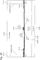
- FIG. 22 schematically shows a cross-section view of the optical phase modulator 2100 shown in Fig. 21 .
- Fig. 22 corresponds to a cross-section view at line A-A' in Fig. 21
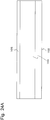
- Fig. 23 corresponds to a cross-section view at line B-B' in Fig. 21 ;
- the p-type Si 1-y Ge y layers 2126 and the p-type Si 1-x Ge x layer 2108 are formed.
- the p-type Si region 2130 extends up to the right edge of the p-type Si 1-x Ge x layer 2108.
- n-type Si 1-y Ge y layer 2128 and the n-type Si 1-x Ge x layer 2134 are formed in Fig. 23 .
- the n-type Si region 2132 extends up to the left edge of the n-type Si 1-x Ge x layer 2134.
- each of Figs. 22 and 23 shows the Si substrate 2102, the BOX layer 2104, a rib-type waveguide structure 2110, the first electrode 2112, the second electrode 2114, a ground electrode 2116, a signal electrode 2118, and a cladding 2120.
- An embodiment of the present invention is an optical intensity modulator comprising an optical phase modulator according to an embodiment of the present invention such as that explained above.
- an optical intensity modulator can be constructed by using, for example, the optical phase modulator 100 shown in Fig. 1 in one arm or both arms of a Mach-Zehnder interferometer.
- An optical phase modulator according to another embodiment of the present invention may also be used for constructing an optical intensity modulator.
- a construction of an optical intensity modulator according to an embodiment of the present invention is not limited to the above-described construction. It will be understood that an optical intensity modulator having a characteristic of the present invention can be constructed by applying, by use of a method known to a person skilled in the art, an optical phase modulator according to the present invention to an optical intensity modulator.
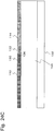
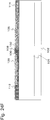
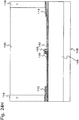
- Figs. 24A to 24H are figures for explaining processes for manufacturing the optical phase modulator 100 according to the embodiment of the present invention shown in Fig. 1 .
- Fig. 24A shows a construction of the substrate used in the embodiment of the present invention. It comprises an SOI substrate wherein the Si layer 105 is stacked on the BOX layer (a thermal oxide film) 104 which is stacked on the Si substrate 102.
- the Si layer 105 is stacked on the BOX layer (a thermal oxide film) 104 which is stacked on the Si substrate 102.
- the p-type Si region 130 is formed by applying a doping process (in which boron is used, for example) to a part of the Si layer 105.
- the n-type Si region 132 is formed by applying a doping process (in which phosphorus is used, for example) to a different part of the Si layer 105.
- the PN junction 106 which comprises Si and is formed in a lateral direction on the substrate, is formed.
- the PN junction may comprise Si 1-y Ge y layer.
- a PIN junction may be formed instead of the PN junction.
- the p-type electrode 112 is formed by further applying a p-type doping process to a part of the p-type Si region 130 that is adjacent to the PN junction 106, to thereby increase doping concentration of the part.
- the n-type electrode 114 is formed by further applying an n-type doping process to a part of the n-type Si region 132 that is adjacent to the PN junction 106, to thereby increase doping concentration of the part.
- Fig. 24D parts of the PN junction 106, the p-type electrode 112, and the n-type electrode 114 are etched.
- an oxide-film mask layer 136 is formed on the etched parts. Further, a part of the oxide-film mask layer, which is on the PN junction 106, is removed, and a concavity 138 is formed.
- a Si 1-x Ge x layer comprising at least one layer is formed on the concavity 138, and the p-type Si 1-x Ge x layer 108 is formed by applying a p-type doping to the above Si 1-x Ge x layer.
- the p-type Si 1-x Ge x layer 108 is electrically connected to the PN junction 106.
- the oxide-film mask layer 136 is removed, and the oxide-film (for example, SiO 2 ) cladding layer 120 is formed.
- the ground electrode 116 and the signal electrode 118 are formed by use of metal wires in such a manner that they contact the p-type electrode 112 and the n-type electrode 114, respectively.
Landscapes
- Physics & Mathematics (AREA)
- Nonlinear Science (AREA)
- General Physics & Mathematics (AREA)
- Optics & Photonics (AREA)
- Optical Modulation, Optical Deflection, Nonlinear Optics, Optical Demodulation, Optical Logic Elements (AREA)
Abstract
Description
- The present invention relates to optical modulators and methods for manufacturing the optical modulators, and more specifically, relates to optical phase modulators and optical intensity modulators that utilize a carrier plasma effect of silicon (Si), and methods for manufacturing these modulators.
- Silicon-based optical communication devices, which function by use of optical fiber communication wavelengths of 1310 nm and 1550 nm that are used in a variety of systems such as a home-use optical fiber, a local area network (LAN), and so on, have great potential in terms of techniques that allow integration of optical function elements and electronic circuits on a silicon platform by use of a CMOS technique.
- Recently, passive devices, such as a waveguide, an optical coupler, a wavelength filter, and so on which are silicon based, are studied very widely. Further, active elements, such as an optical modulator, an optical switch, and so on which are silicon based, can be listed as those that are important in the techniques used in the means for controlling optical signals used in the above communication systems; and these active elements are receiving great attention. The operation of each of an optical switch and a modulation element, which changes a refractive index by use of a thermooptic effect of silicon, is slow; thus, it can support a modulation frequency of up to 1 Mb/sec only, in terms of a device speed. Accordingly, an optical modulation element which uses an electro-optic effect is necessary, for realizing a high modulation frequency that is required in many optical communication systems.
- Many of the presently suggested electro-optic modulators are devices, each of which uses a carrier plasma effect for changing density of free carriers in a silicon layer to thereby change a real part and an imaginary part of a refractive index, for changing the phase and/or the intensity of light. Pure silicon does not exhibit a linear electro-optic effect (Pockels), and change in a refractive index due to a Franz-Keldysh effect or a Kerr effect is very small; thus, the above effect is widely used. In a modulator which uses free carrier absorption, the output thereof is directly modulated in accordance with change in the degree of absorption of light propagating through Si. As a structure using change in a refractive index, a structure using a Mach-Zehnder interferometer is generally known, wherein it is possible to obtain an intensity modulation signal of light by causing interference relating to an optical phase difference between two arms to be occurred.
- Free-carrier density in an electro-optic modulator can be changed by injecting, accumulating, excluding, or inverting free carriers. Many of those devices, that have been studied, have bad optical modulation efficiency, require the length on the order of millimeters for optical phase modulation, and require injection current density higher than 1 kA/cm3. For realizing miniaturization/high-integration, and for further realizing low electric power consumption, an element structure that has high optical modulation efficiency is required; and, by using the element structure, the length for optical phase modulation can be reduced. Also, in the case that the size of an element is large, the element is susceptible to temperature distribution on a silicon platform; so that there may be a case that an originally existed electro-optic effect may be cancelled out by the change in a refractive index of a silicon layer due to a thermooptic effect; and this may become a problem.
-
Fig. 25 shows a typical example of a silicon-based electro-optic phase modulator which uses a rib waveguide shape structure formed on an SOI substrate and is disclosed in each of Patent-related Document 1 and Non-patent-related Document 1. The electro-optic phase modulator is formed by applying p-doping and n-doping processes to slab regions extending laterally along both sides of a rib shape comprising an intrinsic semiconductor region. The above rib waveguide structure is formed by use of an Si layer on a silicon on insulator (SOI) substrate. The structure shown inFig. 25 corresponds to a PIN-diode-type modulator which has a structure such that free carrier density in the intrinsic semiconductor region is changed by applying a forward bias and a reverse bias, for using a carrier plasma effect to thereby change the refractive index. In this example, an intrinsicsemiconductor silicon layer 2501 is formed to include a p-type region 2504 which is in contact with a firstelectrode contacting layer 2506 and is doped at high concentration. In the figure, the intrinsicsemiconductor silicon layer 2501 further comprises aregion 2505 that is doped at high concentration by applying an n-type doping process, and a secondelectrode contacting layer 2506 connected to theregion 2505. In the above PIN diode structure, it is possible to apply the doping process to each of theregions type region 2504 and the n-type region 2505 are positioned at both sides of therib 2501, respectively, with a distance between the above two regions; and therib 2501 is an intrinsic semiconductor layer. Further,Fig. 25 shows a supportingsubstrate 2503, a buriedoxide film layer 2503,electrode wires 2507, and an oxide cladding 2508. - Regarding an optical conversion operation, it is connected to an electric power source in such a manner that a forward bias is applied to the PIN diode by use of the first and second
electrode contact layers 2506 to thereby inject free carriers into the waveguide. At that time, the refractive index of thesilicon layer 2501 changes due to increase of the free carriers; and, as a result, phase modulation of the light, which is transmitted through the waveguide, is induced. In this regard, the speed of the optical modulation operation is restricted by the life of free carriers in therib 2501 and by carrier diffusion when the forward bias is removed. A PIN-diode-type phase modulator such as that of prior art explained above usually operates at a speed around 10-50 Mb/sec when it operates under application of a forward bias. On the other hand, although it is possible to increase an operating speed by introducing an impurity into a silicon layer for shortening the life time of the carriers, there is a problem that efficiency of the optical modulation is lowered by the introduced impurity. However, the most important factor that has effect on the operation speed relates to an RC time constant; and, in this case, the electrostatic capacity (C) at the time that the forward bias is applied becomes very large, as a result of large carrier life time of carriers in the PIN junction. Theoretically, it is possible to realize a high speed operation for the PN junction by applying a reverse bias; however, a relatively high driving voltage or an element having a relatively large size is required to obtain enough optical modulation amplitude. - PTL 1: JP Patent Application Public Disclosure No.
2013-214044 - NPL 1: William M. J. Green, Michael J. Rooks, Lidija Sekaric, and Yurii A. Vlasof, "Ultra-compact, low RF power, 10Gb/s silicon Mach-Zehnder modulator," Opt. Express 15, 2007,17106-171113
- Thus, an optical modulator, which has features such that optical loss is small, a size is small, a required voltage is low, and a high-speed operation is possible, is required.
- In an embodiment of the present invention, an optical modulator comprises a rib-type waveguide structure, wherein the rib-type waveguide structure comprises: a PN junction or a PIN junction which comprises Si or Si1-yGey and is formed in a lateral direction on a substrate; and an Si1-xGex layer which comprises at least one layer, is doped by an impurity to exhibit a first conductivity type or a second conductivity type, and is stacked on the PN junction or the PIN junction to be electrically connected to the PN junction or the PIN junction.
- In an embodiment of the present invention, the optical modulator comprises a first electrode of the first conductivity type and a second electrode of the second conductivity type which are positioned adjacent to the rib-type waveguide structure. Carrier density of the rib-type waveguide structure changes as a result of voltage supply to the first electrode and the second electrode.
- In an embodiment of the present invention, the Si1-xGex layer comprising at least one layer has a lattice strain.
- In an embodiment of the present invention, the PN junction or the PIN junction formed in the lateral direction on the substrate comprises a layered structure comprising a PN junction or a PIN junction comprising Si and a PN junction or a PIN junction comprising Si1-yGey.
- In an embodiment of the present invention, the PN junction or the PIN junction, which comprises the layered structure comprising Si and Si1-yGey and formed in the lateral direction on the substrate, comprises a rib-type waveguide structure.
- In an embodiment of the present invention, the Si1-xGex layer comprising at last one layer comprises an Si1-x1Gex1 layer stacked on the PN junction or the PIN junction, and an Si1-x2Gex2 layer stacked on the Si1-x1Gex1 layer, wherein x2 is smaller than x1.
- In an embodiment of the present invention, the Si1-xGex layer comprising at last one layer comprises a strain induction film formed above the Si1-xGex layer or on a side of the Si1-xGex layer.
- In an embodiment of the present invention, in the PN junction or the PIN junction formed in the lateral direction on the substrate, or in the Si1-xGex layer comprising at last one layer and stacked on the PN junction or the PIN junction to be electrically connected to the PN junction or the PIN junction, doping concentration of the first conductivity type is lower than doping concentration of the second conductivity type.
- In an embodiment of the present invention, the first conductivity type is a p type, and the second conductivity type is an n type.
- In an embodiment of the present invention, the PN junction or the PIN junction comprises a plurality of PN junctions or a plurality of PIN junctions which are formed in a periodic manner or an aperiodic manner along a direction of propagation of light.
- In an embodiment of the present invention, corresponding to junction positions of the plurality of PN junctions or the plurality of PIN junctions which are formed in a periodic manner or an aperiodic manner, a conductivity type of at least one S1-xGex layer stacked on the PN junction or the PIN junction changes, in an alternating manner, between the first conductivity type and the second conductivity type.
- In an embodiment of the present invention, an optical intensity modulator comprises the above optical phase modulator.
- In an embodiment of the present invention, a method for manufacturing an optical phase modulator comprises: forming a PN junction or a PIN junction which comprises Si or Si1-yGey and is formed in a lateral direction; doping regions adjacent to the PN junction or the PIN junction with a first conductivity type and a second conductivity type to form a first electrode of a first conductivity type and a second electrode of a second conductivity type; and forming, on the PN junction or the PIN junction, an Si1-xGex layer that comprises at least one layer, is doped by an impurity to exhibit the first conductivity type or the second conductivity type, and is electrically connected to the PN junction or the PIN junction.
- In an embodiment of the present invention, the forming the Si1-xGex layer comprising at least one layer comprises forming a concavity in the PN junction or the PIN junction; and forming an Si1-xGex layer comprising at least one layer on the concavity.
- According to the present invention, an optical modulator, which has features such that optical loss is small, a size is small, a required voltage is low, and a high-speed operation is possible, can be realized.
-
-
Fig. 1 schematically shows a cross-section view of anoptical phase modulator 100 according to an embodiment of the present invention. -
Fig. 2 (A) shows a cross-section structure of an optical phase modulator used for simulation.Fig. 2 (B) shows an optical field calculated with respect to the optical phase modulator shown inFig. 2 (A) . -
Fig. 3 shows results of calculation of carrier distribution with respect to a case of a structure wherein a p-type Si layer is stacked on a PN junction and a case of a structure wherein a p-type S1-xGex layer is stacked on the PN junction, respectively, when bias voltages are 0 V and -2 V. -
Fig. 4 shows results of calculation regarding a relationship between a reverse bias voltage and a figure of merit V π L and a relationship between a reverse bias voltage and an insertion loss regarding the optical phase modulator shown inFig. 2 (A) . -
Fig. 5 (A) shows results of calculation regarding a relationship between an excess loss of light and a distance between electrodes (highly-doped regions) regarding the optical phase modulator shown inFig. 2 (A) .Fig. 5 (B) shows results of calculation of optical-electric-field profiles with respect to a case that a SiGe layer is not used and a case that an SiGe layer is used, respectively. -
Fig. 6 schematically shows a cross-section view of anoptical phase modulator 600 according to an embodiment of the present invention. -
Fig. 7 schematically shows a cross-section view of anoptical phase modulator 700 according to an embodiment of the present invention. -
Fig. 8 schematically shows a cross-section view of anoptical phase modulator 800 according to an embodiment of the present invention. -
Fig. 9 schematically shows a cross-section view of anoptical phase modulator 900 according to an embodiment of the present invention. -
Fig. 10 schematically shows a cross-section view of an optical phase modulator 1000 according to an embodiment of the present invention. -
Fig. 11 schematically shows a cross-section view of anoptical phase modulator 1100 according to an embodiment of the present invention. -
Fig. 12 schematically shows a perspective view of anoptical phase modulator 1200 according to an embodiment of the present invention. -
Fig. 13 schematically shows a cross-section view of the optical phase modulator shown inFig. 12 . -
Fig. 14 schematically shows a cross-section view of the optical phase modulator shown inFig. 12 . -
Fig. 15 schematically shows a perspective view of anoptical phase modulator 1500 according to an embodiment of the present invention. -
Fig. 16 schematically shows a cross-section view of the optical phase modulator shown inFig. 15 . -
Fig. 17 schematically shows a cross-section view of the optical phase modulator shown inFig. 15 . -
Fig. 18 schematically shows a perspective view of anoptical phase modulator 1800 according to an embodiment of the present invention. -
Fig. 19 schematically shows a cross-section view of the optical phase modulator shown inFig. 18 . -
Fig. 20 schematically shows a cross-section view of the optical phase modulator shown inFig. 18 . -
Fig. 21 schematically shows a perspective view of anoptical phase modulator 2100 according to an embodiment of the present invention. -
Fig. 22 schematically shows a cross-section view of the optical phase modulator shown inFig. 21 . -
Fig. 23 schematically shows a cross-section view of the optical phase modulator shown inFig. 21 . -
Fig. 24A is a figure for explaining a process for manufacturing the optical phase modulator according to the embodiment of the present invention shown inFig. 1 . -
Fig. 24B is a figure for explaining a process for manufacturing the optical phase modulator according to the embodiment of the present invention shown inFig. 1 . -
Fig. 24C is a figure for explaining a process for manufacturing the optical phase modulator according to the embodiment of the present invention shown inFig. 1 . -
Fig. 24D is a figure for explaining a process for manufacturing the optical phase modulator according to the embodiment of the present invention shown inFig. 1 . -
Fig. 24E is a figure for explaining a process for manufacturing the optical phase modulator according to the embodiment of the present invention shown inFig. 1 . -
Fig. 24F is a figure for explaining a process for manufacturing the optical phase modulator according to the embodiment of the present invention shown inFig. 1 . -
Fig. 24G is a figure for explaining a process for manufacturing the optical phase modulator according to the embodiment of the present invention shown inFig. 1 . -
Fig. 24H is a figure for explaining a process for manufacturing the optical phase modulator according to the embodiment of the present invention shown inFig. 1 . -
Fig. 25 shows a typical example of a prior-art silicon-based electro-optic phase modulator. - Embodiments of the present invention will be explained in the following paragraphs with reference to the figures.
Fig. 1 schematically shows a cross-section view of anoptical phase modulator 100 according to an embodiment of the present invention. In this embodiment, theoptical phase modulator 100 is formed, by use of a silicon photonics technique, on a buried oxide film (BOX)layer 104 comprising silica glass (SiO2) deposited on a silicon (Si)substrate 102. Theoptical phase modulator 100 comprises a rib-type waveguide structure 110. The rib-type waveguide structure 110 comprises aPN junction 106 comprising Si and formed in a lateral direction with respect to the substrate (a direction horizontal to the substrate). ThePN junction 106 comprises a p-type Si region 130 and an n-type Si region 132. As will be explained later, thePN junction 106 may comprise Si1-yGey (y is equal to or greater than 0 and equal to or less than 1). The rib-type waveguide structure 110 may comprise a PIN junction in place of thePN junction 106. Such a PIN structure may include both a PIN junction that is intentionally formed and a PIN junction that is unintentionally formed as a result of change from a PN junction to a PIN junction. The unintentional case is that an intrinsic region is formed as a result of recombination of electrons and holes due to thermal diffusion in aPN junction 106. The rib-type waveguide structure 110 also comprises a S1-xGex layer 108(x is equal to or greater than 0 and equal to or less than 1) that comprises at least one layer that is deposited on thePN junction 106 and has conductivity obtained as a result of introduction of an impurity by doping. In this embodiment, the conductivity type of the Si1-xGex layer 108 is a p type; however, it is possible to make the conductivity type of the Si1-xGex layer 108 to be an n type. In this manner, the Si1-xGex layer 108 has conductivity; thus, it is electrically connected to thePN junction 106. - As shown in
Fig. 1 , as examples, the width of the Si1-xGex layer 108 is 0.4 µm, the thickness of the Si1-xGex layer 108 is 20-80 nm, and the distance from the center of the PN junction to the edge of the p-type Si region 130 is 1 µm. Further, as shown inFig. 1 , as an example, the height of the PN junction in the rib-type waveguide structure 110 with respect to a slab layer is 80-100 nm. Still further, as shown inFig. 1 as examples, the thickness of each of theelectrodes - The
optical phase modulator 100 also comprises afirst electrode 112 of a first conductivity type (for example, a p type) and asecond electrode 114 of a second conductivity type (for example, an n type) that are positioned adjacent to the rib-type waveguide structure 110, aground electrode 116 and asignal electrode 118, and acladding 120. Theground electrode 116 and thesignal electrode 118 may comprise Ti, TiN, AlSiCu, TiN, or the like, for example. By applying a voltage to thefirst electrode 112 and thesecond electrode 114 via theground electrode 116 and thesignal electrode 118, the carrier density in the rib-type waveguide structure 110 changes. - The
optical phase modulator 100 performs phase modulation of light by using a carrier plasma effect. Change of a refractive index due to a plasma dispersion effect in the carrier plasma effect can be represented by the following formula.
[Formula 1]
- In the above formula, Δn denotes a change in a refractive index, e denotes a unit charge, λ denotes a light wavelength, c denotes the speed of light, ε0 denotes a dielectric constant in a vacuum, n denotes a refractive index of Si, ΔNe denotes a change in electron density, m*ce denotes an effective mass of an electron, ΔNh denotes a change in hole density, and m*ch denotes an effective mass of a hole. As would be understood from formula (1), the change in the refractive index Δn increases as the effective mass of the electron or the effective mass of the hole decreases.
- Change in an optical-absorption coefficient due to free carrier absorption in the carrier plasma effect can be represented by the following formula.
[Formula 2]
- In the above formula, Δα denotes a change in an optical-absorption coefficient, µe denotes electron mobility, and µh denotes hole mobility. As would be understood from formula (2), the change in the optical-absorption coefficient Δα increases as the effective mass of the electron or the effective mass of the hole decreases.
- By stacking the Si1-xGex layer on the Si layer, a strain (lattice strain) is induced in the Si1-xGex layer due to a difference between a lattice constant of the Si layer and a lattice constant of the Si1-xGex layer. In the case that a strain is induced in the Si1-xGex layer, an effective mass of a carrier becomes smaller. Thus, the effective mass of the free carrier is reduced by using the Si1-xGex layer 108, compared with the case that a waveguide structure comprising Si only is used. Thus, as would be understood from formula (1), the carrier plasma effect can be enhanced, since the change in the refractive index due to the plasma dispersion effect becomes larger. Thus, according to this embodiment, a required degree of phase shift can be obtained by use of a distance shorter than that used in a prior-art structure; so that modulation efficiency of the
optical phase modulator 100 can be improved, the size of theoptical phase modulator 100 can be reduced, and the loss in theoptical phase modulator 100 can be reduced. Further, since the effective mass of the free carrier is reduced, the mobility of the free carrier, which is inversely related to the effective mass, increases. Thus, according to this embodiment, a high speed operation of theoptical phase modulator 100 can be realized. - Also, in the
PIN junction 106 and/or the Si1-xGex layer 108, it may be possible to set the p-type doping concentration to be lower than the n-type doping concentration. An enhancement factor of the carrier plasma effect in the case of SiGe is larger than that in the case of Si. Especially, an enhancement factor of a hole is approximately two times larger than that of an electron. Thus, by making the doping concentration of the p-type SiGe layer to be lower than that of the n-type SiGe layer, the trade-off relationship between the refractive-index difference and the absorption coefficient can be alleviated. As a result, increase of the optical-absorption coefficient can be suppressed and, therefore, a high speed operation can be realized. - The inventor of the present invention performed simulation, that will be explained later, to verify that an optical phase modulator having a p-type Si1-xGex layer according to an embodiment of the present invention exhibits an improved performance, compared with a prior-art optical phase modulator using Si only.
-
Fig. 2 (A) shows a cross-section structure of an optical phase modulator 200 used for simulation. The optical phase modulator 200 comprises: aBOX layer 204 having a thickness of 1-3 µm; awaveguide structure 210 comprising aPN junction 206 that comprises Si and is formed on theBOX layer 204, and a p-type Si layer 208 or a p-type Si1-xGex layer 208 (x=0.3) stacked on thePN junction 206; and a p-type electrode 212 and an n-type electrode 214 that are positioned adjacent to thewaveguide structure 210. The size of each of the parts has a value that is the same as the value exemplified in the above description relating toFig. 1 . The doping concentration in thePN junction 206 is 1x10¹⁸/m3. The doping concentration in each of the p-type Si layer 208 and the p-type Si1-xGex layer 208 is 1x10¹⁸/cm3. The doping concentration in each of the p-type electrode 212 and the n-type electrode 214 is 1x10²⁰/cm3. A semiconductor device simulator was used for calculating carrier density distribution. An optical mode was calculated by use of an electromagnetic field simulator according to a finite element method.Fig. 2 (B) shows an optical field (a TE0 mode) calculated with respect to the optical phase modulator 200 shown inFig. 2 (A) . -
Fig. 3 shows results of calculation of carrier distribution with respect to a case of a structure wherein a p-type Si layer is stacked on aPN junction 206 and a case of a structure wherein a p-type Si1-xGex layer is stacked on thePN junction 206, respectively, when bias voltages are 0 V and -2 V.Fig. 3 (A) shows results of calculation in the case that a p-type Si layer is used.Fig. 3 (B) shows results of calculation in the case that a p-type Si1-xGex layer is used. In each of the cases shown inFig. 3 (A) and (B) , a depletion layer becomes wider in the case that a reverse bias of -2 V is applied, compared with the case that the bias voltage is 0 V. According to the results shown inFig. 3 , the depletion layer in the case ofFig. 3 (B) becomes slightly thick, due to band discontinuity at an interface between the p-type Si1-xGex layer and the Si layer forming the PN junction. However, large differences between the results shown inFig. 3 (A) and (B) could not be observed. - On the other hand, as described above, the carrier plasma effect is affected by the effective mass of the carrier.
Fig. 4 (A) and (B) show results of calculation regarding a relationship between a reverse bias voltage and a figure of merit VπL and a relationship between a reverse bias voltage and an insertion loss, respectively, regarding the optical phase modulator 200 shown inFig. 2 (A) . VπL is a product of the length and the voltage required for shifting a phase by π in an optical phase shifter. It is considered that performance of an optical phase modulator becomes higher as VπL becomes smaller. As would be understood fromFig. 4 (A) , VπL becomes smaller by use of the construction wherein a p-type Si1-xGex layer is stacked on thePN junction 206, compared with the case that the construction wherein a p-type Si layer is stacked on thePN junction 206 is used, if bias voltages to be applied to the two constructions are the same. For example, as shown inFig. 4 (A) , in the case that the bias voltage is -2 V, VπL=0.9 Vcm in the construction using a p-type Si layer; and, on the other hand, VπL=0.67 Vcm in the construction using a p-type Si1-xGex layer. Thus, the size of the modulator required to obtain a desired change in a refractive index becomes smaller by using a p-type Si1-xGex layer, compared with the case that a Si layer only is used. Accordingly, it becomes possible to reduce the size of the optical phase modulator by using a p-type Si1-xGex layer. - However, in the case that a p-type Si1-xGex layer is used, an insertion loss of the optical phase modulator becomes larger.
Fig. 4 (B) show results of calculation regarding a relationship between a bias voltage and an insertion loss per 1 mm. The insertion loss becomes larger in the case that a p-type Si1-xGex layer is used, compared with the case that an Si layer is used. Still, as explained above, since the size of the optical phase modulator can be reduced by using a p-type Si1-xGex layer, the insertion loss of the optical phase modulator itself does not become substantially large, compared with the case that an Si layer only is used. As explained above, it is proved by the simulation that the carrier plasma effect is enhanced by using a p-type Si1-xGex layer and, therefore, the optical phase modulator can be miniaturized. - Also, since the band gap of Si1-xGex is smaller than that of Si, effect to confine carriers is obtained by stacking a Si1-xGex layer. In addition, the temperature required for activation annealing for activating a doped impurities is approximately 1000°C in the case of a Si layer; and, on the other hand, the temperature required for activation annealing is approximately 700-800°C in the case of a Si1-xGex layer. In the case of the construction wherein a p-type Si layer is stacked on a PN junction comprising Si, a doping process is applied to the Si layer constituting the PN junction and an activation annealing process is applied thereto, and, thereafter, a Si layer is stacked and a doping process and an activation annealing process are applied thereto. Alternatively, a doping process is applied to the Si layer constituting the PN junction, a p-type doping process is further applied to the upper Si layer, and activation annealing process is applied thereto. In the above case, the latter activation annealing is performed at a temperature of approximately 1000°C; thus, in the case that the impurities doped by the doping process applied to the upper Si layer have reached at the PN junction, thermal diffusion of carriers will occur in the already-formed PN junction. Thus, for example, the value of VπL=0.9 Vcm is obtained when a bias voltage is -2.0 V, in the simulation result shown in
Fig. 4 (A) ; however, there may be a case wherein a value of VπL=1.5-2.0 Vcm, which is far from the calculation result, is obtained when a device is actually manufactured and an experiment using the device is performed. This is because, as explained above, when a doping process is applied to an Si layer stacked on a PN junction and an activation annealing process is applied thereto, carriers are diffused due to thermal diffusion in the PN junction and electrons and holes are recombined, so that a layer in which carrier concentration is low is formed and, accordingly, modulation of carrier concentration cannot be adequately performed. On the other hand, in the construction such as that of the embodiment of the present invention wherein a p-type Si1-xGex layer is stacked on a PN junction comprising Si, a doping process is applied to the Si layer constituting the PN junction and an activation annealing process is applied thereto, and, thereafter, an Si1-xGex layer is stacked and a doping process and an activation annealing process are applied thereto. In this case, the latter activation annealing is performed at a temperature of approximately 700-800°C; thus, even in the case that the impurities doped by the latter doping process have reached at the PN junction, the impurities in the Si1-xGex layer only are activated and the impurities in the Si layer are not activated. Thus, according to the embodiment of the present invention, a very steep and ideal doping interface can be obtained. Accordingly, separation between a calculated value of VπL and an experimentally-obtained value of VπL becomes smaller. Thus, according to the embodiment of the present invention, VπL can be greatly reduced, compared with the case that a Si layer is stacked. Difference of the activation annealing temperature after the doping processes also exists in the case that Si1-xGex layers having different compositions are used; so that, even in the case that a p-type Si1-xGex layer having a larger Ge composition is stacked on a PN junction comprising a p-type Si1-xGex layer having a smaller Ge composition, thermal diffusion of carriers can be suppressed and, accordingly, optical modulation efficiency close to a calculated value can be experimentally obtained. - The refractive index of SiGe is higher than that of Si; and an effective refractive index in the rib-type waveguide structure becomes higher as the thickness of the stacked SiGe layer becomes larger, and, as a result, the expanse of an optical field can be reduced.
Fig. 5 (A) shows results of calculation regarding a relationship between an excess loss of light and a distance between an electrode layer (a highly-doped region) and a center part of the rib-type waveguide shape, with respect to the optical phase modulator 200 shown inFig. 2 (A) . A vertical axis of a graph shown inFig. 5 (A) represents excess loss of light (absorption loss of light due to an electrode), and a horizontal axis of a graph shown inFig. 5 (A) represents a distance between an electrode layer and a center part of the rib-type waveguide shape. In the case that no SiGe layer exists, the excess losses are approximately 12 dB/mm and approximately 4 dB/mm when the distances relating to the electrode layer are 0.4 µm and 0.6 µm, respectively. On the other hand, in the case that an SiGe layer is used, the excess losses are approximately 2.5 dB/mm and approximately 0 dB/mm when the distances relating to the electrode layer are 0.4 µm and 0.6 µm, respectively. Thus, in the case that no SiGe layer exists, the electrode layer must be positioned further away for reducing the excess loss. On the other hand, it can be understood that, by using a SiGe layer, the electrode layer can be positioned at a closer place, while suppressing the excess loss. Thus, according to the embodiment of the present invention, the distance relating to the electrode layer constituting a component of the optical phase modulator can be reduced. Accordingly, electrode leading-out resistance between the electrode layer and the optical modulation part comprising the rib-type waveguide shape is reduced, so that a CR time constant of the device can be reduced. Thus, according to the embodiment of the present invention, a high speed operation of the optical phase modulator can be realized. -
Fig. 5 (B) shows results of calculation of optical-electric-field intensity distribution with respect to each of a case wherein a SiGe layer is not used (the top figure inFig. 5 (B) ) and a case wherein a SiGe layer is used (the bottom figure inFig. 5 (B) ). The refractive index of SiGe is larger than that of Si; so that it can be understood that, by using a SiGe layer, the effect to confine light is enhanced and a mode field becomes smaller. Thus, by use of the embodiments shown inFigs. 1 and2 , the electrode can be positioned at a place closer to the core region of the optical phase modulator. As a result, the resistance in the optical phase modulator can be reduced and the speed of the operation of the optical phase modulator can be increased. -
Fig. 6 schematically shows a cross-section view of anoptical phase modulator 600 according to an embodiment of the present invention. The structure of theoptical phase modulator 600 is similar to that of theoptical phase modulator 100 shown inFig. 1 , except that two p-type SiGe layers (a p-type Si1-x1Gex1 layer 608 and a p-type Si1-x2Gex2 layer 622) are stacked on aPN junction 606 in theoptical phase modulator 600. It may be possible to set in such a manner that the ratio of Ge in the p-type Si1-x2Gex2 layer 622 is smaller than that of the p-type Si1-x1Gex1 layer 608 (i.e., x1>x2). For example, the p-type Si1-x1Gex1 layer 608 may be a p-type Si0.7Ge0.3 layer, and the p-type Si1-x2Gex2 layer 622 may be a p-type Si0.8Ge0.2 layer. Also, the p-type Si1-x2Gex2 layer 622 may be a Si layer. Similar toFig. 1 ,Fig. 6 shows aSi substrate 602, aBOX layer 604, aPN junction 606, a p-type Si region 630, an n-type Si region 632, afirst electrode 612, asecond electrode 614, aground electrode 616, asignal electrode 618, and acladding 620. ThePN junction 606 may comprise Si1-yGey. A rib-type waveguide structure 610 may comprise a PIN junction in place of the PN junction. The conductivity type of each of the Si1-x1Gex1 layer 608 and the Si1-x2Gex2 layer 622 may be set to be an n type. - In the
optical phase modulator 600 shown inFig. 6 , large strain can be induced by increasing the thickness of each of the p-type SiGe layers 608 and 622. However, when the thickness of the SiGe layer stacked on the Si layer reaches at a certain film thickness, an absolute degree of the strain in the SiGe layer becomes very large; and, as a result, combination at an interface between the Si layer and the SiGe layer is broken (this phenomenon is referred to as lattice relaxation). Accordingly, there is a limit in terms of the thickness of a strained SiGe layer that can be stacked (critical film thickness). - It is possible to reduce lattice defects by gradually changing the composition of the SiGe layer in the direction of film thickness. Thus, it is effective to stack a plurality of SiGe layers having different compositions. On the other hand, in the case that the Ge composition is increased, it tends to exhibit chemically unstable characteristics, such as a Ge oxide film dissolves in water, and so on. Thus, it is valuable to use a layer, which has a small Ge composition, as the top layer of the SiGe layers, since the top layer functions as a protective film. Accordingly, in the case that a plurality of SiGe layers are stacked, it is effective to stack a layer having a smaller Ge composition, or a Si layer, on a layer having a larger Ge composition.
-
Fig. 7 schematically shows a cross-section view of anoptical phase modulator 700 according to an embodiment of the present invention. The structure of theoptical phase modulator 700 is similar to that of theoptical phase modulator 600 shown inFig. 6 , except that astrain inducing film 724 is stacked on a p-type Si1-x2Gex2 layer 722 in theoptical phase modulator 700. In theoptical phase modulator 700, large strain is generated by stacking thestrain inducing film 724 instead of stacking a thick SiGe layer. Thestrain inducing film 724 may comprise, for example, SiNx or alumina. Similar toFig. 6 ,Fig. 7 shows an Si substrate 702, aBOX layer 704, aPN junction 706, a p-type Si region 730, an n-type Si region 732, a p-type Si1-x1Gex1 layer 708, afirst electrode 712, asecond electrode 714, aground electrode 716, asignal electrode 718, and acladding 720. ThePN junction 706 may comprise Si1-yGey. A rib-type waveguide structure 710 may comprise a PIN junction in place of the PN junction. The conductivity type of each of the Si1-x1Gex1 layer 708 and the Si1-x2Gex2 layer 722 may be set to be an n type. -
Fig. 8 schematically shows a cross-section view of anoptical phase modulator 800 according to an embodiment of the present invention. The structure of theoptical phase modulator 800 is similar to that of theoptical phase modulator 600 shown inFig. 6 , except thatstrain inducing films 824 are formed in positions adjacent to side surfaces of a p-type Si1-x2Gex2 layer 822 in theoptical phase modulator 800. As shown inFig. 8 , thestrain inducing films 824 may extend from positions above aPN junction 806 to positions above afirst electrode 812 and asecond electrode 814. Thestrain inducing films 824 may be formed in positions adjacent to side surfaces of a p-type Si1-x1Gex1 layer 808. In theoptical phase modulator 800 ofFig. 8 , large strain is generated by forming thestrain inducing films 824 instead of stacking a thick SiGe layer. Thestrain inducing films 824 may comprise, for example, SiNx or alumina. Similar toFig. 6 ,Fig. 8 shows anSi substrate 802, aBOX layer 804, thePN junction 806, a p-type Si region 830, an n-type Si region 832, the p-type Si1-x1Gex1 layer 808, thefirst electrode 812, thesecond electrode 814, aground electrode 816, asignal electrode 818, and acladding 820. ThePN junction 806 may comprise Si1-yGey. A rib-type waveguide structure 810 may comprise a PIN junction in place of the PN junction. The conductivity type of each of the Si1-x1Gex1 layer 808 and the Si1-x2Gex2 layer 222 may be set to be an n type. -
Fig. 9 schematically shows a cross-section view of anoptical phase modulator 900 according to an embodiment of the present invention. The structure of theoptical phase modulator 900 is similar to that of theoptical phase modulator 600 shown inFig. 6 , except thatstrain inducing films 924 are formed in positions which are above a p-type Si1-x2Gex2 layer 922 and adjacent to side surfaces of the p-type Si1-x2Gex2 layer 922 in theoptical phase modulator 900. Thestrain inducing films 924 are stacked on a p-type Si1-x2Gex2 layer 922, in a manner similar to that of the case of theoptical phase modulator 700 shown inFig. 7 . Further, thestrain inducing films 924 are formed in positions adjacent to side surfaces of a p-type Si1-x2Gex2 layer 922, in a manner similar to that of the case of theoptical phase modulator 800 shown inFig. 8 . Thestrain inducing films 924 may extend from positions above aPN junction 906 to positions above afirst electrode 912 and asecond electrode 914. Thestrain inducing films 924 may be formed in positions adjacent to side surfaces of a p-type Si1-x1Gex1 layer 908. In theoptical phase modulator 900, large strain is generated by forming thestrain inducing films 924 instead of stacking a thick SiGe layer. Thestrain inducing films 924 may comprise, for example, SiNx or alumina. Similar toFig. 6 ,Fig. 9 shows aSi substrate 902, aBOX layer 904, thePN junction 906, a p-type Si region 930, an n-type Si region 932, thefirst electrode 912, thesecond electrode 914, aground electrode 916, asignal electrode 918, and acladding 920. ThePN junction 906 may comprise Si1-yGey. A rib-type waveguide structure 910 may comprise a PIN junction in place of the PN junction. The conductivity type of each of the Si1-x1Gex1 layer 908 and the Si1-x2Gex2 layer 922 may be set to be an n type. -
Fig. 10 schematically shows a cross-section view of an optical phase modulator 1000 according to an embodiment of the present invention. The structure of the optical phase modulator 1000 is similar to that of theoptical phase modulator 100 shown inFig. 1 , except that aPN junction 1006 comprises a p-type Si1-yGey layer 1026 and an n-type Si1-yGey layer 1028 in the optical phase modulator 1000. In this regard, note that the structures of the layers included in thePN junction 1006 are not limited to the structure described above. In each of the p-type Si1-yGey layer 1026 and the n-type Si1-yGey layer 1028, the value of the ratio of Ge can be set to be any value. Further, a p-type Si1-x1Gex1 layer 1008 may comprise two or more p-type Si1-xGex layers (a p-type Si0.7Ge0.3 layer, a p-type Si0.8Ge0.2 layer, etc.). Similar toFig. 1 ,Fig. 10 shows aSi substrate 1002, aBOX layer 1004, a p-type Si region 1030, an n-type Si region 1032, afirst electrode 1012, a second electrode 1014, aground electrode 1016, asignal electrode 1018, and acladding 1020. A rib-type waveguide structure 1010 may comprise a PIN junction in place of the PN junction. The conductivity type of the Si1-xGex layer 1008 may be set to be an n type. The Ge composition of each of the p-type Si1-yGey layer 1026 and the n-type Si1-yGey layer 1028 may be smaller than the Ge composition of the p-type Si1-xGex layer 1008. For example, the Ge composition of each of the p-type Si1-yGey layer 1026 and the n-type Si1-yGey layer 1028 may be 10-20%, and the Ge composition of the p-type Si1-xGex layer 1008 may be 30-50%. Similar to the cases of the optical phase modulators shown inFigs. 7-9 , strain inducing films may be formed in positions above the p-type Si1-xGex layer 1008 and/or adjacent to side surfaces of the p-type Si1-xGex layer 1008 in the optical phase modulator 1000 shown inFig. 10 . ThePN junction 1006 comprises a layered structure which comprises a PN junction comprising Si and a PN junction comprising Si1-yGey. In this embodiment, since thePN junction 1006 comprises a SiGe layer, the refractive index of thePN junction 1006 becomes higher, compared with that of theoptical phase modulator 100 shown inFig. 1 . Thus, according to this embodiment, the effect to confine light is further enhanced, and optical modulation efficiency is improved. -
Fig. 11 schematically shows a cross-section view of anoptical phase modulator 1100 according to an embodiment of the present invention. The structure of theoptical phase modulator 1100 is similar to that of the optical phase modulator 1000 shown inFig. 10 , except that a p-type Si1-x2Gex2 layer 1122 is stacked on a p-type Si1-x1Gex1 layer 1108 in theoptical phase modulator 1100. In this regard, note that the constructions of the layers included in thePN junction 1106 are not limited to the structures shown inFig. 11 . In each of the p-type Si1-yGey layer 1126 and the n-type Si1-yGey layer 1128, the value of the ratio of Ge can be set to be any value. Similar toFig. 10 ,Fig. 11 shows a Si substrate 1102, aBOX layer 1104, a p-type Si region 1130, an n-type Si region 1132, afirst electrode 1112, asecond electrode 1114, aground electrode 1116, asignal electrode 1118, and acladding 1120. A rib-type waveguide structure 1110 may comprise a PIN junction in place of the PN junction. The conductivity type of each of the Si1-x1Gex1 layer 1108 and the Si1-x2Gex2 layer 1122 may be set to be an n type. Similar to the cases of the optical phase modulators shown inFigs. 7-9 , strain inducing films may be formed in positions above the p-type Si1-x2Gex2 layer 1122 and/or adjacent to side surfaces of the p-type Si1-x2Gex2 layer 1122, and/or above the p-type Si1-x1Gex1 layer 1108 and/or adjacent to side surfaces of the p-type Si1-x1Gex1 layer 1108 in theoptical phase modulator 1100 shown inFig. 11 . In this embodiment, since thePN junction 1106 comprises a SiGe layer, the refractive index of thePN junction 1106 becomes higher, compared with that of a PN junction comprising Si only. Thus, according to this embodiment, the effect to confine light is further enhanced, and optical modulation efficiency is improved. -
Fig. 12 schematically shows a perspective view of anoptical phase modulator 1200 according to an embodiment of the present invention. Theoptical phase modulator 1200 comprises aSi substrate 1202, aBOX layer 1204, a p-type Si region 1230, an n-type Si region 1232, a p-type Si1-xGex layer 1208, afirst electrode 1212, and asecond electrode 1214. The p-type Si1-xGex layer 1208 is stacked on the p-type Si region 1230 and the n-type Si region 1232. Theoptical phase modulator 1200 is constructed in such a manner that, in the waveguide part, parts of the p-type Si region 1230 and parts of the n-type Si region 1232 are arranged in an alternating manner along the direction of propagation of light. Thus, a plurality of PN junctions comprising Si are formed along the direction of propagation of light. InFig. 12 , parts of the p-type Si region 1230 and parts of the n-type Si region 1232 arranged in an alternating manner are drawn in such a manner that the widths thereof (the widths along the direction of propagation of light) are approximately equal to each other; thus, it is understood that a plurality of PN junctions are formed in a periodic manner along the direction of propagation of light. In another embodiment, the PN junction may be replaced by a PIN junction. Further, the widths of parts of the p-type Si region 1230 and parts of the n-type Si region 1232 arranged in an alternating manner may be different from each other. Thus, a plurality of PN junctions or PIN junctions may be formed in an aperiodic manner along the direction of propagation of light. - Each of
Figs. 13 and14 schematically shows a cross-section view of theoptical phase modulator 1200 shown inFig. 12 .Fig. 13 corresponds to a cross-section view at line A-A' inFig. 12 , andFig. 14 corresponds to a cross-section view at line B-B' inFig. 12 . In relation to the structure shown inFig. 12 , it is shown inFig. 13 that the p-type Si region 1230 extends up to the right edge of the p-type Si1-xGex layer 1208. On the other hand, it is shown inFig. 14 that the n-type Si region 1232 extends up to the left edge of the p-type Si1-xGex layer 1208. Similar to the above embodiments, each ofFigs. 13 and14 shows theSi substrate 1202, theBOX layer 1204, the p-type Si1-xGex layer 1208, a rib-type waveguide structure 1210, thefirst electrode 1212, thesecond electrode 1214, aground electrode 1216, asignal electrode 1218, and acladding 1220. The conductivity type of the Si1-xGex layer 1208 may be set to be an n type. - According to the embodiment shown in
Figs. 12-14 , it becomes possible to improve overlap between an optical field and a carrier-density-modulated region. -
Fig. 15 schematically shows a perspective view of anoptical phase modulator 1500 according to an embodiment of the present invention. Similar to theoptical phase modulator 1200 shown inFig. 12 , theoptical phase modulator 1500 comprises anSi substrate 1502, aBOX layer 1504, a p-type Si region 1530, an n-type Si region 1532, afirst electrode 1512, and asecond electrode 1514. Theoptical phase modulator 1500 is constructed in such a manner that, in the waveguide part, parts of the p-type Si region 1530 and parts of the n-type Si region 1532 are arranged in an alternating manner along the direction of propagation of light. Thus, a plurality of PN junctions are formed in a periodic manner along the direction of propagation of light. SiGe layers are stacked on the plurality of PN junctions. In this regard, unlike theoptical phase modulator 1200, corresponding to junction positions of the plurality of PN junctions, the conductivity type of at least one Si1-xGex layer stacked on the PN junctions in theoptical phase modulator 1500 changes, in an alternating manner, between a first conductivity type (for example, a p type) and a second conductivity type (for example, an n type). That is, in the optical waveguide part, a p-type Si1-xGex layer 1508 is formed on a part of the p-type Si region 1530, and an n-type Si1-xGex layer 1534 is formed on a part of the n-type Si region 1532. In another embodiment, the PN junction may be replaced by a PIN junction. Further, the widths of parts of the p-type Si region 1530 and parts of the n-type Si region 1532 arranged in an alternating manner may be different from each other. Thus, a plurality of PN junctions or PIN junctions may be formed in an aperiodic manner along the direction of propagation of light. Corresponding to junction positions of the plurality of PN junctions or the plurality of PIN junctions, which are formed in a periodic manner or an aperiodic manner, the conductivity type of at least one Si1-xGex layer stacked on a plurality of PN junctions or a plurality of PIN junctions may change between a first conductivity type and a second conductivity type, in an alternating manner. - Each of
Figs. 16 and17 schematically shows a cross-section view of theoptical phase modulator 1500 shown inFig. 15 .Fig. 16 corresponds to a cross-section view at line A-A' inFig. 15 , andFig. 17 corresponds to a cross-section view at line B-B' inFig. 15 . In relation to the structure shown inFig. 15 , the p-type Si1-xGex layer 1508 is formed inFig. 16 . The p-type Si region 1530 extends up to the right edge of the p-type Si1-xGex layer 1508. On the other hand, the n-type Si1-xGex layer 1534 is formed inFig. 17 . The n-type Si region 1532 extends up to the left edge of the n-type Si1-xGex layer 1534. Further, each ofFigs. 16 and17 shows theSi substrate 1502, theBOX layer 1504, a rib-type waveguide structure 1510, thefirst electrode 1512, thesecond electrode 1514, aground electrode 1516, asignal electrode 1518, and acladding 1520. - According to the embodiment shown in
Figs. 15-17 , it becomes possible to enhance overlap between an optical field and a carrier-density-modulated region. -
Fig. 18 schematically shows a perspective view of anoptical phase modulator 1800 according to an embodiment of the present invention. Theoptical phase modulator 1800 comprises aSi substrate 1802, aBOX layer 1804, a p-type Si region 1830, an n-type Si region 1832, p-type Si1-yGey layers 1826, n-type Si1-yGey layers 1828, a p-type Si1-xGex layer 1808, afirst electrode 1812, and asecond electrode 1814. The p-type Si1-xGex layer 1808 is stacked on the p-type Si1-yGey layers 1826 and the n-type Si1-yGey layers 1828. Theoptical phase modulator 1800 is constructed in such a manner that, in the waveguide part, "parts of the p-type Si region 1830 and the p-type Si1-yGey layers 1826" and "parts of the n-type Si region 1832 and the n-type Si1-yGey layers 1828" are arranged in an alternating manner along the direction of propagation of light. Thus, a plurality of PN junctions comprising Si and SiGe are formed along the direction of propagation of light. InFig. 18 , the widths of "the parts of the p-type Si region 1830 and the p-type Si1-yGey layers 1826" and "the parts of the n-type Si region 1832 and the n-type Si1-yGey layers 1828" arranged in an alternative manner are approximately equal to each other, and, thus, a plurality of PN junctions are formed in a periodic manner along the direction of propagation of light. In another embodiment, the PN junction may be replaced by a PIN junction. Further, the widths of "the parts of the p-type Si region 1830 and the p-type Si1-yGey layers 1826" and "the parts of the n-type Si region 1832 and the n-type Si1-yGey layers 1828" arranged in an alternating manner may be different from each other. Thus, a plurality of PN junctions or PIN junctions may be formed in an aperiodic manner along the direction of propagation of light. - Each of
Figs. 19 and20 schematically shows a cross-section view of theoptical phase modulator 1800 shown inFig. 18 .Fig. 19 corresponds to a cross-section view at line A-A' inFig. 18 , andFig. 20 corresponds to a cross-section view at line B-B' inFig. 18 . In relation to the structure shown inFig. 18 , it is shown inFig. 19 that the p-type Si region 1830 extends up to the right edge of the p-type S1-xGex layer 1808, and the p-type Si1-yGey layer 1826 is stacked on the p-type Si region 1830. On the other hand, it is shown inFig. 20 that the n-type Si region 1832 extends up to the left edge of the p-type Si1-xGex layer 1808, and the n-type Si1-yGey layer 1828 is stacked on the n-type Si region 1832. Further, each ofFigs. 19 and20 shows theSi substrate 1802, theBOX layer 1804, a rib-type waveguide structure 1810, thefirst electrode 1812, thesecond electrode 1814, aground electrode 1816, asignal electrode 1818, and acladding 1820. The conductivity type of the Si1-xGex layer 1808 may be set to be an n type. - According to the embodiment shown in
Figs. 18-20 , it becomes possible to improve overlap between an optical field and a carrier-density-modulated region. -
Fig. 21 schematically shows a perspective view of anoptical phase modulator 2100 according to an embodiment of the present invention. Similar to theoptical phase modulator 1800 shown inFig. 18 , theoptical phase modulator 2100 comprises anSi substrate 2102, aBOX layer 2104, a p-type Si region 2130, an n-type Si region 2132, p-type Si1-yGey layers 2126, n-type Si1-yGey layers 2128, afirst electrode 2112, and asecond electrode 2114. Theoptical phase modulator 2100 is constructed in such a manner that, in the waveguide part, "parts of the p-type Si region 2130 and the p-type Si1-yGey layers 2126" and "parts of the n-type Si region 2132 and the n-type Si1-yGey layers 2128" are arranged in an alternating manner along the direction of propagation of light. Thus, a plurality of PN junctions comprising Si and SiGe are formed along the direction of propagation of light. SiGe layers are stacked on the plurality of PN junctions. In this regard, unlike theoptical phase modulator 1800, corresponding to junction positions of the plurality of PN junctions, the conductivity type of at least one Si1-xGex layer stacked on the PN junctions in theoptical phase modulator 2100 changes, in an alternating manner, between a first conductivity type (for example, a p type) and a second conductivity type (for example, an n type). That is, in the optical waveguide part, a p-type Si1-xGex layer 2108 is formed on the p-type Si1-yGey layer 2126, and an n-type Si1-xGex layer 2134 is formed on the n-type Si1-yGey layer 2128. In another embodiment, the PN junction may be replaced by a PIN junction. Further, the widths of "the parts of the p-type Si region 2130 and the p-type Si1-yGey layers 2126" and "the parts of the n-type Si region 2132 and the n-type Si1-yGey layers 2128" arranged in an alternating manner may be different from each other. Thus, a plurality of PN junctions or PIN junctions may be formed in an aperiodic manner along the direction of propagation of light. Corresponding to junction positions of the plurality of PN junctions or the plurality of PIN junctions, which are formed in a periodic manner or an aperiodic manner, the conductivity type of at least one Si1-xGex layer stacked on plurality of PN junctions or plurality of PIN junctions may change between a first conductivity type and a second conductivity type, in an alternating manner. - Each of
Figs. 22 and23 schematically shows a cross-section view of theoptical phase modulator 2100 shown inFig. 21 .Fig. 22 corresponds to a cross-section view at line A-A' inFig. 21 , andFig. 23 corresponds to a cross-section view at line B-B' inFig. 21 ; and, inFig. 22 , the p-type Si1-yGey layers 2126 and the p-type Si1-xGex layer 2108 are formed. The p-type Si region 2130 extends up to the right edge of the p-type Si1-xGex layer 2108. On the other hand, the n-type Si1-yGey layer 2128 and the n-type Si1-xGex layer 2134 are formed inFig. 23 . The n-type Si region 2132 extends up to the left edge of the n-type Si1-xGex layer 2134. Further, each ofFigs. 22 and23 shows theSi substrate 2102, theBOX layer 2104, a rib-type waveguide structure 2110, thefirst electrode 2112, thesecond electrode 2114, aground electrode 2116, asignal electrode 2118, and acladding 2120. - According to the embodiment shown in
Figs. 21-23 , it becomes possible to improve overlap between an optical field and a carrier-density-modulated region. - An embodiment of the present invention is an optical intensity modulator comprising an optical phase modulator according to an embodiment of the present invention such as that explained above. For example, an optical intensity modulator can be constructed by using, for example, the
optical phase modulator 100 shown inFig. 1 in one arm or both arms of a Mach-Zehnder interferometer. An optical phase modulator according to another embodiment of the present invention may also be used for constructing an optical intensity modulator. A construction of an optical intensity modulator according to an embodiment of the present invention is not limited to the above-described construction. It will be understood that an optical intensity modulator having a characteristic of the present invention can be constructed by applying, by use of a method known to a person skilled in the art, an optical phase modulator according to the present invention to an optical intensity modulator. -
Figs. 24A to 24H are figures for explaining processes for manufacturing theoptical phase modulator 100 according to the embodiment of the present invention shown inFig. 1 . -
Fig. 24A shows a construction of the substrate used in the embodiment of the present invention. It comprises an SOI substrate wherein theSi layer 105 is stacked on the BOX layer (a thermal oxide film) 104 which is stacked on theSi substrate 102. - In
Fig. 24B , the p-type Si region 130 is formed by applying a doping process (in which boron is used, for example) to a part of theSi layer 105. Also, the n-type Si region 132 is formed by applying a doping process (in which phosphorus is used, for example) to a different part of theSi layer 105. As a result, thePN junction 106, which comprises Si and is formed in a lateral direction on the substrate, is formed. The PN junction may comprise Si1-yGey layer. A PIN junction may be formed instead of the PN junction. - In
Fig. 24C , the p-type electrode 112 is formed by further applying a p-type doping process to a part of the p-type Si region 130 that is adjacent to thePN junction 106, to thereby increase doping concentration of the part. Also, the n-type electrode 114 is formed by further applying an n-type doping process to a part of the n-type Si region 132 that is adjacent to thePN junction 106, to thereby increase doping concentration of the part. - In
Fig. 24D , parts of thePN junction 106, the p-type electrode 112, and the n-type electrode 114 are etched. - In
Fig. 24E , an oxide-film mask layer 136 is formed on the etched parts. Further, a part of the oxide-film mask layer, which is on thePN junction 106, is removed, and aconcavity 138 is formed. - In
Fig. 24F , a Si1-xGex layer comprising at least one layer is formed on theconcavity 138, and the p-type Si1-xGex layer 108 is formed by applying a p-type doping to the above Si1-xGex layer. Thus, the p-type Si1-xGex layer 108 is electrically connected to thePN junction 106. - In
Fig. 24G , the oxide-film mask layer 136 is removed, and the oxide-film (for example, SiO2)cladding layer 120 is formed. - In
Fig. 24H , theground electrode 116 and thesignal electrode 118 are formed by use of metal wires in such a manner that they contact the p-type electrode 112 and the n-type electrode 114, respectively. - Although the present invention is explained with reference to specific embodiments, it is intended that the embodiments described in this specification are not used to interpret the present invention in a limiting way, and that the embodiments described in this specification are used as examples to explain the present invention. It is obvious for a person skilled in the art that other alternative embodiments can be implemented without departing from the scope of the present invention.
Claims (14)
- An optical phase modulator comprising a rib-type waveguide structure, wherein the rib-type waveguide structure comprises:a PN junction or a PIN junction that comprises Si or Si1-yGey and is formed in a lateral direction on a substrate; anda Si1-xGex layer that comprises at least one layer, is doped by an impurity to exhibit a first conductivity type or a second conductivity type, and is stacked on the PN junction or the PIN junction to be electrically connected to the PN junction or the PIN junction.
- The optical phase modulator according to Claim 1, comprising:a first electrode of the first conductivity type and a second electrode of the second conductivity type that are adjacent to the rib-type waveguide structure,wherein carrier density in the rib-type waveguide structure is changed by application of a voltage to the first electrode and the second electrode.
- The optical phase modulator according to Claim 1 or 2, wherein the Si1-xGex layer comprising at least one layer has a lattice strain.
- The optical phase modulator according to any one of Claims 1-3, wherein the PN junction or the PIN junction formed in the lateral direction on the substrate comprises a layered structure comprising a PN junction or a PIN junction comprising Si and a PN junction or a PIN junction comprising Si1-yGey.
- The optical phase modulator according to Claim 4, wherein the PN junction or the PIN junction, which comprises the layered structure of Si and Si1-yGey that is formed in the lateral direction on the substrate, comprises a rib-type waveguide structure.
- The optical phase modulator according to any one of Claims 1-5, wherein the Si1-xGex layer comprising at last one layer comprises:a Si1-x1Gex1 layer stacked on the PN junction or the PIN junction; anda Si1-x2Gex2 layer stacked on the Si1-x1Gex1 layer,wherein x2 is smaller than x1.
- The optical phase modulator according to any one of Claims 1-6, wherein the Si1-xGex layer comprising at last one layer comprises a strain induction film formed above the Si1-xGex layer or on a side of the Si1-xGex layer.
- The optical phase modulator according to any one of Claims 1-7, wherein, in the PN junction or the PIN junction formed in the lateral direction on the substrate, or in the Si1-xGex layer comprising at last one layer and stacked on the PN junction or the PIN junction to be electrically connected to the PN junction or the PIN junction, doping concentration of the first conductivity type is lower than doping concentration of the second conductivity type.
- The optical phase modulator according to Claim 8, wherein the first conductivity type is a p type, and the second conductivity type is an n type.
- The optical phase modulator according to any one of Claims 1-9, wherein the PN junction or the PIN junction comprises a plurality of PN junctions or a plurality of PIN junctions that are formed in a periodic manner or an aperiodic manner along a direction of propagation of light.
- The optical phase modulator according to Claim 10, wherein, corresponding to junction positions of the plurality of PN junctions or the plurality of PIN junctions that are formed in a periodic manner or an aperiodic manner, a conductivity type of the Si1-xGex layer comprising at least one layer stacked on the PN junction or the PIN junction changes, in an alternating manner, between the first conductivity type and the second conductivity type.
- An optical intensity modulator comprises the optical phase modulator according to any one of Claims 1-11.
- A method for manufacturing an optical phase modulator, comprising:forming a PN junction or a PIN junction that comprises Si or Si1-yGey and is formed in a lateral direction;doping regions adjacent to the PN junction or the PIN junction with a first conductivity type and a second conductivity type to form a first electrode of a first conductivity type and a second electrode of a second conductivity type; andforming, on the PN junction or the PIN junction, an Si1-xGex layer that comprises at least one layer, is doped by an impurity to exhibit the first conductivity type or the second conductivity type, and is electrically connected to the PN junction or the PIN junction.
- The method for manufacturing the optical phase modulator according to Claim 13, wherein the forming the Si1-xGex layer comprising at least one layer comprises forming a concavity in the PN junction or the PIN junction and forming an Si1-xGex layer comprising at least one layer on the concavity.
Applications Claiming Priority (2)
| Application Number | Priority Date | Filing Date | Title |
|---|---|---|---|
| JP2015022351 | 2015-02-06 | ||
| PCT/JP2016/053001 WO2016125772A1 (en) | 2015-02-06 | 2016-02-02 | Optical modulator and method of manufacturing same |
Publications (3)
| Publication Number | Publication Date |
|---|---|
| EP3255480A1 true EP3255480A1 (en) | 2017-12-13 |
| EP3255480A4 EP3255480A4 (en) | 2018-09-26 |
| EP3255480B1 EP3255480B1 (en) | 2021-07-28 |
Family
ID=56564114
Family Applications (1)
| Application Number | Title | Priority Date | Filing Date |
|---|---|---|---|
| EP16746603.6A Active EP3255480B1 (en) | 2015-02-06 | 2016-02-02 | Optical modulator and method of manufacturing same |
Country Status (4)
| Country | Link |
|---|---|
| US (1) | US10146070B2 (en) |
| EP (1) | EP3255480B1 (en) |
| JP (1) | JP6622228B2 (en) |
| WO (1) | WO2016125772A1 (en) |
Cited By (3)
| Publication number | Priority date | Publication date | Assignee | Title |
|---|---|---|---|---|
| CN109119500A (en) * | 2018-08-21 | 2019-01-01 | 南通赛勒光电科技有限公司 | A kind of transverse direction germanium detector structure and preparation method |
| FR3078437A1 (en) * | 2018-02-23 | 2019-08-30 | Stmicroelectronics (Crolles 2) Sas | JUNCTION PN |
| FR3078440A1 (en) * | 2018-02-23 | 2019-08-30 | Stmicroelectronics (Crolles 2) Sas | JUNCTION PN |
Families Citing this family (15)
| Publication number | Priority date | Publication date | Assignee | Title |
|---|---|---|---|---|
| JP6992961B2 (en) * | 2017-03-31 | 2022-01-13 | 日本電気株式会社 | Electro-optic modulator |
| JP2019008163A (en) * | 2017-06-26 | 2019-01-17 | 日本電気株式会社 | Electroabsorption modulator |
| JP6983590B2 (en) | 2017-09-08 | 2021-12-17 | 技術研究組合光電子融合基盤技術研究所 | Optical modulator and its manufacturing method |
| JP2019159273A (en) * | 2018-03-16 | 2019-09-19 | 日本電気株式会社 | Electro-absorption optical modulator |
| JP7145063B2 (en) * | 2018-12-21 | 2022-09-30 | ルネサスエレクトロニクス株式会社 | Semiconductor device and its manufacturing method |
| GB2586881B (en) | 2019-09-09 | 2023-08-16 | Rockley Photonics Ltd | Optoelectronic device and method of manufacturing an optoelectronic device |
| JP7484925B2 (en) * | 2019-10-04 | 2024-05-16 | 富士通オプティカルコンポーネンツ株式会社 | Light Modulation Element |
| TW202304016A (en) * | 2021-03-17 | 2023-01-16 | 美商爾雅實驗室公司 | Low non-linear loss silicon waveguides with sweep-out diodes |
| TW202405492A (en) * | 2022-03-20 | 2024-02-01 | 美商爾雅實驗室公司 | Strip-loaded optical waveguide |
| JP7697398B2 (en) * | 2022-04-15 | 2025-06-24 | 株式会社デンソー | Optical Phase Modulator |
| CN117406471A (en) * | 2022-07-07 | 2024-01-16 | 苏州湃矽科技有限公司 | silicon photomodulator |
| JP2024154317A (en) * | 2023-04-18 | 2024-10-30 | 富士通オプティカルコンポーネンツ株式会社 | Optical modulator element, optical transmitter and optical transceiver |
| US12693556B2 (en) * | 2023-05-09 | 2026-07-28 | Taiwan Semiconductor Manufacturing Company, Ltd. | Integrated photodetector with embedded semiconductor region |
| WO2025042329A1 (en) * | 2023-08-22 | 2025-02-27 | Agency For Science, Technology And Research | Phase shifter and method of forming the same |
| CN117406472B (en) * | 2023-12-14 | 2024-03-22 | 希烽光电科技(南京)有限公司 | Silicon light modulator |
Family Cites Families (11)
| Publication number | Priority date | Publication date | Assignee | Title |
|---|---|---|---|---|
| GB0012167D0 (en) * | 2000-05-20 | 2000-07-12 | Secr Defence Brit | Improvements in photo detectors |
| US7085443B1 (en) * | 2003-08-15 | 2006-08-01 | Luxtera, Inc. | Doping profiles in PN diode optical modulators |
| US6897471B1 (en) * | 2003-11-28 | 2005-05-24 | The United States Of America As Represented By The Secretary Of The Air Force | Strain-engineered direct-gap Ge/SnxGe1-x heterodiode and multi-quantum-well photodetectors, laser, emitters and modulators grown on SnySizGe1-y-z-buffered silicon |
| US7289688B2 (en) * | 2004-09-28 | 2007-10-30 | Versawave Technologies Inc. | Passive method and apparatus for inducing mode conversion |
| FR2943802B1 (en) | 2009-03-24 | 2011-09-30 | Univ Paris Sud | OPTICAL MODULATOR WITH HIGH FLOW IN SEMICONDUCTOR ON INSULATION |
| JP5530764B2 (en) | 2009-09-02 | 2014-06-25 | 株式会社フジクラ | Optical element |
| SG182132A1 (en) * | 2010-12-29 | 2012-07-30 | Agency Science Tech & Res | An optical modulator and a method of forming the same |
| JP5897414B2 (en) * | 2011-08-23 | 2016-03-30 | 日本オクラロ株式会社 | Optical device manufacturing method |
| JP6156910B2 (en) | 2012-03-08 | 2017-07-05 | 国立大学法人 東京大学 | Light modulator |
| US9703125B2 (en) | 2013-03-26 | 2017-07-11 | Nec Corporation | Silicon-based electro-optic modulator |
| JP6020295B2 (en) * | 2013-03-28 | 2016-11-02 | 富士通株式会社 | Si optical integrated circuit device and manufacturing method thereof |
-
2016
- 2016-02-02 JP JP2016573367A patent/JP6622228B2/en not_active Expired - Fee Related
- 2016-02-02 US US15/548,687 patent/US10146070B2/en not_active Expired - Fee Related
- 2016-02-02 EP EP16746603.6A patent/EP3255480B1/en active Active
- 2016-02-02 WO PCT/JP2016/053001 patent/WO2016125772A1/en not_active Ceased
Cited By (7)
| Publication number | Priority date | Publication date | Assignee | Title |
|---|---|---|---|---|
| FR3078437A1 (en) * | 2018-02-23 | 2019-08-30 | Stmicroelectronics (Crolles 2) Sas | JUNCTION PN |
| FR3078440A1 (en) * | 2018-02-23 | 2019-08-30 | Stmicroelectronics (Crolles 2) Sas | JUNCTION PN |
| US10690947B2 (en) | 2018-02-23 | 2020-06-23 | Stmicroelectronics (Crolles 2) Sas | Photonic devices and methods of fabrication thereof |
| US10823986B2 (en) | 2018-02-23 | 2020-11-03 | Stmicroelectronics (Crolles 2) Sas | Photonic devices and methods of fabrication thereof |
| US11378827B2 (en) | 2018-02-23 | 2022-07-05 | Stmicroelectronics (Crolles 2) Sas | Photonic devices and methods of fabrication thereof |
| CN109119500A (en) * | 2018-08-21 | 2019-01-01 | 南通赛勒光电科技有限公司 | A kind of transverse direction germanium detector structure and preparation method |
| CN109119500B (en) * | 2018-08-21 | 2019-12-06 | 南通赛勒光电科技有限公司 | A kind of lateral germanium detector structure and preparation method |
Also Published As
| Publication number | Publication date |
|---|---|
| WO2016125772A1 (en) | 2016-08-11 |
| JPWO2016125772A1 (en) | 2018-01-18 |
| EP3255480B1 (en) | 2021-07-28 |
| EP3255480A4 (en) | 2018-09-26 |
| US10146070B2 (en) | 2018-12-04 |
| US20180024410A1 (en) | 2018-01-25 |
| JP6622228B2 (en) | 2019-12-18 |
Similar Documents
| Publication | Publication Date | Title |
|---|---|---|
| US10146070B2 (en) | Optical modulator and method of manufacturing same | |
| US11054675B2 (en) | Optical modulator and method for manufacturing the same | |
| US10996539B2 (en) | Electro-optic modulator | |
| CN103907049B (en) | Optical element and Mach-zehnder type optical waveguide components | |
| US9002144B2 (en) | Electro-optical modulator | |
| US9703125B2 (en) | Silicon-based electro-optic modulator | |
| US9341868B2 (en) | Silicon-based electro-optical device | |
| US7085443B1 (en) | Doping profiles in PN diode optical modulators | |
| US20090263078A1 (en) | Optical device | |
| US7421179B1 (en) | Apparatus and method for switching, modulation and dynamic control of light transmission using photonic crystals | |
| JP6853552B2 (en) | Electro-optics | |
| US20190146304A1 (en) | Waveguide modulator structures | |
| WO2015112814A1 (en) | Electro-optical modulator using ribbed waveguides | |
| US9823499B2 (en) | Patterned poly silicon structure as top electric contact to MOS-type optical modulators | |
| CN103137777A (en) | Semiconductor optical device | |
| US7280712B2 (en) | Method and apparatus for phase shifiting an optical beam in an optical device | |
| CN111665645A (en) | Electro-optical modulator | |
| US20040264828A1 (en) | Method and apparatus for phase shifting an optical beam in an optical device | |
| CN105378548B (en) | A kind of doped structure and preparation method thereof, electrooptic modulator | |
| CN101813834B (en) | Dual-MOS structure silicon-based electro-optical modulator | |
| Shin et al. | Bulk Undoped GaAs–AlGaAs Substrate-Removed Electrooptic Modulators With 3.7-V-cm Drive Voltage at 1.55$\mu $ m | |
| Chu et al. | High-speed silicon modulators | |
| CN120215149A (en) | A topological photonic crystal silicon-based electro-optic modulator | |
| WO2026019362A1 (en) | An optical modulator | |
| Liu et al. | Silicon high-speed modulators |
Legal Events
| Date | Code | Title | Description |
|---|---|---|---|
| STAA | Information on the status of an ep patent application or granted ep patent |
Free format text: STATUS: THE INTERNATIONAL PUBLICATION HAS BEEN MADE |
|
| PUAI | Public reference made under article 153(3) epc to a published international application that has entered the european phase |
Free format text: ORIGINAL CODE: 0009012 |
|
| STAA | Information on the status of an ep patent application or granted ep patent |
Free format text: STATUS: REQUEST FOR EXAMINATION WAS MADE |
|
| 17P | Request for examination filed |
Effective date: 20170808 |
|
| AK | Designated contracting states |
Kind code of ref document: A1 Designated state(s): AL AT BE BG CH CY CZ DE DK EE ES FI FR GB GR HR HU IE IS IT LI LT LU LV MC MK MT NL NO PL PT RO RS SE SI SK SM TR |
|
| AX | Request for extension of the european patent |
Extension state: BA ME |
|
| DAV | Request for validation of the european patent (deleted) | ||
| DAX | Request for extension of the european patent (deleted) | ||
| A4 | Supplementary search report drawn up and despatched |
Effective date: 20180823 |
|
| RIC1 | Information provided on ipc code assigned before grant |
Ipc: G02F 1/015 20060101AFI20180817BHEP Ipc: G02F 1/025 20060101ALI20180817BHEP Ipc: G02B 6/12 20060101ALI20180817BHEP Ipc: G02B 6/122 20060101ALI20180817BHEP |
|
| GRAP | Despatch of communication of intention to grant a patent |
Free format text: ORIGINAL CODE: EPIDOSNIGR1 |
|
| STAA | Information on the status of an ep patent application or granted ep patent |
Free format text: STATUS: GRANT OF PATENT IS INTENDED |
|
| INTG | Intention to grant announced |
Effective date: 20210301 |
|
| GRAS | Grant fee paid |
Free format text: ORIGINAL CODE: EPIDOSNIGR3 |
|
| GRAA | (expected) grant |
Free format text: ORIGINAL CODE: 0009210 |
|
| STAA | Information on the status of an ep patent application or granted ep patent |
Free format text: STATUS: THE PATENT HAS BEEN GRANTED |
|
| AK | Designated contracting states |
Kind code of ref document: B1 Designated state(s): AL AT BE BG CH CY CZ DE DK EE ES FI FR GB GR HR HU IE IS IT LI LT LU LV MC MK MT NL NO PL PT RO RS SE SI SK SM TR |
|
| REG | Reference to a national code |
Ref country code: GB Ref legal event code: FG4D |
|
| REG | Reference to a national code |
Ref country code: CH Ref legal event code: EP |
|
| REG | Reference to a national code |
Ref country code: DE Ref legal event code: R096 Ref document number: 602016061249 Country of ref document: DE |
|
| REG | Reference to a national code |
Ref country code: AT Ref legal event code: REF Ref document number: 1415225 Country of ref document: AT Kind code of ref document: T Effective date: 20210815 |
|
| REG | Reference to a national code |
Ref country code: IE Ref legal event code: FG4D |
|
| REG | Reference to a national code |
Ref country code: LT Ref legal event code: MG9D |
|
| REG | Reference to a national code |
Ref country code: NL Ref legal event code: MP Effective date: 20210728 |
|
| REG | Reference to a national code |
Ref country code: AT Ref legal event code: MK05 Ref document number: 1415225 Country of ref document: AT Kind code of ref document: T Effective date: 20210728 |
|
| PG25 | Lapsed in a contracting state [announced via postgrant information from national office to epo] |
Ref country code: LT Free format text: LAPSE BECAUSE OF FAILURE TO SUBMIT A TRANSLATION OF THE DESCRIPTION OR TO PAY THE FEE WITHIN THE PRESCRIBED TIME-LIMIT Effective date: 20210728 Ref country code: AT Free format text: LAPSE BECAUSE OF FAILURE TO SUBMIT A TRANSLATION OF THE DESCRIPTION OR TO PAY THE FEE WITHIN THE PRESCRIBED TIME-LIMIT Effective date: 20210728 Ref country code: BG Free format text: LAPSE BECAUSE OF FAILURE TO SUBMIT A TRANSLATION OF THE DESCRIPTION OR TO PAY THE FEE WITHIN THE PRESCRIBED TIME-LIMIT Effective date: 20211028 Ref country code: NO Free format text: LAPSE BECAUSE OF FAILURE TO SUBMIT A TRANSLATION OF THE DESCRIPTION OR TO PAY THE FEE WITHIN THE PRESCRIBED TIME-LIMIT Effective date: 20211028 Ref country code: PT Free format text: LAPSE BECAUSE OF FAILURE TO SUBMIT A TRANSLATION OF THE DESCRIPTION OR TO PAY THE FEE WITHIN THE PRESCRIBED TIME-LIMIT Effective date: 20211129 Ref country code: NL Free format text: LAPSE BECAUSE OF FAILURE TO SUBMIT A TRANSLATION OF THE DESCRIPTION OR TO PAY THE FEE WITHIN THE PRESCRIBED TIME-LIMIT Effective date: 20210728 Ref country code: ES Free format text: LAPSE BECAUSE OF FAILURE TO SUBMIT A TRANSLATION OF THE DESCRIPTION OR TO PAY THE FEE WITHIN THE PRESCRIBED TIME-LIMIT Effective date: 20210728 Ref country code: FI Free format text: LAPSE BECAUSE OF FAILURE TO SUBMIT A TRANSLATION OF THE DESCRIPTION OR TO PAY THE FEE WITHIN THE PRESCRIBED TIME-LIMIT Effective date: 20210728 Ref country code: HR Free format text: LAPSE BECAUSE OF FAILURE TO SUBMIT A TRANSLATION OF THE DESCRIPTION OR TO PAY THE FEE WITHIN THE PRESCRIBED TIME-LIMIT Effective date: 20210728 Ref country code: RS Free format text: LAPSE BECAUSE OF FAILURE TO SUBMIT A TRANSLATION OF THE DESCRIPTION OR TO PAY THE FEE WITHIN THE PRESCRIBED TIME-LIMIT Effective date: 20210728 Ref country code: SE Free format text: LAPSE BECAUSE OF FAILURE TO SUBMIT A TRANSLATION OF THE DESCRIPTION OR TO PAY THE FEE WITHIN THE PRESCRIBED TIME-LIMIT Effective date: 20210728 |
|
| PG25 | Lapsed in a contracting state [announced via postgrant information from national office to epo] |
Ref country code: PL Free format text: LAPSE BECAUSE OF FAILURE TO SUBMIT A TRANSLATION OF THE DESCRIPTION OR TO PAY THE FEE WITHIN THE PRESCRIBED TIME-LIMIT Effective date: 20210728 Ref country code: LV Free format text: LAPSE BECAUSE OF FAILURE TO SUBMIT A TRANSLATION OF THE DESCRIPTION OR TO PAY THE FEE WITHIN THE PRESCRIBED TIME-LIMIT Effective date: 20210728 Ref country code: GR Free format text: LAPSE BECAUSE OF FAILURE TO SUBMIT A TRANSLATION OF THE DESCRIPTION OR TO PAY THE FEE WITHIN THE PRESCRIBED TIME-LIMIT Effective date: 20211029 |
|
| PG25 | Lapsed in a contracting state [announced via postgrant information from national office to epo] |
Ref country code: DK Free format text: LAPSE BECAUSE OF FAILURE TO SUBMIT A TRANSLATION OF THE DESCRIPTION OR TO PAY THE FEE WITHIN THE PRESCRIBED TIME-LIMIT Effective date: 20210728 |
|
| PGFP | Annual fee paid to national office [announced via postgrant information from national office to epo] |
Ref country code: GB Payment date: 20220225 Year of fee payment: 7 Ref country code: DE Payment date: 20220215 Year of fee payment: 7 |
|
| REG | Reference to a national code |
Ref country code: DE Ref legal event code: R097 Ref document number: 602016061249 Country of ref document: DE |
|
| PG25 | Lapsed in a contracting state [announced via postgrant information from national office to epo] |
Ref country code: SM Free format text: LAPSE BECAUSE OF FAILURE TO SUBMIT A TRANSLATION OF THE DESCRIPTION OR TO PAY THE FEE WITHIN THE PRESCRIBED TIME-LIMIT Effective date: 20210728 Ref country code: SK Free format text: LAPSE BECAUSE OF FAILURE TO SUBMIT A TRANSLATION OF THE DESCRIPTION OR TO PAY THE FEE WITHIN THE PRESCRIBED TIME-LIMIT Effective date: 20210728 Ref country code: RO Free format text: LAPSE BECAUSE OF FAILURE TO SUBMIT A TRANSLATION OF THE DESCRIPTION OR TO PAY THE FEE WITHIN THE PRESCRIBED TIME-LIMIT Effective date: 20210728 Ref country code: EE Free format text: LAPSE BECAUSE OF FAILURE TO SUBMIT A TRANSLATION OF THE DESCRIPTION OR TO PAY THE FEE WITHIN THE PRESCRIBED TIME-LIMIT Effective date: 20210728 Ref country code: CZ Free format text: LAPSE BECAUSE OF FAILURE TO SUBMIT A TRANSLATION OF THE DESCRIPTION OR TO PAY THE FEE WITHIN THE PRESCRIBED TIME-LIMIT Effective date: 20210728 Ref country code: AL Free format text: LAPSE BECAUSE OF FAILURE TO SUBMIT A TRANSLATION OF THE DESCRIPTION OR TO PAY THE FEE WITHIN THE PRESCRIBED TIME-LIMIT Effective date: 20210728 |
|
| PGFP | Annual fee paid to national office [announced via postgrant information from national office to epo] |
Ref country code: FR Payment date: 20220114 Year of fee payment: 7 |
|
| PLBE | No opposition filed within time limit |
Free format text: ORIGINAL CODE: 0009261 |
|
| STAA | Information on the status of an ep patent application or granted ep patent |
Free format text: STATUS: NO OPPOSITION FILED WITHIN TIME LIMIT |
|
| 26N | No opposition filed |
Effective date: 20220429 |
|
| PG25 | Lapsed in a contracting state [announced via postgrant information from national office to epo] |
Ref country code: IT Free format text: LAPSE BECAUSE OF FAILURE TO SUBMIT A TRANSLATION OF THE DESCRIPTION OR TO PAY THE FEE WITHIN THE PRESCRIBED TIME-LIMIT Effective date: 20210728 |
|
| PG25 | Lapsed in a contracting state [announced via postgrant information from national office to epo] |
Ref country code: MC Free format text: LAPSE BECAUSE OF FAILURE TO SUBMIT A TRANSLATION OF THE DESCRIPTION OR TO PAY THE FEE WITHIN THE PRESCRIBED TIME-LIMIT Effective date: 20210728 |
|
| REG | Reference to a national code |
Ref country code: CH Ref legal event code: PL |
|
| REG | Reference to a national code |
Ref country code: BE Ref legal event code: MM Effective date: 20220228 |
|
| PG25 | Lapsed in a contracting state [announced via postgrant information from national office to epo] |
Ref country code: LU Free format text: LAPSE BECAUSE OF NON-PAYMENT OF DUE FEES Effective date: 20220202 |
|
| PG25 | Lapsed in a contracting state [announced via postgrant information from national office to epo] |
Ref country code: LI Free format text: LAPSE BECAUSE OF NON-PAYMENT OF DUE FEES Effective date: 20220228 Ref country code: IE Free format text: LAPSE BECAUSE OF NON-PAYMENT OF DUE FEES Effective date: 20220202 Ref country code: CH Free format text: LAPSE BECAUSE OF NON-PAYMENT OF DUE FEES Effective date: 20220228 |
|
| PG25 | Lapsed in a contracting state [announced via postgrant information from national office to epo] |
Ref country code: BE Free format text: LAPSE BECAUSE OF NON-PAYMENT OF DUE FEES Effective date: 20220228 |
|
| REG | Reference to a national code |
Ref country code: DE Ref legal event code: R119 Ref document number: 602016061249 Country of ref document: DE |
|
| GBPC | Gb: european patent ceased through non-payment of renewal fee |
Effective date: 20230202 |
|
| PG25 | Lapsed in a contracting state [announced via postgrant information from national office to epo] |
Ref country code: GB Free format text: LAPSE BECAUSE OF NON-PAYMENT OF DUE FEES Effective date: 20230202 |
|
| PG25 | Lapsed in a contracting state [announced via postgrant information from national office to epo] |
Ref country code: GB Free format text: LAPSE BECAUSE OF NON-PAYMENT OF DUE FEES Effective date: 20230202 Ref country code: FR Free format text: LAPSE BECAUSE OF NON-PAYMENT OF DUE FEES Effective date: 20230228 Ref country code: DE Free format text: LAPSE BECAUSE OF NON-PAYMENT OF DUE FEES Effective date: 20230901 |
|
| PG25 | Lapsed in a contracting state [announced via postgrant information from national office to epo] |
Ref country code: HU Free format text: LAPSE BECAUSE OF FAILURE TO SUBMIT A TRANSLATION OF THE DESCRIPTION OR TO PAY THE FEE WITHIN THE PRESCRIBED TIME-LIMIT; INVALID AB INITIO Effective date: 20160202 |
|
| PG25 | Lapsed in a contracting state [announced via postgrant information from national office to epo] |
Ref country code: MK Free format text: LAPSE BECAUSE OF FAILURE TO SUBMIT A TRANSLATION OF THE DESCRIPTION OR TO PAY THE FEE WITHIN THE PRESCRIBED TIME-LIMIT Effective date: 20210728 Ref country code: CY Free format text: LAPSE BECAUSE OF FAILURE TO SUBMIT A TRANSLATION OF THE DESCRIPTION OR TO PAY THE FEE WITHIN THE PRESCRIBED TIME-LIMIT Effective date: 20210728 |
|
| PG25 | Lapsed in a contracting state [announced via postgrant information from national office to epo] |
Ref country code: MT Free format text: LAPSE BECAUSE OF FAILURE TO SUBMIT A TRANSLATION OF THE DESCRIPTION OR TO PAY THE FEE WITHIN THE PRESCRIBED TIME-LIMIT Effective date: 20210728 |
|
| PG25 | Lapsed in a contracting state [announced via postgrant information from national office to epo] |
Ref country code: TR Free format text: LAPSE BECAUSE OF FAILURE TO SUBMIT A TRANSLATION OF THE DESCRIPTION OR TO PAY THE FEE WITHIN THE PRESCRIBED TIME-LIMIT Effective date: 20210728 |