EP3254904A1 - Vehicle control device - Google Patents
Vehicle control device Download PDFInfo
- Publication number
- EP3254904A1 EP3254904A1 EP16746521.0A EP16746521A EP3254904A1 EP 3254904 A1 EP3254904 A1 EP 3254904A1 EP 16746521 A EP16746521 A EP 16746521A EP 3254904 A1 EP3254904 A1 EP 3254904A1
- Authority
- EP
- European Patent Office
- Prior art keywords
- voltage
- circuit
- reference voltage
- constant voltage
- control device
- Prior art date
- Legal status (The legal status is an assumption and is not a legal conclusion. Google has not performed a legal analysis and makes no representation as to the accuracy of the status listed.)
- Granted
Links
Images



Classifications
-
- B—PERFORMING OPERATIONS; TRANSPORTING
- B60—VEHICLES IN GENERAL
- B60R—VEHICLES, VEHICLE FITTINGS, OR VEHICLE PARTS, NOT OTHERWISE PROVIDED FOR
- B60R16/00—Electric or fluid circuits specially adapted for vehicles and not otherwise provided for; Arrangement of elements of electric or fluid circuits specially adapted for vehicles and not otherwise provided for
- B60R16/02—Electric or fluid circuits specially adapted for vehicles and not otherwise provided for; Arrangement of elements of electric or fluid circuits specially adapted for vehicles and not otherwise provided for electric constitutive elements
-
- G—PHYSICS
- G06—COMPUTING OR CALCULATING; COUNTING
- G06F—ELECTRIC DIGITAL DATA PROCESSING
- G06F1/00—Details not covered by groups G06F3/00 - G06F13/00 and G06F21/00
- G06F1/26—Power supply means, e.g. regulation thereof
-
- G—PHYSICS
- G06—COMPUTING OR CALCULATING; COUNTING
- G06F—ELECTRIC DIGITAL DATA PROCESSING
- G06F1/00—Details not covered by groups G06F3/00 - G06F13/00 and G06F21/00
- G06F1/26—Power supply means, e.g. regulation thereof
- G06F1/28—Supervision thereof, e.g. detecting power-supply failure by out of limits supervision
-
- G—PHYSICS
- G06—COMPUTING OR CALCULATING; COUNTING
- G06F—ELECTRIC DIGITAL DATA PROCESSING
- G06F1/00—Details not covered by groups G06F3/00 - G06F13/00 and G06F21/00
- G06F1/26—Power supply means, e.g. regulation thereof
- G06F1/30—Means for acting in the event of power-supply failure or interruption, e.g. power-supply fluctuations
-
- H—ELECTRICITY
- H02—GENERATION; CONVERSION OR DISTRIBUTION OF ELECTRIC POWER
- H02J—ELECTRIC POWER NETWORKS; CIRCUIT ARRANGEMENTS OR SYSTEMS FOR SUPPLYING OR DISTRIBUTING ELECTRIC POWER; SYSTEMS FOR STORING ELECTRIC ENERGY
- H02J1/00—Circuit arrangements for DC mains or DC distribution networks
- H02J1/08—Three-wire DC power distribution systems; Systems having more than three wires
- H02J1/082—DC supplies with two or more different DC voltage levels
-
- H—ELECTRICITY
- H02—GENERATION; CONVERSION OR DISTRIBUTION OF ELECTRIC POWER
- H02J—ELECTRIC POWER NETWORKS; CIRCUIT ARRANGEMENTS OR SYSTEMS FOR SUPPLYING OR DISTRIBUTING ELECTRIC POWER; SYSTEMS FOR STORING ELECTRIC ENERGY
- H02J1/00—Circuit arrangements for DC mains or DC distribution networks
- H02J1/10—Parallel operation of DC sources
- H02J1/102—Parallel operation of DC sources being switching converters
Definitions
- the present invention relates to a vehicle control device that controls an operation of a vehicle.
- a vehicle control device can control an operation of a vehicle by performing a control operation with an arithmetic logic unit of a microcomputer or a central processing unit (CPU). Since the arithmetic logic unit generally needs to be supplied with a constant voltage, the vehicle control device is provided with a constant voltage generation circuit.
- the constant voltage generation circuit generally receives a supply of a higher voltage from a power source such as a battery used by the vehicle control device, and converts this voltage into a specified constant voltage to supply to a load circuit, such as the arithmetic logic unit.
- PTL 1 discloses a technology relating to a power supply switching circuit that switches a first and second power supplies.
- a voltage of the first power supply and a voltage of the second power supply are compared, and a transistor provided between a load and a power supply having a higher voltage is turned ON (refer to Abstract).
- the present invention has been made in view of the above problem, and it is an object of the present invention to provide a vehicle control device including a plurality of constant voltage generation circuits, in which a specified voltage is supplied to a load even if any one of the constant voltage generation circuits outputs a voltage that exceeds the specified voltage.
- a vehicle control device is provided with a first and second constant voltage generation circuits that each output a voltage to a load, and when either the first or second constant voltage generation circuit outputs a voltage that exceeds a reference voltage, cuts off the output of that constant voltage generation circuit from the load.
- the vehicle control device can continuously supply a specified voltage to the load, even when either the first or second constant voltage generation circuit generates an abnormal voltage that exceeds the specified voltage.
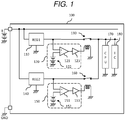
- FIG. 1 is a circuit diagram of a vehicle control device 100 according to a first embodiment of the present invention.
- the vehicle control device 100 is a device that performs processing to control an operation of a vehicle, and includes a first constant voltage generation circuit 110, a first high voltage detection circuit 120, a first switch 130, a second constant voltage generation circuit 140, a second high voltage detection circuit 150, a second switch 160, a CPU 170, and an integrated circuit (IC) 180.
- IC integrated circuit
- the first constant voltage generation circuit 110 receives a supply of a voltage (e.g., 14 V) from an external power supply B, and converts this voltage into a predetermined constant voltage (e.g., 5 V) to output to a load circuit, such as the CPU 170 or the IC 180.
- a voltage e.g. 14 V
- a predetermined constant voltage e.g. 5 V
- the first high voltage detection circuit 120 is a circuit that turns OFF the first switch 130 when the first constant voltage generation circuit 110 generates a voltage that exceeds a first reference voltage.
- the first high voltage detection circuit 120 includes a comparator 121, a first reference voltage source 122, and a buffer 123.
- the first reference voltage source 122 outputs the above-described first reference voltage (e.g., 5.5 V).
- the comparator 121 compares the output voltage from the first constant voltage generation circuit 110 and the first reference voltage outputted from the first reference voltage source 122. When the former is larger, the comparator 121 outputs a driving signal for turning OFF the first switch 130 to the buffer 123.
- the buffer 123 amplifies this driving signal to an appropriate value, to drive the first switch 130.
- the first switch 130 is arranged between an output end of the first constant voltage generation circuit 110 and an input end of each the load circuit, and the output voltage of the first constant voltage generation circuit 110 is supplied to each the load circuit only when the first switch 130 is turned ON.
- the second constant voltage generation circuit 140 is provided with a same function as that of the first constant voltage generation circuit 110.
- the output of the first constant voltage generation circuit 110 and the output of the second constant voltage generation circuit 140 are outputted to the load circuit such as the CPU 170 or the IC 180, via an output circuit described later.
- a rated power of the first constant voltage generation circuit 110 and a rated power of the second constant voltage generation circuit 140 are not necessarily the same, these rated powers are same in the first embodiment, for simplicity of description.
- the second high voltage detection circuit 150 is a circuit that turns OFF the second switch 160 when the second constant voltage generation circuit 140 generates a voltage that exceeds a second reference voltage.
- the second high voltage detection circuit 150 includes a comparator 151, a second reference voltage source 152, and a buffer 153. Each function of these circuits is same as that of each corresponding circuit provided in the first high voltage detection circuit 120.
- the second reference voltage outputted by the second reference voltage source 152 is not necessarily the same as the first reference voltage outputted by the first reference voltage source 122, individual reference voltages are also the same in the first embodiment, considering that the rated powers of the individual constant voltage generation circuits are the same.
- the second switch 160 is arranged between an output end of the second constant voltage generation circuit 140 and the input end of each the load circuit, and the output voltage of the second constant voltage generation circuit 140 is supplied to each the load circuit only when the second switch 160 is turned ON.
- the first switch 130 and the second switch 160 can be configured, for example, by using a component such as an electric relay.
- a component such as an electric relay.
- the configuration is not limited to this, as long as a same operation can be achieved.
- the first constant voltage generation circuit 110 When the external power supply B is supplied to the vehicle control device 100, the first constant voltage generation circuit 110 generates and outputs a specified constant voltage.
- the constant voltage generated by the first constant voltage generation circuit 110 is inputted to the comparator 121.
- the comparator 121 is also inputted with the first reference voltage outputted by the first reference voltage source 122.
- the comparator 121 turns ON the first switch 130. Consequently, the constant voltage generated by the first constant voltage generation circuit 110 is supplied to the CPU 170 and the IC 180.
- the second constant voltage generation circuit 140 When the external power supply B is supplied to the second constant voltage generation circuit 140, the second constant voltage generation circuit 140 generates and outputs a specified constant voltage.
- the constant voltage generated by the second constant voltage generation circuit 140 is inputted to the comparator 151.
- the comparator 151 is also inputted with the second reference voltage outputted by the second reference voltage source 152.
- the comparator 151 turns ON the second switch 160. Consequently, the constant voltage generated by the second constant voltage generation circuit 140 is supplied to the CPU 170 and the IC 180.
- the output end of the first switch 130 and the output end of the second switch 160 are connected to the input end of each the load circuit via the output circuit configured by, for example, a wired OR circuit or the like.
- the output circuit outputs any larger one of the output voltage of the first switch 130 and the output voltage of the second switch 160, to each the load circuit. Therefore, in the normal operation, each the load circuit is supplied with the constant voltages each generated by the first constant voltage generation circuit 110 and the second constant voltage generation circuit 140.
- the voltage generated by the first constant voltage generation circuit 110 drops to less than the specified voltage (e.g., 3 V) due to a cause such as an element failure.
- the outputs of individual constant voltage generation circuits are connected via the output circuit of wired OR that is arranged to each of the output end of the first switch 130 and the output end of the second switch 160. Consequently, even when the constant voltage generated by the first constant voltage generation circuit 110 drops, as long as the constant voltage generated by the second constant voltage generation circuit 140 is normal, a higher one of these voltages (i.e., the output voltage of the second constant voltage generation circuit 140) is supplied to the load circuit. Thus, the vehicle control device 100 can continue the normal operation. The same result is obtained when the output voltage of the second constant voltage generation circuit 140 drops.
- the voltage generated by the first constant voltage generation circuit 110 exceeds the first reference voltage (e.g., 6 V) due to a cause such as an element failure.
- the first reference voltage e.g. 6 V
- the voltage generated by the first constant voltage generation circuit 110 which is higher than the specified voltage, is inputted to the comparator 121. Consequently, the comparator 121 detects that the voltage that exceeds the first reference voltage is inputted, and drives the first switch 130 to turn OFF.
- the first switch 130 is turned OFF, the first constant voltage generation circuit 110 is electrically cut off from the load circuit, and the output voltage of the first constant voltage generation circuit 110 is not supplied to the output circuit any more.
- the constant voltage generated by the second constant voltage generation circuit 140 is supplied to the load circuit via the second switch 160 and the output circuit. Therefore, the vehicle control device 100 can continue the normal operation. The same result is obtained when the output voltage of the second constant voltage generation circuit 140 exceeds the second reference voltage.
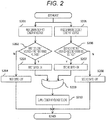
- FIG. 2 is a flowchart illustrating an operational flow of the vehicle control device 100.
- the vehicle control device 100 starts this flowchart when the external power supply B is turned ON. Steps S201 to S204 and steps S205 to S208 are executed in parallel. Each step of FIG. 2 is described below.
- FIG. 2 Steps S201 to S204
- the first constant voltage generation circuit 110 generates a first constant voltage (S201).
- the comparator 121 compares the first constant voltage generated by the first constant voltage generation circuit 110, with the first reference voltage (S202). When the first constant voltage is less than the first reference voltage, the comparator 121 turns ON the first switch 130 (S203). When the first constant voltage is equal to or more than the first reference voltage, the comparator 121 turns OFF the first switch 130 (S204). When the first switch 130 has been turned OFF, the abnormal first constant voltage generated by the first constant voltage generation circuit 110 is not supplied to the output circuit.
- FIG. 2 Steps S205 to S208
- the second constant voltage generation circuit 140 generates a second constant voltage (S205).
- the comparator 151 compares the second constant voltage generated by the second constant voltage generation circuit 140, with the second reference voltage (S206). When the second constant voltage is less than the second reference voltage, the comparator 151 turns ON the second switch 160 (S207). When the second constant voltage is equal to or more than the second reference voltage, the comparator 151 turns OFF the second switch 160 (S208). When the second switch 160 has been turned OFF, the abnormal second constant voltage generated by the second constant voltage generation circuit 140 is not supplied to the output circuit.
- the output voltage of the first switch 130 and the output voltage of the second switch 160 are inputted to the output circuit in parallel (S209).
- the output circuit outputs a higher one of these voltages to the load circuit (S210). When either one of the switches is turned OFF, only an output voltage of another switch is outputted to the load circuit.
- the vehicle control device 100 even when a constant voltage generated by either one of the constant voltage generation circuits is either less than the specified voltage or more than the reference voltage, it is possible to continuously supply a normal constant voltage generated by another constant voltage generation circuit functioning normally, to the load. This can maintain the normal operation of the vehicle control device 100 even if either one of the constant voltage generation circuits has failed.
- the first embodiment is particularly effective for a control device using an arithmetic circuit, such as a CPU 170 or an IC 180, that uses a constant voltage as an operating voltage.
- both the two switches are turned OFF in occurrence of a failure in which both the two constant voltage generation circuits generate voltages that exceed the reference voltage, which eliminates a supply of abnormal high voltage to the load circuit. Therefore, these load circuits can be protected from element destruction.
- FIG. 3 is a circuit diagram of a vehicle control device 100 according to a second embodiment of the present invention.
- a rated power of a first constant voltage generation circuit 110 is larger than a rated power of a second constant voltage generation circuit 140.
- the first high voltage detection circuit 120 detects that the first constant voltage generation circuit 110 generates a larger voltage than a first reference voltage, the first high voltage detection circuit 120 also notifies a CPU 170 about the generation of the voltage. Operation of the CPU 170 is described later. Since other configurations are same as those of the first embodiment, differences are mainly described below.
- the comparator 121 When the comparator 121 detects that the voltage generated by the first constant voltage generation circuit 110 exceeds the first reference voltage, the comparator 121 turns OFF a first switch 130 and notifies the CPU 170 that an abnormality has been detected.
- the CPU 170 When the CPU 170 receives a notification that the first switch 130 has been turned OFF, the CPU 170 changes contents of control processing to perform processing with lower power consumption. This is because the CPU 170 needs to operate by using only a voltage supply from the second constant voltage generation circuit 140, which has a small rated power.
- the CPU 170 can reduce power consumption through a method, for example, such as extending an operation period or shifting to alternate processing with a small operation load. This enables the vehicle control device 100 to continue the normal operation even if only using the second constant voltage generation circuit 140 with the small rated power.
- a detection result of an output voltage of the first constant voltage generation circuit 110 is notified to the CPU 170.
- a detection result of an output voltage of the second constant voltage generation circuit 140 may be notified to the CPU 170, and the CPU 170 may shift to processing with low power consumption. This is because a capability of generating a constant voltage is lowered as a whole vehicle control device 100 when a number of the constant voltage generation circuit operating normally becomes one.
- both the detection results of the individual output voltages of the individual constant voltage generation circuits may be notified to the CPU 170.
- the vehicle control device 100 when the constant voltage generated by any one of the constant voltage generation circuits exceeds the reference voltage, that constant voltage generation circuit is cut off from a load, and the CPU 170 shifts to an operation with small power consumption. This can maintain the operation of the vehicle control device 100 even if a power supply capacity of the constant voltage generation circuit is reduced.
- the rated power of the second constant voltage generation circuit 140 is smaller than the rated power of the first constant voltage generation circuit 110. This can suppress cost of the vehicle control device 100 as compared with when there is provided a plurality of constant voltage generation circuits having equal rated powers.
- FIG. 4 is a circuit diagram of a vehicle control device 100 according to a third embodiment of the present invention.
- a first switch 130 and a second switch 160 are configured by using a semiconductor switch.
- Other configurations are same as those of the first and second embodiments.
- FIG. 4 has exemplified a configuration using the semiconductor switch in a circuit configuration of the first embodiment.
- the semiconductor switch As a switch that cuts off electric conduction between a constant voltage generation circuit and a load circuit, a circuit scale of the vehicle control device 100 can be reduced, and cost can be suppressed, while a same effect as that of the first and second embodiments is provided. Additionally, since the semiconductor switch is easy to mount on a circuit board, it is particularly useful for a device that electronically controls an operation of a vehicle.
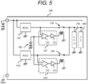
- FIG. 5 is a circuit diagram of a vehicle control device 100 according to a fourth embodiment of the present invention.
- both a first high voltage detection circuit 120 and a second high voltage detection circuit 150 use a common reference voltage source 190 as a reference voltage source.
- the common reference voltage source 190 provides a reference voltage that is used, as a comparison object, by a comparator of each high voltage detection circuit.
- Individual reference voltages may be common, or a reference voltage may be individually provided to each high voltage detection circuit. Other configurations are same as those of the first to third embodiments.
- the common reference voltage source 190 can be configured as a circuit that generates the reference voltage by using its own power source, or can be configured as a circuit that receives a power supply from an external power supply B and converts this into the reference voltage. Moreover, for example, the common reference voltage source 190 can be configured as a circuit that receives a signal specifying a reference voltage value, via a signal input port provided in the vehicle control device 100, and generates the reference voltage according to the specified value.
- the reference voltage source By making the reference voltage source common, a circuit scale of the vehicle control device 100 can be reduced, and cost can be suppressed, while a same effect as that of the first to third embodiments is provided. Additionally, if a circuit specification of a CPU 170, an IC 180, or the like differs depending on types of vehicles, for example, the reference voltage can be flexibly changed according to these specific circuit specifications, by configuring such that the reference voltage is variable.
- FIG. 6 is a circuit diagram of a vehicle control device 100 according to a fifth embodiment of the present invention.
- a first high voltage detection circuit 120 notifies a CPU 170 that the first constant voltage generation circuit 110 generates a voltage that exceeds a specified voltage.
- the CPU 170 stores a log describing the generation of the voltage, in a storage device 171.
- the storage device 171 is, for example, a data-writable memory, such as an electrically erasable and programmable read only memory (EEPROM). Other configurations are same as those of the first to fourth embodiments.
- FIG. 6 has exemplified a configuration provided with the storage device 171 in a circuit configuration of the second embodiment.
- An IC 180 has been omitted for convenience of description.
- a failure cause can be analyzed by analyzing the log stored by the storage device 171.
- Contents of the log include, for example, occurrence date and time of the abnormality, an (abnormal) output voltage value of the constant voltage generation circuit, or the like.
- the present invention is not limited to a form of the above-described embodiments, but also includes various modifications.
- the above embodiments have been described in detail for the purpose of easy explanation of the present invention, and are not necessarily limited to that provided with all the described configurations.
- a part of a configuration of one embodiment can be replaced with a configuration of another embodiment.
- a configuration of one embodiment can be added with a configuration of another embodiment.
- a part of a configuration of each embodiment can be added, deleted, or replaced with another configuration.
- the high voltage detection circuit detects a voltage abnormality by comparing the input voltage and the reference voltage with the comparator in the first to fifth embodiments, a, the configuration of the high voltage detection circuit is not limited to this, and an appropriate circuit configuration that achieves a same function can be used.
- the CPU 170 and the IC 180 have been exemplified as the load circuit. Since the CPU 170 and the IC 180 generally need to be supplied with a constant voltage as an operating voltage, these are suitable for a load circuit supplied with a voltage by the constant voltage generation circuit.
- the load circuit is not limited to these, but can also be other circuit that uses a constant voltage as the operating voltage.
- the first reference voltage is set larger than a rated voltage of the first constant voltage generation circuit 110 (e.g., 5 V), and more preferably, between the rated voltage of the first constant voltage generation circuit 110 and a maximum allowable voltage of the load circuit (e.g., 6 V).
- the second reference voltage is set larger than a rated voltage of the second constant voltage generation circuit 140, and more preferably, between the rated voltage of the second constant voltage generation circuit 140 and the maximum allowable voltage of the load circuit.
- the output end of the first switch 130 and the output end of the second switch 160 are inputted to the output circuit configured by the wired OR circuit.
- the output circuit may be configured by using a configuration other than the wired OR, as long as it is a circuit that outputs any higher one of these output voltages.
- the common reference voltage source 190 is configured to be able to generate the reference voltage itself, or to specify the reference voltage.
- the first reference voltage source 122 and the second reference voltage source 152 can have the same configuration.
Landscapes
- Engineering & Computer Science (AREA)
- Theoretical Computer Science (AREA)
- Physics & Mathematics (AREA)
- General Engineering & Computer Science (AREA)
- General Physics & Mathematics (AREA)
- Power Engineering (AREA)
- Mechanical Engineering (AREA)
- Control Of Eletrric Generators (AREA)
- Electric Propulsion And Braking For Vehicles (AREA)
Abstract
Description
- The present invention relates to a vehicle control device that controls an operation of a vehicle.
- A vehicle control device can control an operation of a vehicle by performing a control operation with an arithmetic logic unit of a microcomputer or a central processing unit (CPU). Since the arithmetic logic unit generally needs to be supplied with a constant voltage, the vehicle control device is provided with a constant voltage generation circuit. The constant voltage generation circuit generally receives a supply of a higher voltage from a power source such as a battery used by the vehicle control device, and converts this voltage into a specified constant voltage to supply to a load circuit, such as the arithmetic logic unit.
-
PTL 1 below discloses a technology relating to a power supply switching circuit that switches a first and second power supplies. InPTL 1, a voltage of the first power supply and a voltage of the second power supply are compared, and a transistor provided between a load and a power supply having a higher voltage is turned ON (refer to Abstract). - PTL 1:
JP 2006-254672 A - In the technology described in
PTL 1 above, it is considered that a specified voltage can be maintained even when an output voltage of either power supply drops to less than the specified voltage. However, in occurrence of an abnormality in which an output voltage of either power supply exceeds the specified voltage, the voltage that exceeds the specified voltage is supplied to the load since a transistor between the load and a power supply having a higher voltage is turned ON, which may cause an abnormal operation of the load. - The present invention has been made in view of the above problem, and it is an object of the present invention to provide a vehicle control device including a plurality of constant voltage generation circuits, in which a specified voltage is supplied to a load even if any one of the constant voltage generation circuits outputs a voltage that exceeds the specified voltage.
- A vehicle control device according to the present invention is provided with a first and second constant voltage generation circuits that each output a voltage to a load, and when either the first or second constant voltage generation circuit outputs a voltage that exceeds a reference voltage, cuts off the output of that constant voltage generation circuit from the load.
- The vehicle control device according to the present invention can continuously supply a specified voltage to the load, even when either the first or second constant voltage generation circuit generates an abnormal voltage that exceeds the specified voltage.
-
- [
FIG. 1] FIG. 1 is a circuit diagram of avehicle control device 100 according to a first embodiment. - [
FIG. 2] FIG. 2 is a flowchart illustrating an operational flow of thevehicle control device 100. - [
FIG. 3] FIG. 3 is a circuit diagram of avehicle control device 100 according to a second embodiment. - [
FIG. 4] FIG. 4 is a circuit diagram of avehicle control device 100 according to a third embodiment. - [
FIG. 5] FIG. 5 is a circuit diagram of avehicle control device 100 according to a fourth embodiment. - [
FIG. 6] FIG. 6 is a circuit diagram of avehicle control device 100 according to a fifth embodiment. -
FIG. 1 is a circuit diagram of avehicle control device 100 according to a first embodiment of the present invention. Thevehicle control device 100 is a device that performs processing to control an operation of a vehicle, and includes a first constantvoltage generation circuit 110, a first highvoltage detection circuit 120, afirst switch 130, a second constantvoltage generation circuit 140, a second highvoltage detection circuit 150, asecond switch 160, aCPU 170, and an integrated circuit (IC) 180. - The first constant
voltage generation circuit 110 receives a supply of a voltage (e.g., 14 V) from an external power supply B, and converts this voltage into a predetermined constant voltage (e.g., 5 V) to output to a load circuit, such as theCPU 170 or theIC 180. - The first high
voltage detection circuit 120 is a circuit that turns OFF thefirst switch 130 when the first constantvoltage generation circuit 110 generates a voltage that exceeds a first reference voltage. The first highvoltage detection circuit 120 includes acomparator 121, a firstreference voltage source 122, and abuffer 123. - The first
reference voltage source 122 outputs the above-described first reference voltage (e.g., 5.5 V). Thecomparator 121 compares the output voltage from the first constantvoltage generation circuit 110 and the first reference voltage outputted from the firstreference voltage source 122. When the former is larger, thecomparator 121 outputs a driving signal for turning OFF thefirst switch 130 to thebuffer 123. Thebuffer 123 amplifies this driving signal to an appropriate value, to drive thefirst switch 130. - The
first switch 130 is arranged between an output end of the first constantvoltage generation circuit 110 and an input end of each the load circuit, and the output voltage of the first constantvoltage generation circuit 110 is supplied to each the load circuit only when thefirst switch 130 is turned ON. - The second constant
voltage generation circuit 140 is provided with a same function as that of the first constantvoltage generation circuit 110. The output of the first constantvoltage generation circuit 110 and the output of the second constantvoltage generation circuit 140 are outputted to the load circuit such as theCPU 170 or theIC 180, via an output circuit described later. Although a rated power of the first constantvoltage generation circuit 110 and a rated power of the second constantvoltage generation circuit 140 are not necessarily the same, these rated powers are same in the first embodiment, for simplicity of description. - The second high
voltage detection circuit 150 is a circuit that turns OFF thesecond switch 160 when the second constantvoltage generation circuit 140 generates a voltage that exceeds a second reference voltage. The second highvoltage detection circuit 150 includes acomparator 151, a secondreference voltage source 152, and abuffer 153. Each function of these circuits is same as that of each corresponding circuit provided in the first highvoltage detection circuit 120. Although the second reference voltage outputted by the secondreference voltage source 152 is not necessarily the same as the first reference voltage outputted by the firstreference voltage source 122, individual reference voltages are also the same in the first embodiment, considering that the rated powers of the individual constant voltage generation circuits are the same. - The
second switch 160 is arranged between an output end of the second constantvoltage generation circuit 140 and the input end of each the load circuit, and the output voltage of the second constantvoltage generation circuit 140 is supplied to each the load circuit only when thesecond switch 160 is turned ON. - The
first switch 130 and thesecond switch 160 can be configured, for example, by using a component such as an electric relay. However, the configuration is not limited to this, as long as a same operation can be achieved. - When the external power supply B is supplied to the
vehicle control device 100, the first constantvoltage generation circuit 110 generates and outputs a specified constant voltage. The constant voltage generated by the first constantvoltage generation circuit 110 is inputted to thecomparator 121. Thecomparator 121 is also inputted with the first reference voltage outputted by the firstreference voltage source 122. When the constant voltage inputted to thecomparator 121 is equal to or less than the first reference voltage, thecomparator 121 turns ON thefirst switch 130. Consequently, the constant voltage generated by the first constantvoltage generation circuit 110 is supplied to theCPU 170 and theIC 180. - When the external power supply B is supplied to the second constant
voltage generation circuit 140, the second constantvoltage generation circuit 140 generates and outputs a specified constant voltage. The constant voltage generated by the second constantvoltage generation circuit 140 is inputted to thecomparator 151. Thecomparator 151 is also inputted with the second reference voltage outputted by the secondreference voltage source 152. When the constant voltage inputted to thecomparator 151 is equal to or less than the second reference voltage, thecomparator 151 turns ON thesecond switch 160. Consequently, the constant voltage generated by the second constantvoltage generation circuit 140 is supplied to theCPU 170 and theIC 180. - The output end of the
first switch 130 and the output end of thesecond switch 160 are connected to the input end of each the load circuit via the output circuit configured by, for example, a wired OR circuit or the like. The output circuit outputs any larger one of the output voltage of thefirst switch 130 and the output voltage of thesecond switch 160, to each the load circuit. Therefore, in the normal operation, each the load circuit is supplied with the constant voltages each generated by the first constantvoltage generation circuit 110 and the second constantvoltage generation circuit 140. - It is assumed that the voltage generated by the first constant
voltage generation circuit 110 drops to less than the specified voltage (e.g., 3 V) due to a cause such as an element failure. - The outputs of individual constant voltage generation circuits are connected via the output circuit of wired OR that is arranged to each of the output end of the
first switch 130 and the output end of thesecond switch 160. Consequently, even when the constant voltage generated by the first constantvoltage generation circuit 110 drops, as long as the constant voltage generated by the second constantvoltage generation circuit 140 is normal, a higher one of these voltages (i.e., the output voltage of the second constant voltage generation circuit 140) is supplied to the load circuit. Thus, thevehicle control device 100 can continue the normal operation. The same result is obtained when the output voltage of the second constantvoltage generation circuit 140 drops. - It is assumed that the voltage generated by the first constant
voltage generation circuit 110 exceeds the first reference voltage (e.g., 6 V) due to a cause such as an element failure. - The voltage generated by the first constant
voltage generation circuit 110, which is higher than the specified voltage, is inputted to thecomparator 121. Consequently, thecomparator 121 detects that the voltage that exceeds the first reference voltage is inputted, and drives thefirst switch 130 to turn OFF. When thefirst switch 130 is turned OFF, the first constantvoltage generation circuit 110 is electrically cut off from the load circuit, and the output voltage of the first constantvoltage generation circuit 110 is not supplied to the output circuit any more. Whereas, the constant voltage generated by the second constantvoltage generation circuit 140 is supplied to the load circuit via thesecond switch 160 and the output circuit. Therefore, thevehicle control device 100 can continue the normal operation. The same result is obtained when the output voltage of the second constantvoltage generation circuit 140 exceeds the second reference voltage. -
FIG. 2 is a flowchart illustrating an operational flow of thevehicle control device 100. Thevehicle control device 100 starts this flowchart when the external power supply B is turned ON. Steps S201 to S204 and steps S205 to S208 are executed in parallel. Each step ofFIG. 2 is described below. - The first constant
voltage generation circuit 110 generates a first constant voltage (S201). Thecomparator 121 compares the first constant voltage generated by the first constantvoltage generation circuit 110, with the first reference voltage (S202). When the first constant voltage is less than the first reference voltage, thecomparator 121 turns ON the first switch 130 (S203). When the first constant voltage is equal to or more than the first reference voltage, thecomparator 121 turns OFF the first switch 130 (S204). When thefirst switch 130 has been turned OFF, the abnormal first constant voltage generated by the first constantvoltage generation circuit 110 is not supplied to the output circuit. - The second constant
voltage generation circuit 140 generates a second constant voltage (S205). Thecomparator 151 compares the second constant voltage generated by the second constantvoltage generation circuit 140, with the second reference voltage (S206). When the second constant voltage is less than the second reference voltage, thecomparator 151 turns ON the second switch 160 (S207). When the second constant voltage is equal to or more than the second reference voltage, thecomparator 151 turns OFF the second switch 160 (S208). When thesecond switch 160 has been turned OFF, the abnormal second constant voltage generated by the second constantvoltage generation circuit 140 is not supplied to the output circuit. - The output voltage of the
first switch 130 and the output voltage of thesecond switch 160 are inputted to the output circuit in parallel (S209). The output circuit outputs a higher one of these voltages to the load circuit (S210). When either one of the switches is turned OFF, only an output voltage of another switch is outputted to the load circuit. - In the
vehicle control device 100 according to the first embodiment, even when a constant voltage generated by either one of the constant voltage generation circuits is either less than the specified voltage or more than the reference voltage, it is possible to continuously supply a normal constant voltage generated by another constant voltage generation circuit functioning normally, to the load. This can maintain the normal operation of thevehicle control device 100 even if either one of the constant voltage generation circuits has failed. The first embodiment is particularly effective for a control device using an arithmetic circuit, such as aCPU 170 or anIC 180, that uses a constant voltage as an operating voltage. - In the first embodiment, both the two switches are turned OFF in occurrence of a failure in which both the two constant voltage generation circuits generate voltages that exceed the reference voltage, which eliminates a supply of abnormal high voltage to the load circuit. Therefore, these load circuits can be protected from element destruction.
- Although the configuration including two constant voltage generation circuits has been described in the first embodiment, the same function as that of the first embodiment can be achieved even when there are three or more constant voltage generation circuits, by inputting output voltages of the constant voltage generation circuits to an OR output circuit via a switch. The same result is obtained in the following embodiments.
- Although there has been described the operation where one of the constant voltage generation circuits has failed in the first embodiment, the same function as that of the first embodiment can be achieved even if a plurality of constant voltage generation circuits have failed while there are three or more constant voltage generation circuits, as long as at least one constant voltage generation circuit operates normally. The same result is obtained in the following embodiments.
-
FIG. 3 is a circuit diagram of avehicle control device 100 according to a second embodiment of the present invention. In the second embodiment, a rated power of a first constantvoltage generation circuit 110 is larger than a rated power of a second constantvoltage generation circuit 140. Additionally, in the second embodiment, when a first highvoltage detection circuit 120 detects that the first constantvoltage generation circuit 110 generates a larger voltage than a first reference voltage, the first highvoltage detection circuit 120 also notifies aCPU 170 about the generation of the voltage. Operation of theCPU 170 is described later. Since other configurations are same as those of the first embodiment, differences are mainly described below. - When the
comparator 121 detects that the voltage generated by the first constantvoltage generation circuit 110 exceeds the first reference voltage, thecomparator 121 turns OFF afirst switch 130 and notifies theCPU 170 that an abnormality has been detected. - When the
CPU 170 receives a notification that thefirst switch 130 has been turned OFF, theCPU 170 changes contents of control processing to perform processing with lower power consumption. This is because theCPU 170 needs to operate by using only a voltage supply from the second constantvoltage generation circuit 140, which has a small rated power. TheCPU 170 can reduce power consumption through a method, for example, such as extending an operation period or shifting to alternate processing with a small operation load. This enables thevehicle control device 100 to continue the normal operation even if only using the second constantvoltage generation circuit 140 with the small rated power. - In
FIG. 3 , a detection result of an output voltage of the first constantvoltage generation circuit 110 is notified to theCPU 170. Alternatively, a detection result of an output voltage of the second constantvoltage generation circuit 140 may be notified to theCPU 170, and theCPU 170 may shift to processing with low power consumption. This is because a capability of generating a constant voltage is lowered as a wholevehicle control device 100 when a number of the constant voltage generation circuit operating normally becomes one. Alternatively, both the detection results of the individual output voltages of the individual constant voltage generation circuits may be notified to theCPU 170. - In the
vehicle control device 100 according to the second embodiment, when the constant voltage generated by any one of the constant voltage generation circuits exceeds the reference voltage, that constant voltage generation circuit is cut off from a load, and theCPU 170 shifts to an operation with small power consumption. This can maintain the operation of thevehicle control device 100 even if a power supply capacity of the constant voltage generation circuit is reduced. - In the
vehicle control device 100 according to the second embodiment, the rated power of the second constantvoltage generation circuit 140 is smaller than the rated power of the first constantvoltage generation circuit 110. This can suppress cost of thevehicle control device 100 as compared with when there is provided a plurality of constant voltage generation circuits having equal rated powers. -
FIG. 4 is a circuit diagram of avehicle control device 100 according to a third embodiment of the present invention. In the third embodiment, either or both of afirst switch 130 and asecond switch 160 are configured by using a semiconductor switch. Other configurations are same as those of the first and second embodiments.FIG. 4 has exemplified a configuration using the semiconductor switch in a circuit configuration of the first embodiment. - By using the semiconductor switch as a switch that cuts off electric conduction between a constant voltage generation circuit and a load circuit, a circuit scale of the
vehicle control device 100 can be reduced, and cost can be suppressed, while a same effect as that of the first and second embodiments is provided. Additionally, since the semiconductor switch is easy to mount on a circuit board, it is particularly useful for a device that electronically controls an operation of a vehicle. -
FIG. 5 is a circuit diagram of avehicle control device 100 according to a fourth embodiment of the present invention. In the fourth embodiment, both a first highvoltage detection circuit 120 and a second highvoltage detection circuit 150 use a commonreference voltage source 190 as a reference voltage source. The commonreference voltage source 190 provides a reference voltage that is used, as a comparison object, by a comparator of each high voltage detection circuit. Individual reference voltages may be common, or a reference voltage may be individually provided to each high voltage detection circuit. Other configurations are same as those of the first to third embodiments. - The common
reference voltage source 190 can be configured as a circuit that generates the reference voltage by using its own power source, or can be configured as a circuit that receives a power supply from an external power supply B and converts this into the reference voltage. Moreover, for example, the commonreference voltage source 190 can be configured as a circuit that receives a signal specifying a reference voltage value, via a signal input port provided in thevehicle control device 100, and generates the reference voltage according to the specified value. - By making the reference voltage source common, a circuit scale of the
vehicle control device 100 can be reduced, and cost can be suppressed, while a same effect as that of the first to third embodiments is provided. Additionally, if a circuit specification of aCPU 170, anIC 180, or the like differs depending on types of vehicles, for example, the reference voltage can be flexibly changed according to these specific circuit specifications, by configuring such that the reference voltage is variable. -
FIG. 6 is a circuit diagram of avehicle control device 100 according to a fifth embodiment of the present invention. In the fifth embodiment, a first highvoltage detection circuit 120 notifies aCPU 170 that the first constantvoltage generation circuit 110 generates a voltage that exceeds a specified voltage. TheCPU 170 stores a log describing the generation of the voltage, in astorage device 171. Thestorage device 171 is, for example, a data-writable memory, such as an electrically erasable and programmable read only memory (EEPROM). Other configurations are same as those of the first to fourth embodiments.FIG. 6 has exemplified a configuration provided with thestorage device 171 in a circuit configuration of the second embodiment. AnIC 180 has been omitted for convenience of description. - According to the fifth embodiment, if the constant voltage generation circuit generates an abnormal high voltage, a failure cause can be analyzed by analyzing the log stored by the
storage device 171. Contents of the log include, for example, occurrence date and time of the abnormality, an (abnormal) output voltage value of the constant voltage generation circuit, or the like. - The present invention is not limited to a form of the above-described embodiments, but also includes various modifications. The above embodiments have been described in detail for the purpose of easy explanation of the present invention, and are not necessarily limited to that provided with all the described configurations. Moreover, a part of a configuration of one embodiment can be replaced with a configuration of another embodiment. Further, a configuration of one embodiment can be added with a configuration of another embodiment. Furthermore, a part of a configuration of each embodiment can be added, deleted, or replaced with another configuration.
- Although it has been described that the high voltage detection circuit detects a voltage abnormality by comparing the input voltage and the reference voltage with the comparator in the first to fifth embodiments, a, the configuration of the high voltage detection circuit is not limited to this, and an appropriate circuit configuration that achieves a same function can be used.
- In the first to fifth embodiments, the
CPU 170 and theIC 180 have been exemplified as the load circuit. Since theCPU 170 and theIC 180 generally need to be supplied with a constant voltage as an operating voltage, these are suitable for a load circuit supplied with a voltage by the constant voltage generation circuit. However, the load circuit is not limited to these, but can also be other circuit that uses a constant voltage as the operating voltage. - In the first to fifth embodiments, the first reference voltage is set larger than a rated voltage of the first constant voltage generation circuit 110 (e.g., 5 V), and more preferably, between the rated voltage of the first constant
voltage generation circuit 110 and a maximum allowable voltage of the load circuit (e.g., 6 V). The second reference voltage is set larger than a rated voltage of the second constantvoltage generation circuit 140, and more preferably, between the rated voltage of the second constantvoltage generation circuit 140 and the maximum allowable voltage of the load circuit. - It has been described that, in the first to fifth embodiments, the output end of the
first switch 130 and the output end of thesecond switch 160 are inputted to the output circuit configured by the wired OR circuit. The output circuit may be configured by using a configuration other than the wired OR, as long as it is a circuit that outputs any higher one of these output voltages. - It has been described that, in the fourth embodiment, the common
reference voltage source 190 is configured to be able to generate the reference voltage itself, or to specify the reference voltage. The firstreference voltage source 122 and the secondreference voltage source 152 can have the same configuration. -
- 100
- vehicle control device
- 110
- first constant voltage generation circuit
- 120
- first high voltage detection circuit
- 130
- first switch
- 140
- second constant voltage generation circuit
- 150
- second high voltage detection circuit
- 160
- second switch
- 170
- CPU
- 171
- storage device
- 180
- IC
Claims (9)
- A vehicle control device that controls an operation of a vehicle, the vehicle control device comprising:a first and a second constant voltage generation circuits that each output a constant voltage to a circuit that performs processing to control the operation of the vehicle;a first high voltage detection circuit that detects that the first constant voltage generation circuit has outputted a voltage equal to or more than a first reference voltage;a second high voltage detection circuit that detects that the second constant voltage generation circuit has outputted a voltage equal to or more than a second reference voltage;a first switch that is arranged between the circuit and the first constant voltage generation circuit, and cuts off a voltage output to the circuit from the first constant voltage generation circuit when the first high voltage detection circuit detects that the first constant voltage generation circuit has outputted a voltage equal to or more than the first reference voltage;a second switch that is arranged between the circuit and the second constant voltage generation circuit, and cuts off a voltage output to the circuit from the second constant voltage generation circuit when the second high voltage detection circuit detects that the second constant voltage generation circuit has outputted a voltage equal to or more than the second reference voltage; andan output circuit that outputs any larger one of an output voltage of the first switch and an output voltage of the second switch, to the circuit, whereinthe first reference voltage is larger than a rated voltage of the first constant voltage generation circuit, andthe second reference voltage is larger than a rated voltage of the second constant voltage generation circuit.
- The vehicle control device according to claim 1, wherein
a rated power of the first constant voltage generation circuit is different from a rated power of the second constant voltage generation circuit,
at least either one of the first high voltage detection circuit and the second high voltage detection circuit is configured to output a detection result to the circuit, and
when the circuit receives, from the first high voltage detection circuit, a detection result that the first constant voltage generation circuit has outputted a voltage equal to or more than the first reference voltage, or when the circuit receives, from the second high voltage detection circuit, a detection result that the second constant voltage generation circuit has outputted a voltage equal to or more than the second reference voltage, the circuit adjusts power consumption of the circuit according to the detection result. - The vehicle control device according to claim 2, wherein
the rated power of the first constant voltage generation circuit is larger than the rated power of the second constant voltage generation circuit,
the first high voltage detection circuit is configured to output a detection result to the circuit, and
when the circuit receives, from the first high voltage detection circuit, the detection result that the first constant voltage generation circuit has outputted a voltage equal to or more than the first reference voltage, the circuit changes contents of the processing so as to reduce the power consumption of the circuit. - The vehicle control device according to claim 1, wherein
at least either one of the first switch and the second switch is a switch configured by a semiconductor device. - The vehicle control device according to claim 1, wherein
the vehicle control device comprises a reference voltage source that supplies the first reference voltage to the first high voltage detection circuit and also supplies the second reference voltage to the second high voltage detection circuit, and
the reference voltage source supplies the first reference voltage and the second reference voltage that have a same voltage value, respectively to the first high voltage detection circuit and the second high voltage detection circuit. - The vehicle control device according to claim 1, comprising:a first reference voltage source that supplies the first reference voltage to the first high voltage detection circuit; anda second reference voltage source that supplies the second reference voltage to the second high voltage detection circuit, whereinthe first reference voltage source is configured to be able to specify the first reference voltage via a signal input port provided in the vehicle control device, andthe second reference voltage source is configured to be able to specify the second reference voltage via a signal input port provided in the vehicle control device.
- The vehicle control device according to claim 1, comprising:a first reference voltage source that supplies the first reference voltage to the first high voltage detection circuit; anda second reference voltage source that supplies the second reference voltage to the second high voltage detection circuit, whereinthe first reference voltage source is configured to generate the first reference voltage by using a power source supplied to the vehicle control device, andthe second reference voltage source is configured to generate the second reference voltage by using the power source supplied to the vehicle control device.
- The vehicle control device according to claim 1, wherein
the first reference voltage is set between the rated voltage of the first constant voltage generation circuit and a maximum allowable voltage of the circuit; and
the second reference voltage is set between the rated voltage of the second constant voltage generation circuit and the maximum allowable voltage of the circuit. - The vehicle control device according to claim 1, wherein
the vehicle control device comprises a memory that stores data describing a detection result of the first high voltage detection circuit and a detection result of the second high voltage detection circuit.
Applications Claiming Priority (2)
| Application Number | Priority Date | Filing Date | Title |
|---|---|---|---|
| JP2015020968 | 2015-02-05 | ||
| PCT/JP2016/052569 WO2016125690A1 (en) | 2015-02-05 | 2016-01-29 | Vehicle control device |
Publications (3)
| Publication Number | Publication Date |
|---|---|
| EP3254904A1 true EP3254904A1 (en) | 2017-12-13 |
| EP3254904A4 EP3254904A4 (en) | 2018-06-20 |
| EP3254904B1 EP3254904B1 (en) | 2020-07-22 |
Family
ID=56564037
Family Applications (1)
| Application Number | Title | Priority Date | Filing Date |
|---|---|---|---|
| EP16746521.0A Active EP3254904B1 (en) | 2015-02-05 | 2016-01-29 | Vehicle control device |
Country Status (5)
| Country | Link |
|---|---|
| US (1) | US10427626B2 (en) |
| EP (1) | EP3254904B1 (en) |
| JP (1) | JP6426208B2 (en) |
| CN (1) | CN107107842B (en) |
| WO (1) | WO2016125690A1 (en) |
Families Citing this family (1)
| Publication number | Priority date | Publication date | Assignee | Title |
|---|---|---|---|---|
| JP7271970B2 (en) * | 2019-01-31 | 2023-05-12 | 株式会社アドヴィックス | Control device |
Family Cites Families (36)
| Publication number | Priority date | Publication date | Assignee | Title |
|---|---|---|---|---|
| JPH05189065A (en) * | 1992-01-10 | 1993-07-30 | Fujitsu Ltd | Detection system for overvoltage in parallel operation |
| JPH0795734A (en) * | 1993-08-26 | 1995-04-07 | Fujitsu Ten Ltd | Power supply circuit |
| JPH10108363A (en) * | 1996-09-25 | 1998-04-24 | Sony Corp | Parallel operation power supply system |
| JP3119599B2 (en) * | 1997-06-12 | 2000-12-25 | 日本電気アイシーマイコンシステム株式会社 | Power supply circuit |
| JP3394509B2 (en) * | 1999-08-06 | 2003-04-07 | 株式会社リコー | Constant voltage power supply |
| JP2002218668A (en) * | 2001-01-19 | 2002-08-02 | Fujitsu Ltd | Portable information processing device, charging device and method |
| JP2002341978A (en) * | 2001-05-11 | 2002-11-29 | Furukawa Electric Co Ltd:The | Electronic control unit |
| JP3541826B2 (en) * | 2001-09-21 | 2004-07-14 | セイコーエプソン株式会社 | Power supply circuit and control method thereof |
| JP2004062331A (en) * | 2002-07-25 | 2004-02-26 | Ricoh Co Ltd | DC power supply |
| WO2005065347A2 (en) * | 2003-12-29 | 2005-07-21 | Sherwood Information Partners, Inc. | System and method for mass storage using multiple-hard-disk-drive enclosure |
| JP2006254672A (en) | 2005-03-14 | 2006-09-21 | Mitsumi Electric Co Ltd | Power supply switching circuit |
| JP4222337B2 (en) * | 2005-04-04 | 2009-02-12 | トヨタ自動車株式会社 | Power supply system having a plurality of power supplies and vehicle having the same |
| DE102005026998A1 (en) * | 2005-06-10 | 2006-12-14 | Siemens Ag | Arrangement with a recording device |
| JP4379412B2 (en) * | 2005-12-05 | 2009-12-09 | トヨタ自動車株式会社 | Power steering power control device |
| US20070150765A1 (en) * | 2005-12-26 | 2007-06-28 | Takayuki Ochiai | Information processing apparatus having electronic device whose operating speed is controlled, and method of controlling the operating speed of the electronic device |
| JP4459918B2 (en) * | 2006-03-16 | 2010-04-28 | 富士通テン株式会社 | Switching regulator |
| JP2007286937A (en) * | 2006-04-18 | 2007-11-01 | Hitachi Ltd | Storage device and storage device power failure management method |
| JP2008225952A (en) * | 2007-03-14 | 2008-09-25 | Ricoh Co Ltd | Voltage regulator |
| JP4750747B2 (en) * | 2007-04-09 | 2011-08-17 | キヤノン株式会社 | Storage device, storage device control method, and control device |
| US7719134B2 (en) * | 2007-06-12 | 2010-05-18 | Mitsubishi Electric Corporation | In-vehicle mount electronic controller |
| JP2009080597A (en) * | 2007-09-26 | 2009-04-16 | Oki Data Corp | Information processing device |
| JP4535298B2 (en) * | 2008-04-07 | 2010-09-01 | トヨタ自動車株式会社 | Vehicle power supply |
| JP2010108411A (en) * | 2008-10-31 | 2010-05-13 | Toshiba Corp | Disk array control apparatus and information processing apparatus |
| JP5228971B2 (en) * | 2009-02-12 | 2013-07-03 | ブラザー工業株式会社 | Power circuit |
| US8598734B2 (en) * | 2009-05-08 | 2013-12-03 | Toyota Jidosha Kabushiki Kaisha | Power supply system and vehicle equipped with the same |
| JP2011024305A (en) * | 2009-07-14 | 2011-02-03 | Sharp Corp | Parallel drive power supply |
| JP2011162147A (en) * | 2010-02-15 | 2011-08-25 | Autonetworks Technologies Ltd | Vehicular power source supply device and vehicular control device |
| JP5790197B2 (en) * | 2011-06-24 | 2015-10-07 | 株式会社リコー | Image forming apparatus and power supply control method |
| JP5927300B2 (en) * | 2011-09-09 | 2016-06-01 | 景信 丁 | Power management device |
| US9225158B2 (en) * | 2011-09-14 | 2015-12-29 | Denso Corporation | Overcurrent protection circuit |
| JP2013126361A (en) * | 2011-12-16 | 2013-06-24 | Hitachi Automotive Systems Ltd | In-vehicle electronic control unit |
| JP5944172B2 (en) * | 2012-01-31 | 2016-07-05 | 富士通テン株式会社 | Power circuit |
| JP5820779B2 (en) * | 2012-07-06 | 2015-11-24 | 日立オートモティブシステムズ株式会社 | In-vehicle power supply |
| JP6060034B2 (en) * | 2013-04-30 | 2017-01-11 | 株式会社ユーシン | Touch switch and operation panel |
| JP6267052B2 (en) * | 2013-09-27 | 2018-01-24 | ルネサスエレクトロニクス株式会社 | Power supply circuit and control method of power supply circuit |
| JP6249741B2 (en) * | 2013-11-29 | 2017-12-20 | キヤノン株式会社 | Information processing apparatus and control method of information processing apparatus |
-
2016
- 2016-01-29 US US15/544,104 patent/US10427626B2/en active Active
- 2016-01-29 EP EP16746521.0A patent/EP3254904B1/en active Active
- 2016-01-29 WO PCT/JP2016/052569 patent/WO2016125690A1/en not_active Ceased
- 2016-01-29 CN CN201680004328.8A patent/CN107107842B/en active Active
- 2016-01-29 JP JP2016573322A patent/JP6426208B2/en active Active
Also Published As
| Publication number | Publication date |
|---|---|
| JPWO2016125690A1 (en) | 2017-09-21 |
| CN107107842A (en) | 2017-08-29 |
| CN107107842B (en) | 2019-08-23 |
| EP3254904A4 (en) | 2018-06-20 |
| EP3254904B1 (en) | 2020-07-22 |
| US10427626B2 (en) | 2019-10-01 |
| JP6426208B2 (en) | 2018-11-21 |
| WO2016125690A1 (en) | 2016-08-11 |
| US20170361787A1 (en) | 2017-12-21 |
Similar Documents
| Publication | Publication Date | Title |
|---|---|---|
| JP5840975B2 (en) | Gate drive circuit | |
| KR20110118824A (en) | Uninterruptible power system | |
| JP5406443B2 (en) | Overvoltage protection circuit | |
| JP4978491B2 (en) | Power supply system and element failure detection method | |
| US8766679B1 (en) | Power on reset (POR) circuit | |
| US11139653B2 (en) | System power supply circuit | |
| US9985445B2 (en) | Charging/discharging control circuit, charging/discharging control device, and battery apparatus | |
| KR102338808B1 (en) | Voltage abnormal detection circuit and semiconductor device | |
| US10198329B2 (en) | Power supply device | |
| US8977406B2 (en) | Power supply system, power supply control method, power supply control device and program | |
| JP6079923B2 (en) | Power supply system, control method, and control program | |
| EP3254904B1 (en) | Vehicle control device | |
| JP2013196626A (en) | Power supply system, control method and control program | |
| US11842776B2 (en) | Memory system and method of controlling power therein | |
| KR101446929B1 (en) | System for controlling power-up sequence | |
| KR101702081B1 (en) | Double Power Supply | |
| US10627884B2 (en) | Semiconductor device, power-supply system, and controlling method of semiconductor device | |
| JP2013126361A (en) | In-vehicle electronic control unit | |
| KR102514585B1 (en) | Digital protection relay and controlling method thereof | |
| JP2015142452A (en) | Motor drive device | |
| US7475268B2 (en) | Method for managing voltage supply in multiple linked systems | |
| JP2011061968A (en) | Power supply monitoring circuit, power supply monitoring method used for the same, power supply monitoring control program, and electronic apparatus | |
| JP2006223042A (en) | Apparatus and method for parallel operation of inverter system | |
| JP6090103B2 (en) | Power supply | |
| JP2021100321A (en) | Power supply device, information processing system, method for determining by power supply device, and program |
Legal Events
| Date | Code | Title | Description |
|---|---|---|---|
| STAA | Information on the status of an ep patent application or granted ep patent |
Free format text: STATUS: THE INTERNATIONAL PUBLICATION HAS BEEN MADE |
|
| PUAI | Public reference made under article 153(3) epc to a published international application that has entered the european phase |
Free format text: ORIGINAL CODE: 0009012 |
|
| STAA | Information on the status of an ep patent application or granted ep patent |
Free format text: STATUS: REQUEST FOR EXAMINATION WAS MADE |
|
| 17P | Request for examination filed |
Effective date: 20170905 |
|
| AK | Designated contracting states |
Kind code of ref document: A1 Designated state(s): AL AT BE BG CH CY CZ DE DK EE ES FI FR GB GR HR HU IE IS IT LI LT LU LV MC MK MT NL NO PL PT RO RS SE SI SK SM TR |
|
| AX | Request for extension of the european patent |
Extension state: BA ME |
|
| DAV | Request for validation of the european patent (deleted) | ||
| DAX | Request for extension of the european patent (deleted) | ||
| A4 | Supplementary search report drawn up and despatched |
Effective date: 20180524 |
|
| RIC1 | Information provided on ipc code assigned before grant |
Ipc: G06F 1/26 20060101ALI20180517BHEP Ipc: H02J 1/00 20060101ALI20180517BHEP Ipc: H02J 1/10 20060101ALI20180517BHEP Ipc: B60R 16/03 20060101ALI20180517BHEP Ipc: B60R 16/02 20060101AFI20180517BHEP |
|
| STAA | Information on the status of an ep patent application or granted ep patent |
Free format text: STATUS: EXAMINATION IS IN PROGRESS |
|
| 17Q | First examination report despatched |
Effective date: 20190130 |
|
| GRAP | Despatch of communication of intention to grant a patent |
Free format text: ORIGINAL CODE: EPIDOSNIGR1 |
|
| STAA | Information on the status of an ep patent application or granted ep patent |
Free format text: STATUS: GRANT OF PATENT IS INTENDED |
|
| INTG | Intention to grant announced |
Effective date: 20200225 |
|
| GRAS | Grant fee paid |
Free format text: ORIGINAL CODE: EPIDOSNIGR3 |
|
| GRAA | (expected) grant |
Free format text: ORIGINAL CODE: 0009210 |
|
| STAA | Information on the status of an ep patent application or granted ep patent |
Free format text: STATUS: THE PATENT HAS BEEN GRANTED |
|
| AK | Designated contracting states |
Kind code of ref document: B1 Designated state(s): AL AT BE BG CH CY CZ DE DK EE ES FI FR GB GR HR HU IE IS IT LI LT LU LV MC MK MT NL NO PL PT RO RS SE SI SK SM TR |
|
| REG | Reference to a national code |
Ref country code: GB Ref legal event code: FG4D |
|
| REG | Reference to a national code |
Ref country code: CH Ref legal event code: EP |
|
| REG | Reference to a national code |
Ref country code: DE Ref legal event code: R096 Ref document number: 602016040419 Country of ref document: DE |
|
| REG | Reference to a national code |
Ref country code: AT Ref legal event code: REF Ref document number: 1293091 Country of ref document: AT Kind code of ref document: T Effective date: 20200815 |
|
| REG | Reference to a national code |
Ref country code: IE Ref legal event code: FG4D |
|
| REG | Reference to a national code |
Ref country code: LT Ref legal event code: MG4D |
|
| REG | Reference to a national code |
Ref country code: AT Ref legal event code: MK05 Ref document number: 1293091 Country of ref document: AT Kind code of ref document: T Effective date: 20200722 |
|
| PG25 | Lapsed in a contracting state [announced via postgrant information from national office to epo] |
Ref country code: LT Free format text: LAPSE BECAUSE OF FAILURE TO SUBMIT A TRANSLATION OF THE DESCRIPTION OR TO PAY THE FEE WITHIN THE PRESCRIBED TIME-LIMIT Effective date: 20200722 Ref country code: ES Free format text: LAPSE BECAUSE OF FAILURE TO SUBMIT A TRANSLATION OF THE DESCRIPTION OR TO PAY THE FEE WITHIN THE PRESCRIBED TIME-LIMIT Effective date: 20200722 Ref country code: BG Free format text: LAPSE BECAUSE OF FAILURE TO SUBMIT A TRANSLATION OF THE DESCRIPTION OR TO PAY THE FEE WITHIN THE PRESCRIBED TIME-LIMIT Effective date: 20201022 Ref country code: HR Free format text: LAPSE BECAUSE OF FAILURE TO SUBMIT A TRANSLATION OF THE DESCRIPTION OR TO PAY THE FEE WITHIN THE PRESCRIBED TIME-LIMIT Effective date: 20200722 Ref country code: AT Free format text: LAPSE BECAUSE OF FAILURE TO SUBMIT A TRANSLATION OF THE DESCRIPTION OR TO PAY THE FEE WITHIN THE PRESCRIBED TIME-LIMIT Effective date: 20200722 Ref country code: PT Free format text: LAPSE BECAUSE OF FAILURE TO SUBMIT A TRANSLATION OF THE DESCRIPTION OR TO PAY THE FEE WITHIN THE PRESCRIBED TIME-LIMIT Effective date: 20201123 Ref country code: FI Free format text: LAPSE BECAUSE OF FAILURE TO SUBMIT A TRANSLATION OF THE DESCRIPTION OR TO PAY THE FEE WITHIN THE PRESCRIBED TIME-LIMIT Effective date: 20200722 Ref country code: NO Free format text: LAPSE BECAUSE OF FAILURE TO SUBMIT A TRANSLATION OF THE DESCRIPTION OR TO PAY THE FEE WITHIN THE PRESCRIBED TIME-LIMIT Effective date: 20201022 Ref country code: SE Free format text: LAPSE BECAUSE OF FAILURE TO SUBMIT A TRANSLATION OF THE DESCRIPTION OR TO PAY THE FEE WITHIN THE PRESCRIBED TIME-LIMIT Effective date: 20200722 Ref country code: GR Free format text: LAPSE BECAUSE OF FAILURE TO SUBMIT A TRANSLATION OF THE DESCRIPTION OR TO PAY THE FEE WITHIN THE PRESCRIBED TIME-LIMIT Effective date: 20201023 |
|
| PG25 | Lapsed in a contracting state [announced via postgrant information from national office to epo] |
Ref country code: IS Free format text: LAPSE BECAUSE OF FAILURE TO SUBMIT A TRANSLATION OF THE DESCRIPTION OR TO PAY THE FEE WITHIN THE PRESCRIBED TIME-LIMIT Effective date: 20201122 Ref country code: LV Free format text: LAPSE BECAUSE OF FAILURE TO SUBMIT A TRANSLATION OF THE DESCRIPTION OR TO PAY THE FEE WITHIN THE PRESCRIBED TIME-LIMIT Effective date: 20200722 Ref country code: RS Free format text: LAPSE BECAUSE OF FAILURE TO SUBMIT A TRANSLATION OF THE DESCRIPTION OR TO PAY THE FEE WITHIN THE PRESCRIBED TIME-LIMIT Effective date: 20200722 Ref country code: PL Free format text: LAPSE BECAUSE OF FAILURE TO SUBMIT A TRANSLATION OF THE DESCRIPTION OR TO PAY THE FEE WITHIN THE PRESCRIBED TIME-LIMIT Effective date: 20200722 |
|
| REG | Reference to a national code |
Ref country code: DE Ref legal event code: R082 Ref document number: 602016040419 Country of ref document: DE Representative=s name: MANITZ FINSTERWALD PATENT- UND RECHTSANWALTSPA, DE Ref country code: DE Ref legal event code: R081 Ref document number: 602016040419 Country of ref document: DE Owner name: HITACHI ASTEMO, LTD., HITACHINAKA-SHI, JP Free format text: FORMER OWNER: HITACHI AUTOMOTIVE SYSTEMS, LTD., HITACHINAKA-SHI, IBARAKI, JP |
|
| PG25 | Lapsed in a contracting state [announced via postgrant information from national office to epo] |
Ref country code: NL Free format text: LAPSE BECAUSE OF FAILURE TO SUBMIT A TRANSLATION OF THE DESCRIPTION OR TO PAY THE FEE WITHIN THE PRESCRIBED TIME-LIMIT Effective date: 20200722 |
|
| REG | Reference to a national code |
Ref country code: DE Ref legal event code: R097 Ref document number: 602016040419 Country of ref document: DE |
|
| PG25 | Lapsed in a contracting state [announced via postgrant information from national office to epo] |
Ref country code: IT Free format text: LAPSE BECAUSE OF FAILURE TO SUBMIT A TRANSLATION OF THE DESCRIPTION OR TO PAY THE FEE WITHIN THE PRESCRIBED TIME-LIMIT Effective date: 20200722 Ref country code: EE Free format text: LAPSE BECAUSE OF FAILURE TO SUBMIT A TRANSLATION OF THE DESCRIPTION OR TO PAY THE FEE WITHIN THE PRESCRIBED TIME-LIMIT Effective date: 20200722 Ref country code: CZ Free format text: LAPSE BECAUSE OF FAILURE TO SUBMIT A TRANSLATION OF THE DESCRIPTION OR TO PAY THE FEE WITHIN THE PRESCRIBED TIME-LIMIT Effective date: 20200722 Ref country code: DK Free format text: LAPSE BECAUSE OF FAILURE TO SUBMIT A TRANSLATION OF THE DESCRIPTION OR TO PAY THE FEE WITHIN THE PRESCRIBED TIME-LIMIT Effective date: 20200722 Ref country code: RO Free format text: LAPSE BECAUSE OF FAILURE TO SUBMIT A TRANSLATION OF THE DESCRIPTION OR TO PAY THE FEE WITHIN THE PRESCRIBED TIME-LIMIT Effective date: 20200722 Ref country code: SM Free format text: LAPSE BECAUSE OF FAILURE TO SUBMIT A TRANSLATION OF THE DESCRIPTION OR TO PAY THE FEE WITHIN THE PRESCRIBED TIME-LIMIT Effective date: 20200722 |
|
| PLBE | No opposition filed within time limit |
Free format text: ORIGINAL CODE: 0009261 |
|
| STAA | Information on the status of an ep patent application or granted ep patent |
Free format text: STATUS: NO OPPOSITION FILED WITHIN TIME LIMIT |
|
| PG25 | Lapsed in a contracting state [announced via postgrant information from national office to epo] |
Ref country code: AL Free format text: LAPSE BECAUSE OF FAILURE TO SUBMIT A TRANSLATION OF THE DESCRIPTION OR TO PAY THE FEE WITHIN THE PRESCRIBED TIME-LIMIT Effective date: 20200722 |
|
| 26N | No opposition filed |
Effective date: 20210423 |
|
| PG25 | Lapsed in a contracting state [announced via postgrant information from national office to epo] |
Ref country code: SK Free format text: LAPSE BECAUSE OF FAILURE TO SUBMIT A TRANSLATION OF THE DESCRIPTION OR TO PAY THE FEE WITHIN THE PRESCRIBED TIME-LIMIT Effective date: 20200722 |
|
| PG25 | Lapsed in a contracting state [announced via postgrant information from national office to epo] |
Ref country code: SI Free format text: LAPSE BECAUSE OF FAILURE TO SUBMIT A TRANSLATION OF THE DESCRIPTION OR TO PAY THE FEE WITHIN THE PRESCRIBED TIME-LIMIT Effective date: 20200722 Ref country code: MC Free format text: LAPSE BECAUSE OF FAILURE TO SUBMIT A TRANSLATION OF THE DESCRIPTION OR TO PAY THE FEE WITHIN THE PRESCRIBED TIME-LIMIT Effective date: 20200722 |
|
| REG | Reference to a national code |
Ref country code: CH Ref legal event code: PL |
|
| GBPC | Gb: european patent ceased through non-payment of renewal fee |
Effective date: 20210129 |
|
| PG25 | Lapsed in a contracting state [announced via postgrant information from national office to epo] |
Ref country code: LU Free format text: LAPSE BECAUSE OF NON-PAYMENT OF DUE FEES Effective date: 20210129 |
|
| REG | Reference to a national code |
Ref country code: BE Ref legal event code: MM Effective date: 20210131 Ref country code: NL Ref legal event code: MP Effective date: 20200722 |
|
| PG25 | Lapsed in a contracting state [announced via postgrant information from national office to epo] |
Ref country code: FR Free format text: LAPSE BECAUSE OF NON-PAYMENT OF DUE FEES Effective date: 20210131 |
|
| PG25 | Lapsed in a contracting state [announced via postgrant information from national office to epo] |
Ref country code: CH Free format text: LAPSE BECAUSE OF NON-PAYMENT OF DUE FEES Effective date: 20210131 Ref country code: GB Free format text: LAPSE BECAUSE OF NON-PAYMENT OF DUE FEES Effective date: 20210129 Ref country code: LI Free format text: LAPSE BECAUSE OF NON-PAYMENT OF DUE FEES Effective date: 20210131 |
|
| PG25 | Lapsed in a contracting state [announced via postgrant information from national office to epo] |
Ref country code: IE Free format text: LAPSE BECAUSE OF NON-PAYMENT OF DUE FEES Effective date: 20210129 |
|
| PG25 | Lapsed in a contracting state [announced via postgrant information from national office to epo] |
Ref country code: IS Free format text: LAPSE BECAUSE OF FAILURE TO SUBMIT A TRANSLATION OF THE DESCRIPTION OR TO PAY THE FEE WITHIN THE PRESCRIBED TIME-LIMIT Effective date: 20201122 |
|
| PG25 | Lapsed in a contracting state [announced via postgrant information from national office to epo] |
Ref country code: BE Free format text: LAPSE BECAUSE OF NON-PAYMENT OF DUE FEES Effective date: 20210131 |
|
| PG25 | Lapsed in a contracting state [announced via postgrant information from national office to epo] |
Ref country code: CY Free format text: LAPSE BECAUSE OF FAILURE TO SUBMIT A TRANSLATION OF THE DESCRIPTION OR TO PAY THE FEE WITHIN THE PRESCRIBED TIME-LIMIT Effective date: 20200722 |
|
| PG25 | Lapsed in a contracting state [announced via postgrant information from national office to epo] |
Ref country code: HU Free format text: LAPSE BECAUSE OF FAILURE TO SUBMIT A TRANSLATION OF THE DESCRIPTION OR TO PAY THE FEE WITHIN THE PRESCRIBED TIME-LIMIT; INVALID AB INITIO Effective date: 20160129 |
|
| PG25 | Lapsed in a contracting state [announced via postgrant information from national office to epo] |
Ref country code: MK Free format text: LAPSE BECAUSE OF FAILURE TO SUBMIT A TRANSLATION OF THE DESCRIPTION OR TO PAY THE FEE WITHIN THE PRESCRIBED TIME-LIMIT Effective date: 20200722 |
|
| PG25 | Lapsed in a contracting state [announced via postgrant information from national office to epo] |
Ref country code: MT Free format text: LAPSE BECAUSE OF FAILURE TO SUBMIT A TRANSLATION OF THE DESCRIPTION OR TO PAY THE FEE WITHIN THE PRESCRIBED TIME-LIMIT Effective date: 20200722 |
|
| PG25 | Lapsed in a contracting state [announced via postgrant information from national office to epo] |
Ref country code: TR Free format text: LAPSE BECAUSE OF FAILURE TO SUBMIT A TRANSLATION OF THE DESCRIPTION OR TO PAY THE FEE WITHIN THE PRESCRIBED TIME-LIMIT Effective date: 20200722 |
|
| PGFP | Annual fee paid to national office [announced via postgrant information from national office to epo] |
Ref country code: DE Payment date: 20251203 Year of fee payment: 11 |