EP3252869A1 - Dielectric substrate and antenna device - Google Patents
Dielectric substrate and antenna device Download PDFInfo
- Publication number
- EP3252869A1 EP3252869A1 EP17172170.7A EP17172170A EP3252869A1 EP 3252869 A1 EP3252869 A1 EP 3252869A1 EP 17172170 A EP17172170 A EP 17172170A EP 3252869 A1 EP3252869 A1 EP 3252869A1
- Authority
- EP
- European Patent Office
- Prior art keywords
- dielectric substrate
- copper film
- film pattern
- dielectric
- antenna
- Prior art date
- Legal status (The legal status is an assumption and is not a legal conclusion. Google has not performed a legal analysis and makes no representation as to the accuracy of the status listed.)
- Granted
Links
Images











Classifications
-
- H—ELECTRICITY
- H01—ELECTRIC ELEMENTS
- H01P—WAVEGUIDES; RESONATORS, LINES, OR OTHER DEVICES OF THE WAVEGUIDE TYPE
- H01P3/00—Waveguides; Transmission lines of the waveguide type
- H01P3/02—Waveguides; Transmission lines of the waveguide type with two longitudinal conductors
- H01P3/08—Microstrips; Strip lines
- H01P3/081—Microstriplines
-
- H—ELECTRICITY
- H01—ELECTRIC ELEMENTS
- H01Q—ANTENNAS, i.e. RADIO AERIALS
- H01Q1/00—Details of, or arrangements associated with, antennas
- H01Q1/12—Supports; Mounting means
- H01Q1/22—Supports; Mounting means by structural association with other equipment or articles
- H01Q1/24—Supports; Mounting means by structural association with other equipment or articles with receiving set
-
- H—ELECTRICITY
- H01—ELECTRIC ELEMENTS
- H01Q—ANTENNAS, i.e. RADIO AERIALS
- H01Q1/00—Details of, or arrangements associated with, antennas
- H01Q1/36—Structural form of radiating elements, e.g. cone, spiral, umbrella; Particular materials used therewith
- H01Q1/38—Structural form of radiating elements, e.g. cone, spiral, umbrella; Particular materials used therewith formed by a conductive layer on an insulating support
-
- H—ELECTRICITY
- H01—ELECTRIC ELEMENTS
- H01Q—ANTENNAS, i.e. RADIO AERIALS
- H01Q1/00—Details of, or arrangements associated with, antennas
- H01Q1/42—Housings not intimately mechanically associated with radiating elements, e.g. radome
-
- H—ELECTRICITY
- H01—ELECTRIC ELEMENTS
- H01Q—ANTENNAS, i.e. RADIO AERIALS
- H01Q1/00—Details of, or arrangements associated with, antennas
- H01Q1/52—Means for reducing coupling between antennas; Means for reducing coupling between an antenna and another structure
-
- H—ELECTRICITY
- H01—ELECTRIC ELEMENTS
- H01Q—ANTENNAS, i.e. RADIO AERIALS
- H01Q1/00—Details of, or arrangements associated with, antennas
- H01Q1/52—Means for reducing coupling between antennas; Means for reducing coupling between an antenna and another structure
- H01Q1/521—Means for reducing coupling between antennas; Means for reducing coupling between an antenna and another structure reducing the coupling between adjacent antennas
- H01Q1/525—Means for reducing coupling between antennas; Means for reducing coupling between an antenna and another structure reducing the coupling between adjacent antennas between emitting and receiving antennas
-
- H—ELECTRICITY
- H01—ELECTRIC ELEMENTS
- H01Q—ANTENNAS, i.e. RADIO AERIALS
- H01Q1/00—Details of, or arrangements associated with, antennas
- H01Q1/52—Means for reducing coupling between antennas; Means for reducing coupling between an antenna and another structure
- H01Q1/528—Means for reducing coupling between antennas; Means for reducing coupling between an antenna and another structure reducing the re-radiation of a support structure
-
- H—ELECTRICITY
- H01—ELECTRIC ELEMENTS
- H01Q—ANTENNAS, i.e. RADIO AERIALS
- H01Q9/00—Electrically-short antennas having dimensions not more than twice the operating wavelength and consisting of conductive active radiating elements
- H01Q9/04—Resonant antennas
- H01Q9/0407—Substantially flat resonant element parallel to ground plane, e.g. patch antenna
- H01Q9/045—Substantially flat resonant element parallel to ground plane, e.g. patch antenna with particular feeding means
-
- H—ELECTRICITY
- H01—ELECTRIC ELEMENTS
- H01Q—ANTENNAS, i.e. RADIO AERIALS
- H01Q21/00—Antenna arrays or systems
- H01Q21/0006—Particular feeding systems
- H01Q21/0075—Stripline fed arrays
-
- H—ELECTRICITY
- H01—ELECTRIC ELEMENTS
- H01Q—ANTENNAS, i.e. RADIO AERIALS
- H01Q9/00—Electrically-short antennas having dimensions not more than twice the operating wavelength and consisting of conductive active radiating elements
- H01Q9/04—Resonant antennas
- H01Q9/0407—Substantially flat resonant element parallel to ground plane, e.g. patch antenna
-
- H—ELECTRICITY
- H01—ELECTRIC ELEMENTS
- H01Q—ANTENNAS, i.e. RADIO AERIALS
- H01Q9/00—Electrically-short antennas having dimensions not more than twice the operating wavelength and consisting of conductive active radiating elements
- H01Q9/04—Resonant antennas
- H01Q9/0407—Substantially flat resonant element parallel to ground plane, e.g. patch antenna
- H01Q9/045—Substantially flat resonant element parallel to ground plane, e.g. patch antenna with particular feeding means
- H01Q9/0457—Substantially flat resonant element parallel to ground plane, e.g. patch antenna with particular feeding means electromagnetically coupled to the feed line
Definitions
- the present disclosure relates to a dielectric substrate and an antenna device.
- Patent Document 1 Japanese Unexamined Patent Application Publication (Translation of PCT Application) No. 2002-510886 (herein referred to as "Patent Document 1”) discloses a technology in which elements, each constituted by a hexagonal copper film pattern and a conductive via, are periodically arranged in the form of a two-dimensional mesh on a dielectric to thereby suppress or reduce electromagnetic waves that propagate on an obverse surface of a dielectric substrate.
- Patent Document 1 discloses a technology in which elements, each constituted by a hexagonal copper film pattern and a conductive via, are periodically arranged in the form of a two-dimensional mesh on a dielectric to thereby suppress or reduce electromagnetic waves that propagate on an obverse surface of a dielectric substrate.
- Patent Document 2 discloses a technology in which a radome with an upright wall that provides shielding between a transmitting antenna and a receiving antenna formed on a dielectric to thereby suppress or reduce electromagnetic waves that propagate on an obverse surface of a dielectric substrate from the transmitting antenna to the receiving antenna.
- the conductive vias need to be arranged on the obverse surface of the dielectric substrate, and thus, when a control circuit or the like is mounted on a reverse surface of the dielectric substrate, the arranged conductive vias limit an area where the control circuit or the like can be configured, and when an antenna device is configured as a module including a dielectric substrate and a control circuit, the module size may increase. Also, in Patent Document 2, it is necessary to add the radome in addition to the dielectric substrate, the structure size increases, and the cost increases.
- One non-limiting and exemplary embodiment facilitates providing a dielectric substrate and an antenna device that can suppress or reduce electromagnetic waves that propagate on a dielectric substrate, while avoiding an increase in the structure size.
- the techniques disclosed here feature a dielectric substrate for transmitting a signal with a frequency f 0 .
- the dielectric substrate includes a dielectric and a copper film pattern arranged on a first surface of the dielectric.
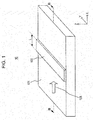
- Fig. 1 is a perspective view illustrating the configuration of a dielectric substrate 10 according to a first embodiment of the present disclosure.
- Fig. 2 is a plan view of the dielectric substrate 10 according to the first embodiment of the present disclosure.
- Fig. 3 is a sectional view, taken along line III-III, of the dielectric substrate 10 illustrated in Fig. 1 .
- the dielectric substrate 10 transmits signals with a frequency f 0 .
- the dielectric substrate 10 has a dielectric 101 and a copper film pattern 102.
- the dielectric substrate 10 may be used, for example, in a radar device.
- the copper film pattern 102 is arranged on an obverse surface (corresponding to a first surface) of the dielectric 101.
- the copper film pattern 102 is also arranged so as to have a first dimension L in a direction parallel to a propagation direction 103 (in Figs. 1 to 3 , in an X-axis direction) of electromagnetic waves that have the frequency f 0 and that propagate on an obverse surface of the dielectric substrate 10.
- the electromagnetic waves with the frequency f 0 are, for example, electromagnetic waves (unwanted radiation) radiated when current flows in an antenna or a transmission line connected to the dielectric substrate 10 (or provided on the dielectric substrate 10).
- ⁇ r represents a relative permittivity of the dielectric 101
- k represents a constant in the range of 0.15 to 0.70
- ⁇ 0 represents a free space wavelength of signals transmitted on the dielectric substrate 10.
- the first dimension L of the copper film pattern 102 is determined by the frequency f 0 of signals transmitted on the dielectric substrate 10 and the relative permittivity ⁇ r of the dielectric 101.
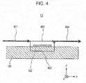
- Fig. 4 illustrates propagation paths when electromagnetic waves that propagate on the obverse surface of the dielectric substrate 10 pass on the copper film pattern 102.
- the electromagnetic waves split to and propagate through a path 402 above the copper film pattern 102 and a path 403 below the copper film pattern 102.
- the electromagnetic waves propagate along one path 404 above the obverse surface of the dielectric substrate 10.
- the present inventors analyzed the amount of attenuation of the electromagnetic waves that propagate on the obverse surface of the dielectric substrate 10 illustrated in Fig. 1 by performing electromagnetic-field simulation using a finite integration method.
- the electromagnetic-field simulation was performed with respect to three types of relative permittivity ( ⁇ r is 2.0, 3.4, and 7.0), assuming three types of actually existing dielectric 101 (polytetrafluoroethylene (PTFE), polyphenylene ether (PPE), and low temperature co-fired ceramic (LTCC)).
- PTFE polytetrafluoroethylene
- PPE polyphenylene ether
- LTCC low temperature co-fired ceramic
- Fig. 5 is a graph illustrating a result of the electromagnetic-field simulation.
- the horizontal axis represents a constant k
- the vertical axis represents the amount of attenuation [dB] of the electromagnetic waves that propagate on the obverse surface of the dielectric substrate 10.
- the reason why the value of k at which the amount of attenuation increases differs depending on the value of the relative permittivity ⁇ r is that the effective value of L differs owing to a fringing effect.
- the copper film pattern 102 having the first dimension L provides an effect of suppressing or reducing the electromagnetic waves in the propagation direction 103.
- the dielectric substrate 10 has the copper film pattern 102 on the obverse surface of the dielectric 101.
- the first dimension L of the copper film pattern 102 in the propagation direction 103 of the electromagnetic waves on the obverse surface of the dielectric substrate 10 is set depending on the frequency f 0 (i.e., the wavelength ⁇ 0 ) of the electromagnetic waves that propagate on the dielectric substrate 10. More specifically, the first dimension L is set so that the phases of electromagnetic waves that propagate along the path 402 above the copper film pattern 102 and the path 403 below the copper film pattern 102 after splitting thereto have opposite phases on the path 404.
- the dielectric substrate 10 makes it possible to suppress or reduce electromagnetic waves that propagate on the obverse surface of the dielectric substrate 10.
- the copper film pattern 102 is provided around an antenna or a transmission line on the dielectric substrate 10 according to the present embodiment, it is possible to suppress or reduce unwanted electromagnetic waves (unwanted radiation) from the antenna or the transmission line.
- the copper film pattern 102 is provided between a plurality of antennas or between a plurality of transmission lines on the dielectric substrate 10 according to the present embodiment, it is possible to improve isolation between the antennas or between the transmission lines.
- the dielectric substrate 10 since the dielectric substrate 10 has the copper film pattern 102 on the obverse surface of the dielectric 101, it is possible to suppress or reduce unwanted electromagnetic waves that propagate on the obverse surface of the dielectric substrate 10. That is, in order to suppress or reduce the electromagnetic waves, the dielectric substrate 10 according to the present embodiment does not need to have an additional member, such as a conductive via as disclosed in Patent Document 1 or a radome as disclosed in Patent Document 2. Accordingly, for example, even when a control circuit or the like is mounted on a reverse surface of the dielectric substrate 10, it is possible to obtain an area for configuring the control circuit or the like. Hence, according to the present embodiment, even when a module including the dielectric substrate 10 is configured, the module can be miniaturized, and there are also an advantage in that the module can be produced at low cost.
- the dielectric substrate 10 makes it possible to suppress or reduce electromagnetic waves that propagate on the obverse surface of the dielectric substrate 10, while avoiding an increase in the structure size.
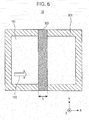
- the dielectric substrate 10 according to the present embodiment may have a configuration in which a ground pattern 601 is provided and a copper film pattern 102 is connected to the ground pattern 601 therearound, as illustrated in Fig. 6 . Even when the dielectric substrate 10 is configured as illustrated in Fig. 6 , advantages that are the same as or similar to the advantages when the dielectric substrate 10 is configurated as illustrated in Fig. 1 are also obtained.
- the copper film pattern 102 on the dielectric substrate 10 according to the present embodiment has a second dimension W in a direction (a Y-axis direction) orthogonal to the electromagnetic-wave propagation direction 103, and the present embodiment is not limited to a case in which the second dimension W is substantially the same as that of the dielectric 101 (e.g., see Fig. 2 ).
- the second dimension W of the copper film pattern 102 may be any dimension that satisfies W>0.5 ⁇ 0 , that is, a condition that the second dimension W is larger than a half wavelength of signals with the frequency f 0 , as illustrated in Fig. 7 .
- a plurality of copper film patterns 102 may be arranged on the obverse surface of the dielectric 101, as illustrated in Fig. 8 .
- a plurality of copper film patterns 102 may be arranged at portions where electromagnetic waves that propagate on the obverse surface of the dielectric 101 concentrate.
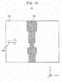
- the first dimension of the copper film pattern 102 in the electromagnetic-wave propagation direction 103 may be ununiform, as illustrated in Fig. 9 or 10 .
- the dielectric substrate 10 can suppress or reduce electromagnetic waves with respect to signals with a different frequency f 0 (the wavelength ⁇ 0 ), in accordance with the range of values taken by the first dimension of the copper film pattern 102 in the electromagnetic-wave propagation direction 103. That is, when the dielectric substrate 10 is configurated as illustrated in Fig. 9 or 10 , it is possible to increase the frequency band in which the effect of suppressing or reducing electromagnetic waves is obtained.
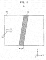
- the copper film pattern 102 is not limited to a pattern that extends in the direction (the Y-axis direction) orthogonal to the electromagnetic-wave propagation direction 103 (the X-axis direction), as illustrated in Fig. 2 , and may be, for example, a pattern that extends obliquely, as illustrated in Fig. 11 .
- Fig. 12 is a perspective view illustrating the configuration of a dielectric substrate 10 according to a second embodiment of the present disclosure.
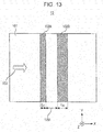
- the dielectric substrate 10 illustrated in Fig. 12 differs from that in the first embodiment (e.g., Fig. 1 ) in that a plurality of copper film patterns 102 (in Fig. 12 , two copper film patterns 102A and 102B) are arranged on an obverse surface of a dielectric 101.
- an arrangement distance 1201 between the copper film patterns 102A and 102B is smaller than or equal to ⁇ 0 .
- the first dimension L in a propagation direction 103 (i.e., in an X-axis direction) of electromagnetic waves on the copper film patterns 102A and 102B satisfies equation (1) noted above.
- the shapes of the copper film patterns 102 do not necessarily have to be the same.
- the value of a first dimension L A of the copper film pattern 102A and the value of a first dimension L B of the copper film pattern 102B in the electromagnetic-wave propagation direction 103 may be different from each other.
- a copper film pattern 102A in which the first dimension in the electromagnetic-wave propagation direction 103 is uniform and a copper film pattern 102B in which the first dimension in the electromagnetic-wave propagation direction 103 is not uniform may be arranged on the obverse surface of the dielectric 101.
- the dielectric substrate 10 makes it possible to increase a frequency band in which the effect of suppressing or reducing electromagnetic waves is obtained.
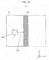
- Fig. 15 is a plan view of a dielectric substrate 10 according to a third embodiment of the present disclosure.
- the dielectric substrate 10 illustrated in Fig. 15 differs from that in the first embodiment (e.g., Fig. 2 ) in that an antenna 1501 is arranged on an obverse surface of a dielectric 101.
- the antenna 1501 radiates signals (radio waves) with a frequency f 0 .
- An arrangement distance 1502 between the antenna 1501 and a copper film pattern 102 i.e., an arrangement distance in an X-axis direction in Fig. 15 ) is smaller than or equal to 2 ⁇ 0 .
- the antenna 1501 may be arranged between adjacent copper film patterns 102, as illustrated in Fig. 16 . With this arrangement, unwanted radiation emitted from the antenna 1501 can be suppressed or reduced in both positive and negative X-axis directions.
- the antenna 1501 arranged on the dielectric 101 according to the present embodiment is not limited to the configuration illustrated in Fig. 15 .
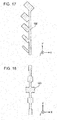
- the antenna 1501 may have a shape, for example, as illustrated in Fig. 17, 18 , or 19 , as long as it is formed of a copper film.
- Fig. 20 is a plan view of a dielectric substrate 10 according to a fourth embodiment of the present disclosure.
- the dielectric substrate 10 illustrated in Fig. 20 differs from that in the third embodiment (e.g., Fig. 15 ) in that a transmission line 2001 is arranged on an obverse surface of a dielectric 101.
- the transmission line 2001 transmits signals with a frequency f 0 .
- An arrangement distance 2002 between the transmission line 2001 and a copper film pattern 102 i.e., an arrangement distance in an X-axis direction in Fig. 20 ) is smaller than or equal to 2 ⁇ 0 .
- the copper film pattern 102 can suppress or reduce unwanted radiation emitted from the transmission line 2001 in the X-axis direction in Fig. 20 (the X-axis direction corresponds to the electromagnetic-wave propagation direction 103 in Fig. 2 ).
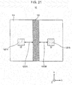
- Fig. 21 is a plan view of a dielectric substrate 10 according to a fifth embodiment of the present disclosure.
- the dielectric substrate 10 illustrated in Fig. 21 differs from that in the third embodiment (e.g., Fig. 15 ) in that, on an obverse surface of a dielectric 101, antennas 1501A and 1501 B are arranged in X-axis positive and negative directions of a copper film pattern 102, and the copper film pattern 102 is arranged between the antennas 1501 A and 1501 B.
- an arrangement distance 1502A between the antenna 1501A and the copper film pattern 102 is smaller than or equal to 2 ⁇ 0 (where ⁇ 0 represents a free space wavelength of signals radiated from the antenna 1501A).
- ⁇ 0 represents a free space wavelength of signals radiated from the antenna 1501A.
- the antenna 1501A may be used as a receiving antenna, and the antenna 1501B may be used as a transmitting antenna.
- an arrangement distance 1502B may be set according to a free space wavelength of signals radiated from the antenna 1501 B, as in the case in which the antenna 1501A is used as a transmitting antenna, and the antenna 1501B is used as a receiving antenna.
- a plurality of copper film patterns 102 may be arranged between the antenna 1501 A and the antenna 1501B, as illustrated in Fig. 22 . With this arrangement, it is possible to enhance the isolation-improving effect provided by the copper film patterns 102.
- Fig. 23 is a plan view of a dielectric substrate 10 according to a sixth embodiment of the present disclosure.
- the dielectric substrate 10 in Fig. 23 differs from that in the fifth embodiment (e.g., Fig. 21 ) in that transmission lines 2001 A and 2001 B are arranged on a dielectric 101, and a copper film pattern 102 is arranged between the transmission lines 2001A and 2001B.
- An arrangement distance 2002A between the transmission line 2001A and the copper film pattern 102 i.e., an arrangement distance in an X-axis direction in Fig. 23
- An arrangement distance 2002B between the transmission line 2001 B and the copper film pattern 102 i.e., an arrangement distance in the X-axis direction in Fig. 23
- the copper film pattern 102 is provided between the transmission lines 2001A and 2001 B, and different signals are transmitted through the transmission lines 2001A and 2001B, it is possible to suppress or reduce unwanted radiation emitted from each of the transmission lines 2001A and 2001B. and it is possible to reduce crosstalk noise.
- a first dimension L of the copper film pattern 102 in an X-axis direction is determined by the frequency f 0 of signals transmitted through the transmission line 2001A or 2001B (e.g., see equation (1)).
- the copper film pattern 102 when the copper film pattern 102 is provided between the transmission lines 2001A and 2001 B, signals with a frequency f 0 are transmitted through the transmission line 2001A, and signals with a frequency f 1 are transmitted through the transmission line 2001 B, the copper film pattern 102 can suppress or reduce unwanted radiation emitted from the transmission line 2001 A.
- a plurality of copper film patterns 102 may be arranged between the transmission lines 2001 A and 2001 B, as in Fig. 24 . With this arrangement, it is possible to enhance the crosstalk-noise reducing effect provided by the copper film pattern 102.
- the present disclosure can be realized by software, hardware, or software in cooperation with hardware.
- Each functional block used in the description of each embodiment described above can be partly or entirely realized by an LSI such as an integrated circuit, and each process described in each embodiment may be controlled partly or entirely by the same LSI or a combination of LSIs.
- the LSI may be individually formed as chips, or one chip may be formed so as to include a part or all of the functional blocks.
- the LSI may include a data input and output coupled thereto.
- the LSI here may be referred to as an IC, a system LSI, a super LSI, or an ultra LSI depending on a difference in the degree of integration.
- the technique of implementing an integrated circuit is not limited to the LSI and may be realized by using a dedicated circuit, a general-purpose processor, or a special-purpose processor.
- a field programmable gate array FPGA
- FPGA field programmable gate array
- the present disclosure can be realized as digital processing or analogue processing.
- One aspect of the present disclosure can be applied to a dielectric substrate that transmits signals with a frequency f 0 and that suppresses or reduces electromagnetic waves that propagate on an obverse surface of a dielectric substrate.
Landscapes
- Variable-Direction Aerials And Aerial Arrays (AREA)
- Details Of Aerials (AREA)
- Radar Systems Or Details Thereof (AREA)
- Aerials With Secondary Devices (AREA)
Abstract

Description
- The present disclosure relates to a dielectric substrate and an antenna device.
- When current flows in a conductor, electromagnetic waves are radiated. In particular, when current flows in an antenna or a transmission line on a dielectric substrate, unintended electromagnetic waves are radiated (unwanted radiation) and propagate on an obverse surface of the dielectric substrate, which may cause generation of null in antenna directivity or may cause interference, which is crosstalk noise.
- Japanese Unexamined Patent Application Publication (Translation of PCT Application) No.
2002-510886 2012-93305 Patent Document 2") discloses a technology in which a radome with an upright wall that provides shielding between a transmitting antenna and a receiving antenna formed on a dielectric to thereby suppress or reduce electromagnetic waves that propagate on an obverse surface of a dielectric substrate from the transmitting antenna to the receiving antenna. - However, in Patent Document 1, the conductive vias need to be arranged on the obverse surface of the dielectric substrate, and thus, when a control circuit or the like is mounted on a reverse surface of the dielectric substrate, the arranged conductive vias limit an area where the control circuit or the like can be configured, and when an antenna device is configured as a module including a dielectric substrate and a control circuit, the module size may increase. Also, in
Patent Document 2, it is necessary to add the radome in addition to the dielectric substrate, the structure size increases, and the cost increases. - One non-limiting and exemplary embodiment facilitates providing a dielectric substrate and an antenna device that can suppress or reduce electromagnetic waves that propagate on a dielectric substrate, while avoiding an increase in the structure size.
- In one general aspect, the techniques disclosed here feature a dielectric substrate for transmitting a signal with a frequency f0. The dielectric substrate includes a dielectric and a copper film pattern arranged on a first surface of the dielectric. The copper film pattern has a first dimension L in a direction parallel to a propagation direction of an electromagnetic wave that has the frequency f0 and that propagates on the first surface, and the first dimension L is given by:

- According to the present disclosure, it is possible to suppress or reduce electromagnetic waves that propagate on a dielectric substrate, while avoiding an increase in the structure size.
- Additional benefits and advantages of the disclosed embodiments will become apparent from the specification and drawings. The benefits and/or advantages may be individually obtained by the various embodiments and features of the specification and drawings, which need not all be provided in order to obtain one or more of such benefits and/or advantages.
-
-
Fig. 1 is a perspective view illustrating a dielectric substrate according to a first embodiment; -
Fig. 2 is a plan view illustrating the dielectric substrate according to the first embodiment; -
Fig. 3 is a transverse sectional view illustrating the dielectric substrate according to the first embodiment; -
Fig. 4 is a view illustrating paths through which electromagnetic waves propagate along the dielectric substrate according to the first embodiment; -
Fig. 5 is a graph illustrating a result of electromagnetic-field simulation that analyzes the amount of attenuation of electromagnetic waves that propagate on the dielectric substrate according to the first embodiment; -
Fig. 6 is a plan view illustrating another example of the dielectric substrate according to the first embodiment; -
Fig. 7 is a plan view illustrating another example of the dielectric substrate according to the first embodiment; -
Fig. 8 is a plan view illustrating another example of the dielectric substrate according to the first embodiment; -
Fig. 9 is a plan view illustrating another example of the dielectric substrate according to the first embodiment; -
Fig. 10 is a plan view illustrating another example of the dielectric substrate according to the first embodiment; -
Fig. 11 is a plan view illustrating another example of the dielectric substrate according to the first embodiment; -
Fig. 12 is a perspective view illustrating a dielectric substrate according to a second embodiment; -
Fig. 13 is a plan view illustrating another example of the dielectric substrate according to the second embodiment; -
Fig. 14 is a plan view illustrating another example of the dielectric substrate according to the second embodiment; -
Fig. 15 is a plan view illustrating one example of a dielectric substrate according to a third embodiment; -
Fig. 16 is a plan view illustrating another example of the dielectric substrate according to the third embodiment; -
Fig. 17 is a view illustrating one example of an antenna according to the third embodiment; -
Fig. 18 is a view illustrating another example of the antenna according to the third embodiment; -
Fig. 19 is a view illustrating another example of the antenna according to the third embodiment; -
Fig. 20 is a plan view illustrating one example of a dielectric substrate according to a fourth embodiment; -
Fig. 21 is a plan view illustrating one example of a dielectric substrate according to a fifth embodiment; -
Fig. 22 is a plan view illustrating another example of the dielectric substrate according to the fifth embodiment; -
Fig. 23 is a plan view illustrating one example of a dielectric substrate according to a sixth embodiment; and -
Fig. 24 is a plan view illustrating another example of the dielectric substrate according to the sixth embodiment. - Embodiments of the present disclosure will be described below in detail with reference to the accompanying drawings. Each of the embodiments described below is an example, and the present disclosure is not limited to the embodiments. In the following description, the same or similar constituent elements are denoted by the same reference numerals.
-
Fig. 1 is a perspective view illustrating the configuration of adielectric substrate 10 according to a first embodiment of the present disclosure.Fig. 2 is a plan view of thedielectric substrate 10 according to the first embodiment of the present disclosure.Fig. 3 is a sectional view, taken along line III-III, of thedielectric substrate 10 illustrated inFig. 1 . - The
dielectric substrate 10 according to the present embodiment transmits signals with a frequency f0. Thedielectric substrate 10 has a dielectric 101 and acopper film pattern 102. Thedielectric substrate 10 may be used, for example, in a radar device. - As illustrated in
Fig. 1 , thecopper film pattern 102 is arranged on an obverse surface (corresponding to a first surface) of the dielectric 101. Thecopper film pattern 102 is also arranged so as to have a first dimension L in a direction parallel to a propagation direction 103 (inFigs. 1 to 3 , in an X-axis direction) of electromagnetic waves that have the frequency f0 and that propagate on an obverse surface of thedielectric substrate 10. The electromagnetic waves with the frequency f0 are, for example, electromagnetic waves (unwanted radiation) radiated when current flows in an antenna or a transmission line connected to the dielectric substrate 10 (or provided on the dielectric substrate 10). - The first dimension L of the
copper film pattern 102 is given by:
- In equation (1), εr represents a relative permittivity of the dielectric 101, k represents a constant in the range of 0.15 to 0.70, and λ0 represents a free space wavelength of signals transmitted on the
dielectric substrate 10. - That is, in the present embodiment, the first dimension L of the
copper film pattern 102 is determined by the frequency f0 of signals transmitted on thedielectric substrate 10 and the relative permittivity εr of the dielectric 101. -
Fig. 4 illustrates propagation paths when electromagnetic waves that propagate on the obverse surface of thedielectric substrate 10 pass on thecopper film pattern 102. As illustrated inFig. 4 , when electromagnetic waves that propagate along one path 401 on the obverse surface of thedielectric substrate 10 pass on thecopper film pattern 102, the electromagnetic waves split to and propagate through apath 402 above thecopper film pattern 102 and apath 403 below thecopper film pattern 102. After the electromagnetic waves pass on thecopper film pattern 102, the electromagnetic waves propagate along onepath 404 above the obverse surface of thedielectric substrate 10. - In this case, when the first dimension L of the
copper film pattern 102 in the electromagnetic-wave propagation direction 103 is set to the value in equation (1), electromagnetic waves that have propagated along therespective paths respective paths path 404, the electromagnetic waves that have propagated along therespective paths dielectric substrate 10 attenuate on thepath 404. As a result, the electromagnetic waves that propagate on the dielectric 101 are suppressed or reduced by thecopper film pattern 102. - The present inventors analyzed the amount of attenuation of the electromagnetic waves that propagate on the obverse surface of the
dielectric substrate 10 illustrated inFig. 1 by performing electromagnetic-field simulation using a finite integration method. The electromagnetic-field simulation was performed with respect to three types of relative permittivity (εr is 2.0, 3.4, and 7.0), assuming three types of actually existing dielectric 101 (polytetrafluoroethylene (PTFE), polyphenylene ether (PPE), and low temperature co-fired ceramic (LTCC)). -
Fig. 5 is a graph illustrating a result of the electromagnetic-field simulation. InFig. 5 , the horizontal axis represents a constant k, and the vertical axis represents the amount of attenuation [dB] of the electromagnetic waves that propagate on the obverse surface of thedielectric substrate 10. In addition, inFig. 5 , a characteristic 501 represents a characteristic of the amount of attenuation for the relative permittivity εr = 2.0, a characteristic 502 represents a characteristic of the amount of attenuation for the relative permittivity εr = 3.4, and a characteristic 503 represents a characteristic of the amount of attenuation for the relative permittivity εr = 7.0. -
Fig. 5 shows that, in the range of k = 0.15 to 0.70, the amount of attenuation of the electromagnetic waves that propagate on the obverse surface of thedielectric substrate 10 increases. The reason why the value of k at which the amount of attenuation increases differs depending on the value of the relative permittivity εr is that the effective value of L differs owing to a fringing effect. - Also, in the electromagnetic-field simulation result illustrated in
Fig. 5 , in the range of k = 0.15 to 0.70, for example, in the vicinity of k = 0.3, the effect of increasing the amount of attenuation decreases. This is because the analysis in the electromagnetic-field simulation is performed using only three types of relative permittivity (i.e., εr is 2.0, 3.4, and 7.0) by way of example, and in the range of the relative permittivity εr = 2.0 to 7.0, other relative permittivities at which the amount of attenuation increases, for example, in the vicinity of k = 0.3 exist. In other words, k = 0.15 and k = 0.7 are the minimum value and the maximum value, respectively, of the constant k at which thecopper film pattern 102 can provide an effect of increasing the amount of attenuation of the electromagnetic waves, and a characteristic in which the amount of attenuation of the electromagnetic waves increases in the range of k = 0.15 to 0.70 according to the relative permittivity εr of the dielectric 101 is obtained. - In addition,
Fig. 5 also illustrates an effect of increasing the amount of attenuation outside the range of k = 0.15 to 0.70, and this effect is due to the arrangement of thecopper film pattern 102. - Thus, it can be understood from
Fig. 5 that, in the range of k = 0.15 to 0.70, thecopper film pattern 102 having the first dimension L provides an effect of suppressing or reducing the electromagnetic waves in thepropagation direction 103. - As described above, in the present embodiment, the
dielectric substrate 10 has thecopper film pattern 102 on the obverse surface of the dielectric 101. Also, in accordance with equation (1), the first dimension L of thecopper film pattern 102 in thepropagation direction 103 of the electromagnetic waves on the obverse surface of thedielectric substrate 10 is set depending on the frequency f0 (i.e., the wavelength λ0) of the electromagnetic waves that propagate on thedielectric substrate 10. More specifically, the first dimension L is set so that the phases of electromagnetic waves that propagate along thepath 402 above thecopper film pattern 102 and thepath 403 below thecopper film pattern 102 after splitting thereto have opposite phases on thepath 404. - With this arrangement, the
dielectric substrate 10 makes it possible to suppress or reduce electromagnetic waves that propagate on the obverse surface of thedielectric substrate 10. Hence, for example, when thecopper film pattern 102 is provided around an antenna or a transmission line on thedielectric substrate 10 according to the present embodiment, it is possible to suppress or reduce unwanted electromagnetic waves (unwanted radiation) from the antenna or the transmission line. Alternatively, when thecopper film pattern 102 is provided between a plurality of antennas or between a plurality of transmission lines on thedielectric substrate 10 according to the present embodiment, it is possible to improve isolation between the antennas or between the transmission lines. - Also, according to the present embodiment, since the
dielectric substrate 10 has thecopper film pattern 102 on the obverse surface of the dielectric 101, it is possible to suppress or reduce unwanted electromagnetic waves that propagate on the obverse surface of thedielectric substrate 10. That is, in order to suppress or reduce the electromagnetic waves, thedielectric substrate 10 according to the present embodiment does not need to have an additional member, such as a conductive via as disclosed in Patent Document 1 or a radome as disclosed inPatent Document 2. Accordingly, for example, even when a control circuit or the like is mounted on a reverse surface of thedielectric substrate 10, it is possible to obtain an area for configuring the control circuit or the like. Hence, according to the present embodiment, even when a module including thedielectric substrate 10 is configured, the module can be miniaturized, and there are also an advantage in that the module can be produced at low cost. - Thus, according to the present embodiment, the
dielectric substrate 10 makes it possible to suppress or reduce electromagnetic waves that propagate on the obverse surface of thedielectric substrate 10, while avoiding an increase in the structure size. - The
dielectric substrate 10 according to the present embodiment may have a configuration in which aground pattern 601 is provided and acopper film pattern 102 is connected to theground pattern 601 therearound, as illustrated inFig. 6 . Even when thedielectric substrate 10 is configured as illustrated inFig. 6 , advantages that are the same as or similar to the advantages when thedielectric substrate 10 is configurated as illustrated inFig. 1 are also obtained. - In addition, the
copper film pattern 102 on thedielectric substrate 10 according to the present embodiment has a second dimension W in a direction (a Y-axis direction) orthogonal to the electromagnetic-wave propagation direction 103, and the present embodiment is not limited to a case in which the second dimension W is substantially the same as that of the dielectric 101 (e.g., seeFig. 2 ). For example, the second dimension W of thecopper film pattern 102 may be any dimension that satisfies W>0.5λ0, that is, a condition that the second dimension W is larger than a half wavelength of signals with the frequency f0, as illustrated inFig. 7 . - In addition, in the
dielectric substrate 10 according to the present embodiment, a plurality ofcopper film patterns 102 may be arranged on the obverse surface of the dielectric 101, as illustrated inFig. 8 . For example, a plurality ofcopper film patterns 102 may be arranged at portions where electromagnetic waves that propagate on the obverse surface of the dielectric 101 concentrate. InFig. 8 , it is sufficient that the second dimension W of eachcopper film pattern 102 in the Y-axis direction satisfies W>0.5λ0, as in the case inFig. 7 . - Also, in the
dielectric substrate 10 according to the present embodiment, the first dimension of thecopper film pattern 102 in the electromagnetic-wave propagation direction 103 may be ununiform, as illustrated inFig. 9 or10 . With such an arrangement, thedielectric substrate 10 can suppress or reduce electromagnetic waves with respect to signals with a different frequency f0 (the wavelength λ0), in accordance with the range of values taken by the first dimension of thecopper film pattern 102 in the electromagnetic-wave propagation direction 103. That is, when thedielectric substrate 10 is configurated as illustrated inFig. 9 or10 , it is possible to increase the frequency band in which the effect of suppressing or reducing electromagnetic waves is obtained. - Also, in the
dielectric substrate 10 according to the present embodiment, thecopper film pattern 102 is not limited to a pattern that extends in the direction (the Y-axis direction) orthogonal to the electromagnetic-wave propagation direction 103 (the X-axis direction), as illustrated inFig. 2 , and may be, for example, a pattern that extends obliquely, as illustrated inFig. 11 . -
Fig. 12 is a perspective view illustrating the configuration of adielectric substrate 10 according to a second embodiment of the present disclosure. - The
dielectric substrate 10 illustrated inFig. 12 differs from that in the first embodiment (e.g.,Fig. 1 ) in that a plurality of copper film patterns 102 (inFig. 12 , twocopper film patterns - Also, in the electromagnetic-
wave propagation direction 103, anarrangement distance 1201 between thecopper film patterns copper film patterns - With this configuration, since electromagnetic waves can be suppressed or reduced in each of the
copper film patterns 102 arranged on the obverse surface of the dielectric 101, the effect of suppressing or reducing electromagnetic waves that propagate on the obverse surface of thedielectric substrate 10 can be more enhanced than that in the first embodiment. - The shapes of the
copper film patterns 102 do not necessarily have to be the same. For example, as illustrated inFig. 13 , the value of a first dimension LA of thecopper film pattern 102A and the value of a first dimension LB of thecopper film pattern 102B in the electromagnetic-wave propagation direction 103 may be different from each other. Alternatively, as illustrated inFig. 14 , acopper film pattern 102A in which the first dimension in the electromagnetic-wave propagation direction 103 is uniform and acopper film pattern 102B in which the first dimension in the electromagnetic-wave propagation direction 103 is not uniform may be arranged on the obverse surface of the dielectric 101. With this arrangement, electromagnetic waves with a plurality of frequencies can be suppressed or reduced in accordance with the first dimensions of thecopper film patterns 102 inpropagation directions 103 of the respective electromagnetic waves. That is, thedielectric substrate 10 makes it possible to increase a frequency band in which the effect of suppressing or reducing electromagnetic waves is obtained. -
Fig. 15 is a plan view of adielectric substrate 10 according to a third embodiment of the present disclosure. - The
dielectric substrate 10 illustrated inFig. 15 differs from that in the first embodiment (e.g.,Fig. 2 ) in that anantenna 1501 is arranged on an obverse surface of a dielectric 101. - The
antenna 1501 radiates signals (radio waves) with a frequency f0. Anarrangement distance 1502 between theantenna 1501 and a copper film pattern 102 (i.e., an arrangement distance in an X-axis direction inFig. 15 ) is smaller than or equal to 2λ0. - With this configuration, when the
copper film pattern 102 is provided on the obverse surface of the dielectric 101, unwanted radiation emitted from theantenna 1501 can be suppressed or reduced in the X-axis direction inFig. 15 (the X-axis direction corresponds to the electromagnetic-wave propagation direction 103 inFig. 2 ). - In the
dielectric substrate 10 according to the present embodiment, for example, theantenna 1501 may be arranged between adjacentcopper film patterns 102, as illustrated inFig. 16 . With this arrangement, unwanted radiation emitted from theantenna 1501 can be suppressed or reduced in both positive and negative X-axis directions. - Also, the
antenna 1501 arranged on the dielectric 101 according to the present embodiment is not limited to the configuration illustrated inFig. 15 . Theantenna 1501 may have a shape, for example, as illustrated inFig. 17, 18 , or19 , as long as it is formed of a copper film. -
Fig. 20 is a plan view of adielectric substrate 10 according to a fourth embodiment of the present disclosure. - The
dielectric substrate 10 illustrated inFig. 20 differs from that in the third embodiment (e.g.,Fig. 15 ) in that atransmission line 2001 is arranged on an obverse surface of a dielectric 101. - The
transmission line 2001 transmits signals with a frequency f0. Anarrangement distance 2002 between thetransmission line 2001 and a copper film pattern 102 (i.e., an arrangement distance in an X-axis direction inFig. 20 ) is smaller than or equal to 2λ0. - With this configuration, the
copper film pattern 102 can suppress or reduce unwanted radiation emitted from thetransmission line 2001 in the X-axis direction inFig. 20 (the X-axis direction corresponds to the electromagnetic-wave propagation direction 103 inFig. 2 ). -
Fig. 21 is a plan view of adielectric substrate 10 according to a fifth embodiment of the present disclosure. - The
dielectric substrate 10 illustrated inFig. 21 differs from that in the third embodiment (e.g.,Fig. 15 ) in that, on an obverse surface of a dielectric 101,antennas copper film pattern 102, and thecopper film pattern 102 is arranged between theantennas - The following description will be given of an example in which the
antenna 1501A is a transmitting antenna and theantenna 1501 B is a receiving antenna. In this, in the X-axis direction inFig. 21 , anarrangement distance 1502A between theantenna 1501A and thecopper film pattern 102 is smaller than or equal to 2λ0 (where λ0 represents a free space wavelength of signals radiated from theantenna 1501A). With this arrangement, thecopper film pattern 102 can suppress or reduce unwanted radiation emitted from theantenna 1501 A, thus making it possible to improve isolation. Theantenna 1501A may be used as a receiving antenna, and theantenna 1501B may be used as a transmitting antenna. When theantenna 1501 A is used as a receiving antenna, and theantenna 1501 B is used as a transmitting antenna, anarrangement distance 1502B may be set according to a free space wavelength of signals radiated from theantenna 1501 B, as in the case in which theantenna 1501A is used as a transmitting antenna, and theantenna 1501B is used as a receiving antenna. - In the present embodiment, a plurality of
copper film patterns 102 may be arranged between theantenna 1501 A and theantenna 1501B, as illustrated inFig. 22 . With this arrangement, it is possible to enhance the isolation-improving effect provided by thecopper film patterns 102. -
Fig. 23 is a plan view of adielectric substrate 10 according to a sixth embodiment of the present disclosure. - The
dielectric substrate 10 inFig. 23 differs from that in the fifth embodiment (e.g.,Fig. 21 ) in thattransmission lines copper film pattern 102 is arranged between thetransmission lines arrangement distance 2002A between thetransmission line 2001A and the copper film pattern 102 (i.e., an arrangement distance in an X-axis direction inFig. 23 ) may be smaller than or equal to 2λ0, as inFig. 20 . Anarrangement distance 2002B between thetransmission line 2001 B and the copper film pattern 102 (i.e., an arrangement distance in the X-axis direction inFig. 23 ) may be smaller than or equal to 2λ0, as inFig. 20 . - For example, when the
copper film pattern 102 is provided between thetransmission lines transmission lines transmission lines 2001A and 2001B. and it is possible to reduce crosstalk noise. - In this case, a first dimension L of the
copper film pattern 102 in an X-axis direction is determined by the frequency f0 of signals transmitted through thetransmission line copper film pattern 102 is provided between thetransmission lines transmission line 2001A, and signals with a frequency f1 are transmitted through thetransmission line 2001 B, thecopper film pattern 102 can suppress or reduce unwanted radiation emitted from thetransmission line 2001 A. - In the present embodiment, a plurality of
copper film patterns 102 may be arranged between thetransmission lines Fig. 24 . With this arrangement, it is possible to enhance the crosstalk-noise reducing effect provided by thecopper film pattern 102. - The present disclosure can be realized by software, hardware, or software in cooperation with hardware.
- Each functional block used in the description of each embodiment described above can be partly or entirely realized by an LSI such as an integrated circuit, and each process described in each embodiment may be controlled partly or entirely by the same LSI or a combination of LSIs. The LSI may be individually formed as chips, or one chip may be formed so as to include a part or all of the functional blocks. The LSI may include a data input and output coupled thereto. The LSI here may be referred to as an IC, a system LSI, a super LSI, or an ultra LSI depending on a difference in the degree of integration.
- However, the technique of implementing an integrated circuit is not limited to the LSI and may be realized by using a dedicated circuit, a general-purpose processor, or a special-purpose processor. In addition, a field programmable gate array (FPGA) that can be programmed after the manufacture of the LSI or a reconfigurable processor in which the connections and the settings of circuit cells arranged inside the LSI can be reconfigured may be used. The present disclosure can be realized as digital processing or analogue processing.
- If future integrated circuit technology replaces LSIs as a result of the advancement of semiconductor technology or other derivative technology, the functional blocks could be integrated using the future integrated circuit technology. Biotechnology can also be applied.
- One aspect of the present disclosure can be applied to a dielectric substrate that transmits signals with a frequency f0 and that suppresses or reduces electromagnetic waves that propagate on an obverse surface of a dielectric substrate.
Claims (10)
- A dielectric substrate for transmitting a signal with a frequency f0, the dielectric substrate comprising:a dielectric; anda copper film pattern arranged on a first surface of the dielectric,wherein the copper film pattern has a first dimension L in a direction parallel to a propagation direction of an electromagnetic wave that has the frequency f0 and that propagates on the first surface, and the first dimension L is given by:

- The dielectric substrate according to claim 1,
wherein the copper film pattern arranged on the first surface comprises a plurality of copper film patterns, and
in the propagation direction of the electromagnetic wave, a distance between adjacent copper film patterns of the plurality of copper film patterns is smaller than or equal to λ0. - The dielectric substrate according to claim 1,
wherein an antenna that radiates the signal with the frequency f0 is arranged on the first surface, and
in the propagation direction of the electromagnetic wave, a distance between the antenna and the copper film pattern is smaller than or equal to 2λ0. - The dielectric substrate according to claim 3,
wherein the antenna arranged on the first surface comprises a plurality of antennas, and
the copper film pattern is arranged between the antennas. - The dielectric substrate according to claim 4,
wherein the dielectric substrate is used in a radar device. - The dielectric substrate according to claim 1,
wherein a transmission line for transmitting the signal with the frequency f0 is arranged on the first surface, and
in the propagation direction of the electromagnetic wave, a distance between the transmission line and the copper film pattern is smaller than or equal to 2λ0. - The dielectric substrate according to claim 6,
wherein the transmission line arranged on the first surface comprises a plurality of transmission lines, and
the copper film pattern is arranged between the transmission lines. - The dielectric substrate according to claim 6,
wherein the dielectric substrate is used in a radar device. - The dielectric substrate according to claim 1,
wherein the copper film pattern has a second dimension in a direction orthogonal to the propagation direction of the electromagnetic wave that propagates on the first surface, and the second dimension is larger than λ0/2. - An antenna device comprising:an antenna that radiates signal with a frequency f0; anda dielectric substrate for transmitting the signal, the dielectric substrate having a dielectric and a copper film pattern arranged on a first surface of the dielectric,wherein the copper film pattern has a first dimension L in a direction parallel to a propagation direction of an electromagnetic wave that has the frequency f0 and that propagates on the first surface, and the first dimension L is given by:

Applications Claiming Priority (1)
| Application Number | Priority Date | Filing Date | Title |
|---|---|---|---|
| JP2016109197A JP6704169B2 (en) | 2016-05-31 | 2016-05-31 | Dielectric substrate and antenna device |
Publications (2)
| Publication Number | Publication Date |
|---|---|
| EP3252869A1 true EP3252869A1 (en) | 2017-12-06 |
| EP3252869B1 EP3252869B1 (en) | 2020-04-22 |
Family
ID=58745142
Family Applications (1)
| Application Number | Title | Priority Date | Filing Date |
|---|---|---|---|
| EP17172170.7A Active EP3252869B1 (en) | 2016-05-31 | 2017-05-22 | Dielectric substrate and antenna device |
Country Status (4)
| Country | Link |
|---|---|
| US (1) | US10396452B2 (en) |
| EP (1) | EP3252869B1 (en) |
| JP (1) | JP6704169B2 (en) |
| CN (1) | CN107437655B (en) |
Families Citing this family (5)
| Publication number | Priority date | Publication date | Assignee | Title |
|---|---|---|---|---|
| JP6954376B2 (en) * | 2017-12-28 | 2021-10-27 | 株式会社村田製作所 | Antenna array and antenna module |
| WO2020066453A1 (en) * | 2018-09-27 | 2020-04-02 | 株式会社村田製作所 | Antenna device and communication device |
| WO2021153035A1 (en) * | 2020-01-30 | 2021-08-05 | 株式会社村田製作所 | Antenna device |
| US20230199702A1 (en) * | 2021-12-21 | 2023-06-22 | Kerstin Johnsson | Wifi architecture for proximate sensing |
| CN120073312A (en) * | 2023-11-29 | 2025-05-30 | 深圳富泰宏精密工业有限公司 | Array antenna module and wireless communication device |
Citations (6)
| Publication number | Priority date | Publication date | Assignee | Title |
|---|---|---|---|---|
| US5898405A (en) * | 1994-12-27 | 1999-04-27 | Kabushiki Kaisha Toshiba | Omnidirectional antenna formed one or two antenna elements symmetrically to a ground conductor |
| US6218989B1 (en) * | 1994-12-28 | 2001-04-17 | Lucent Technologies, Inc. | Miniature multi-branch patch antenna |
| JP2002510886A (en) | 1998-03-30 | 2002-04-09 | ザ リージェンツ オブ ザ ユニバーシテイ オブ カリフォルニア | Circuit and method for removing metal surface current |
| JP2012093305A (en) | 2010-10-28 | 2012-05-17 | Denso Corp | Radar device and radome |
| WO2016013790A1 (en) * | 2014-07-22 | 2016-01-28 | 엘지이노텍 주식회사 | Radar apparatus |
| US20160134021A1 (en) * | 2014-11-06 | 2016-05-12 | Sony Corporation | Stripline coupled antenna with periodic slots for wireless electronic devices |
Family Cites Families (21)
| Publication number | Priority date | Publication date | Assignee | Title |
|---|---|---|---|---|
| JP3734671B2 (en) * | 2000-03-31 | 2006-01-11 | 三菱電機株式会社 | Antenna device |
| US6795021B2 (en) * | 2002-03-01 | 2004-09-21 | Massachusetts Institute Of Technology | Tunable multi-band antenna array |
| GB0302326D0 (en) * | 2003-02-01 | 2003-03-05 | Qinetiq Ltd | Phased array antenna and inter-element mutual coupling control method |
| JP2005094440A (en) * | 2003-09-18 | 2005-04-07 | Tdk Corp | Antenna system and radar system |
| KR100859864B1 (en) * | 2005-06-13 | 2008-09-24 | 삼성전자주식회사 | Flat Panel Array Antenna with Isolation Element |
| KR100706024B1 (en) * | 2005-10-19 | 2007-04-12 | 한국전자통신연구원 | Millimeter wave band wideband microstrip-waveguide converter |
| CN1979945A (en) * | 2005-11-30 | 2007-06-13 | 微星科技股份有限公司 | Configuration structure of the same frequency band antenna on the circuit board |
| US7629930B2 (en) * | 2006-10-20 | 2009-12-08 | Hong Kong Applied Science And Technology Research Institute Co., Ltd. | Systems and methods using ground plane filters for device isolation |
| JP2008300897A (en) * | 2007-05-29 | 2008-12-11 | Ngk Spark Plug Co Ltd | Antenna unit |
| JP5294443B2 (en) * | 2007-06-21 | 2013-09-18 | 三星電子株式会社 | Antenna device and wireless communication terminal |
| JP4966125B2 (en) * | 2007-07-27 | 2012-07-04 | 株式会社東芝 | Antenna device and radio |
| JP5041416B2 (en) * | 2007-11-12 | 2012-10-03 | 日本無線株式会社 | Antenna device |
| TW200935659A (en) * | 2008-02-04 | 2009-08-16 | Pegatron Corp | Dual-feed planar antenna |
| US8780002B2 (en) * | 2010-07-15 | 2014-07-15 | Sony Corporation | Multiple-input multiple-output (MIMO) multi-band antennas with a conductive neutralization line for signal decoupling |
| CN102104193B (en) * | 2010-12-01 | 2015-04-01 | 中兴通讯股份有限公司 | Multiple input multiple output antenna system |
| CN202111211U (en) * | 2011-03-08 | 2012-01-11 | 东莞宇龙通信科技有限公司 | A bluetooth antenna, bluetooth device and mobile communication terminal |
| FR2994342B1 (en) * | 2012-07-31 | 2016-02-05 | Eads Europ Aeronautic Defence | DEVICE FOR DECOUPLING BETWEEN ANTENNAS - IN PARTICULAR PATCH ANTENNAS MOUNTED ON AN AIRCRAFT |
| JP6047795B2 (en) * | 2012-11-12 | 2016-12-21 | 日東電工株式会社 | Antenna module |
| CN104218317A (en) * | 2013-06-03 | 2014-12-17 | 中兴通讯股份有限公司 | Printed circuit board and wireless terminal adopting multiple-input multiple-output antenna technology |
| CN104577330B (en) * | 2013-10-09 | 2018-02-13 | 国基电子(上海)有限公司 | Multi-input/output antenna |
| CN104979635B (en) * | 2014-04-03 | 2018-07-24 | 中国移动通信集团公司 | A kind of array antenna |
-
2016
- 2016-05-31 JP JP2016109197A patent/JP6704169B2/en not_active Expired - Fee Related
-
2017
- 2017-04-25 CN CN201710275312.7A patent/CN107437655B/en active Active
- 2017-05-22 EP EP17172170.7A patent/EP3252869B1/en active Active
- 2017-05-23 US US15/602,147 patent/US10396452B2/en active Active
Patent Citations (6)
| Publication number | Priority date | Publication date | Assignee | Title |
|---|---|---|---|---|
| US5898405A (en) * | 1994-12-27 | 1999-04-27 | Kabushiki Kaisha Toshiba | Omnidirectional antenna formed one or two antenna elements symmetrically to a ground conductor |
| US6218989B1 (en) * | 1994-12-28 | 2001-04-17 | Lucent Technologies, Inc. | Miniature multi-branch patch antenna |
| JP2002510886A (en) | 1998-03-30 | 2002-04-09 | ザ リージェンツ オブ ザ ユニバーシテイ オブ カリフォルニア | Circuit and method for removing metal surface current |
| JP2012093305A (en) | 2010-10-28 | 2012-05-17 | Denso Corp | Radar device and radome |
| WO2016013790A1 (en) * | 2014-07-22 | 2016-01-28 | 엘지이노텍 주식회사 | Radar apparatus |
| US20160134021A1 (en) * | 2014-11-06 | 2016-05-12 | Sony Corporation | Stripline coupled antenna with periodic slots for wireless electronic devices |
Non-Patent Citations (1)
| Title |
|---|
| LEI WANG ET AL: "Wideband High-Gain 60-GHz LTCC L-Probe Patch Antenna Array With a Soft Surface", IEEE TRANSACTIONS ON ANTENNAS AND PROPAGATION, IEEE SERVICE CENTER, PISCATAWAY, NJ, US, vol. 61, no. 4, 1 April 2013 (2013-04-01), pages 1802 - 1809, XP011499213, ISSN: 0018-926X, DOI: 10.1109/TAP.2012.2220331 * |
Also Published As
| Publication number | Publication date |
|---|---|
| JP6704169B2 (en) | 2020-06-03 |
| JP2017216587A (en) | 2017-12-07 |
| US10396452B2 (en) | 2019-08-27 |
| US20170346180A1 (en) | 2017-11-30 |
| CN107437655B (en) | 2021-01-12 |
| CN107437655A (en) | 2017-12-05 |
| EP3252869B1 (en) | 2020-04-22 |
Similar Documents
| Publication | Publication Date | Title |
|---|---|---|
| US10396452B2 (en) | Dielectric substrate and antenna device | |
| KR101621480B1 (en) | Transit structure of waveguide and dielectric waveguide | |
| WO2016112839A1 (en) | Combination antenna element, array and printed circuit board | |
| US20180277946A1 (en) | Antenna apparatus | |
| JP2022523001A (en) | Antenna device with integrated filter with laminated planar resonator | |
| JP2016220029A (en) | Antenna device, radio communication device and radar device | |
| CA2689154A1 (en) | Impedance-controlled coplanar waveguide system for the three-dimensional distribution of high-bandwidth signals | |
| CN104488365B (en) | The circuit board of high-frequency unit equipped with transmitting interference wave | |
| CN113767526B (en) | Multi-feed slot antenna | |
| EP3379905B1 (en) | Circuit board | |
| US20160003934A1 (en) | Stacked waveguide substrate, radio communication module, and radar system | |
| CN113767523A (en) | Front shielding, coplanar waveguide, direct-feed type and back cavity type slot antenna | |
| AU2013239324B2 (en) | Enhanced connected tiled array antenna | |
| EP3968450B1 (en) | Wireless communication module | |
| US20100182103A1 (en) | Interconnection apparatus and method for low cross-talk chip mounting for automotive radars | |
| KR102059329B1 (en) | Ultra wideband dipole antenna | |
| CN115411480B (en) | A radio frequency structure, detection device and communication system | |
| Athanasopoulos et al. | Design and Development of 60 GHz Millimeter-wave Passive Components using Substrate Integrated Waveguide Technology | |
| Athanasopoulos et al. | Millimeter-wave passive front-end based on substrate integrated waveguide technology | |
| Belen et al. | Modeling and realization of cavity-backed dual band SIW antenna | |
| RU2802170C1 (en) | Ebg cells and antenna array containing ebg cells | |
| JP6184610B2 (en) | High-frequency device and method for manufacturing high-frequency device | |
| US11575189B1 (en) | Multi-layer bandpass filter | |
| Elkarkraoui et al. | Terahertz Band Interconnect Architecture for Future Chip-to-Chip Wireless Communication | |
| US20240413529A1 (en) | Fourth order orbital angular momentum (oam) mode patch antenna |
Legal Events
| Date | Code | Title | Description |
|---|---|---|---|
| PUAI | Public reference made under article 153(3) epc to a published international application that has entered the european phase |
Free format text: ORIGINAL CODE: 0009012 |
|
| STAA | Information on the status of an ep patent application or granted ep patent |
Free format text: STATUS: THE APPLICATION HAS BEEN PUBLISHED |
|
| AK | Designated contracting states |
Kind code of ref document: A1 Designated state(s): AL AT BE BG CH CY CZ DE DK EE ES FI FR GB GR HR HU IE IS IT LI LT LU LV MC MK MT NL NO PL PT RO RS SE SI SK SM TR |
|
| AX | Request for extension of the european patent |
Extension state: BA ME |
|
| STAA | Information on the status of an ep patent application or granted ep patent |
Free format text: STATUS: REQUEST FOR EXAMINATION WAS MADE |
|
| 17P | Request for examination filed |
Effective date: 20180427 |
|
| RBV | Designated contracting states (corrected) |
Designated state(s): AL AT BE BG CH CY CZ DE DK EE ES FI FR GB GR HR HU IE IS IT LI LT LU LV MC MK MT NL NO PL PT RO RS SE SI SK SM TR |
|
| STAA | Information on the status of an ep patent application or granted ep patent |
Free format text: STATUS: EXAMINATION IS IN PROGRESS |
|
| 17Q | First examination report despatched |
Effective date: 20180803 |
|
| 17Q | First examination report despatched |
Effective date: 20180817 |
|
| GRAP | Despatch of communication of intention to grant a patent |
Free format text: ORIGINAL CODE: EPIDOSNIGR1 |
|
| STAA | Information on the status of an ep patent application or granted ep patent |
Free format text: STATUS: GRANT OF PATENT IS INTENDED |
|
| RIC1 | Information provided on ipc code assigned before grant |
Ipc: H01Q 9/04 20060101ALN20191115BHEP Ipc: H01Q 1/52 20060101AFI20191115BHEP Ipc: H01Q 21/00 20060101ALN20191115BHEP |
|
| RIC1 | Information provided on ipc code assigned before grant |
Ipc: H01Q 9/04 20060101ALN20191122BHEP Ipc: H01Q 21/00 20060101ALN20191122BHEP Ipc: H01Q 1/52 20060101AFI20191122BHEP |
|
| INTG | Intention to grant announced |
Effective date: 20191209 |
|
| GRAS | Grant fee paid |
Free format text: ORIGINAL CODE: EPIDOSNIGR3 |
|
| GRAA | (expected) grant |
Free format text: ORIGINAL CODE: 0009210 |
|
| STAA | Information on the status of an ep patent application or granted ep patent |
Free format text: STATUS: THE PATENT HAS BEEN GRANTED |
|
| AK | Designated contracting states |
Kind code of ref document: B1 Designated state(s): AL AT BE BG CH CY CZ DE DK EE ES FI FR GB GR HR HU IE IS IT LI LT LU LV MC MK MT NL NO PL PT RO RS SE SI SK SM TR |
|
| REG | Reference to a national code |
Ref country code: CH Ref legal event code: EP |
|
| REG | Reference to a national code |
Ref country code: IE Ref legal event code: FG4D |
|
| REG | Reference to a national code |
Ref country code: DE Ref legal event code: R096 Ref document number: 602017015035 Country of ref document: DE |
|
| REG | Reference to a national code |
Ref country code: AT Ref legal event code: REF Ref document number: 1261367 Country of ref document: AT Kind code of ref document: T Effective date: 20200515 |
|
| REG | Reference to a national code |
Ref country code: LT Ref legal event code: MG4D |
|
| REG | Reference to a national code |
Ref country code: NL Ref legal event code: MP Effective date: 20200422 |
|
| PG25 | Lapsed in a contracting state [announced via postgrant information from national office to epo] |
Ref country code: NO Free format text: LAPSE BECAUSE OF FAILURE TO SUBMIT A TRANSLATION OF THE DESCRIPTION OR TO PAY THE FEE WITHIN THE PRESCRIBED TIME-LIMIT Effective date: 20200722 Ref country code: GR Free format text: LAPSE BECAUSE OF FAILURE TO SUBMIT A TRANSLATION OF THE DESCRIPTION OR TO PAY THE FEE WITHIN THE PRESCRIBED TIME-LIMIT Effective date: 20200723 Ref country code: PT Free format text: LAPSE BECAUSE OF FAILURE TO SUBMIT A TRANSLATION OF THE DESCRIPTION OR TO PAY THE FEE WITHIN THE PRESCRIBED TIME-LIMIT Effective date: 20200824 Ref country code: LT Free format text: LAPSE BECAUSE OF FAILURE TO SUBMIT A TRANSLATION OF THE DESCRIPTION OR TO PAY THE FEE WITHIN THE PRESCRIBED TIME-LIMIT Effective date: 20200422 Ref country code: FI Free format text: LAPSE BECAUSE OF FAILURE TO SUBMIT A TRANSLATION OF THE DESCRIPTION OR TO PAY THE FEE WITHIN THE PRESCRIBED TIME-LIMIT Effective date: 20200422 Ref country code: IS Free format text: LAPSE BECAUSE OF FAILURE TO SUBMIT A TRANSLATION OF THE DESCRIPTION OR TO PAY THE FEE WITHIN THE PRESCRIBED TIME-LIMIT Effective date: 20200822 Ref country code: SE Free format text: LAPSE BECAUSE OF FAILURE TO SUBMIT A TRANSLATION OF THE DESCRIPTION OR TO PAY THE FEE WITHIN THE PRESCRIBED TIME-LIMIT Effective date: 20200422 Ref country code: NL Free format text: LAPSE BECAUSE OF FAILURE TO SUBMIT A TRANSLATION OF THE DESCRIPTION OR TO PAY THE FEE WITHIN THE PRESCRIBED TIME-LIMIT Effective date: 20200422 |
|
| REG | Reference to a national code |
Ref country code: AT Ref legal event code: MK05 Ref document number: 1261367 Country of ref document: AT Kind code of ref document: T Effective date: 20200422 |
|
| PG25 | Lapsed in a contracting state [announced via postgrant information from national office to epo] |
Ref country code: RS Free format text: LAPSE BECAUSE OF FAILURE TO SUBMIT A TRANSLATION OF THE DESCRIPTION OR TO PAY THE FEE WITHIN THE PRESCRIBED TIME-LIMIT Effective date: 20200422 Ref country code: LV Free format text: LAPSE BECAUSE OF FAILURE TO SUBMIT A TRANSLATION OF THE DESCRIPTION OR TO PAY THE FEE WITHIN THE PRESCRIBED TIME-LIMIT Effective date: 20200422 Ref country code: HR Free format text: LAPSE BECAUSE OF FAILURE TO SUBMIT A TRANSLATION OF THE DESCRIPTION OR TO PAY THE FEE WITHIN THE PRESCRIBED TIME-LIMIT Effective date: 20200422 Ref country code: BG Free format text: LAPSE BECAUSE OF FAILURE TO SUBMIT A TRANSLATION OF THE DESCRIPTION OR TO PAY THE FEE WITHIN THE PRESCRIBED TIME-LIMIT Effective date: 20200722 |
|
| PG25 | Lapsed in a contracting state [announced via postgrant information from national office to epo] |
Ref country code: AL Free format text: LAPSE BECAUSE OF FAILURE TO SUBMIT A TRANSLATION OF THE DESCRIPTION OR TO PAY THE FEE WITHIN THE PRESCRIBED TIME-LIMIT Effective date: 20200422 |
|
| REG | Reference to a national code |
Ref country code: DE Ref legal event code: R097 Ref document number: 602017015035 Country of ref document: DE |
|
| PG25 | Lapsed in a contracting state [announced via postgrant information from national office to epo] |
Ref country code: ES Free format text: LAPSE BECAUSE OF FAILURE TO SUBMIT A TRANSLATION OF THE DESCRIPTION OR TO PAY THE FEE WITHIN THE PRESCRIBED TIME-LIMIT Effective date: 20200422 Ref country code: MC Free format text: LAPSE BECAUSE OF FAILURE TO SUBMIT A TRANSLATION OF THE DESCRIPTION OR TO PAY THE FEE WITHIN THE PRESCRIBED TIME-LIMIT Effective date: 20200422 Ref country code: LI Free format text: LAPSE BECAUSE OF NON-PAYMENT OF DUE FEES Effective date: 20200531 Ref country code: CH Free format text: LAPSE BECAUSE OF NON-PAYMENT OF DUE FEES Effective date: 20200531 Ref country code: CZ Free format text: LAPSE BECAUSE OF FAILURE TO SUBMIT A TRANSLATION OF THE DESCRIPTION OR TO PAY THE FEE WITHIN THE PRESCRIBED TIME-LIMIT Effective date: 20200422 Ref country code: DK Free format text: LAPSE BECAUSE OF FAILURE TO SUBMIT A TRANSLATION OF THE DESCRIPTION OR TO PAY THE FEE WITHIN THE PRESCRIBED TIME-LIMIT Effective date: 20200422 Ref country code: AT Free format text: LAPSE BECAUSE OF FAILURE TO SUBMIT A TRANSLATION OF THE DESCRIPTION OR TO PAY THE FEE WITHIN THE PRESCRIBED TIME-LIMIT Effective date: 20200422 Ref country code: RO Free format text: LAPSE BECAUSE OF FAILURE TO SUBMIT A TRANSLATION OF THE DESCRIPTION OR TO PAY THE FEE WITHIN THE PRESCRIBED TIME-LIMIT Effective date: 20200422 Ref country code: IT Free format text: LAPSE BECAUSE OF FAILURE TO SUBMIT A TRANSLATION OF THE DESCRIPTION OR TO PAY THE FEE WITHIN THE PRESCRIBED TIME-LIMIT Effective date: 20200422 Ref country code: SM Free format text: LAPSE BECAUSE OF FAILURE TO SUBMIT A TRANSLATION OF THE DESCRIPTION OR TO PAY THE FEE WITHIN THE PRESCRIBED TIME-LIMIT Effective date: 20200422 Ref country code: EE Free format text: LAPSE BECAUSE OF FAILURE TO SUBMIT A TRANSLATION OF THE DESCRIPTION OR TO PAY THE FEE WITHIN THE PRESCRIBED TIME-LIMIT Effective date: 20200422 |
|
| PG25 | Lapsed in a contracting state [announced via postgrant information from national office to epo] |
Ref country code: PL Free format text: LAPSE BECAUSE OF FAILURE TO SUBMIT A TRANSLATION OF THE DESCRIPTION OR TO PAY THE FEE WITHIN THE PRESCRIBED TIME-LIMIT Effective date: 20200422 Ref country code: SK Free format text: LAPSE BECAUSE OF FAILURE TO SUBMIT A TRANSLATION OF THE DESCRIPTION OR TO PAY THE FEE WITHIN THE PRESCRIBED TIME-LIMIT Effective date: 20200422 |
|
| PLBE | No opposition filed within time limit |
Free format text: ORIGINAL CODE: 0009261 |
|
| STAA | Information on the status of an ep patent application or granted ep patent |
Free format text: STATUS: NO OPPOSITION FILED WITHIN TIME LIMIT |
|
| REG | Reference to a national code |
Ref country code: BE Ref legal event code: MM Effective date: 20200531 |
|
| 26N | No opposition filed |
Effective date: 20210125 |
|
| PG25 | Lapsed in a contracting state [announced via postgrant information from national office to epo] |
Ref country code: LU Free format text: LAPSE BECAUSE OF NON-PAYMENT OF DUE FEES Effective date: 20200522 |
|
| PG25 | Lapsed in a contracting state [announced via postgrant information from national office to epo] |
Ref country code: IE Free format text: LAPSE BECAUSE OF NON-PAYMENT OF DUE FEES Effective date: 20200522 Ref country code: FR Free format text: LAPSE BECAUSE OF NON-PAYMENT OF DUE FEES Effective date: 20200622 |
|
| PG25 | Lapsed in a contracting state [announced via postgrant information from national office to epo] |
Ref country code: SI Free format text: LAPSE BECAUSE OF FAILURE TO SUBMIT A TRANSLATION OF THE DESCRIPTION OR TO PAY THE FEE WITHIN THE PRESCRIBED TIME-LIMIT Effective date: 20200422 Ref country code: BE Free format text: LAPSE BECAUSE OF NON-PAYMENT OF DUE FEES Effective date: 20200531 |
|
| GBPC | Gb: european patent ceased through non-payment of renewal fee |
Effective date: 20210522 |
|
| PG25 | Lapsed in a contracting state [announced via postgrant information from national office to epo] |
Ref country code: GB Free format text: LAPSE BECAUSE OF NON-PAYMENT OF DUE FEES Effective date: 20210522 |
|
| PG25 | Lapsed in a contracting state [announced via postgrant information from national office to epo] |
Ref country code: TR Free format text: LAPSE BECAUSE OF FAILURE TO SUBMIT A TRANSLATION OF THE DESCRIPTION OR TO PAY THE FEE WITHIN THE PRESCRIBED TIME-LIMIT Effective date: 20200422 Ref country code: MT Free format text: LAPSE BECAUSE OF FAILURE TO SUBMIT A TRANSLATION OF THE DESCRIPTION OR TO PAY THE FEE WITHIN THE PRESCRIBED TIME-LIMIT Effective date: 20200422 Ref country code: CY Free format text: LAPSE BECAUSE OF FAILURE TO SUBMIT A TRANSLATION OF THE DESCRIPTION OR TO PAY THE FEE WITHIN THE PRESCRIBED TIME-LIMIT Effective date: 20200422 |
|
| PG25 | Lapsed in a contracting state [announced via postgrant information from national office to epo] |
Ref country code: MK Free format text: LAPSE BECAUSE OF FAILURE TO SUBMIT A TRANSLATION OF THE DESCRIPTION OR TO PAY THE FEE WITHIN THE PRESCRIBED TIME-LIMIT Effective date: 20200422 |
|
| REG | Reference to a national code |
Ref country code: DE Ref legal event code: R081 Ref document number: 602017015035 Country of ref document: DE Owner name: PANASONIC AUTOMOTIVE SYSTEMS CO., LTD., YOKOHA, JP Free format text: FORMER OWNER: PANASONIC INTELLECTUAL PROPERTY MANAGEMENT CO., LTD., OSAKA-SHI, JP |
|
| PGFP | Annual fee paid to national office [announced via postgrant information from national office to epo] |
Ref country code: DE Payment date: 20250521 Year of fee payment: 9 |