EP3252867A1 - Terminal - Google Patents
Terminal Download PDFInfo
- Publication number
- EP3252867A1 EP3252867A1 EP15886838.0A EP15886838A EP3252867A1 EP 3252867 A1 EP3252867 A1 EP 3252867A1 EP 15886838 A EP15886838 A EP 15886838A EP 3252867 A1 EP3252867 A1 EP 3252867A1
- Authority
- EP
- European Patent Office
- Prior art keywords
- ground point
- point
- terminal
- ground
- signal feed
- Prior art date
- Legal status (The legal status is an assumption and is not a legal conclusion. Google has not performed a legal analysis and makes no representation as to the accuracy of the status listed.)
- Granted
Links
Images



Classifications
-
- H—ELECTRICITY
- H01—ELECTRIC ELEMENTS
- H01Q—ANTENNAS, i.e. RADIO AERIALS
- H01Q5/00—Arrangements for simultaneous operation of antennas on two or more different wavebands, e.g. dual-band or multi-band arrangements
- H01Q5/30—Arrangements for providing operation on different wavebands
- H01Q5/307—Individual or coupled radiating elements, each element being fed in an unspecified way
- H01Q5/314—Individual or coupled radiating elements, each element being fed in an unspecified way using frequency dependent circuits or components, e.g. trap circuits or capacitors
- H01Q5/328—Individual or coupled radiating elements, each element being fed in an unspecified way using frequency dependent circuits or components, e.g. trap circuits or capacitors between a radiating element and ground
-
- H—ELECTRICITY
- H01—ELECTRIC ELEMENTS
- H01Q—ANTENNAS, i.e. RADIO AERIALS
- H01Q1/00—Details of, or arrangements associated with, antennas
- H01Q1/44—Details of, or arrangements associated with, antennas using equipment having another main function to serve additionally as an antenna, e.g. means for giving an antenna an aesthetic aspect
-
- H—ELECTRICITY
- H01—ELECTRIC ELEMENTS
- H01Q—ANTENNAS, i.e. RADIO AERIALS
- H01Q1/00—Details of, or arrangements associated with, antennas
- H01Q1/12—Supports; Mounting means
- H01Q1/22—Supports; Mounting means by structural association with other equipment or articles
- H01Q1/24—Supports; Mounting means by structural association with other equipment or articles with receiving set
- H01Q1/241—Supports; Mounting means by structural association with other equipment or articles with receiving set used in mobile communications, e.g. GSM
- H01Q1/242—Supports; Mounting means by structural association with other equipment or articles with receiving set used in mobile communications, e.g. GSM specially adapted for hand-held use
- H01Q1/243—Supports; Mounting means by structural association with other equipment or articles with receiving set used in mobile communications, e.g. GSM specially adapted for hand-held use with built-in antennas
-
- H—ELECTRICITY
- H01—ELECTRIC ELEMENTS
- H01Q—ANTENNAS, i.e. RADIO AERIALS
- H01Q13/00—Waveguide horns or mouths; Slot antennas; Leaky-waveguide antennas; Equivalent structures causing radiation along the transmission path of a guided wave
- H01Q13/10—Resonant slot antennas
- H01Q13/106—Microstrip slot antennas
-
- H—ELECTRICITY
- H01—ELECTRIC ELEMENTS
- H01Q—ANTENNAS, i.e. RADIO AERIALS
- H01Q21/00—Antenna arrays or systems
- H01Q21/28—Combinations of substantially independent non-interacting antenna units or systems
-
- H—ELECTRICITY
- H01—ELECTRIC ELEMENTS
- H01Q—ANTENNAS, i.e. RADIO AERIALS
- H01Q5/00—Arrangements for simultaneous operation of antennas on two or more different wavebands, e.g. dual-band or multi-band arrangements
- H01Q5/30—Arrangements for providing operation on different wavebands
- H01Q5/307—Individual or coupled radiating elements, each element being fed in an unspecified way
- H01Q5/314—Individual or coupled radiating elements, each element being fed in an unspecified way using frequency dependent circuits or components, e.g. trap circuits or capacitors
- H01Q5/335—Individual or coupled radiating elements, each element being fed in an unspecified way using frequency dependent circuits or components, e.g. trap circuits or capacitors at the feed, e.g. for impedance matching
-
- H—ELECTRICITY
- H01—ELECTRIC ELEMENTS
- H01Q—ANTENNAS, i.e. RADIO AERIALS
- H01Q9/00—Electrically-short antennas having dimensions not more than twice the operating wavelength and consisting of conductive active radiating elements
- H01Q9/04—Resonant antennas
- H01Q9/0407—Substantially flat resonant element parallel to ground plane, e.g. patch antenna
- H01Q9/0421—Substantially flat resonant element parallel to ground plane, e.g. patch antenna with a shorting wall or a shorting pin at one end of the element
-
- H—ELECTRICITY
- H04—ELECTRIC COMMUNICATION TECHNIQUE
- H04B—TRANSMISSION
- H04B1/00—Details of transmission systems, not covered by a single one of groups H04B3/00 - H04B13/00; Details of transmission systems not characterised by the medium used for transmission
- H04B1/38—Transceivers, i.e. devices in which transmitter and receiver form a structural unit and in which at least one part is used for functions of transmitting and receiving
- H04B1/3827—Portable transceivers
- H04B1/3888—Arrangements for carrying or protecting transceivers
-
- H—ELECTRICITY
- H04—ELECTRIC COMMUNICATION TECHNIQUE
- H04M—TELEPHONIC COMMUNICATION
- H04M1/00—Substation equipment, e.g. for use by subscribers
- H04M1/02—Constructional features of telephone sets
- H04M1/0202—Portable telephone sets, e.g. cordless phones, mobile phones or bar type handsets
- H04M1/026—Details of the structure or mounting of specific components
Definitions
- the present invention relates to the field of communications technologies, and in particular, to a terminal.
- a terminal on a mobile communications network sends and receives a signal by using a terminal antenna.
- bandwidth of the terminal antenna needs to cover more frequency bands, that is, the terminal antenna needs to have more resonance points.
- an antenna of a terminal with a metal back cover can generate a relatively small quantity of resonance points, and bandwidth of the terminal antenna is relatively narrow.
- Embodiments of the present invention provide a terminal, so as to extend bandwidth of a terminal antenna.
- a terminal is provided.
- a metal back cover of the terminal has a slot, the slot divides the metal back cover into two parts, and one of the two parts is used as an antenna radiator of the terminal.
- the antenna radiator has a signal feed point, a first ground point, and at least one second ground point, so that an antenna of the terminal has four resonance points.
- the signal feed point is connected to a matching network, the first ground point is grounded by using a switch device, and the second ground point is grounded.
- a distance between the signal feed point and the first ground point is less than a distance between the signal feed point and the second ground point, and none of the signal feed point, the first ground point, and the second ground point is located in a position, corresponding to an end of the slot, on the antenna radiator.
- the second ground point of the antenna radiator is specifically grounded by using an adjustable device.
- the second ground point of the antenna radiator is specifically grounded by using a fixed capacitor and/or a fixed inductor.
- the antenna radiator further has a third ground point, the third ground point is grounded, and the third ground point is located in the position, corresponding to the end of the slot, on the antenna radiator.
- the third ground point of the antenna radiator is specifically grounded by using an adjustable device.
- the third ground point of the antenna radiator is specifically grounded by using a fixed capacitor and/or a fixed inductor.
- the first ground point of the antenna radiator is specifically grounded by using an inductor and/or a capacitor, and the switch device.
- the matching network connected to the signal feed point of the antenna radiator is specifically a variable capacitor.
- a metal back cover of the terminal has a slot, the slot divides the metal back cover into two parts, one of the two parts is used as an antenna radiator of the terminal, and the antenna radiator has a signal feed point, a first ground point that is relatively close to the signal feed point, and a second ground point that is relatively distant from the signal feed point; and the signal feed point is connected to a matching network, the first ground point is grounded by using a switch device, the second ground point is grounded, and none of the signal feed point, the first ground point, and the second ground point is located in a position, corresponding to an end of the slot, on the antenna radiator.
- the terminal antenna With use of the terminal provided by the embodiments of the present invention, no matter whether a terminal antenna is in a low-frequency or high-frequency operating state, the terminal antenna can have totally four resonance points: one resonance point in a left-handed mode and three resonance points in a slot mode. Compared with the prior art, bandwidth of the terminal antenna is wider.
- embodiments of the present invention provide a terminal.
- the following describes the embodiments of the present invention with reference to the accompanying drawings in the specification. It should be understood that the preferred embodiments described herein are merely for describing and explaining the present invention, but are not intended to limit the present invention. Moreover, the embodiments in this application and the features in the embodiments can be mutually combined when no conflict is caused.
- An embodiment of the present invention provides a terminal.
- a metal back cover of the terminal has a slot 100.
- the slot 100 divides the metal back cover into two parts. One of the two parts is used as an antenna radiator 101 of the terminal, and the other one is used as a main ground part 102.
- the antenna radiator 101 has a signal feed point F, a first ground point G1, and at least one second ground point G2, so that an antenna of the terminal has four resonance points.
- the signal feed point F is connected to a matching network, the first ground point G1 is grounded by using a switch device, and the second ground point G2 is grounded.
- a distance between the signal feed point F and the first ground point G1 is less than a distance between the signal feed point F and the second ground point G2, and none of the signal feed point F, the first ground point G1, and the second ground point G2 is located in a position, corresponding to an end of the slot 100, on the antenna radiator 101.
- the end of the slot 100 is a position in which the slot 100 and a side frame of the terminal are connected.
- the second ground point G2 of the antenna radiator 101 may be directly grounded.
- the second ground point G2 of the antenna radiator 101 may be directly grounded by being directly connected to a printed circuit board of the terminal, or the second ground point G2 of the antenna radiator may be directly grounded by being directly connected to the main ground part 102. That is, as shown in FIG. 2 , there may be no connection point between the two parts of the metal back cover of the terminal; or as shown in FIG. 3 , there may be a connection point in the slot 100 and in a position, corresponding to the second ground point G2, of the antenna radiator 101.
- the second ground point G2 of the antenna radiator 101 may also be grounded by using a fixed capacitor and/or a fixed inductor.
- the second ground point G2 is grounded by using an LC filter formed by a fixed capacitor and a fixed inductor.
- the second ground point G2 of the antenna radiator 101 may also be grounded by using an adjustable device.
- the second ground point G2 is grounded by using a variable capacitor or a switch device, so that a resonance coverage area can be enlarged.
- the antenna radiator 101 may have a third ground point G3 in addition to the signal feed point F, the first ground point G1, and the second ground point G2, and the third ground point G3 is grounded. Moreover, the third ground point G3 is located in the position, corresponding to the end of the slot 100, on the antenna radiator 101.
- the third ground point G3 of the antenna radiator 101 may be directly grounded.
- the third ground point G3 of the antenna radiator 101 may be directly grounded by being directly connected to the printed circuit board of the terminal, or the third ground point G3 of the antenna radiator may be directly grounded by being directly connected to the main ground part 102. That is, as shown in FIG. 7 , there may be a connection point between the two parts of the metal back cover of the terminal at the end of the slot 100 and in a position, corresponding to the third ground point G3, of the antenna radiator 101.
- the third ground point G3 of the antenna radiator 101 may also be grounded by using a fixed capacitor and/or a fixed inductor, for example, grounded by using an LC filter formed by a fixed capacitor and a fixed inductor.
- the third ground point G3 of the antenna radiator 101 may also be grounded by using an adjustable device, for example, grounded by using a variable capacitor or a switch device. This is not illustrated or described in detail herein.
- an inductor and a capacitor may be connected into a ground branch of the first ground point G1 of the antenna radiator 101, that is, the first ground point G1 may be specifically grounded by using the inductor and/or the capacitor, and the switch device.
- the switch device may be specifically a double-pole double-throw DPDT switch.
- the switch device in the ground branch of the first ground point G1 may be specifically the double-pole double-throw DPDT switch shown in FIG. 8 , or may be a single-pole single-throw SPST switch, a single-pole double-throw SPDT switch, a single-pole four-throw SP4T switch, or the like. This is not specifically limited by the present invention.
- the terminal antenna When the switch device in the ground branch of the first ground point G1 of the antenna radiator 101 is off and the first ground point G1 is in an open circuit, the terminal antenna is in a low-frequency operating state. When the switch device in the ground branch of the first ground point G1 of the antenna radiator 101 is on and the first ground point G1 is short-circuited to ground, the terminal antenna is in a high-frequency operating state. That is, an operating status of the terminal antenna can be controlled by controlling a status of the switch device in the ground branch of the first ground point G1 of the antenna radiator 101.
- the matching network connected to the signal feed point F of the antenna radiator 101 includes a capacitor, and may further include an inductor.
- the matching network may be a variable capacitor, so as to facilitate impedance matching.
- a terminal provided by Embodiment 1 of the present invention is shown in FIG. 9 .
- An antenna radiator 101 has a signal feed point F, a first ground point G1, and two second ground points G21 and G22.
- the signal feed point F is connected to a variable capacitor
- the first ground point G1 is grounded by using a double-pole double-throw DPDT switch
- the two second ground points G21 and G22 are both directly grounded.
- the first ground point G1 may be grounded by being connected to a printed circuit board of the terminal by using the double-pole double-throw DPDT switch.
- the second ground point G21 may be grounded by being connected to the printed circuit board of the terminal.
- the second ground point G22 of a terminal antenna may be grounded by being connected to a main ground part 102 of the metal back cover of the terminal by using a mechanical part.
- the terminal antenna When the double-pole double-throw DPDT switch in a ground branch of the first ground point G1 of the antenna radiator 101 is off and the first ground point G1 is in an open circuit, the terminal antenna is in a low-frequency operating state.
- the signal feed point F and the two second ground points G21 and G22 are short-circuit points, two ends of the slot 100 are open-circuit points, and the following resonances may be formed in the terminal antenna:
- the terminal antenna has one resonance point in the left-handed mode and three resonance points in the slot mode.
- the terminal antenna When the double-pole double-throw DPDT switch in the ground branch of the first ground point G1 of the antenna radiator 101 is on and the first ground point G1 is short-circuited to ground, the terminal antenna is in a high-frequency operating state.
- the signal feed point F, the first ground point G1, and the two second ground points G21 and G22 are all short-circuit points, the two ends of the slot 100 are open-circuit points, and the following resonances may be formed in the terminal antenna:
- the terminal antenna in the high-frequency operating state, can also have one resonance point in the left-handed mode and three resonance points in the slot mode.
- specific positions of the signal feed point F, the first ground point G1, and the two second ground points G21 and G22 of the antenna radiator 101 may be set according to a requirement of an actual application scenario.
- the terminal antenna can achieve 1710 MHz - 2700 MHz full-band coverage.
- a terminal provided by Embodiment 2 of the present invention is shown in FIG. 10 .
- a difference lies in that there is a connection point that is between the two parts of the metal back cover of the terminal and that is at the left end of the slot 100. Due to existence of the connection point, this is equivalent to that the antenna radiator 101 has an additional third ground point G3 that is directly grounded.
- a resonance in a slot mode that is formed between the left end of the slot 100 and the second ground point G22 corresponds to 1/2 of a guided-wave wavelength.
- a ground point that is grounded by using an adjustable device may be further added between the left end of the slot 100 and the second ground point G22, and an electrical length between the left end of the slot 100 and the second ground point G22 can be changed, so as to adjust the resonance in the slot mode and change a resonance frequency.
- the terminal antenna can have four resonance points: one resonance point in a left-handed mode and three resonance points in a slot mode. Compared with the prior art, bandwidth of the terminal antenna can be extended, and performance of the terminal antenna can be improved.
Landscapes
- Engineering & Computer Science (AREA)
- Computer Networks & Wireless Communication (AREA)
- Waveguide Aerials (AREA)
- Details Of Aerials (AREA)
- Support Of Aerials (AREA)
Abstract
Description
- The present invention relates to the field of communications technologies, and in particular, to a terminal.
- A terminal on a mobile communications network sends and receives a signal by using a terminal antenna. With technical development and application, bandwidth of the terminal antenna needs to cover more frequency bands, that is, the terminal antenna needs to have more resonance points.
- However, in pursuit of aesthetics, increasing metal materials are added to an exterior of the terminal, such as an all-metal back cover. For the antenna, the metal materials severely affect the bandwidth, worsen performance, and cause difficulty in design of the terminal antenna. In the prior art, whether in a low-frequency or high-frequency operating state, an antenna of a terminal with a metal back cover can generate a relatively small quantity of resonance points, and bandwidth of the terminal antenna is relatively narrow.
- Embodiments of the present invention provide a terminal, so as to extend bandwidth of a terminal antenna.
- According to a first aspect, a terminal is provided. A metal back cover of the terminal has a slot, the slot divides the metal back cover into two parts, and one of the two parts is used as an antenna radiator of the terminal. The antenna radiator has a signal feed point, a first ground point, and at least one second ground point, so that an antenna of the terminal has four resonance points.
- The signal feed point is connected to a matching network, the first ground point is grounded by using a switch device, and the second ground point is grounded. A distance between the signal feed point and the first ground point is less than a distance between the signal feed point and the second ground point, and none of the signal feed point, the first ground point, and the second ground point is located in a position, corresponding to an end of the slot, on the antenna radiator.
- With reference to the first aspect, in a first possible implementation manner, the second ground point of the antenna radiator is specifically grounded by using an adjustable device.
- With reference to the first aspect, in a second possible implementation manner, the second ground point of the antenna radiator is specifically grounded by using a fixed capacitor and/or a fixed inductor.
- With reference to the first aspect, the first possible implementation manner of the first aspect, or the second possible implementation manner of the first aspect, in a third possible implementation manner, the antenna radiator further has a third ground point, the third ground point is grounded, and the third ground point is located in the position, corresponding to the end of the slot, on the antenna radiator.
- With reference to the third possible implementation manner of the first aspect, in a fourth possible implementation manner, the third ground point of the antenna radiator is specifically grounded by using an adjustable device.
- With reference to the third possible implementation manner of the first aspect, in a fifth possible implementation manner, the third ground point of the antenna radiator is specifically grounded by using a fixed capacitor and/or a fixed inductor.
- With reference to the first aspect, the second possible implementation manner of the first aspect, the third possible implementation manner of the first aspect, the fourth possible implementation manner of the first aspect, or the fifth possible implementation manner of the first aspect, in a sixth possible implementation manner, the first ground point of the antenna radiator is specifically grounded by using an inductor and/or a capacitor, and the switch device.
- With reference to the first aspect, the second possible implementation manner of the first aspect, the third possible implementation manner of the first aspect, the fourth possible implementation manner of the first aspect, the fifth possible implementation manner of the first aspect, or the sixth possible implementation manner of the first aspect, in a seventh possible implementation manner, the matching network connected to the signal feed point of the antenna radiator is specifically a variable capacitor.
- According to the terminal provided by the first aspect, a metal back cover of the terminal has a slot, the slot divides the metal back cover into two parts, one of the two parts is used as an antenna radiator of the terminal, and the antenna radiator has a signal feed point, a first ground point that is relatively close to the signal feed point, and a second ground point that is relatively distant from the signal feed point; and the signal feed point is connected to a matching network, the first ground point is grounded by using a switch device, the second ground point is grounded, and none of the signal feed point, the first ground point, and the second ground point is located in a position, corresponding to an end of the slot, on the antenna radiator. With use of the terminal provided by the embodiments of the present invention, no matter whether a terminal antenna is in a low-frequency or high-frequency operating state, the terminal antenna can have totally four resonance points: one resonance point in a left-handed mode and three resonance points in a slot mode. Compared with the prior art, bandwidth of the terminal antenna is wider.
- The drawings are provided to further understand the present invention, and they constitute a part of the application. The drawings, along with the embodiments of the present invention, are used to explain the present invention, and pose no limitation on the present invention. In the drawings:
-
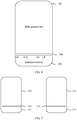
FIG. 1 is a first schematic diagram of a terminal according to an embodiment of the present invention; -
FIG. 2 is a first schematic diagram of a metal back cover of a terminal according to an embodiment of the present invention; -
FIG. 3 is a second schematic diagram of a metal back cover of a terminal according to an embodiment of the present invention; -
FIG. 4 is a first schematic diagram of a second ground point of a terminal antenna according to an embodiment of the present invention; -
FIG. 5 is a second schematic diagram of a second ground point of a terminal antenna according to an embodiment of the present invention; -
FIG. 6 is a second schematic diagram of a terminal according to an embodiment of the present invention; -
FIG. 7 is a third schematic diagram of a metal back cover of a terminal according to an embodiment of the present invention; -
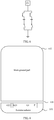
FIG. 8 is a schematic diagram of a first ground point of a terminal antenna according to an embodiment of the present invention; -
FIG. 9 is a schematic diagram of a terminal according to Embodiment 1 of the present invention; and -
FIG. 10 is a schematic diagram of a terminal according to Embodiment 2 of the present invention. - To provide an implementation solution for extending bandwidth of a terminal antenna, embodiments of the present invention provide a terminal. The following describes the embodiments of the present invention with reference to the accompanying drawings in the specification. It should be understood that the preferred embodiments described herein are merely for describing and explaining the present invention, but are not intended to limit the present invention. Moreover, the embodiments in this application and the features in the embodiments can be mutually combined when no conflict is caused.
- An embodiment of the present invention provides a terminal. As shown in
FIG. 1 , a metal back cover of the terminal has aslot 100. Theslot 100 divides the metal back cover into two parts. One of the two parts is used as anantenna radiator 101 of the terminal, and the other one is used as amain ground part 102. Theantenna radiator 101 has a signal feed point F, a first ground point G1, and at least one second ground point G2, so that an antenna of the terminal has four resonance points. - The signal feed point F is connected to a matching network, the first ground point G1 is grounded by using a switch device, and the second ground point G2 is grounded. A distance between the signal feed point F and the first ground point G1 is less than a distance between the signal feed point F and the second ground point G2, and none of the signal feed point F, the first ground point G1, and the second ground point G2 is located in a position, corresponding to an end of the
slot 100, on theantenna radiator 101. The end of theslot 100 is a position in which theslot 100 and a side frame of the terminal are connected. - In a specific embodiment of the present invention, the second ground point G2 of the
antenna radiator 101 may be directly grounded. During actual implementation, the second ground point G2 of theantenna radiator 101 may be directly grounded by being directly connected to a printed circuit board of the terminal, or the second ground point G2 of the antenna radiator may be directly grounded by being directly connected to themain ground part 102. That is, as shown inFIG. 2 , there may be no connection point between the two parts of the metal back cover of the terminal; or as shown inFIG. 3 , there may be a connection point in theslot 100 and in a position, corresponding to the second ground point G2, of theantenna radiator 101. - In another specific embodiment of the present invention, the second ground point G2 of the
antenna radiator 101 may also be grounded by using a fixed capacitor and/or a fixed inductor. For example, as shown inFIG. 4 , the second ground point G2 is grounded by using an LC filter formed by a fixed capacitor and a fixed inductor. In another specific embodiment of the present invention, the second ground point G2 of theantenna radiator 101 may also be grounded by using an adjustable device. For example, as shown inFIG. 5 , the second ground point G2 is grounded by using a variable capacitor or a switch device, so that a resonance coverage area can be enlarged. - Further, as shown in
FIG. 6 , theantenna radiator 101 may have a third ground point G3 in addition to the signal feed point F, the first ground point G1, and the second ground point G2, and the third ground point G3 is grounded. Moreover, the third ground point G3 is located in the position, corresponding to the end of theslot 100, on theantenna radiator 101. - In a specific embodiment of the present invention, the third ground point G3 of the
antenna radiator 101 may be directly grounded. During actual implementation, the third ground point G3 of theantenna radiator 101 may be directly grounded by being directly connected to the printed circuit board of the terminal, or the third ground point G3 of the antenna radiator may be directly grounded by being directly connected to themain ground part 102. That is, as shown inFIG. 7 , there may be a connection point between the two parts of the metal back cover of the terminal at the end of theslot 100 and in a position, corresponding to the third ground point G3, of theantenna radiator 101. - In another specific embodiment of the present invention, the third ground point G3 of the
antenna radiator 101 may also be grounded by using a fixed capacitor and/or a fixed inductor, for example, grounded by using an LC filter formed by a fixed capacitor and a fixed inductor. In another specific embodiment of the present invention, the third ground point G3 of theantenna radiator 101 may also be grounded by using an adjustable device, for example, grounded by using a variable capacitor or a switch device. This is not illustrated or described in detail herein. - Further, according to a requirement of an actual application scenario, in addition to the switch device, an inductor and a capacitor may be connected into a ground branch of the first ground point G1 of the
antenna radiator 101, that is, the first ground point G1 may be specifically grounded by using the inductor and/or the capacitor, and the switch device. For example, as shown inFIG. 8 , the switch device may be specifically a double-pole double-throw DPDT switch. It should be noted that the switch device in the ground branch of the first ground point G1 may be specifically the double-pole double-throw DPDT switch shown inFIG. 8 , or may be a single-pole single-throw SPST switch, a single-pole double-throw SPDT switch, a single-pole four-throw SP4T switch, or the like. This is not specifically limited by the present invention. - When the switch device in the ground branch of the first ground point G1 of the
antenna radiator 101 is off and the first ground point G1 is in an open circuit, the terminal antenna is in a low-frequency operating state. When the switch device in the ground branch of the first ground point G1 of theantenna radiator 101 is on and the first ground point G1 is short-circuited to ground, the terminal antenna is in a high-frequency operating state. That is, an operating status of the terminal antenna can be controlled by controlling a status of the switch device in the ground branch of the first ground point G1 of theantenna radiator 101. - The matching network connected to the signal feed point F of the
antenna radiator 101 includes a capacitor, and may further include an inductor. During specific implementation, the matching network may be a variable capacitor, so as to facilitate impedance matching. - The terminal provided by the present invention is described in the following with reference to the accompanying drawings by using specific embodiments as examples.
- A terminal provided by Embodiment 1 of the present invention is shown in
FIG. 9 . There is no connection point between two parts of a metal back cover of the terminal. Anantenna radiator 101 has a signal feed point F, a first ground point G1, and two second ground points G21 and G22. The signal feed point F is connected to a variable capacitor, the first ground point G1 is grounded by using a double-pole double-throw DPDT switch, and the two second ground points G21 and G22 are both directly grounded. During specific implementation, the first ground point G1 may be grounded by being connected to a printed circuit board of the terminal by using the double-pole double-throw DPDT switch. The second ground point G21 may be grounded by being connected to the printed circuit board of the terminal. The second ground point G22 of a terminal antenna may be grounded by being connected to amain ground part 102 of the metal back cover of the terminal by using a mechanical part. - When the double-pole double-throw DPDT switch in a ground branch of the first ground point G1 of the
antenna radiator 101 is off and the first ground point G1 is in an open circuit, the terminal antenna is in a low-frequency operating state. In this case, the signal feed point F and the two second ground points G21 and G22 are short-circuit points, two ends of theslot 100 are open-circuit points, and the following resonances may be formed in the terminal antenna: - 1. A resonance in a left-handed mode is formed between a distributed inductor between the signal feed point F and a closest short-circuit point, that is, the second ground point G21, and a variable capacitor connected to the signal feed point F, and a resonance frequency is f l1.
A value of the resonance frequency f l1 may be adjusted by adjusting a distance between the signal feed point F and the second ground point G21. A larger distance between the signal feed point F and the second ground point G21 leads to a smaller resonance frequency f l1, and a smaller distance between the signal feed point F and the second ground point G21 leads to a larger resonance frequency f l1. - 2. A resonance in a slot mode is formed between a left end of the
slot 100 and a closest short-circuit point, that is, the second ground point G22, and a resonance frequency is f l2 and corresponds to 1/4 of a guided-wave wavelength. The guided-wave wavelength is a signal wavelength of a central frequency of expected bandwidth of the terminal antenna.
A value of the resonance frequency f l2 may be adjusted by adjusting a distance between the left end of theslot 100 and the second ground point G22. A larger distance between the left end of theslot 100 and the second ground point G22 leads to a smaller resonance frequency f l2, and a smaller distance between the left end of theslot 100 and the second ground point G22 leads to a larger resonance frequency ji2. - 3. A resonance in the slot mode is formed between the signal feed point F and the second ground point G22, and a resonance frequency is f l3 and corresponds to 1/2 of the guided-wave wavelength.
A value of the resonance frequency f l3 may be adjusted by adjusting a distance between the signal feed point F and the second ground point G22. A larger distance between the signal feed point F and the second ground point G22 leads to a smaller resonance frequency f l3, and a smaller distance between the signal feed point F and the second ground point G22 leads to a larger resonance frequency f l3. - 4. A resonance in the slot mode is formed between a right end of the
slot 100 and a closest short-circuit point, that is, the signal feed point F, and a resonance frequency is f l4 and corresponds to 1/4 of the guided-wave wavelength.
A value of the resonance frequency f l4 may be adjusted by adjusting a distance between the right end of theslot 100 and the signal feed point F. A larger distance between the right end of theslot 100 and the signal feed point F leads to a smaller resonance frequency f l4, and a smaller distance between the left end of theslot 100 and the signal feed point F leads to a larger resonance frequency f l4. - That is, in the low-frequency operating state, the terminal antenna has one resonance point in the left-handed mode and three resonance points in the slot mode.
- When the double-pole double-throw DPDT switch in the ground branch of the first ground point G1 of the
antenna radiator 101 is on and the first ground point G1 is short-circuited to ground, the terminal antenna is in a high-frequency operating state. In this case, the signal feed point F, the first ground point G1, and the two second ground points G21 and G22 are all short-circuit points, the two ends of theslot 100 are open-circuit points, and the following resonances may be formed in the terminal antenna: - 1. A resonance in the left-handed mode is formed between a distributed inductor between the signal feed point F and a closest short-circuit point, that is, the first ground point G1, and the variable capacitor connected to the signal feed point F, and a resonance frequency is f h1.
A value of the resonance frequency f h1 may be adjusted by adjusting a distance between the signal feed point F and the first ground point G1. A larger distance between the signal feed point F and the first ground point G1 leads to a smaller resonance frequency f h1, and a smaller distance between the signal feed point F and the first ground point G1 leads to a larger resonance frequency f h1. - 2. A resonance in the slot mode is formed between the signal feed point F and the second ground point G22, and a resonance frequency is f h2 and corresponds to 1/2 of the guided-wave wavelength.
A value of the resonance frequency f h2 may be adjusted by adjusting a distance between the signal feed point F and the second ground point G22. A larger distance between the signal feed point F and the second ground point G22 leads to a smaller resonance frequency f h2, and a smaller distance between the signal feed point F and the second ground point G22 leads to a larger resonance frequency f h2. - 3. A resonance in the slot mode is formed between the left end of the
slot 100 and a closest short-circuit point, that is, the second ground point G22, and a resonance frequency is f h3 and corresponds to 1/4 of the guided-wave wavelength.
A value of the resonance frequency f h3 may be adjusted by adjusting a distance between the left end of theslot 100 and the second ground point G22. A larger distance between the left end of theslot 100 and the second ground point G22 leads to a smaller resonance frequency f h3, and a smaller distance between the left end of theslot 100 and the second ground point G22 leads to a larger resonance frequency f h3. - 4. A resonance in the slot mode is formed between the right end of the
slot 100 and a closest short-circuit point, that is, the signal feed point F, and a resonance frequency is f h4 and corresponds to 1/4 of the guided-wave wavelength.
A value of the resonance frequency f h4 may be adjusted by adjusting a distance between the right end of theslot 100 and the signal feed point F. A larger distance between the right end of theslot 100 and the signal feed point F leads to a smaller resonance frequency f h4, and a smaller distance between the right end of theslot 100 and the signal feed point F leads to a larger resonance frequency f h4. - That is, in the high-frequency operating state, the terminal antenna can also have one resonance point in the left-handed mode and three resonance points in the slot mode.
- During actual implementation, specific positions of the signal feed point F, the first ground point G1, and the two second ground points G21 and G22 of the
antenna radiator 101 may be set according to a requirement of an actual application scenario. - For example, when the signal feed point F is 8.3 mm distant from the right end of the
slot 100, the second ground point G21 is 30 mm distant from the left end of theslot 100, the second ground point G22 is 20.8 mm distant from the left end of theslot 100, and a change range of the variable capacitor connected to the signal feed point F is 0.7 pF - 2.7 pF, the terminal antenna can achieve 1710 MHz - 2700 MHz full-band coverage. - A terminal provided by Embodiment 2 of the present invention is shown in
FIG. 10 . Compared with the terminal inFIG. 9 of Embodiment 1, a difference lies in that there is a connection point that is between the two parts of the metal back cover of the terminal and that is at the left end of theslot 100. Due to existence of the connection point, this is equivalent to that theantenna radiator 101 has an additional third ground point G3 that is directly grounded. In this case, a resonance in a slot mode that is formed between the left end of theslot 100 and the second ground point G22 corresponds to 1/2 of a guided-wave wavelength. - Further, a ground point that is grounded by using an adjustable device may be further added between the left end of the
slot 100 and the second ground point G22, and an electrical length between the left end of theslot 100 and the second ground point G22 can be changed, so as to adjust the resonance in the slot mode and change a resonance frequency. - In summary, with use of the terminal provided by the embodiments of the present invention, no matter whether a terminal antenna is in a low-frequency or high-frequency operating state, the terminal antenna can have four resonance points: one resonance point in a left-handed mode and three resonance points in a slot mode. Compared with the prior art, bandwidth of the terminal antenna can be extended, and performance of the terminal antenna can be improved.
- Persons skilled in the art should understand that although preferred embodiments of the present invention have been described, persons skilled in the art can make changes and modifications to these embodiments once they learn the basic inventive concept. Therefore, the following claims are intended to be construed as to cover the preferred embodiments and all changes and modifications falling within the scope of the present invention.
- Obviously, persons skilled in the art can make various modifications and variations to the embodiments of the present invention without departing from the spirit and scope of the embodiments of the present invention. The present invention is intended to cover these modifications and variations provided that they fall within the scope of protection defined by the following claims and their equivalent technologies.
Claims (8)
- A terminal, wherein a metal back cover of the terminal has a slot, the slot divides the metal back cover into two parts, and one of the two parts is used as an antenna radiator of the terminal; and the antenna radiator has a signal feed point, a first ground point, and at least one second ground point, so that an antenna of the terminal has four resonance points, wherein
the signal feed point is connected to a matching network, the first ground point is grounded by using a switch device, and the second ground point is grounded; and a distance between the signal feed point and the first ground point is less than a distance between the signal feed point and the second ground point, and none of the signal feed point, the first ground point, and the second ground point is located in a position, corresponding to an end of the slot, on the antenna radiator. - The terminal according to claim 1, wherein the second ground point of the antenna radiator is specifically grounded by using an adjustable device.
- The terminal according to claim 1, wherein the second ground point of the antenna radiator is specifically grounded by using a fixed capacitor and/or a fixed inductor.
- The terminal according to any one of claims 1 to 3, wherein the antenna radiator further has a third ground point, the third ground point is grounded, and the third ground point is located in the position, corresponding to the end of the slot, on the antenna radiator.
- The terminal according to claim 4, wherein the third ground point of the antenna radiator is specifically grounded by using an adjustable device.
- The terminal according to claim 4, wherein the third ground point of the antenna radiator is specifically grounded by using a fixed capacitor and/or a fixed inductor.
- The terminal according to any one of claims 1 to 6, wherein the first ground point of the antenna radiator is specifically grounded by using an inductor and/or a capacitor, and the switch device.
- The terminal according to any one of claims 1 to 7, wherein the matching network connected to the signal feed point of the antenna radiator is specifically a variable capacitor.
Applications Claiming Priority (1)
| Application Number | Priority Date | Filing Date | Title |
|---|---|---|---|
| PCT/CN2015/075390 WO2016154851A1 (en) | 2015-03-30 | 2015-03-30 | Terminal |
Publications (3)
| Publication Number | Publication Date |
|---|---|
| EP3252867A1 true EP3252867A1 (en) | 2017-12-06 |
| EP3252867A4 EP3252867A4 (en) | 2018-02-21 |
| EP3252867B1 EP3252867B1 (en) | 2019-10-02 |
Family
ID=57003886
Family Applications (1)
| Application Number | Title | Priority Date | Filing Date |
|---|---|---|---|
| EP15886838.0A Active EP3252867B1 (en) | 2015-03-30 | 2015-03-30 | Terminal |
Country Status (5)
| Country | Link |
|---|---|
| US (1) | US10256534B2 (en) |
| EP (1) | EP3252867B1 (en) |
| CN (1) | CN106575821B (en) |
| BR (1) | BR112017019826B1 (en) |
| WO (1) | WO2016154851A1 (en) |
Families Citing this family (17)
| Publication number | Priority date | Publication date | Assignee | Title |
|---|---|---|---|---|
| WO2018090669A1 (en) | 2016-11-18 | 2018-05-24 | Guangdong Oppo Mobile Telecommunications Corp., Ltd. | Antenna device for mobile terminal and mobile terminal |
| WO2018120774A1 (en) * | 2016-12-28 | 2018-07-05 | Guangdong Oppo Mobile Telecommunications Corp., Ltd. | Antenna device for mobile terminal and mobile terminal |
| CN106953179B (en) * | 2017-03-03 | 2021-06-08 | 深圳天珑无线科技有限公司 | Single-port antenna switching system and method |
| KR102364559B1 (en) * | 2017-03-24 | 2022-02-21 | 삼성전자주식회사 | Electronic device comprising antenna |
| KR102307730B1 (en) * | 2017-04-10 | 2021-10-05 | 삼성전자주식회사 | An electronic device comprising antenna which is using an electrically conductive material included in a housing of the electronic device |
| CN110998973B (en) * | 2017-10-09 | 2022-03-08 | 华为技术有限公司 | Antenna device and mobile terminal |
| SE1751340A1 (en) * | 2017-10-30 | 2019-03-26 | Smarteq Wireless Ab | Ground plane independent antenna |
| CN108376830A (en) * | 2018-02-08 | 2018-08-07 | 广东欧珀移动通信有限公司 | Antenna device for electronic equipment and electronic equipment |
| CN108376834A (en) * | 2018-02-08 | 2018-08-07 | 广东欧珀移动通信有限公司 | Antenna device of electronic equipment and electronic equipment |
| CN108493617A (en) * | 2018-05-24 | 2018-09-04 | 努比亚技术有限公司 | A kind of antenna system and communication terminal |
| CN110718761B (en) | 2018-07-11 | 2021-11-09 | 华为技术有限公司 | Antenna device and mobile terminal |
| CN110767980B (en) * | 2018-07-27 | 2021-11-02 | 深圳富泰宏精密工业有限公司 | Antenna structure and wireless communication device with same |
| CN113745809B (en) * | 2020-05-27 | 2023-08-22 | 华为技术有限公司 | Electronic equipment |
| CN112290200B (en) * | 2020-10-14 | 2022-03-18 | 珠海格力电器股份有限公司 | Antenna structure and electronic equipment |
| CN115249879A (en) * | 2021-04-28 | 2022-10-28 | Oppo广东移动通信有限公司 | Antenna assembly and electronic equipment |
| CN116799484A (en) * | 2022-03-16 | 2023-09-22 | 中兴通讯股份有限公司 | A multi-frequency multiplexing antenna and mobile terminal |
| TWI860527B (en) * | 2022-06-09 | 2024-11-01 | 啓碁科技股份有限公司 | Antenna structure |
Family Cites Families (16)
| Publication number | Priority date | Publication date | Assignee | Title |
|---|---|---|---|---|
| US6961022B1 (en) * | 2005-03-23 | 2005-11-01 | Motorola, Inc. | Antenna radiator assembly and radio communications device |
| KR101119267B1 (en) * | 2010-04-13 | 2012-03-16 | 고려대학교 산학협력단 | Dielectric resonant antenna using matching substrate |
| US8489162B1 (en) | 2010-08-17 | 2013-07-16 | Amazon Technologies, Inc. | Slot antenna within existing device component |
| KR101606145B1 (en) * | 2010-10-20 | 2016-03-24 | 삼성전자주식회사 | Antenna device for portable terminal |
| TWI448008B (en) | 2010-12-17 | 2014-08-01 | Htc Corp | Handheld device and planar antenna thereof |
| EP3525285B1 (en) * | 2012-06-21 | 2021-05-12 | LG Electronics Inc. | Antenna device and mobile terminal having the same |
| US9413066B2 (en) * | 2012-07-19 | 2016-08-09 | Blackberry Limited | Method and apparatus for beam forming and antenna tuning in a communication device |
| US9716307B2 (en) | 2012-11-08 | 2017-07-25 | Htc Corporation | Mobile device and antenna structure |
| CN103178344A (en) * | 2013-04-01 | 2013-06-26 | 昆山睿翔讯通通信技术有限公司 | Multi-frequency-band rear metal cover mobile phone antenna |
| CN103401059B (en) | 2013-07-29 | 2015-08-26 | 广东欧珀移动通信有限公司 | Antenna device for full metal shell |
| CN203466294U (en) * | 2013-08-22 | 2014-03-05 | 深圳富泰宏精密工业有限公司 | Adjustable antenna and wireless communication device therewith |
| CN104659483A (en) | 2013-11-22 | 2015-05-27 | 英业达科技有限公司 | Electronic device |
| CN203747027U (en) | 2013-12-24 | 2014-07-30 | 上海安费诺永亿通讯电子有限公司 | All-metal mobile terminal double-slit antenna |
| CN103700925B (en) | 2013-12-24 | 2016-06-22 | 上海安费诺永亿通讯电子有限公司 | A kind of all-metal mobile terminal double-slit antenna |
| US10347969B2 (en) * | 2014-07-31 | 2019-07-09 | Huawei Technologies Co., Ltd. | Mobile terminal with an antenna having multiple radiators |
| CN204216212U (en) | 2014-11-12 | 2015-03-18 | 瑞声声学科技(苏州)有限公司 | Communication terminal |
-
2015
- 2015-03-30 WO PCT/CN2015/075390 patent/WO2016154851A1/en not_active Ceased
- 2015-03-30 CN CN201580036292.7A patent/CN106575821B/en active Active
- 2015-03-30 BR BR112017019826-6A patent/BR112017019826B1/en not_active IP Right Cessation
- 2015-03-30 US US15/560,405 patent/US10256534B2/en active Active
- 2015-03-30 EP EP15886838.0A patent/EP3252867B1/en active Active
Also Published As
| Publication number | Publication date |
|---|---|
| EP3252867A4 (en) | 2018-02-21 |
| US10256534B2 (en) | 2019-04-09 |
| US20180069306A1 (en) | 2018-03-08 |
| CN106575821A (en) | 2017-04-19 |
| CN106575821B (en) | 2019-11-05 |
| BR112017019826B1 (en) | 2022-11-16 |
| BR112017019826A2 (en) | 2018-07-17 |
| EP3252867B1 (en) | 2019-10-02 |
| WO2016154851A1 (en) | 2016-10-06 |
Similar Documents
| Publication | Publication Date | Title |
|---|---|---|
| EP3252867A1 (en) | Terminal | |
| EP3107150B1 (en) | Electronic device | |
| AU2017405558B2 (en) | Antenna of mobile terminal and mobile terminal | |
| US9680222B2 (en) | Antenna structure and wireless communication device using the same | |
| US10381701B2 (en) | Filter circuit and frequency switching method | |
| US9673512B2 (en) | Antenna assembly and wireless communication device employing same | |
| CN105789831A (en) | Mobile terminal and antenna structure thereof | |
| WO2021082560A1 (en) | Foldable electronic device | |
| US20140184449A1 (en) | Antenna structure for using with a metal frame of a mobile phone | |
| EP3767742A1 (en) | Antenna device and mobile terminal | |
| EP3709441B1 (en) | Multi-frequency antenna and mobile terminal | |
| CN110299618B (en) | Antenna system and terminal | |
| EP3333976B1 (en) | Metal housing, housing antenna, and electronic device | |
| WO2012169186A1 (en) | Antenna device | |
| EP3220478B1 (en) | Diversity antenna | |
| US20170264975A1 (en) | Communication device with narrow-ground-clearance antenna element | |
| EP3188313A1 (en) | Multi-band antenna and communication terminal | |
| US9780862B2 (en) | Antenna structure and wireless communication device using the same | |
| CN104466361B (en) | A kind of mobile phone and its antenna | |
| JP2017505034A (en) | Antenna and terminal device | |
| EP3828996A1 (en) | Antenna apparatus and terminal | |
| KR20110068246A (en) | Broadband antenna | |
| CN109075425B (en) | An antenna for a mobile terminal and a method for using the same, and a mobile terminal | |
| CN205811060U (en) | A kind of directional antenna assembly | |
| CN104577340B (en) | Multiband tunable antenna and wireless communication device |
Legal Events
| Date | Code | Title | Description |
|---|---|---|---|
| STAA | Information on the status of an ep patent application or granted ep patent |
Free format text: STATUS: THE INTERNATIONAL PUBLICATION HAS BEEN MADE |
|
| PUAI | Public reference made under article 153(3) epc to a published international application that has entered the european phase |
Free format text: ORIGINAL CODE: 0009012 |
|
| STAA | Information on the status of an ep patent application or granted ep patent |
Free format text: STATUS: REQUEST FOR EXAMINATION WAS MADE |
|
| 17P | Request for examination filed |
Effective date: 20170830 |
|
| AK | Designated contracting states |
Kind code of ref document: A1 Designated state(s): AL AT BE BG CH CY CZ DE DK EE ES FI FR GB GR HR HU IE IS IT LI LT LU LV MC MK MT NL NO PL PT RO RS SE SI SK SM TR |
|
| AX | Request for extension of the european patent |
Extension state: BA ME |
|
| RIC1 | Information provided on ipc code assigned before grant |
Ipc: H01Q 1/44 20060101AFI20180110BHEP |
|
| A4 | Supplementary search report drawn up and despatched |
Effective date: 20180118 |
|
| DAV | Request for validation of the european patent (deleted) | ||
| DAX | Request for extension of the european patent (deleted) | ||
| GRAP | Despatch of communication of intention to grant a patent |
Free format text: ORIGINAL CODE: EPIDOSNIGR1 |
|
| STAA | Information on the status of an ep patent application or granted ep patent |
Free format text: STATUS: GRANT OF PATENT IS INTENDED |
|
| INTG | Intention to grant announced |
Effective date: 20190426 |
|
| GRAS | Grant fee paid |
Free format text: ORIGINAL CODE: EPIDOSNIGR3 |
|
| GRAA | (expected) grant |
Free format text: ORIGINAL CODE: 0009210 |
|
| STAA | Information on the status of an ep patent application or granted ep patent |
Free format text: STATUS: THE PATENT HAS BEEN GRANTED |
|
| AK | Designated contracting states |
Kind code of ref document: B1 Designated state(s): AL AT BE BG CH CY CZ DE DK EE ES FI FR GB GR HR HU IE IS IT LI LT LU LV MC MK MT NL NO PL PT RO RS SE SI SK SM TR |
|
| REG | Reference to a national code |
Ref country code: GB Ref legal event code: FG4D |
|
| REG | Reference to a national code |
Ref country code: CH Ref legal event code: EP Ref country code: AT Ref legal event code: REF Ref document number: 1187229 Country of ref document: AT Kind code of ref document: T Effective date: 20191015 |
|
| REG | Reference to a national code |
Ref country code: DE Ref legal event code: R096 Ref document number: 602015039305 Country of ref document: DE |
|
| REG | Reference to a national code |
Ref country code: IE Ref legal event code: FG4D |
|
| REG | Reference to a national code |
Ref country code: NL Ref legal event code: FP |
|
| REG | Reference to a national code |
Ref country code: LT Ref legal event code: MG4D |
|
| REG | Reference to a national code |
Ref country code: AT Ref legal event code: MK05 Ref document number: 1187229 Country of ref document: AT Kind code of ref document: T Effective date: 20191002 |
|
| PG25 | Lapsed in a contracting state [announced via postgrant information from national office to epo] |
Ref country code: GR Free format text: LAPSE BECAUSE OF FAILURE TO SUBMIT A TRANSLATION OF THE DESCRIPTION OR TO PAY THE FEE WITHIN THE PRESCRIBED TIME-LIMIT Effective date: 20200103 Ref country code: ES Free format text: LAPSE BECAUSE OF FAILURE TO SUBMIT A TRANSLATION OF THE DESCRIPTION OR TO PAY THE FEE WITHIN THE PRESCRIBED TIME-LIMIT Effective date: 20191002 Ref country code: PL Free format text: LAPSE BECAUSE OF FAILURE TO SUBMIT A TRANSLATION OF THE DESCRIPTION OR TO PAY THE FEE WITHIN THE PRESCRIBED TIME-LIMIT Effective date: 20191002 Ref country code: LT Free format text: LAPSE BECAUSE OF FAILURE TO SUBMIT A TRANSLATION OF THE DESCRIPTION OR TO PAY THE FEE WITHIN THE PRESCRIBED TIME-LIMIT Effective date: 20191002 Ref country code: NO Free format text: LAPSE BECAUSE OF FAILURE TO SUBMIT A TRANSLATION OF THE DESCRIPTION OR TO PAY THE FEE WITHIN THE PRESCRIBED TIME-LIMIT Effective date: 20200102 Ref country code: LV Free format text: LAPSE BECAUSE OF FAILURE TO SUBMIT A TRANSLATION OF THE DESCRIPTION OR TO PAY THE FEE WITHIN THE PRESCRIBED TIME-LIMIT Effective date: 20191002 Ref country code: SE Free format text: LAPSE BECAUSE OF FAILURE TO SUBMIT A TRANSLATION OF THE DESCRIPTION OR TO PAY THE FEE WITHIN THE PRESCRIBED TIME-LIMIT Effective date: 20191002 Ref country code: PT Free format text: LAPSE BECAUSE OF FAILURE TO SUBMIT A TRANSLATION OF THE DESCRIPTION OR TO PAY THE FEE WITHIN THE PRESCRIBED TIME-LIMIT Effective date: 20200203 Ref country code: FI Free format text: LAPSE BECAUSE OF FAILURE TO SUBMIT A TRANSLATION OF THE DESCRIPTION OR TO PAY THE FEE WITHIN THE PRESCRIBED TIME-LIMIT Effective date: 20191002 Ref country code: AT Free format text: LAPSE BECAUSE OF FAILURE TO SUBMIT A TRANSLATION OF THE DESCRIPTION OR TO PAY THE FEE WITHIN THE PRESCRIBED TIME-LIMIT Effective date: 20191002 Ref country code: BG Free format text: LAPSE BECAUSE OF FAILURE TO SUBMIT A TRANSLATION OF THE DESCRIPTION OR TO PAY THE FEE WITHIN THE PRESCRIBED TIME-LIMIT Effective date: 20200102 |
|
| PG25 | Lapsed in a contracting state [announced via postgrant information from national office to epo] |
Ref country code: CZ Free format text: LAPSE BECAUSE OF FAILURE TO SUBMIT A TRANSLATION OF THE DESCRIPTION OR TO PAY THE FEE WITHIN THE PRESCRIBED TIME-LIMIT Effective date: 20191002 Ref country code: RS Free format text: LAPSE BECAUSE OF FAILURE TO SUBMIT A TRANSLATION OF THE DESCRIPTION OR TO PAY THE FEE WITHIN THE PRESCRIBED TIME-LIMIT Effective date: 20191002 Ref country code: IS Free format text: LAPSE BECAUSE OF FAILURE TO SUBMIT A TRANSLATION OF THE DESCRIPTION OR TO PAY THE FEE WITHIN THE PRESCRIBED TIME-LIMIT Effective date: 20200224 Ref country code: HR Free format text: LAPSE BECAUSE OF FAILURE TO SUBMIT A TRANSLATION OF THE DESCRIPTION OR TO PAY THE FEE WITHIN THE PRESCRIBED TIME-LIMIT Effective date: 20191002 |
|
| PG25 | Lapsed in a contracting state [announced via postgrant information from national office to epo] |
Ref country code: AL Free format text: LAPSE BECAUSE OF FAILURE TO SUBMIT A TRANSLATION OF THE DESCRIPTION OR TO PAY THE FEE WITHIN THE PRESCRIBED TIME-LIMIT Effective date: 20191002 |
|
| REG | Reference to a national code |
Ref country code: DE Ref legal event code: R097 Ref document number: 602015039305 Country of ref document: DE |
|
| PG2D | Information on lapse in contracting state deleted |
Ref country code: IS |
|
| PG25 | Lapsed in a contracting state [announced via postgrant information from national office to epo] |
Ref country code: EE Free format text: LAPSE BECAUSE OF FAILURE TO SUBMIT A TRANSLATION OF THE DESCRIPTION OR TO PAY THE FEE WITHIN THE PRESCRIBED TIME-LIMIT Effective date: 20191002 Ref country code: DK Free format text: LAPSE BECAUSE OF FAILURE TO SUBMIT A TRANSLATION OF THE DESCRIPTION OR TO PAY THE FEE WITHIN THE PRESCRIBED TIME-LIMIT Effective date: 20191002 Ref country code: RO Free format text: LAPSE BECAUSE OF FAILURE TO SUBMIT A TRANSLATION OF THE DESCRIPTION OR TO PAY THE FEE WITHIN THE PRESCRIBED TIME-LIMIT Effective date: 20191002 Ref country code: IS Free format text: LAPSE BECAUSE OF FAILURE TO SUBMIT A TRANSLATION OF THE DESCRIPTION OR TO PAY THE FEE WITHIN THE PRESCRIBED TIME-LIMIT Effective date: 20200202 |
|
| PLBE | No opposition filed within time limit |
Free format text: ORIGINAL CODE: 0009261 |
|
| STAA | Information on the status of an ep patent application or granted ep patent |
Free format text: STATUS: NO OPPOSITION FILED WITHIN TIME LIMIT |
|
| PG25 | Lapsed in a contracting state [announced via postgrant information from national office to epo] |
Ref country code: SM Free format text: LAPSE BECAUSE OF FAILURE TO SUBMIT A TRANSLATION OF THE DESCRIPTION OR TO PAY THE FEE WITHIN THE PRESCRIBED TIME-LIMIT Effective date: 20191002 Ref country code: SK Free format text: LAPSE BECAUSE OF FAILURE TO SUBMIT A TRANSLATION OF THE DESCRIPTION OR TO PAY THE FEE WITHIN THE PRESCRIBED TIME-LIMIT Effective date: 20191002 Ref country code: IT Free format text: LAPSE BECAUSE OF FAILURE TO SUBMIT A TRANSLATION OF THE DESCRIPTION OR TO PAY THE FEE WITHIN THE PRESCRIBED TIME-LIMIT Effective date: 20191002 |
|
| 26N | No opposition filed |
Effective date: 20200703 |
|
| PG25 | Lapsed in a contracting state [announced via postgrant information from national office to epo] |
Ref country code: MC Free format text: LAPSE BECAUSE OF FAILURE TO SUBMIT A TRANSLATION OF THE DESCRIPTION OR TO PAY THE FEE WITHIN THE PRESCRIBED TIME-LIMIT Effective date: 20191002 |
|
| REG | Reference to a national code |
Ref country code: CH Ref legal event code: PL |
|
| PG25 | Lapsed in a contracting state [announced via postgrant information from national office to epo] |
Ref country code: SI Free format text: LAPSE BECAUSE OF FAILURE TO SUBMIT A TRANSLATION OF THE DESCRIPTION OR TO PAY THE FEE WITHIN THE PRESCRIBED TIME-LIMIT Effective date: 20191002 |
|
| REG | Reference to a national code |
Ref country code: BE Ref legal event code: MM Effective date: 20200331 |
|
| PG25 | Lapsed in a contracting state [announced via postgrant information from national office to epo] |
Ref country code: LU Free format text: LAPSE BECAUSE OF NON-PAYMENT OF DUE FEES Effective date: 20200330 |
|
| PG25 | Lapsed in a contracting state [announced via postgrant information from national office to epo] |
Ref country code: IE Free format text: LAPSE BECAUSE OF NON-PAYMENT OF DUE FEES Effective date: 20200330 Ref country code: LI Free format text: LAPSE BECAUSE OF NON-PAYMENT OF DUE FEES Effective date: 20200331 Ref country code: CH Free format text: LAPSE BECAUSE OF NON-PAYMENT OF DUE FEES Effective date: 20200331 |
|
| PG25 | Lapsed in a contracting state [announced via postgrant information from national office to epo] |
Ref country code: BE Free format text: LAPSE BECAUSE OF NON-PAYMENT OF DUE FEES Effective date: 20200331 |
|
| PG25 | Lapsed in a contracting state [announced via postgrant information from national office to epo] |
Ref country code: TR Free format text: LAPSE BECAUSE OF FAILURE TO SUBMIT A TRANSLATION OF THE DESCRIPTION OR TO PAY THE FEE WITHIN THE PRESCRIBED TIME-LIMIT Effective date: 20191002 Ref country code: MT Free format text: LAPSE BECAUSE OF FAILURE TO SUBMIT A TRANSLATION OF THE DESCRIPTION OR TO PAY THE FEE WITHIN THE PRESCRIBED TIME-LIMIT Effective date: 20191002 Ref country code: CY Free format text: LAPSE BECAUSE OF FAILURE TO SUBMIT A TRANSLATION OF THE DESCRIPTION OR TO PAY THE FEE WITHIN THE PRESCRIBED TIME-LIMIT Effective date: 20191002 |
|
| PG25 | Lapsed in a contracting state [announced via postgrant information from national office to epo] |
Ref country code: MK Free format text: LAPSE BECAUSE OF FAILURE TO SUBMIT A TRANSLATION OF THE DESCRIPTION OR TO PAY THE FEE WITHIN THE PRESCRIBED TIME-LIMIT Effective date: 20191002 |
|
| PGFP | Annual fee paid to national office [announced via postgrant information from national office to epo] |
Ref country code: NL Payment date: 20240214 Year of fee payment: 10 |
|
| PGFP | Annual fee paid to national office [announced via postgrant information from national office to epo] |
Ref country code: DE Payment date: 20240206 Year of fee payment: 10 |
|
| PGFP | Annual fee paid to national office [announced via postgrant information from national office to epo] |
Ref country code: FR Payment date: 20240213 Year of fee payment: 10 |
|
| REG | Reference to a national code |
Ref country code: DE Ref legal event code: R119 Ref document number: 602015039305 Country of ref document: DE |
|
| REG | Reference to a national code |
Ref country code: NL Ref legal event code: MM Effective date: 20250401 |
|
| PG25 | Lapsed in a contracting state [announced via postgrant information from national office to epo] |
Ref country code: NL Free format text: LAPSE BECAUSE OF NON-PAYMENT OF DUE FEES Effective date: 20250401 |
|
| PG25 | Lapsed in a contracting state [announced via postgrant information from national office to epo] |
Ref country code: DE Free format text: LAPSE BECAUSE OF NON-PAYMENT OF DUE FEES Effective date: 20251001 |
|
| PG25 | Lapsed in a contracting state [announced via postgrant information from national office to epo] |
Ref country code: FR Free format text: LAPSE BECAUSE OF NON-PAYMENT OF DUE FEES Effective date: 20250331 |
|
| PGFP | Annual fee paid to national office [announced via postgrant information from national office to epo] |
Ref country code: GB Payment date: 20260209 Year of fee payment: 12 |