EP3252776A1 - Memory device with progressive row reading and related reading method - Google Patents
Memory device with progressive row reading and related reading method Download PDFInfo
- Publication number
- EP3252776A1 EP3252776A1 EP16206895.1A EP16206895A EP3252776A1 EP 3252776 A1 EP3252776 A1 EP 3252776A1 EP 16206895 A EP16206895 A EP 16206895A EP 3252776 A1 EP3252776 A1 EP 3252776A1
- Authority
- EP
- European Patent Office
- Prior art keywords
- dummy
- row
- charging
- memory
- word line
- Prior art date
- Legal status (The legal status is an assumption and is not a legal conclusion. Google has not performed a legal analysis and makes no representation as to the accuracy of the status listed.)
- Granted
Links
Images

Classifications
-
- G—PHYSICS
- G11—INFORMATION STORAGE
- G11C—STATIC STORES
- G11C16/00—Erasable programmable read-only memories
- G11C16/02—Erasable programmable read-only memories electrically programmable
- G11C16/06—Auxiliary circuits, e.g. for writing into memory
- G11C16/26—Sensing or reading circuits; Data output circuits
- G11C16/28—Sensing or reading circuits; Data output circuits using differential sensing or reference cells, e.g. dummy cells
-
- G—PHYSICS
- G11—INFORMATION STORAGE
- G11C—STATIC STORES
- G11C11/00—Digital stores characterised by the use of particular electric or magnetic storage elements; Storage elements therefor
- G11C11/56—Digital stores characterised by the use of particular electric or magnetic storage elements; Storage elements therefor using storage elements with more than two stable states represented by steps, e.g. of voltage, current, phase, frequency
- G11C11/5621—Digital stores characterised by the use of particular electric or magnetic storage elements; Storage elements therefor using storage elements with more than two stable states represented by steps, e.g. of voltage, current, phase, frequency using charge storage in a floating gate
- G11C11/5642—Sensing or reading circuits; Data output circuits
-
- G—PHYSICS
- G11—INFORMATION STORAGE
- G11C—STATIC STORES
- G11C16/00—Erasable programmable read-only memories
- G11C16/02—Erasable programmable read-only memories electrically programmable
- G11C16/06—Auxiliary circuits, e.g. for writing into memory
- G11C16/08—Address circuits; Decoders; Word-line control circuits
-
- G—PHYSICS
- G11—INFORMATION STORAGE
- G11C—STATIC STORES
- G11C16/00—Erasable programmable read-only memories
- G11C16/02—Erasable programmable read-only memories electrically programmable
- G11C16/06—Auxiliary circuits, e.g. for writing into memory
- G11C16/26—Sensing or reading circuits; Data output circuits
-
- G—PHYSICS
- G11—INFORMATION STORAGE
- G11C—STATIC STORES
- G11C16/00—Erasable programmable read-only memories
- G11C16/02—Erasable programmable read-only memories electrically programmable
- G11C16/06—Auxiliary circuits, e.g. for writing into memory
- G11C16/32—Timing circuits
-
- G—PHYSICS
- G11—INFORMATION STORAGE
- G11C—STATIC STORES
- G11C7/00—Arrangements for writing information into, or reading information out from, a digital store
- G11C7/14—Dummy cell management; Sense reference voltage generators
-
- G—PHYSICS
- G11—INFORMATION STORAGE
- G11C—STATIC STORES
- G11C7/00—Arrangements for writing information into, or reading information out from, a digital store
- G11C7/22—Read-write [R-W] timing or clocking circuits; Read-write [R-W] control signal generators or management
- G11C7/227—Timing of memory operations based on dummy memory elements or replica circuits
-
- G—PHYSICS
- G11—INFORMATION STORAGE
- G11C—STATIC STORES
- G11C8/00—Arrangements for selecting an address in a digital store
- G11C8/08—Word line control circuits, e.g. drivers, boosters, pull-up circuits, pull-down circuits, precharging circuits, for word lines
-
- G—PHYSICS
- G11—INFORMATION STORAGE
- G11C—STATIC STORES
- G11C8/00—Arrangements for selecting an address in a digital store
- G11C8/14—Word line organisation; Word line lay-out
-
- G—PHYSICS
- G11—INFORMATION STORAGE
- G11C—STATIC STORES
- G11C16/00—Erasable programmable read-only memories
- G11C16/02—Erasable programmable read-only memories electrically programmable
- G11C16/06—Auxiliary circuits, e.g. for writing into memory
- G11C16/24—Bit-line control circuits
-
- G—PHYSICS
- G11—INFORMATION STORAGE
- G11C—STATIC STORES
- G11C7/00—Arrangements for writing information into, or reading information out from, a digital store
- G11C7/06—Sense amplifiers; Associated circuits, e.g. timing or triggering circuits
- G11C7/062—Differential amplifiers of non-latching type, e.g. comparators, long-tailed pairs
Definitions
- the present invention relates to a memory device in which a progressive row reading is implemented; moreover, the present invention regards a method for reading a memory device.
- a memory device 1 of a known type for example, of a non-volatile flash type, comprises a memory array 2 including a plurality of memory cells 3, which are arranged in rows and columns. Each row is coupled to a corresponding word line WL, whereas each column is coupled to a corresponding bit line BL.
- Each memory cell 3 is formed by a storage element, which is formed by a floating-gate transistor.
- the gate terminal of the floating-gate transistor is coupled to a respective word line WL, whereas a first conduction terminal is coupled to a respective bit line BL; in addition, a second conduction terminal of the floating-gate transistor is connected to a reference potential (for example, a ground).
- the gate terminals of the memory cells 3 of a same row are thus connected to a same word line WL; moreover, the first conduction terminals of the memory cells 3 of a same column are connected to a same bit line BL.
- a column-decoder circuit 4 and a row-decoder circuit 5 enable selection, on the basis of address signals received at input (designated as a whole by AS), of the memory cells 3, and in particular of the corresponding word lines WL and bit lines BL each time addressed, enabling biasing thereof at appropriate voltage and current values during the memory operations.
- both the column-decoder circuit 4 and the row-decoder circuit 5 are coupled to an address bus and are moreover provided with corresponding enable inputs, through which the circuits are notified of the fact that on the address bus a new address is present.
- the addresses and the signals for the enable inputs of the column-decoder circuit 4 and of the row-decoder circuit 5 are generated by a purposely provided circuitry (not shown).
- the column-decoder circuit 4 provides a read path, which forms conductive paths between the bit line BL of the memory array 2 each time selected and a read-amplifier circuit 10.
- the read-amplifier circuit 10 is designed to compare the current circulating in each memory cell 3 addressed with a reference current in order to determine the corresponding data item stored.
- the read-amplifier circuit 10 comprises a biasing stage 11, designed to bias the bit lines BL of the memory array 2, and a current-to-voltage (I/V) converter stage 12, which are now described limitedly to the functions that they perform in regard to a bit line BL of the memory array 2, and thus limitedly to the portions that co-operate with said bit line BL of the memory array 2, on the hypothesis of said bit line BL having been addressed, i.e., selected.
- I/V current-to-voltage
- the biasing stage 11 in turn comprises a biasing generator 13 and a pair of biasing transistors 14a, 14b, of an NMOS type in cascode configuration.
- the biasing generator 13 receives at input a voltage that may be boosted (in what follows referred to as "boosted voltage V boost "), for example by a charge-pump voltage-booster stage (not shown), and generates at output a biasing voltage V casc on a biasing node N p .
- the biasing generator 13 may receive directly a supply voltage V dd , of a value lower than that of the boosted voltage V boost .
- the control terminals of the biasing transistors 14a, 14b are both connected to the aforesaid biasing node N p so as to receive the biasing voltage V casc .
- a first biasing transistor 14a of the pair has a first conduction terminal coupled to the bit line BL, from which it receives a cell-reading current I cell , through the read path formed by the column-decoder circuit 4; moreover, the first biasing transistor 14a comprises a second conduction terminal, which is connected to a first comparison input IN a of the current-to-voltage converter stage 12.
- the second biasing transistor 14b of the pair has a respective first conduction terminal coupled to a current-reference generator 15 (or, alternatively, to a reference cell, here not illustrated), from which it receives a reference reading current I ref , and a second conduction terminal, which is connected to a second comparison input IN b of the current-to-voltage converter stage 12.
- the current-to-voltage converter stage 12 moreover has a supply input, on which it receives the supply voltage V dd , and is configured to make a comparison between the value of the cell-reading current I cell and the value of the reference reading current I ref , as well as for generating, on the basis of the result of this comparison, an output voltage V out .
- the cell-reading current I cell traverses the memory cell 3 actually addressed, but not the other memory cells 3 coupled to the bit line BL, and is a function of the data item stored therein.
- the read-amplifier circuit 10 further comprises a comparator stage 16, which receives at input the output voltage V out from the current-to-voltage converter stage 12 and generates, on the basis of the value (for example, positive or negative) of this output voltage V out , a digital reading signal S out representing the data item stored in the memory cell 3 addressed.
- a comparator stage 16 which receives at input the output voltage V out from the current-to-voltage converter stage 12 and generates, on the basis of the value (for example, positive or negative) of this output voltage V out , a digital reading signal S out representing the data item stored in the memory cell 3 addressed.
- the read-amplifier circuit 10 forms, for each bit line BL, a corresponding sense amplifier designed to generate, as a function of the corresponding cell-reading current I cell , the digital reading signal S out .
- Figure 2 moreover shows a parasitic line capacitor 17, electrically coupled between the bit line BL and a ground reference, and a biasing capacitor 18, coupled between the biasing node N p and the ground reference itself.
- the operation of reading of data items stored in the memory cells 3 envisages a first step of pre-charging of the corresponding bit lines BL.
- the biasing stage 11 and the first biasing transistor 14a carry out pre-charging of said bit line BL.
- the first biasing transistor 14a enables application to the bit line BL shown in Figure 2 of a desired pre-charging voltage, as a function of the biasing voltage V casc (in particular, this pre-charging operation enables charging of the parasitic capacitance 17).
- the reading operation then envisages sensing of the cell-reading current I cell and its comparison with the reference reading current I ref in order to generate the output voltage V out and, via the comparator stage 16, the digital output signal S out .
- the cell-reading current I cell flows in the memory cell 3 coupled to the bit line BL shown in Figure 2 and addressed, i.e., selected, via pre-charging, by the row-decoder circuit 5, of the corresponding word line WL.
- the behaviour of the row-decoder circuit 5 is comparable to that of a so-called inverter.
- the row-decoder circuit 5 pre-charges (i.e., biases) the word line WL at a voltage such that the floating-gate transistor of a memory cell 3 coupled to the word line WL and to a bit line BL selected is in conduction. Instead, given a non-selected word line WL, the floating-gate transistors coupled thereto are inhibited.
- the aforesaid cell-reading current I cell depends upon the data item stored in the memory cell 3 selected; consequently, the digital output signal S out represents this stored data item.
- the digital output signal S out may assume a high logic value ('1'), whereas the digital output signal S out may assume a low logic value ('0') in the case where the cell-reading current I cell is lower than the reference reading current I ref .
- current memory devices are characterized by initial latencies that typically fall in the range between some tens of nanoseconds and some hundreds of microseconds. Values close to the lower limit of the aforementioned range are achieved by "embedded" memory devices, i.e., by memory devices integrated for example in microcontrollers. In these memory devices, it is possible to implement a high reading parallelism, thanks to the fact that it is not necessary to send the data items on an external bus of a predefined size (typically, sixteen bits).
- the initial latency typically assumes values close to the upper limit of the aforementioned range.
- the initial latency represents one of the main causes that limit increase of dimensions of stand-alone memory devices. Moreover, in the case of embedded memory devices, the initial latency represents a lower limit for the so-called access time. For these reasons, irrespective of the type of memory device, there is felt the need to reduce the initial latency.
- the aim of the present invention is to solve, at least in part, the problems highlighted previously by providing a memory device having a reduced initial latency.
- the present memory device and the present reading method stem from an observation made by the present Applicant, who has noted how, when a row of a memory device is selected, the corresponding memory cells are not pre-charged simultaneously, on account of inevitable propagation delays.
- each word line WL is formed by the gate terminals of the memory cells 3 coupled thereto and is typically provided with a metal layer having a high resistance. Moreover, the gate terminals of the floating-gate transistors form a system of capacitors connected to the word line WL. Consequently, each word line WL may be considered equivalent to a series of RC elements. For these reasons, the gate terminals of the floating-gate transistors of the memory cells 3 coupled to a word line WL selected are charged in times that increase the greater their distance from the row-decoder circuit 5.
- the memory device 20 is thus of a non-volatile flash type. Moreover, in what follows the memory device 20 is described with reference to the differences with respect to the device shown in Figures 1 and 2 . In addition, in Figure 3 the memory cells 3 are represented with equivalent electrical models.
- each word line WL (only one of which is shown in Figure 3 ) are grouped in sets of cells 23, each of which is formed by a same number of memory cells 3 arranged in sequence. Without any loss of generality, the sets of cells 23 have a same value of resistance and a same value of capacitance.
- each set of cells 23 is represented by a resistor R and by a capacitor C.
- a first terminal of the respective resistor R is designed to be connected to the second terminal of the resistor R of the previous set of cells, whereas a second terminal of the respective resistor R is designed to be connected to a first terminal of the respective capacitor C, the second terminal of which is connected to ground.
- first internal node a first internal node
- second internal node an (N-1)-th internal node
- N-th internal node an N-th internal node, which are designated, respectively, by N 1 , N 2 , N N - 1 , and N N .
- the first internal node N 1 and the N-th internal node N N are, respectively, the node that is closest to and the node that is furthest away from the row-decoder circuit 5.
- N 200 and thus each set of cells 23 is formed by two hundred memory cells 3, which are such that the resistance of the resistor R and the capacitance of the capacitor C are 50 k ⁇ and 4 pF, respectively.
- the memory device 20 considering the high number of memory cells 3 coupled to each word line WL, the memory device 20 forms a so-called memory of a stand-alone type.
- Figure 4 shows, in addition to an enable signal present at input to the row-decoder circuit 5, the plots of the voltages present on the gate terminals of the floating-gate transistors of two memory cells 3 that are coupled to a same word line WL and that are, respectively, the one closest to and the one furthest away from the row-decoder circuit 5.
- Figure 4 shows the plot of the voltage of the gate terminal closest to the row-decoder circuit 5, as well as the plot of the voltage of the N-th internal node N N , i.e., the plot of the voltage of the gate terminal furthest away from the row-decoder circuit 5.
- the supply voltage V dd is 5 V.
- a memory cell 3 is correctly pre-charged by the row-decoder circuit 5 when the gate terminal of its floating-gate transistor has reached 4.5 V. This being said, it is found that the memory cell 3 closest to the row-decoder circuit 5 is pre-charged approximately 5 ns after the aforementioned enable signal has enabled the row-decoder circuit 5, causing application to the word line WL, by the row-decoder circuit 5 itself, of a row-biasing voltage.
- the memory cell 3 furthest away from the row-decoder circuit 5 is, instead, pre-charged after approximately 220 ns. This being said, as described in detail hereinafter, in the present memory device 20 reading is carried out without waiting 220 ns, i.e., without waiting for all the memory cells 3 of the word line WL to be pre-charged.
- each set of cells 23 comprises a high number of memory cells and is represented only as equivalent electrical circuit.
- the first and second bit lines BL 1 , BL 2 are coupled to the first set of cells 23, i.e., to the set of cells 23 closest to the row-decoder circuit 5, the second bit line BL 2 being set at a greater distance from the latter than the first bit line BL 1 ; the third bit line is, instead, coupled to the second set of cells 23.
- Coupling between the first, second, and third bit lines BL 1 , BL 2 , and BL 3 and the corresponding sets of cells 23 occurs in a per se known manner and is shown only qualitatively in Figure 3 , where the portions of the first, second, and third bit lines BL 1 , BL 2 , BL 3 within the memory array 2 are represented dashed, to indicate that they are purely qualitative.
- Figure 3 does not indicate precisely to which memory cells 3 of the word line WL the first, second, and third bit lines BL 1 , BL 2 , BL 3 are coupled, but rather merely provides, in this connection, qualitative information.
- Figure 3 highlights how, with reference to the single row of the memory array 2 shown, the first and second bit lines BL 1 , BL 2 are coupled to memory cells 3 belonging to the first set of cells 23, whereas the third bit line BL 3 is coupled to a memory cell 3 belonging to the second set of cells 23.
- the read-amplifier circuit 10 it is represented in order to highlight the presence of a first sense amplifier SA 1 , a second sense amplifier SA 2 , and a third sense amplifier SA 3 , which receive at input a reading reference voltage V rif_read and may be coupled, respectively, through the column-decoder circuit 4, to the first, second, and third bit lines BL 1 , BL 2 , BL 3 . Further reference amplifiers, which may be coupled to the other bit lines (not shown) of the memory array 2, are not represented.
- the first and second sense amplifiers SA 1 , SA 2 are provided with respective enable inputs designed to receive a first sense-enable signal SA enable1 , which has the purpose of enabling/disabling operation of these sense amplifiers.
- the third sense amplifier SA 3 is provided with a respective enable input designed to receive a second sense-enable signal SA enable2 , which has the purpose of enabling/disabling operation of this sense amplifier.
- the first, second, and third sense amplifiers SA 1 , SA 2 , SA 3 are designed to generate, respectively, a first digital reading signal S out1 , a second digital reading signal S out2 , and a third digital reading signal S out3 .
- the memory device 20 further comprises a dummy structure 30, a synchronisation circuit 32, and a first comparison circuit 34 and a second comparison circuit 35.
- the dummy structure 30 comprises a dummy decoder 36 and a dummy row 38.
- the dummy row 38 is the same as one of the rows (which are the same as one another) of the memory array 2, and is thus formed by memory cells 3, which will be referred to in what follows also as "dummy memory cells".
- the dummy structure 30 comprises a respective dummy word line WLD.
- the dummy memory cells are coupled to the dummy word line WLD and to corresponding bit lines BL of the memory array 2 (the latter connections are not visible in Figure 3 ).
- Figure 3 shows the equivalent circuit models of sets of dummy cells 23D, these sets being the same as the sets of cells 23 of the memory array 2.
- the dummy decoder 36 is designed to select, i.e., to pre-charge, the dummy row 38. Moreover, the dummy decoder 36 simulates the behaviour of the row-decoder circuit 5; consequently, the dummy decoder 36 is, for example, the same as the row-decoder circuit 5.
- the dummy decoder 36 is driven by the synchronisation circuit 32, which in turn receives at input the same signals as the ones that are received at input by the row-decoder circuit 5, so that the synchronisation circuit 32 is designed to detect the presence of a new address, as well as start of a new read cycle.
- the synchronisation circuit 32 drives the dummy decoder 36 so that the row-decoder circuit 5 and the dummy decoder 36 pre-charge simultaneously, respectively, the row to be read of the memory array 2 and the dummy row 38.
- the row-decoder circuit 5 and the dummy decoder 36 apply simultaneously a same row-biasing voltage to the word line WL of the row to be read of the memory array 2 and to the dummy word line WLD, respectively. Since the dummy word line WLD is the same as the word line WL of the memory array 2, the evolution in time of the voltage along the dummy word line WLD is the same as the evolution of the voltage along the word line WL of the row to be read.
- the first comparison circuit 34 has a first input set at a comparison reference voltage V rif_comp ; moreover, the first comparison circuit 34 has a second input, which is connected to a gate terminal of one of the floating-gate transistors that forms one of the dummy memory cells, which will be referred to in what follows as "comparison node N c ".
- V rif_comp comparison reference voltage
- the first comparison circuit 34 has a second input, which is connected to a gate terminal of one of the floating-gate transistors that forms one of the dummy memory cells, which will be referred to in what follows as “comparison node N c ".
- the position of the comparison node N c is purely qualitative and may not be identified with the corresponding electrical node shown in Figure 3 . For this reason, the connection between the comparison node N c and the first comparison circuit 34 is represented dashed.
- each row of the memory array 2 may be viewed as being made up of a respective first portion, that is the same as the first portion of the dummy row 38, and a respective second portion, that is the same as the second portion of the dummy row 38.
- the row-decoder circuit 5 and the first and second portions of each row of the memory array 2 have the same mutual arrangement as the dummy decoder 36 and the first and second portions of the dummy row 38.
- each word line WL of the memory array 2 there exists a gate terminal of one of the floating-gate transistors that forms a node (not shown) arranged, within the corresponding row of the memory array 2, in the same position as that assumed by the comparison node N c within the dummy row 38.
- this node will be referred to as "equivalent node”.
- the first portion of each row of the memory array 2 includes, as last cell, the memory cell that forms the respective equivalent node.
- the comparison node N c is formed by a dummy cell having a given position, different from the last position, within the dummy row 38.
- the first portion of each row of the memory array 2 includes the memory cells 3 that have, within the respective row, positions comprised between the first position and the position itself of the dummy cell that forms the comparison node N c .
- the second portion of each row of the memory array 2 includes, instead, the memory cells 3 that have, within the respective row, positions comprised between the position subsequent to the position of the dummy cell that forms the comparison node N c and the last position.
- the evolution of the voltage of each equivalent node follows that of the voltage on the comparison node N c .
- the first and second bit lines BL 1 , BL 2 are arranged upstream of the equivalent nodes of the rows of the memory array 2; i.e., they are coupled to memory cells 3 that are arranged, for each row, closer to the row-decoder circuit 5 than the memory cell 3 the floating-gate transistor of which forms the corresponding equivalent node.
- the third bit line BL 3 is arranged downstream of the equivalent nodes of the rows of the memory array 2.
- the comparison reference voltage V rif_comp is equal to the value of voltage that enables correct pre-charging of the memory cells 3, i.e., for enabling reading thereof.
- the comparison reference voltage V rif_comp is 4.5 Volt.
- the comparison circuit 34 generates the aforementioned first sense-enable signal SA enable1 as a function of the comparison reference voltage V rif_comp and of the voltage of the comparison node N c so that the first sense-enable signal SA enable1 represents the relation existing between these two signals.
- the first sense-enable signal SA enable1 is supplied on the enable inputs of the first and second sense amplifiers SA 1 , SA 2 , and more in general on the enable inputs of the sense amplifiers that may be coupled to bit lines arranged upstream with respect to the equivalent nodes, or else to the bit line coupled to the equivalent nodes.
- the first comparison circuit 34 detects overstepping, by the voltage of the comparison node N c , of the comparison reference voltage V rif_comp .
- the first comparison circuit 34 generates the first sense-enable signal SA enable1 so that, when the voltage of the comparison node N c exceeds the comparison reference voltage V rif_comp , the first sense-enable signal SA enable1 enables operation of the sense amplifiers that may be coupled to bit lines coupled to the first portions of the rows of the memory array 2. For example, with reference to just the first, second, and third sense amplifiers SA 1 , SA 2 , SA 3 , when the voltage of the comparison node N c exceeds the comparison reference voltage V rif_comp , just the first and second sense amplifiers SA 1 , SA 2 are enabled.
- the sense amplifiers that may be coupled to bit lines coupled to the second portions of the rows of the memory array 2 are, instead, enabled subsequently, as described in what follows.
- the second sense-enable signal SA enable2 is supplied on the enable input of the third sense amplifier SA 3 ; more in general, the second sense-enable signal SA enable2 is supplied on the enable inputs of the sense amplifiers that may be coupled to bit lines arranged downstream with respect to the equivalent nodes so as to bring about enabling thereof.
- the second sense-enable signal SA enable2 is generated by the second comparison circuit 35, which has a first input set at the comparison reference voltage V rif_comp . Moreover, the second comparison circuit 35 has a second input, which is connected to the gate terminal of the floating-gate transistor that forms the last memory cell of the dummy row 38.
- the second comparison circuit 35 generates the second sense-enable signal SA enable2 as a function of the comparison reference voltage V rif_comp and of the voltage present on the gate terminal of the floating-gate transistor that forms the last memory cell of the dummy row 38, so that the second sense-enable signal SA enable2 represents the relation existing between these two signals.
- the second comparison circuit 35 detects overstepping, by the voltage present on the gate terminal of the floating-gate transistor that forms the last memory cell of the dummy row 38, of the comparison reference voltage V rif_comp .
- the second comparison circuit 35 generates the second sense-enable signal SA enable2 so that, when the voltage present on the gate terminal of the floating-gate transistor that forms the last memory cell of the dummy row 38 exceeds the comparison reference voltage V rif_comp , the second sense-enable signal SA enable2 enables operation of the sense amplifiers that may be coupled to bit lines BL coupled to the second portions of the rows of the memory array 2.
- the memory device 20 envisages reading of the data items stored in the first portion of this row selected as soon as the entire first portion is correctly pre-charged, without waiting for all the memory cells 3 of the row selected to be correctly pre-charged.
- the data items of the second portion of the row selected are read subsequently, when all the memory cells 3 of the row selected have been correctly pre-charged. In this way, the initial latency is markedly reduced.
- each set of cells 23 is formed by two hundred cells, and thus that six sets of cells 23 comprise one thousand two hundred memory cells 3, i.e., 150 bytes.
- the memory device 20 makes available the digital output signals corresponding to the data items stored in the memory cells 3 of the first portion of the row selected. Consequently, after 30 ns the first 150 bytes are ready to be transmitted on a bus (not shown). On the hypothesis of transmitting at 200 MHz and with an output parallelism of eight, to transmit the first 150 bytes, 750 ns are necessary. Consequently, once transmission is through, also the second portion of the row selected is correctly pre-charged, and thus also the remaining data items, stored in the second portion of the row selected, are available and may be transmitted. Thus, the initial latency is equal to 30 ns.
- each set of cells 23 of the memory array 2 is formed by a single memory cell 3, as likewise each set of cells 23D of the dummy row 38. Consequently, the couplings shown in Figure 5 between the RC elements and the other elements of the memory device 20 may be interpreted quantitatively because each RC element corresponds to a single memory cell 3.
- the internal nodes N 1 , N 2 , N N-1 , N N coincide, respectively, with the gate terminals of the floating-gate transistors that form the first, second, (N-1)-th, and N-th memory cell 3 of the row of the memory array 2 shown in Figure 5 .
- the comparison node N c coincides with the gate terminal of the floating-gate transistor that forms the first memory cell of the dummy row 38.
- the first and second sense amplifiers SA 1 , SA 2 are adjacent and receive at input, respectively, the first and second sense-enable signals SA enable1 , SA enable2 .
- the first and second bit lines BL 1 , BL 2 are coupled, respectively, to the first and second memory cells 3 of each row of the memory array 2, these last couplings being shown qualitatively, the electrical equivalents of the conduction terminals of the floating-gate transistors not being shown.
- the third sense amplifier SA 3 is no longer represented.
- the number of memory cells 3 that form each row of the memory array 2 may be smaller than the one referred to previously; for example, this number may be two thousand and forty-eight.
- the memory device may thus form a so-called embedded memory.
- each set of cells 23 is formed by two hundred memory cells 3 and assuming, for example, that the last memory cell of the seventh set of cells 23 coincides with the comparison node N c and is pre-charged correctly after 2.6 ns, it is possible to reduce the initial latency from 3.6 ns to 2.6 ns. This reduction of the initial latency, albeit limited in absolute value, is in any case important in relative terms.
- Figure 6 shows a further embodiment, which differs from the embodiment shown in Figure 3 in that it further comprises a boost circuit 41, of a per se known type. Without any loss of generality, it is moreover assumed that the number of memory cells 3 for each row is two thousand and forty-eight.
- the boost circuit 41 is driven by the synchronisation circuit 32 in a way synchronous with the dummy decoder 36. Moreover, the boost circuit 41 is operatively coupled to the dummy decoder 36 and to the row-decoder circuit 5.
- the boost circuit 41 includes a respective capacitor (not shown), which is charged before the read cycles, and is subsequently coupled to the dummy word line WLD and to the word line WL selected, when the dummy decoder 36 and the row-decoder circuit 5 start to pre-charge, so as to impose a fast variation of the row-biasing voltage.
- the boost circuit 41 enables charging of both the dummy word line WLD and of each of the word lines WL in a faster way than what would occur in the absence of the boost circuit 41, without resorting to a row-decoder circuit having a lower resistance.
- the boost circuit 41 may be used also in the case of a high number of memory cells 3 per row.
- the present memory device enables reading of the data items set in an initial portion of each row as soon as the cells of this initial portion are correctly pre-charged, without waiting for the entire row to be correctly pre-charged, thus reducing the initial latency.
- reading is not completely random; in fact, the data items set in the initial portion of each row exhibit a lower latency than the data items set in the subsequent portion. This fact may be taken into consideration during storage of the data items.
- the reading method implemented by the embodiments described previously may be applied also in the case of memory devices of a different type, such as the so-called PCMs. More in general, the present reading method may be implemented in all the memories with array arrangement of the cells, which inevitably suffer from propagation delays.
- each row of the memory array 2 is divided into X+1 consecutive portions.
- the data items stored in the i-th portion are made available when i-th comparison node has reached the comparison reference voltage V rif_comp ; the data items corresponding to the last portion are made available after the last cell of the row selected has been pre-charged. In this way, it is possible to reduce the initial latency even further.
- one or more cells of each row may contain bits corresponding to a check code, such as a parity-check code, for reducing any possible errors of reading of the proper data items.
- a check code such as a parity-check code
Landscapes
- Engineering & Computer Science (AREA)
- Microelectronics & Electronic Packaging (AREA)
- Computer Hardware Design (AREA)
- Read Only Memory (AREA)
- Facsimile Scanning Arrangements (AREA)
Abstract
Description
- The present invention relates to a memory device in which a progressive row reading is implemented; moreover, the present invention regards a method for reading a memory device.
- As shown schematically in
Figure 1 , amemory device 1 of a known type, for example, of a non-volatile flash type, comprises amemory array 2 including a plurality ofmemory cells 3, which are arranged in rows and columns. Each row is coupled to a corresponding word line WL, whereas each column is coupled to a corresponding bit line BL. - Each
memory cell 3 is formed by a storage element, which is formed by a floating-gate transistor. The gate terminal of the floating-gate transistor is coupled to a respective word line WL, whereas a first conduction terminal is coupled to a respective bit line BL; in addition, a second conduction terminal of the floating-gate transistor is connected to a reference potential (for example, a ground). The gate terminals of thememory cells 3 of a same row are thus connected to a same word line WL; moreover, the first conduction terminals of thememory cells 3 of a same column are connected to a same bit line BL. - A column-
decoder circuit 4 and a row-decoder circuit 5 enable selection, on the basis of address signals received at input (designated as a whole by AS), of thememory cells 3, and in particular of the corresponding word lines WL and bit lines BL each time addressed, enabling biasing thereof at appropriate voltage and current values during the memory operations. In this connection, albeit not shown in detail inFigure 1 , both the column-decoder circuit 4 and the row-decoder circuit 5 are coupled to an address bus and are moreover provided with corresponding enable inputs, through which the circuits are notified of the fact that on the address bus a new address is present. The addresses and the signals for the enable inputs of the column-decoder circuit 4 and of the row-decoder circuit 5 are generated by a purposely provided circuitry (not shown). - The column-
decoder circuit 4 provides a read path, which forms conductive paths between the bit line BL of thememory array 2 each time selected and a read-amplifier circuit 10. In turn, the read-amplifier circuit 10 is designed to compare the current circulating in eachmemory cell 3 addressed with a reference current in order to determine the corresponding data item stored. - As shown in
Figure 2 , the read-amplifier circuit 10 comprises abiasing stage 11, designed to bias the bit lines BL of thememory array 2, and a current-to-voltage (I/V)converter stage 12, which are now described limitedly to the functions that they perform in regard to a bit line BL of thememory array 2, and thus limitedly to the portions that co-operate with said bit line BL of thememory array 2, on the hypothesis of said bit line BL having been addressed, i.e., selected. - The
biasing stage 11 in turn comprises abiasing generator 13 and a pair ofbiasing transistors - The
biasing generator 13 receives at input a voltage that may be boosted (in what follows referred to as "boosted voltage Vboost"), for example by a charge-pump voltage-booster stage (not shown), and generates at output a biasing voltage Vcasc on a biasing node Np. Alternatively, and according to the value that it is desired to obtain for the biasing voltage Vcasc, thebiasing generator 13 may receive directly a supply voltage Vdd, of a value lower than that of the boosted voltage Vboost. - The control terminals of the
biasing transistors - Moreover, a
first biasing transistor 14a of the pair has a first conduction terminal coupled to the bit line BL, from which it receives a cell-reading current Icell, through the read path formed by the column-decoder circuit 4; moreover, thefirst biasing transistor 14a comprises a second conduction terminal, which is connected to a first comparison input INa of the current-to-voltage converter stage 12. - The
second biasing transistor 14b of the pair has a respective first conduction terminal coupled to a current-reference generator 15 (or, alternatively, to a reference cell, here not illustrated), from which it receives a reference reading current Iref, and a second conduction terminal, which is connected to a second comparison input INb of the current-to-voltage converter stage 12. - The current-to-
voltage converter stage 12 moreover has a supply input, on which it receives the supply voltage Vdd, and is configured to make a comparison between the value of the cell-reading current Icell and the value of the reference reading current Iref, as well as for generating, on the basis of the result of this comparison, an output voltage Vout. The cell-reading current Icell traverses thememory cell 3 actually addressed, but not theother memory cells 3 coupled to the bit line BL, and is a function of the data item stored therein. - The read-
amplifier circuit 10 further comprises acomparator stage 16, which receives at input the output voltage Vout from the current-to-voltage converter stage 12 and generates, on the basis of the value (for example, positive or negative) of this output voltage Vout, a digital reading signal Sout representing the data item stored in thememory cell 3 addressed. - In practice, the read-
amplifier circuit 10 forms, for each bit line BL, a corresponding sense amplifier designed to generate, as a function of the corresponding cell-reading current Icell, the digital reading signal Sout. -
Figure 2 moreover shows aparasitic line capacitor 17, electrically coupled between the bit line BL and a ground reference, and abiasing capacitor 18, coupled between the biasing node Np and the ground reference itself. - This being said, the operation of reading of data items stored in the
memory cells 3 envisages a first step of pre-charging of the corresponding bit lines BL. For example, in the case where, out of the bit lines BL, the bit line BL shown inFigure 2 has been addressed, thebiasing stage 11 and thefirst biasing transistor 14a carry out pre-charging of said bit line BL. More in particular, thefirst biasing transistor 14a enables application to the bit line BL shown inFigure 2 of a desired pre-charging voltage, as a function of the biasing voltage Vcasc (in particular, this pre-charging operation enables charging of the parasitic capacitance 17). - The reading operation then envisages sensing of the cell-reading current Icell and its comparison with the reference reading current Iref in order to generate the output voltage Vout and, via the
comparator stage 16, the digital output signal Sout. The cell-reading current Icell flows in thememory cell 3 coupled to the bit line BL shown inFigure 2 and addressed, i.e., selected, via pre-charging, by the row-decoder circuit 5, of the corresponding word line WL. In this connection, from the standpoint of each word line WL, the behaviour of the row-decoder circuit 5 is comparable to that of a so-called inverter. Moreover, to select a word line WL, the row-decoder circuit 5 pre-charges (i.e., biases) the word line WL at a voltage such that the floating-gate transistor of amemory cell 3 coupled to the word line WL and to a bit line BL selected is in conduction. Instead, given a non-selected word line WL, the floating-gate transistors coupled thereto are inhibited. - As mentioned previously, the aforesaid cell-reading current Icell depends upon the data item stored in the
memory cell 3 selected; consequently, the digital output signal Sout represents this stored data item. - For example, in the case where the cell-reading current Icell is greater than the reference reading current Iref, the digital output signal Sout may assume a high logic value ('1'), whereas the digital output signal Sout may assume a low logic value ('0') in the case where the cell-reading current Icell is lower than the reference reading current Iref.
- This being said, between presentation of a read command, i.e., (to a first approximation) generation of a new address and enabling of the column-
decoder circuit 4 and of the row-decoder circuit 5, and generation of the corresponding digital output signals Sout (for example, on an output bus, not shown, and on the simplifying hypothesis that the delay introduced by the reading circuitry is zero) a period of time elapses known as "initial latency". During the initial latency, the digital output signals Sout are not stable. - In greater detail, current memory devices are characterized by initial latencies that typically fall in the range between some tens of nanoseconds and some hundreds of microseconds. Values close to the lower limit of the aforementioned range are achieved by "embedded" memory devices, i.e., by memory devices integrated for example in microcontrollers. In these memory devices, it is possible to implement a high reading parallelism, thanks to the fact that it is not necessary to send the data items on an external bus of a predefined size (typically, sixteen bits). Instead, in the case of stand-alone memory devices, i.e., memory devices that may be interfaced with the outside world and are provided with a high number of columns (for example, tens of thousands of cells per row) the initial latency typically assumes values close to the upper limit of the aforementioned range.
- In practice, today the initial latency represents one of the main causes that limit increase of dimensions of stand-alone memory devices. Moreover, in the case of embedded memory devices, the initial latency represents a lower limit for the so-called access time. For these reasons, irrespective of the type of memory device, there is felt the need to reduce the initial latency.
- The aim of the present invention is to solve, at least in part, the problems highlighted previously by providing a memory device having a reduced initial latency.
- According to the present invention, a memory device and a reading method are provided, as defined in the annexed claims.
- For a better understanding of the present invention, preferred embodiments thereof are now described, purely by way of non-limiting example, with reference to the attached drawings, wherein:
-
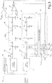
Figure 1 shows a general block diagram of a memory device of a known type; -
Figure 2 shows a block diagram of a read-amplifier circuit of the memory device shown inFigure 1 , which is also of a known type; -
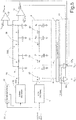
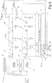
Figures 3 ,5 , and6 show general block diagrams of memory devices, parts of these devices being shown in terms of equivalent electrical circuits; and -
Figure 4 shows time plots of electrical quantities generated in the memory device shown inFigure 3 . - The present memory device and the present reading method stem from an observation made by the present Applicant, who has noted how, when a row of a memory device is selected, the corresponding memory cells are not pre-charged simultaneously, on account of inevitable propagation delays.
- In greater detail, with reference for example to a memory device of a flash type such as the one shown in
Figures 1 and 2 , each word line WL is formed by the gate terminals of thememory cells 3 coupled thereto and is typically provided with a metal layer having a high resistance. Moreover, the gate terminals of the floating-gate transistors form a system of capacitors connected to the word line WL. Consequently, each word line WL may be considered equivalent to a series of RC elements. For these reasons, the gate terminals of the floating-gate transistors of thememory cells 3 coupled to a word line WL selected are charged in times that increase the greater their distance from the row-decoder circuit 5. - This being said, a first embodiment of the present memory device is now described in detail, with reference to
Figure 3 , where the present memory device is designated by 20, and where components already present in the device shown inFigures 1 and 2 are designated by the same terms and references, except where otherwise specified. - Without any loss of generality, the
memory device 20 is thus of a non-volatile flash type. Moreover, in what follows thememory device 20 is described with reference to the differences with respect to the device shown inFigures 1 and 2 . In addition, inFigure 3 thememory cells 3 are represented with equivalent electrical models. - More in particular, in
Figure 3 thememory cells 3 coupled to each word line WL (only one of which is shown inFigure 3 ) are grouped in sets ofcells 23, each of which is formed by a same number ofmemory cells 3 arranged in sequence. Without any loss of generality, the sets ofcells 23 have a same value of resistance and a same value of capacitance. In addition, each set ofcells 23 is represented by a resistor R and by a capacitor C. In particular, given a set ofcells 23, a first terminal of the respective resistor R is designed to be connected to the second terminal of the resistor R of the previous set of cells, whereas a second terminal of the respective resistor R is designed to be connected to a first terminal of the respective capacitor C, the second terminal of which is connected to ground. - By way of example, appearing in
Figure 3 are a first internal node, a second internal node, an (N-1)-th internal node, and an N-th internal node, which are designated, respectively, by N1, N2, NN-1, and NN. The first internal node N1 and the N-th internal node NN are, respectively, the node that is closest to and the node that is furthest away from the row-decoder circuit 5. Once again without any loss of generality, it is, for example, possible to have N = 200 and thus each set ofcells 23 is formed by two hundredmemory cells 3, which are such that the resistance of the resistor R and the capacitance of the capacitor C are 50 kΩ and 4 pF, respectively. In this case, considering the high number ofmemory cells 3 coupled to each word line WL, thememory device 20 forms a so-called memory of a stand-alone type. - This being said,
Figure 4 shows, in addition to an enable signal present at input to the row-decoder circuit 5, the plots of the voltages present on the gate terminals of the floating-gate transistors of twomemory cells 3 that are coupled to a same word line WL and that are, respectively, the one closest to and the one furthest away from the row-decoder circuit 5. In other words,Figure 4 shows the plot of the voltage of the gate terminal closest to the row-decoder circuit 5, as well as the plot of the voltage of the N-th internal node NN, i.e., the plot of the voltage of the gate terminal furthest away from the row-decoder circuit 5. - Once again with reference to
Figure 4 , it is assumed therein that the supply voltage Vdd is 5 V. In addition, it is assumed that amemory cell 3 is correctly pre-charged by the row-decoder circuit 5 when the gate terminal of its floating-gate transistor has reached 4.5 V. This being said, it is found that thememory cell 3 closest to the row-decoder circuit 5 is pre-charged approximately 5 ns after the aforementioned enable signal has enabled the row-decoder circuit 5, causing application to the word line WL, by the row-decoder circuit 5 itself, of a row-biasing voltage. Thememory cell 3 furthest away from the row-decoder circuit 5 is, instead, pre-charged after approximately 220 ns. This being said, as described in detail hereinafter, in thepresent memory device 20 reading is carried out without waiting 220 ns, i.e., without waiting for all thememory cells 3 of the word line WL to be pre-charged. - Once again with reference to
Figure 3 , for simplicity of representation it shows just a first bit line, a second bit line, and a third bit line, designated by BL1, BL2, and BL3, respectively, the positions of which with respect to the series of RC elements that form the word line WL shown inFigure 3 are purely indicative, since, as has been said, each set ofcells 23 comprises a high number of memory cells and is represented only as equivalent electrical circuit. In this connection, with reference to the word line WL shown inFigure 3 , the first and second bit lines BL1, BL2 are coupled to the first set ofcells 23, i.e., to the set ofcells 23 closest to the row-decoder circuit 5, the second bit line BL2 being set at a greater distance from the latter than the first bit line BL1; the third bit line is, instead, coupled to the second set ofcells 23. Coupling between the first, second, and third bit lines BL1, BL2, and BL3 and the corresponding sets ofcells 23 occurs in a per se known manner and is shown only qualitatively inFigure 3 , where the portions of the first, second, and third bit lines BL1, BL2, BL3 within thememory array 2 are represented dashed, to indicate that they are purely qualitative. In practice, since each set ofcells 23 includes a number N ofmemory cells 3,Figure 3 does not indicate precisely to whichmemory cells 3 of the word line WL the first, second, and third bit lines BL1, BL2, BL3 are coupled, but rather merely provides, in this connection, qualitative information. In particular,Figure 3 highlights how, with reference to the single row of thememory array 2 shown, the first and second bit lines BL1, BL2 are coupled tomemory cells 3 belonging to the first set ofcells 23, whereas the third bit line BL3 is coupled to amemory cell 3 belonging to the second set ofcells 23. - As regards the read-
amplifier circuit 10, it is represented in order to highlight the presence of a first sense amplifier SA1, a second sense amplifier SA2, and a third sense amplifier SA3, which receive at input a reading reference voltage Vrif_read and may be coupled, respectively, through the column-decoder circuit 4, to the first, second, and third bit lines BL1, BL2, BL3. Further reference amplifiers, which may be coupled to the other bit lines (not shown) of thememory array 2, are not represented. - In a per se known manner, the first and second sense amplifiers SA1, SA2 are provided with respective enable inputs designed to receive a first sense-enable signal SAenable1, which has the purpose of enabling/disabling operation of these sense amplifiers. In turn, the third sense amplifier SA3 is provided with a respective enable input designed to receive a second sense-enable signal SAenable2, which has the purpose of enabling/disabling operation of this sense amplifier. Moreover, when enabled, the first, second, and third sense amplifiers SA1, SA2, SA3 are designed to generate, respectively, a first digital reading signal Sout1, a second digital reading signal Sout2, and a third digital reading signal Sout3.
- As shown once again in
Figure 3 , thememory device 20 further comprises adummy structure 30, asynchronisation circuit 32, and afirst comparison circuit 34 and asecond comparison circuit 35. In turn, thedummy structure 30 comprises adummy decoder 36 and adummy row 38. - In detail, the
dummy row 38 is the same as one of the rows (which are the same as one another) of thememory array 2, and is thus formed bymemory cells 3, which will be referred to in what follows also as "dummy memory cells". Moreover, thedummy structure 30 comprises a respective dummy word line WLD. The dummy memory cells are coupled to the dummy word line WLD and to corresponding bit lines BL of the memory array 2 (the latter connections are not visible inFigure 3 ). In this regard,Figure 3 shows the equivalent circuit models of sets ofdummy cells 23D, these sets being the same as the sets ofcells 23 of thememory array 2. - The
dummy decoder 36 is designed to select, i.e., to pre-charge, thedummy row 38. Moreover, thedummy decoder 36 simulates the behaviour of the row-decoder circuit 5; consequently, thedummy decoder 36 is, for example, the same as the row-decoder circuit 5. - In greater detail, the
dummy decoder 36 is driven by thesynchronisation circuit 32, which in turn receives at input the same signals as the ones that are received at input by the row-decoder circuit 5, so that thesynchronisation circuit 32 is designed to detect the presence of a new address, as well as start of a new read cycle. - In use, at each read cycle the
synchronisation circuit 32 drives thedummy decoder 36 so that the row-decoder circuit 5 and thedummy decoder 36 pre-charge simultaneously, respectively, the row to be read of thememory array 2 and thedummy row 38. In other words, the row-decoder circuit 5 and thedummy decoder 36 apply simultaneously a same row-biasing voltage to the word line WL of the row to be read of thememory array 2 and to the dummy word line WLD, respectively. Since the dummy word line WLD is the same as the word line WL of thememory array 2, the evolution in time of the voltage along the dummy word line WLD is the same as the evolution of the voltage along the word line WL of the row to be read. - The
first comparison circuit 34 has a first input set at a comparison reference voltage Vrif_comp; moreover, thefirst comparison circuit 34 has a second input, which is connected to a gate terminal of one of the floating-gate transistors that forms one of the dummy memory cells, which will be referred to in what follows as "comparison node Nc". For the reasons explained previously, and thus on account of the electrical model adopted for the sets ofdummy cells 23D, inFigure 3 the position of the comparison node Nc is purely qualitative and may not be identified with the corresponding electrical node shown inFigure 3 . For this reason, the connection between the comparison node Nc and thefirst comparison circuit 34 is represented dashed. - As regards the position of the comparison node Nc along the
dummy row 38, it separates thedummy row 38 into a first portion, connected to thedummy decoder 36, and a second portion, set downstream of the first portion. Likewise, each row of thememory array 2 may be viewed as being made up of a respective first portion, that is the same as the first portion of thedummy row 38, and a respective second portion, that is the same as the second portion of thedummy row 38. In addition, the row-decoder circuit 5 and the first and second portions of each row of thememory array 2 have the same mutual arrangement as thedummy decoder 36 and the first and second portions of thedummy row 38. - From yet another point of view, in each word line WL of the
memory array 2 there exists a gate terminal of one of the floating-gate transistors that forms a node (not shown) arranged, within the corresponding row of thememory array 2, in the same position as that assumed by the comparison node Nc within thedummy row 38. In what follows, this node will be referred to as "equivalent node". The first portion of each row of thememory array 2 includes, as last cell, the memory cell that forms the respective equivalent node. - In yet other words, the comparison node Nc is formed by a dummy cell having a given position, different from the last position, within the
dummy row 38. The first portion of each row of thememory array 2 includes thememory cells 3 that have, within the respective row, positions comprised between the first position and the position itself of the dummy cell that forms the comparison node Nc. The second portion of each row of thememory array 2 includes, instead, thememory cells 3 that have, within the respective row, positions comprised between the position subsequent to the position of the dummy cell that forms the comparison node Nc and the last position. - On the basis of what has been said previously, the evolution of the voltage of each equivalent node follows that of the voltage on the comparison node Nc. Purely by way of example, in the embodiment shown in
Figure 3 , the first and second bit lines BL1, BL2 are arranged upstream of the equivalent nodes of the rows of thememory array 2; i.e., they are coupled tomemory cells 3 that are arranged, for each row, closer to the row-decoder circuit 5 than thememory cell 3 the floating-gate transistor of which forms the corresponding equivalent node. The third bit line BL3 is arranged downstream of the equivalent nodes of the rows of thememory array 2. - The comparison reference voltage Vrif_comp is equal to the value of voltage that enables correct pre-charging of the
memory cells 3, i.e., for enabling reading thereof. For example, with reference toFigure 4 , the comparison reference voltage Vrif_comp is 4.5 Volt. - The
comparison circuit 34 generates the aforementioned first sense-enable signal SAenable1 as a function of the comparison reference voltage Vrif_comp and of the voltage of the comparison node Nc so that the first sense-enable signal SAenable1 represents the relation existing between these two signals. - As mentioned previously, the first sense-enable signal SAenable1 is supplied on the enable inputs of the first and second sense amplifiers SA1, SA2, and more in general on the enable inputs of the sense amplifiers that may be coupled to bit lines arranged upstream with respect to the equivalent nodes, or else to the bit line coupled to the equivalent nodes.
- In detail, the
first comparison circuit 34 detects overstepping, by the voltage of the comparison node Nc, of the comparison reference voltage Vrif_comp. - In greater detail, the
first comparison circuit 34 generates the first sense-enable signal SAenable1 so that, when the voltage of the comparison node Nc exceeds the comparison reference voltage Vrif_comp, the first sense-enable signal SAenable1 enables operation of the sense amplifiers that may be coupled to bit lines coupled to the first portions of the rows of thememory array 2. For example, with reference to just the first, second, and third sense amplifiers SA1, SA2, SA3, when the voltage of the comparison node Nc exceeds the comparison reference voltage Vrif_comp, just the first and second sense amplifiers SA1, SA2 are enabled. - The sense amplifiers that may be coupled to bit lines coupled to the second portions of the rows of the
memory array 2 are, instead, enabled subsequently, as described in what follows. - In detail, as mentioned previously, the second sense-enable signal SAenable2 is supplied on the enable input of the third sense amplifier SA3; more in general, the second sense-enable signal SAenable2 is supplied on the enable inputs of the sense amplifiers that may be coupled to bit lines arranged downstream with respect to the equivalent nodes so as to bring about enabling thereof.
- In greater detail, the second sense-enable signal SAenable2 is generated by the
second comparison circuit 35, which has a first input set at the comparison reference voltage Vrif_comp. Moreover, thesecond comparison circuit 35 has a second input, which is connected to the gate terminal of the floating-gate transistor that forms the last memory cell of thedummy row 38. - Yet in greater detail, the
second comparison circuit 35 generates the second sense-enable signal SAenable2 as a function of the comparison reference voltage Vrif_comp and of the voltage present on the gate terminal of the floating-gate transistor that forms the last memory cell of thedummy row 38, so that the second sense-enable signal SAenable2 represents the relation existing between these two signals. - In use, the
second comparison circuit 35 detects overstepping, by the voltage present on the gate terminal of the floating-gate transistor that forms the last memory cell of thedummy row 38, of the comparison reference voltage Vrif_comp. In particular, thesecond comparison circuit 35 generates the second sense-enable signal SAenable2 so that, when the voltage present on the gate terminal of the floating-gate transistor that forms the last memory cell of thedummy row 38 exceeds the comparison reference voltage Vrif_comp, the second sense-enable signal SAenable2 enables operation of the sense amplifiers that may be coupled to bit lines BL coupled to the second portions of the rows of thememory array 2. For example, with reference to just the first, second, and third sense amplifiers SA1, SA2, SA3, when the voltage present on the gate terminal of the floating-gate transistor that forms the last memory cell of thedummy row 38 exceeds the comparison reference voltage Vrif_comp, just the third sense amplifier SA3 is enabled. - In practice, given a row selected, the
memory device 20 envisages reading of the data items stored in the first portion of this row selected as soon as the entire first portion is correctly pre-charged, without waiting for all thememory cells 3 of the row selected to be correctly pre-charged. The data items of the second portion of the row selected are read subsequently, when all thememory cells 3 of the row selected have been correctly pre-charged. In this way, the initial latency is markedly reduced. - This being said, to clarify the behaviour of the
memory device 20, it is assumed that the delay due to the reading circuitry is 10 ns, and that it is desired to obtain an initial latency of 20 ns, as against 220 ns. It is moreover assumed that there apply the curves shown inFigure 4 , and that the comparison node Nc is formed by the gate terminal of the first floating-gate transistor of the seventh set ofdummy cells 23D. It is moreover assumed that the comparison node Nc takes 20 ns to reach the comparison reference voltage Vrif_comp, starting from when thedummy decoder 36 applies the row-biasing voltage to the dummy word line WLD. In addition, it is assumed that, as mentioned previously, each set ofcells 23 is formed by two hundred cells, and thus that six sets ofcells 23 comprise one thousand two hundredmemory cells 3, i.e., 150 bytes. - This being said, after 30 ns, the
memory device 20 makes available the digital output signals corresponding to the data items stored in thememory cells 3 of the first portion of the row selected. Consequently, after 30 ns the first 150 bytes are ready to be transmitted on a bus (not shown). On the hypothesis of transmitting at 200 MHz and with an output parallelism of eight, to transmit the first 150 bytes, 750 ns are necessary. Consequently, once transmission is through, also the second portion of the row selected is correctly pre-charged, and thus also the remaining data items, stored in the second portion of the row selected, are available and may be transmitted. Thus, the initial latency is equal to 30 ns. Moreover, recalling that thelast memory cell 3 of the row selected is correctly pre-charged after 220 ns, we obtain that the minimum time of transmission of a single byte is 200 ns / 150 bytes = 1.33 ns; consequently, the maximum value admissible of transmission frequency is 750 MHz. In this case, it is found that, when the first 150 bytes have been transmitted, it is possible to start transmission of the bytes corresponding to the second portion of the row selected. - Once again with reference to the embodiment shown in
Figure 3 , the corresponding structure may be better understood with reference toFigure 5 , where it is assumed that each set ofcells 23 of thememory array 2 is formed by asingle memory cell 3, as likewise each set ofcells 23D of thedummy row 38. Consequently, the couplings shown inFigure 5 between the RC elements and the other elements of thememory device 20 may be interpreted quantitatively because each RC element corresponds to asingle memory cell 3. We thus have, for example, that the internal nodes N1, N2, NN-1, NN coincide, respectively, with the gate terminals of the floating-gate transistors that form the first, second, (N-1)-th, and N-th memory cell 3 of the row of thememory array 2 shown inFigure 5 . Moreover, we have that the comparison node Nc coincides with the gate terminal of the floating-gate transistor that forms the first memory cell of thedummy row 38. Again, the first and second sense amplifiers SA1, SA2 are adjacent and receive at input, respectively, the first and second sense-enable signals SAenable1, SAenable2. Moreover, the first and second bit lines BL1, BL2 are coupled, respectively, to the first andsecond memory cells 3 of each row of thememory array 2, these last couplings being shown qualitatively, the electrical equivalents of the conduction terminals of the floating-gate transistors not being shown. The third sense amplifier SA3 is no longer represented. - According to a different embodiment (not shown), the number of
memory cells 3 that form each row of thememory array 2 may be smaller than the one referred to previously; for example, this number may be two thousand and forty-eight. The memory device may thus form a so-called embedded memory. In this case, it is, for example, possible for the first andlast memory cells 3 of each between thedummy row 38 and the rows of thememory array 2 to be pre-charged correctly after 2.07 ns and 3.6 ns, respectively. Thus, assuming again that each set ofcells 23 is formed by two hundredmemory cells 3 and assuming, for example, that the last memory cell of the seventh set ofcells 23 coincides with the comparison node Nc and is pre-charged correctly after 2.6 ns, it is possible to reduce the initial latency from 3.6 ns to 2.6 ns. This reduction of the initial latency, albeit limited in absolute value, is in any case important in relative terms. -
Figure 6 shows a further embodiment, which differs from the embodiment shown inFigure 3 in that it further comprises aboost circuit 41, of a per se known type. Without any loss of generality, it is moreover assumed that the number ofmemory cells 3 for each row is two thousand and forty-eight. - The
boost circuit 41 is driven by thesynchronisation circuit 32 in a way synchronous with thedummy decoder 36. Moreover, theboost circuit 41 is operatively coupled to thedummy decoder 36 and to the row-decoder circuit 5. - The
boost circuit 41 includes a respective capacitor (not shown), which is charged before the read cycles, and is subsequently coupled to the dummy word line WLD and to the word line WL selected, when thedummy decoder 36 and the row-decoder circuit 5 start to pre-charge, so as to impose a fast variation of the row-biasing voltage. - In practice, the
boost circuit 41 enables charging of both the dummy word line WLD and of each of the word lines WL in a faster way than what would occur in the absence of theboost circuit 41, without resorting to a row-decoder circuit having a lower resistance. - In general, the
boost circuit 41 may be used also in the case of a high number ofmemory cells 3 per row. - The advantages of the solution proposed emerge clearly from the foregoing description. In particular, the present memory device enables reading of the data items set in an initial portion of each row as soon as the cells of this initial portion are correctly pre-charged, without waiting for the entire row to be correctly pre-charged, thus reducing the initial latency. In this connection, reading is not completely random; in fact, the data items set in the initial portion of each row exhibit a lower latency than the data items set in the subsequent portion. This fact may be taken into consideration during storage of the data items.
- Finally, it is clear that modifications and variations may be made to what has been described and illustrated herein, without thereby departing from the scope of the present invention, as defined in the annexed claims.
- In particular, it is emphasized how the reading method implemented by the embodiments described previously may be applied also in the case of memory devices of a different type, such as the so-called PCMs. More in general, the present reading method may be implemented in all the memories with array arrangement of the cells, which inevitably suffer from propagation delays.
- Moreover, it is possible for more than one comparison node to be present in the dummy row, all the comparison nodes being connected to a comparison stage, which generates sense-enable signals so that they indicate instants of time in which the comparison nodes reach the comparison reference voltage Vrif_comp. In practice, in the presence of a number X of comparison nodes, each row of the
memory array 2 is divided into X+1 consecutive portions. Given a row selected for reading, assuming an index "i" for indexing the first X portions of the row selected, the data items stored in the i-th portion are made available when i-th comparison node has reached the comparison reference voltage Vrif_comp; the data items corresponding to the last portion are made available after the last cell of the row selected has been pre-charged. In this way, it is possible to reduce the initial latency even further. - Irrespective of the embodiment adopted, one or more cells of each row may contain bits corresponding to a check code, such as a parity-check code, for reducing any possible errors of reading of the proper data items.
Claims (10)
- A memory device comprising:- a memory array (2) including a plurality of memory cells (3) arranged in rows and columns and a plurality of word lines (WL) and bit lines (BL);- a dummy structure (30) comprising a dummy row (38) of dummy cells and a dummy word line (WLD);- a first pre-charging stage (5) configured to bias, in a step of pre-charging of an operation of reading of said memory array, a word line of said memory array;- an output stage (4, 10, 34, 35) comprising a plurality of sense amplifiers (SA1, SA2, SA3), each sense amplifier being couplable in an electrically controlled way to a corresponding bit line during said reading operation and configured to generate a corresponding output signal representing a data item stored in a corresponding memory cell coupled to said corresponding bit line and pre-charged by said first pre-charging stage; and- a second pre-charging stage (32, 36) configured to bias the dummy word line simultaneously with the word line biased by the first pre-charging stage;and wherein said output stage comprises a first sense-enable stage (34), which is configured to detect a state of complete pre-charging of at least one dummy cell intermediate between the dummy cells of the dummy row; and wherein a first part of said sense amplifiers (SA1, SA2) is configured to generate the corresponding output signals following upon sensing of said state of complete pre-charging of the intermediate dummy cell.
- The memory device according to claim 1, wherein said output stage (4, 10, 34, 35) further comprises a second sense-enable stage (35), which is configured to detect a state of complete pre-charging of the last dummy cell of the dummy row (38); and wherein a second part of said sense amplifiers (SA3) is configured to generate the corresponding output signals following upon sensing of said state of complete pre-charging of the last dummy cell of the dummy row.
- The memory device according to claim 1 or claim 2, wherein said at least one intermediate dummy cell has a respective position within the dummy row (38); and wherein said first part of said sense amplifiers (SA1, SA2) may be coupled to bit lines (BL1, BL2) coupled to memory cells (3) that have positions, within the respective rows, comprised between the first position and the position of the intermediate dummy cell.
- The memory device according to claim 3, when depending upon claim 2, wherein said second part of said sense amplifiers (SA3) may be coupled to bit lines (BL3) that are coupled to memory cells (3) that have positions, within the respective rows, comprised between the position subsequent to the position of the intermediate dummy cell and the last position.
- The memory device according to any one of the preceding claims, further comprising a boost circuit (41) of a capacitive type, which is configured to charge in a synchronous way the dummy row (38) and the word line (WL) biased by the first pre-charging stage (5).
- A method for reading a memory device (20) comprising:- a memory array (2) including a plurality of memory cells (3) arranged in rows and columns and a plurality of word lines (WL) and bit lines (BL);- a dummy structure (30) comprising a dummy row (38) of dummy cells and a dummy word line (WLD);- a pre-charging stage (5) configured to bias, in a step of pre-charging of an operation of reading of said memory array, a word line of said memory array; and- an output stage (4, 10, 34, 35) comprising a plurality of sense amplifiers (SA1, SA2, SA3), each sense amplifier being couplable in an electrically controlled way to a corresponding bit line during said reading operation and configured to generate a corresponding output signal representing a data item stored in a corresponding memory cell coupled to said corresponding bit line and pre-charged by said pre-charging stage;said method comprising the steps of:- biasing the dummy word line simultaneously with the word line biased by the first pre-charging stage;- detecting a state of complete pre-charging of at least one dummy cell intermediate between the dummy cells of the dummy row; and- by a first part of said sense amplifiers (SA1, SA2), generating corresponding output signals following upon sensing of said state of complete pre-charging of the intermediate dummy cell.
- The reading method according to claim 6, further comprising the steps of:- detecting a state of complete pre-charging of the last dummy cell of the dummy row (38);- by a second part of said sense amplifiers (SA3), generating corresponding output signals following upon sensing of said state of complete pre-charging of the last dummy cell of the dummy row.
- The reading method according to claim 6 or claim 7, wherein said at least one intermediate dummy cell has a respective position within the dummy row (38); and wherein said first part of said sense amplifiers (SA1, SA2) may be coupled to bit lines (BL1, BL2) coupled to memory cells (3) that have positions, within the respective rows, comprised between the first position and the position of the intermediate dummy cell.
- The reading method according to claim 8, when depending upon claim 7, wherein said second part of said sense amplifiers (SA3) may be coupled to bit lines (BL3) coupled to memory cells (3) that have positions, within the respective rows, comprised between the position subsequent to the position of the intermediate dummy cell and the last position.
- The reading method according to any one of claims 6 to 9, further comprising the step of charging synchronously the dummy row (38) and the word line (WL) biased by the pre-charging stage (5), by a boost circuit (41) of a capacitive type.
Applications Claiming Priority (1)
| Application Number | Priority Date | Filing Date | Title |
|---|---|---|---|
| ITUA2016A003999A ITUA20163999A1 (en) | 2016-05-31 | 2016-05-31 | MEMORY DEVICE WITH PROGRESSIVE READING OF THE LINE AND ITS READING METHOD |
Publications (2)
| Publication Number | Publication Date |
|---|---|
| EP3252776A1 true EP3252776A1 (en) | 2017-12-06 |
| EP3252776B1 EP3252776B1 (en) | 2020-03-18 |
Family
ID=56940295
Family Applications (1)
| Application Number | Title | Priority Date | Filing Date |
|---|---|---|---|
| EP16206895.1A Active EP3252776B1 (en) | 2016-05-31 | 2016-12-23 | Memory device with progressive row reading and related reading method |
Country Status (3)
| Country | Link |
|---|---|
| US (2) | US9805810B1 (en) |
| EP (1) | EP3252776B1 (en) |
| IT (1) | ITUA20163999A1 (en) |
Families Citing this family (2)
| Publication number | Priority date | Publication date | Assignee | Title |
|---|---|---|---|---|
| DE112019007383B4 (en) * | 2019-05-31 | 2026-05-13 | Micron Technology, Inc. | METHOD FOR VERIFYING THE ERASE PHASE OF A STORAGE DEVICE |
| FR3146541A1 (en) * | 2023-03-07 | 2024-09-13 | Stmicroelectronics International N.V. | Method of reading a memory |
Citations (3)
| Publication number | Priority date | Publication date | Assignee | Title |
|---|---|---|---|---|
| US20030086304A1 (en) * | 2001-11-02 | 2003-05-08 | Jong-Hun Park | Semiconductor memory device |
| US20100290295A1 (en) * | 2009-05-12 | 2010-11-18 | Fujitsu Semiconductor Limited | Semiconductor memory and system |
| US20110158029A1 (en) * | 2009-12-25 | 2011-06-30 | Kabushiki Kaisha Toshiba | Word line driving circuit and semiconductor storage device |
Family Cites Families (5)
| Publication number | Priority date | Publication date | Assignee | Title |
|---|---|---|---|---|
| JP3548423B2 (en) * | 1998-04-27 | 2004-07-28 | シャープ株式会社 | Semiconductor storage device |
| JP4804133B2 (en) * | 2005-12-06 | 2011-11-02 | ルネサスエレクトロニクス株式会社 | Nonvolatile semiconductor memory device |
| US7613055B2 (en) * | 2007-08-09 | 2009-11-03 | Altera Corporation | Programmable control block for dual port SRAM application |
| US8767494B2 (en) * | 2012-06-11 | 2014-07-01 | Taiwan Semiconductor Manufacturing Co., Ltd. | Far end resistance tracking design with near end pre-charge control for faster recovery time |
| CN105190760B (en) * | 2012-11-12 | 2018-04-24 | 马维尔国际贸易有限公司 | Concurrently using the sram cell for passing through both doors by door and PMOS with NMOS in accumulator system |
-
2016
- 2016-05-31 IT ITUA2016A003999A patent/ITUA20163999A1/en unknown
- 2016-12-21 US US15/387,397 patent/US9805810B1/en active Active
- 2016-12-23 EP EP16206895.1A patent/EP3252776B1/en active Active
-
2017
- 2017-10-27 US US15/795,552 patent/US10002672B2/en active Active
Patent Citations (3)
| Publication number | Priority date | Publication date | Assignee | Title |
|---|---|---|---|---|
| US20030086304A1 (en) * | 2001-11-02 | 2003-05-08 | Jong-Hun Park | Semiconductor memory device |
| US20100290295A1 (en) * | 2009-05-12 | 2010-11-18 | Fujitsu Semiconductor Limited | Semiconductor memory and system |
| US20110158029A1 (en) * | 2009-12-25 | 2011-06-30 | Kabushiki Kaisha Toshiba | Word line driving circuit and semiconductor storage device |
Also Published As
| Publication number | Publication date |
|---|---|
| US9805810B1 (en) | 2017-10-31 |
| ITUA20163999A1 (en) | 2017-12-01 |
| US20180047455A1 (en) | 2018-02-15 |
| EP3252776B1 (en) | 2020-03-18 |
| US10002672B2 (en) | 2018-06-19 |
Similar Documents
| Publication | Publication Date | Title |
|---|---|---|
| TWI569276B (en) | One time programmable non-volatile memory and associated read sensing method | |
| US5729492A (en) | Sense amplifier having capacitively coupled input for offset compensation | |
| US7952958B2 (en) | Non-volatile semiconductor storage system | |
| CN107180652B (en) | Circuit and method for reading memory cells of a non-volatile memory device | |
| US10803931B2 (en) | Non-volatile memory having memory array with differential cells | |
| CN108538334B (en) | One-time programmable non-volatile memory and read sensing method thereof | |
| US8908430B2 (en) | Semiconductor device and method of operating the same | |
| TWI734582B (en) | Non-volatile memory and associated write verification method | |
| JP2020532040A5 (en) | ||
| CN111370044B (en) | Semiconductor device | |
| US9589608B2 (en) | Semiconductor memory device | |
| US10811102B2 (en) | Flash memory storage apparatus and reading method thereof | |
| US8804438B2 (en) | Memory device | |
| JP2014086111A (en) | Semiconductor device | |
| US8687423B2 (en) | Nonvolatile memory device and method of operating the same | |
| US10002672B2 (en) | Memory device with progressive row reading and related reading method | |
| US9691499B1 (en) | Semiconductor memory device | |
| US8547751B2 (en) | Non-volatile storage device | |
| JPH07320493A (en) | Integrated circuit memory with improved access time | |
| US6826112B2 (en) | Low power logic gate | |
| CN110349602B (en) | Actively-configured memory reading device, memory and electronic equipment | |
| US20040141393A1 (en) | Method and apparatus for selecting memory cells within a memory array | |
| US7813196B2 (en) | Integrated semiconductor memory and method for operating a data path in a semiconductor memory | |
| US7489555B2 (en) | Program-verify sensing for a multi-level cell (MLC) flash memory device | |
| WO2007015097A1 (en) | Memory bitcell and method of using the same |
Legal Events
| Date | Code | Title | Description |
|---|---|---|---|
| PUAI | Public reference made under article 153(3) epc to a published international application that has entered the european phase |
Free format text: ORIGINAL CODE: 0009012 |
|
| STAA | Information on the status of an ep patent application or granted ep patent |
Free format text: STATUS: THE APPLICATION HAS BEEN PUBLISHED |
|
| AK | Designated contracting states |
Kind code of ref document: A1 Designated state(s): AL AT BE BG CH CY CZ DE DK EE ES FI FR GB GR HR HU IE IS IT LI LT LU LV MC MK MT NL NO PL PT RO RS SE SI SK SM TR |
|
| AX | Request for extension of the european patent |
Extension state: BA ME |
|
| STAA | Information on the status of an ep patent application or granted ep patent |
Free format text: STATUS: REQUEST FOR EXAMINATION WAS MADE |
|
| 17P | Request for examination filed |
Effective date: 20180605 |
|
| RBV | Designated contracting states (corrected) |
Designated state(s): AL AT BE BG CH CY CZ DE DK EE ES FI FR GB GR HR HU IE IS IT LI LT LU LV MC MK MT NL NO PL PT RO RS SE SI SK SM TR |
|
| STAA | Information on the status of an ep patent application or granted ep patent |
Free format text: STATUS: EXAMINATION IS IN PROGRESS |
|
| 17Q | First examination report despatched |
Effective date: 20190130 |
|
| RIC1 | Information provided on ipc code assigned before grant |
Ipc: G11C 7/14 20060101ALI20190802BHEP Ipc: G11C 16/28 20060101ALI20190802BHEP Ipc: G11C 7/06 20060101ALN20190802BHEP Ipc: G11C 7/22 20060101ALI20190802BHEP Ipc: G11C 8/14 20060101ALI20190802BHEP Ipc: G11C 16/24 20060101ALN20190802BHEP Ipc: G11C 16/26 20060101ALI20190802BHEP Ipc: G11C 16/08 20060101ALI20190802BHEP Ipc: G11C 16/32 20060101ALI20190802BHEP Ipc: G11C 11/56 20060101ALI20190802BHEP Ipc: G11C 8/08 20060101AFI20190802BHEP |
|
| GRAP | Despatch of communication of intention to grant a patent |
Free format text: ORIGINAL CODE: EPIDOSNIGR1 |
|
| STAA | Information on the status of an ep patent application or granted ep patent |
Free format text: STATUS: GRANT OF PATENT IS INTENDED |
|
| INTG | Intention to grant announced |
Effective date: 20191007 |
|
| GRAS | Grant fee paid |
Free format text: ORIGINAL CODE: EPIDOSNIGR3 |
|
| GRAA | (expected) grant |
Free format text: ORIGINAL CODE: 0009210 |
|
| STAA | Information on the status of an ep patent application or granted ep patent |
Free format text: STATUS: THE PATENT HAS BEEN GRANTED |
|
| RIN1 | Information on inventor provided before grant (corrected) |
Inventor name: POLIZZI, SALVATORE Inventor name: CAMPARDO, GIOVANNI |
|
| AK | Designated contracting states |
Kind code of ref document: B1 Designated state(s): AL AT BE BG CH CY CZ DE DK EE ES FI FR GB GR HR HU IE IS IT LI LT LU LV MC MK MT NL NO PL PT RO RS SE SI SK SM TR |
|
| REG | Reference to a national code |
Ref country code: GB Ref legal event code: FG4D |
|
| REG | Reference to a national code |
Ref country code: DE Ref legal event code: R096 Ref document number: 602016031945 Country of ref document: DE |
|
| REG | Reference to a national code |
Ref country code: AT Ref legal event code: REF Ref document number: 1246844 Country of ref document: AT Kind code of ref document: T Effective date: 20200415 Ref country code: IE Ref legal event code: FG4D |
|
| PG25 | Lapsed in a contracting state [announced via postgrant information from national office to epo] |
Ref country code: RS Free format text: LAPSE BECAUSE OF FAILURE TO SUBMIT A TRANSLATION OF THE DESCRIPTION OR TO PAY THE FEE WITHIN THE PRESCRIBED TIME-LIMIT Effective date: 20200318 Ref country code: NO Free format text: LAPSE BECAUSE OF FAILURE TO SUBMIT A TRANSLATION OF THE DESCRIPTION OR TO PAY THE FEE WITHIN THE PRESCRIBED TIME-LIMIT Effective date: 20200618 Ref country code: FI Free format text: LAPSE BECAUSE OF FAILURE TO SUBMIT A TRANSLATION OF THE DESCRIPTION OR TO PAY THE FEE WITHIN THE PRESCRIBED TIME-LIMIT Effective date: 20200318 |
|
| REG | Reference to a national code |
Ref country code: NL Ref legal event code: MP Effective date: 20200318 |
|
| PG25 | Lapsed in a contracting state [announced via postgrant information from national office to epo] |
Ref country code: LV Free format text: LAPSE BECAUSE OF FAILURE TO SUBMIT A TRANSLATION OF THE DESCRIPTION OR TO PAY THE FEE WITHIN THE PRESCRIBED TIME-LIMIT Effective date: 20200318 Ref country code: SE Free format text: LAPSE BECAUSE OF FAILURE TO SUBMIT A TRANSLATION OF THE DESCRIPTION OR TO PAY THE FEE WITHIN THE PRESCRIBED TIME-LIMIT Effective date: 20200318 Ref country code: GR Free format text: LAPSE BECAUSE OF FAILURE TO SUBMIT A TRANSLATION OF THE DESCRIPTION OR TO PAY THE FEE WITHIN THE PRESCRIBED TIME-LIMIT Effective date: 20200619 Ref country code: HR Free format text: LAPSE BECAUSE OF FAILURE TO SUBMIT A TRANSLATION OF THE DESCRIPTION OR TO PAY THE FEE WITHIN THE PRESCRIBED TIME-LIMIT Effective date: 20200318 Ref country code: BG Free format text: LAPSE BECAUSE OF FAILURE TO SUBMIT A TRANSLATION OF THE DESCRIPTION OR TO PAY THE FEE WITHIN THE PRESCRIBED TIME-LIMIT Effective date: 20200618 |
|
| REG | Reference to a national code |
Ref country code: LT Ref legal event code: MG4D |
|
| PG25 | Lapsed in a contracting state [announced via postgrant information from national office to epo] |
Ref country code: NL Free format text: LAPSE BECAUSE OF FAILURE TO SUBMIT A TRANSLATION OF THE DESCRIPTION OR TO PAY THE FEE WITHIN THE PRESCRIBED TIME-LIMIT Effective date: 20200318 |
|
| PG25 | Lapsed in a contracting state [announced via postgrant information from national office to epo] |
Ref country code: SM Free format text: LAPSE BECAUSE OF FAILURE TO SUBMIT A TRANSLATION OF THE DESCRIPTION OR TO PAY THE FEE WITHIN THE PRESCRIBED TIME-LIMIT Effective date: 20200318 Ref country code: PT Free format text: LAPSE BECAUSE OF FAILURE TO SUBMIT A TRANSLATION OF THE DESCRIPTION OR TO PAY THE FEE WITHIN THE PRESCRIBED TIME-LIMIT Effective date: 20200812 Ref country code: EE Free format text: LAPSE BECAUSE OF FAILURE TO SUBMIT A TRANSLATION OF THE DESCRIPTION OR TO PAY THE FEE WITHIN THE PRESCRIBED TIME-LIMIT Effective date: 20200318 Ref country code: RO Free format text: LAPSE BECAUSE OF FAILURE TO SUBMIT A TRANSLATION OF THE DESCRIPTION OR TO PAY THE FEE WITHIN THE PRESCRIBED TIME-LIMIT Effective date: 20200318 Ref country code: CZ Free format text: LAPSE BECAUSE OF FAILURE TO SUBMIT A TRANSLATION OF THE DESCRIPTION OR TO PAY THE FEE WITHIN THE PRESCRIBED TIME-LIMIT Effective date: 20200318 Ref country code: IS Free format text: LAPSE BECAUSE OF FAILURE TO SUBMIT A TRANSLATION OF THE DESCRIPTION OR TO PAY THE FEE WITHIN THE PRESCRIBED TIME-LIMIT Effective date: 20200718 Ref country code: SK Free format text: LAPSE BECAUSE OF FAILURE TO SUBMIT A TRANSLATION OF THE DESCRIPTION OR TO PAY THE FEE WITHIN THE PRESCRIBED TIME-LIMIT Effective date: 20200318 Ref country code: LT Free format text: LAPSE BECAUSE OF FAILURE TO SUBMIT A TRANSLATION OF THE DESCRIPTION OR TO PAY THE FEE WITHIN THE PRESCRIBED TIME-LIMIT Effective date: 20200318 |
|
| REG | Reference to a national code |
Ref country code: AT Ref legal event code: MK05 Ref document number: 1246844 Country of ref document: AT Kind code of ref document: T Effective date: 20200318 |
|
| REG | Reference to a national code |
Ref country code: DE Ref legal event code: R097 Ref document number: 602016031945 Country of ref document: DE |
|
| PLBE | No opposition filed within time limit |
Free format text: ORIGINAL CODE: 0009261 |
|
| STAA | Information on the status of an ep patent application or granted ep patent |
Free format text: STATUS: NO OPPOSITION FILED WITHIN TIME LIMIT |
|
| PG25 | Lapsed in a contracting state [announced via postgrant information from national office to epo] |
Ref country code: IT Free format text: LAPSE BECAUSE OF FAILURE TO SUBMIT A TRANSLATION OF THE DESCRIPTION OR TO PAY THE FEE WITHIN THE PRESCRIBED TIME-LIMIT Effective date: 20200318 Ref country code: AT Free format text: LAPSE BECAUSE OF FAILURE TO SUBMIT A TRANSLATION OF THE DESCRIPTION OR TO PAY THE FEE WITHIN THE PRESCRIBED TIME-LIMIT Effective date: 20200318 Ref country code: DK Free format text: LAPSE BECAUSE OF FAILURE TO SUBMIT A TRANSLATION OF THE DESCRIPTION OR TO PAY THE FEE WITHIN THE PRESCRIBED TIME-LIMIT Effective date: 20200318 Ref country code: ES Free format text: LAPSE BECAUSE OF FAILURE TO SUBMIT A TRANSLATION OF THE DESCRIPTION OR TO PAY THE FEE WITHIN THE PRESCRIBED TIME-LIMIT Effective date: 20200318 |
|
| 26N | No opposition filed |
Effective date: 20201221 |
|
| PG25 | Lapsed in a contracting state [announced via postgrant information from national office to epo] |
Ref country code: PL Free format text: LAPSE BECAUSE OF FAILURE TO SUBMIT A TRANSLATION OF THE DESCRIPTION OR TO PAY THE FEE WITHIN THE PRESCRIBED TIME-LIMIT Effective date: 20200318 |
|
| PG25 | Lapsed in a contracting state [announced via postgrant information from national office to epo] |
Ref country code: SI Free format text: LAPSE BECAUSE OF FAILURE TO SUBMIT A TRANSLATION OF THE DESCRIPTION OR TO PAY THE FEE WITHIN THE PRESCRIBED TIME-LIMIT Effective date: 20200318 |
|
| REG | Reference to a national code |
Ref country code: CH Ref legal event code: PL |
|
| GBPC | Gb: european patent ceased through non-payment of renewal fee |
Effective date: 20201223 |
|
| PG25 | Lapsed in a contracting state [announced via postgrant information from national office to epo] |
Ref country code: MC Free format text: LAPSE BECAUSE OF FAILURE TO SUBMIT A TRANSLATION OF THE DESCRIPTION OR TO PAY THE FEE WITHIN THE PRESCRIBED TIME-LIMIT Effective date: 20200318 |
|
| REG | Reference to a national code |
Ref country code: BE Ref legal event code: MM Effective date: 20201231 |
|
| PG25 | Lapsed in a contracting state [announced via postgrant information from national office to epo] |
Ref country code: IE Free format text: LAPSE BECAUSE OF NON-PAYMENT OF DUE FEES Effective date: 20201223 Ref country code: LU Free format text: LAPSE BECAUSE OF NON-PAYMENT OF DUE FEES Effective date: 20201223 Ref country code: FR Free format text: LAPSE BECAUSE OF NON-PAYMENT OF DUE FEES Effective date: 20201231 |
|
| PG25 | Lapsed in a contracting state [announced via postgrant information from national office to epo] |
Ref country code: CH Free format text: LAPSE BECAUSE OF NON-PAYMENT OF DUE FEES Effective date: 20201231 Ref country code: LI Free format text: LAPSE BECAUSE OF NON-PAYMENT OF DUE FEES Effective date: 20201231 Ref country code: GB Free format text: LAPSE BECAUSE OF NON-PAYMENT OF DUE FEES Effective date: 20201223 |
|
| PG25 | Lapsed in a contracting state [announced via postgrant information from national office to epo] |
Ref country code: TR Free format text: LAPSE BECAUSE OF FAILURE TO SUBMIT A TRANSLATION OF THE DESCRIPTION OR TO PAY THE FEE WITHIN THE PRESCRIBED TIME-LIMIT Effective date: 20200318 Ref country code: MT Free format text: LAPSE BECAUSE OF FAILURE TO SUBMIT A TRANSLATION OF THE DESCRIPTION OR TO PAY THE FEE WITHIN THE PRESCRIBED TIME-LIMIT Effective date: 20200318 Ref country code: CY Free format text: LAPSE BECAUSE OF FAILURE TO SUBMIT A TRANSLATION OF THE DESCRIPTION OR TO PAY THE FEE WITHIN THE PRESCRIBED TIME-LIMIT Effective date: 20200318 |
|
| PG25 | Lapsed in a contracting state [announced via postgrant information from national office to epo] |
Ref country code: MK Free format text: LAPSE BECAUSE OF FAILURE TO SUBMIT A TRANSLATION OF THE DESCRIPTION OR TO PAY THE FEE WITHIN THE PRESCRIBED TIME-LIMIT Effective date: 20200318 Ref country code: AL Free format text: LAPSE BECAUSE OF FAILURE TO SUBMIT A TRANSLATION OF THE DESCRIPTION OR TO PAY THE FEE WITHIN THE PRESCRIBED TIME-LIMIT Effective date: 20200318 |
|
| PG25 | Lapsed in a contracting state [announced via postgrant information from national office to epo] |
Ref country code: BE Free format text: LAPSE BECAUSE OF NON-PAYMENT OF DUE FEES Effective date: 20201231 |
|
| PGFP | Annual fee paid to national office [announced via postgrant information from national office to epo] |
Ref country code: DE Payment date: 20251126 Year of fee payment: 10 |