EP3252528A2 - Liquid crystal display and manufacturing method thereof - Google Patents
Liquid crystal display and manufacturing method thereof Download PDFInfo
- Publication number
- EP3252528A2 EP3252528A2 EP17174112.7A EP17174112A EP3252528A2 EP 3252528 A2 EP3252528 A2 EP 3252528A2 EP 17174112 A EP17174112 A EP 17174112A EP 3252528 A2 EP3252528 A2 EP 3252528A2
- Authority
- EP
- European Patent Office
- Prior art keywords
- liquid crystal
- alignment layer
- layer
- substrate
- group
- Prior art date
- Legal status (The legal status is an assumption and is not a legal conclusion. Google has not performed a legal analysis and makes no representation as to the accuracy of the status listed.)
- Granted
Links
Images



Classifications
-
- G—PHYSICS
- G02—OPTICS
- G02F—OPTICAL DEVICES OR ARRANGEMENTS FOR THE CONTROL OF LIGHT BY MODIFICATION OF THE OPTICAL PROPERTIES OF THE MEDIA OF THE ELEMENTS INVOLVED THEREIN; NON-LINEAR OPTICS; FREQUENCY-CHANGING OF LIGHT; OPTICAL LOGIC ELEMENTS; OPTICAL ANALOGUE/DIGITAL CONVERTERS
- G02F1/00—Devices or arrangements for the control of the intensity, colour, phase, polarisation or direction of light arriving from an independent light source, e.g. switching, gating or modulating; Non-linear optics
- G02F1/01—Devices or arrangements for the control of the intensity, colour, phase, polarisation or direction of light arriving from an independent light source, e.g. switching, gating or modulating; Non-linear optics for the control of the intensity, phase, polarisation or colour
- G02F1/13—Devices or arrangements for the control of the intensity, colour, phase, polarisation or direction of light arriving from an independent light source, e.g. switching, gating or modulating; Non-linear optics for the control of the intensity, phase, polarisation or colour based on liquid crystals, e.g. single liquid crystal display cells
- G02F1/133—Constructional arrangements; Operation of liquid crystal cells; Circuit arrangements
- G02F1/1333—Constructional arrangements; Manufacturing methods
- G02F1/1337—Surface-induced orientation of the liquid crystal molecules, e.g. by alignment layers
- G02F1/133711—Surface-induced orientation of the liquid crystal molecules, e.g. by alignment layers by organic films, e.g. polymeric films
-
- C—CHEMISTRY; METALLURGY
- C09—DYES; PAINTS; POLISHES; NATURAL RESINS; ADHESIVES; COMPOSITIONS NOT OTHERWISE PROVIDED FOR; APPLICATIONS OF MATERIALS NOT OTHERWISE PROVIDED FOR
- C09K—MATERIALS FOR MISCELLANEOUS APPLICATIONS, NOT PROVIDED FOR ELSEWHERE
- C09K19/00—Liquid crystal materials
- C09K19/52—Liquid crystal materials characterised by components which are not liquid crystals, e.g. additives with special physical aspect: solvents, solid particles
- C09K19/54—Additives having no specific mesophase characterised by their chemical composition
-
- C—CHEMISTRY; METALLURGY
- C08—ORGANIC MACROMOLECULAR COMPOUNDS; THEIR PREPARATION OR CHEMICAL WORKING-UP; COMPOSITIONS BASED THEREON
- C08F—MACROMOLECULAR COMPOUNDS OBTAINED BY REACTIONS ONLY INVOLVING CARBON-TO-CARBON UNSATURATED BONDS
- C08F22/00—Homopolymers and copolymers of compounds having one or more unsaturated aliphatic radicals each having only one carbon-to-carbon double bond, and at least one being terminated by a carboxyl radical and containing at least one other carboxyl radical in the molecule; Salts, anhydrides, esters, amides, imides or nitriles thereof
- C08F22/10—Esters
- C08F22/1006—Esters of polyhydric alcohols or polyhydric phenols, e.g. ethylene glycol dimethacrylate
-
- C—CHEMISTRY; METALLURGY
- C09—DYES; PAINTS; POLISHES; NATURAL RESINS; ADHESIVES; COMPOSITIONS NOT OTHERWISE PROVIDED FOR; APPLICATIONS OF MATERIALS NOT OTHERWISE PROVIDED FOR
- C09K—MATERIALS FOR MISCELLANEOUS APPLICATIONS, NOT PROVIDED FOR ELSEWHERE
- C09K19/00—Liquid crystal materials
- C09K19/04—Liquid crystal materials characterised by the chemical structure of the liquid crystal components, e.g. by a specific unit
- C09K19/38—Polymers
- C09K19/3833—Polymers with mesogenic groups in the side chain
- C09K19/3842—Polyvinyl derivatives
- C09K19/3852—Poly(meth)acrylate derivatives
-
- C—CHEMISTRY; METALLURGY
- C09—DYES; PAINTS; POLISHES; NATURAL RESINS; ADHESIVES; COMPOSITIONS NOT OTHERWISE PROVIDED FOR; APPLICATIONS OF MATERIALS NOT OTHERWISE PROVIDED FOR
- C09K—MATERIALS FOR MISCELLANEOUS APPLICATIONS, NOT PROVIDED FOR ELSEWHERE
- C09K19/00—Liquid crystal materials
- C09K19/04—Liquid crystal materials characterised by the chemical structure of the liquid crystal components, e.g. by a specific unit
- C09K19/38—Polymers
- C09K19/3833—Polymers with mesogenic groups in the side chain
- C09K19/3842—Polyvinyl derivatives
- C09K19/3852—Poly(meth)acrylate derivatives
- C09K19/3857—Poly(meth)acrylate derivatives containing at least one asymmetric carbon atom
-
- C—CHEMISTRY; METALLURGY
- C09—DYES; PAINTS; POLISHES; NATURAL RESINS; ADHESIVES; COMPOSITIONS NOT OTHERWISE PROVIDED FOR; APPLICATIONS OF MATERIALS NOT OTHERWISE PROVIDED FOR
- C09K—MATERIALS FOR MISCELLANEOUS APPLICATIONS, NOT PROVIDED FOR ELSEWHERE
- C09K19/00—Liquid crystal materials
- C09K19/52—Liquid crystal materials characterised by components which are not liquid crystals, e.g. additives with special physical aspect: solvents, solid particles
- C09K19/54—Additives having no specific mesophase characterised by their chemical composition
- C09K19/56—Aligning agents
-
- G—PHYSICS
- G02—OPTICS
- G02F—OPTICAL DEVICES OR ARRANGEMENTS FOR THE CONTROL OF LIGHT BY MODIFICATION OF THE OPTICAL PROPERTIES OF THE MEDIA OF THE ELEMENTS INVOLVED THEREIN; NON-LINEAR OPTICS; FREQUENCY-CHANGING OF LIGHT; OPTICAL LOGIC ELEMENTS; OPTICAL ANALOGUE/DIGITAL CONVERTERS
- G02F1/00—Devices or arrangements for the control of the intensity, colour, phase, polarisation or direction of light arriving from an independent light source, e.g. switching, gating or modulating; Non-linear optics
- G02F1/01—Devices or arrangements for the control of the intensity, colour, phase, polarisation or direction of light arriving from an independent light source, e.g. switching, gating or modulating; Non-linear optics for the control of the intensity, phase, polarisation or colour
- G02F1/13—Devices or arrangements for the control of the intensity, colour, phase, polarisation or direction of light arriving from an independent light source, e.g. switching, gating or modulating; Non-linear optics for the control of the intensity, phase, polarisation or colour based on liquid crystals, e.g. single liquid crystal display cells
- G02F1/133—Constructional arrangements; Operation of liquid crystal cells; Circuit arrangements
- G02F1/1333—Constructional arrangements; Manufacturing methods
- G02F1/1337—Surface-induced orientation of the liquid crystal molecules, e.g. by alignment layers
-
- G—PHYSICS
- G02—OPTICS
- G02F—OPTICAL DEVICES OR ARRANGEMENTS FOR THE CONTROL OF LIGHT BY MODIFICATION OF THE OPTICAL PROPERTIES OF THE MEDIA OF THE ELEMENTS INVOLVED THEREIN; NON-LINEAR OPTICS; FREQUENCY-CHANGING OF LIGHT; OPTICAL LOGIC ELEMENTS; OPTICAL ANALOGUE/DIGITAL CONVERTERS
- G02F1/00—Devices or arrangements for the control of the intensity, colour, phase, polarisation or direction of light arriving from an independent light source, e.g. switching, gating or modulating; Non-linear optics
- G02F1/01—Devices or arrangements for the control of the intensity, colour, phase, polarisation or direction of light arriving from an independent light source, e.g. switching, gating or modulating; Non-linear optics for the control of the intensity, phase, polarisation or colour
- G02F1/13—Devices or arrangements for the control of the intensity, colour, phase, polarisation or direction of light arriving from an independent light source, e.g. switching, gating or modulating; Non-linear optics for the control of the intensity, phase, polarisation or colour based on liquid crystals, e.g. single liquid crystal display cells
- G02F1/133—Constructional arrangements; Operation of liquid crystal cells; Circuit arrangements
- G02F1/1333—Constructional arrangements; Manufacturing methods
- G02F1/1337—Surface-induced orientation of the liquid crystal molecules, e.g. by alignment layers
- G02F1/133707—Structures for producing distorted electric fields, e.g. bumps, protrusions, recesses, slits in pixel electrodes
-
- G—PHYSICS
- G02—OPTICS
- G02F—OPTICAL DEVICES OR ARRANGEMENTS FOR THE CONTROL OF LIGHT BY MODIFICATION OF THE OPTICAL PROPERTIES OF THE MEDIA OF THE ELEMENTS INVOLVED THEREIN; NON-LINEAR OPTICS; FREQUENCY-CHANGING OF LIGHT; OPTICAL LOGIC ELEMENTS; OPTICAL ANALOGUE/DIGITAL CONVERTERS
- G02F1/00—Devices or arrangements for the control of the intensity, colour, phase, polarisation or direction of light arriving from an independent light source, e.g. switching, gating or modulating; Non-linear optics
- G02F1/01—Devices or arrangements for the control of the intensity, colour, phase, polarisation or direction of light arriving from an independent light source, e.g. switching, gating or modulating; Non-linear optics for the control of the intensity, phase, polarisation or colour
- G02F1/13—Devices or arrangements for the control of the intensity, colour, phase, polarisation or direction of light arriving from an independent light source, e.g. switching, gating or modulating; Non-linear optics for the control of the intensity, phase, polarisation or colour based on liquid crystals, e.g. single liquid crystal display cells
- G02F1/133—Constructional arrangements; Operation of liquid crystal cells; Circuit arrangements
- G02F1/1333—Constructional arrangements; Manufacturing methods
- G02F1/1337—Surface-induced orientation of the liquid crystal molecules, e.g. by alignment layers
- G02F1/133711—Surface-induced orientation of the liquid crystal molecules, e.g. by alignment layers by organic films, e.g. polymeric films
- G02F1/133726—Surface-induced orientation of the liquid crystal molecules, e.g. by alignment layers by organic films, e.g. polymeric films made of a mesogenic material
-
- G—PHYSICS
- G02—OPTICS
- G02F—OPTICAL DEVICES OR ARRANGEMENTS FOR THE CONTROL OF LIGHT BY MODIFICATION OF THE OPTICAL PROPERTIES OF THE MEDIA OF THE ELEMENTS INVOLVED THEREIN; NON-LINEAR OPTICS; FREQUENCY-CHANGING OF LIGHT; OPTICAL LOGIC ELEMENTS; OPTICAL ANALOGUE/DIGITAL CONVERTERS
- G02F1/00—Devices or arrangements for the control of the intensity, colour, phase, polarisation or direction of light arriving from an independent light source, e.g. switching, gating or modulating; Non-linear optics
- G02F1/01—Devices or arrangements for the control of the intensity, colour, phase, polarisation or direction of light arriving from an independent light source, e.g. switching, gating or modulating; Non-linear optics for the control of the intensity, phase, polarisation or colour
- G02F1/13—Devices or arrangements for the control of the intensity, colour, phase, polarisation or direction of light arriving from an independent light source, e.g. switching, gating or modulating; Non-linear optics for the control of the intensity, phase, polarisation or colour based on liquid crystals, e.g. single liquid crystal display cells
- G02F1/133—Constructional arrangements; Operation of liquid crystal cells; Circuit arrangements
- G02F1/1333—Constructional arrangements; Manufacturing methods
- G02F1/1337—Surface-induced orientation of the liquid crystal molecules, e.g. by alignment layers
- G02F1/133753—Surface-induced orientation of the liquid crystal molecules, e.g. by alignment layers with different alignment orientations or pretilt angles on a same surface, e.g. for grey scale or improved viewing angle
-
- G—PHYSICS
- G02—OPTICS
- G02F—OPTICAL DEVICES OR ARRANGEMENTS FOR THE CONTROL OF LIGHT BY MODIFICATION OF THE OPTICAL PROPERTIES OF THE MEDIA OF THE ELEMENTS INVOLVED THEREIN; NON-LINEAR OPTICS; FREQUENCY-CHANGING OF LIGHT; OPTICAL LOGIC ELEMENTS; OPTICAL ANALOGUE/DIGITAL CONVERTERS
- G02F1/00—Devices or arrangements for the control of the intensity, colour, phase, polarisation or direction of light arriving from an independent light source, e.g. switching, gating or modulating; Non-linear optics
- G02F1/01—Devices or arrangements for the control of the intensity, colour, phase, polarisation or direction of light arriving from an independent light source, e.g. switching, gating or modulating; Non-linear optics for the control of the intensity, phase, polarisation or colour
- G02F1/13—Devices or arrangements for the control of the intensity, colour, phase, polarisation or direction of light arriving from an independent light source, e.g. switching, gating or modulating; Non-linear optics for the control of the intensity, phase, polarisation or colour based on liquid crystals, e.g. single liquid crystal display cells
- G02F1/133—Constructional arrangements; Operation of liquid crystal cells; Circuit arrangements
- G02F1/1333—Constructional arrangements; Manufacturing methods
- G02F1/1337—Surface-induced orientation of the liquid crystal molecules, e.g. by alignment layers
- G02F1/13378—Surface-induced orientation of the liquid crystal molecules, e.g. by alignment layers by treatment of the surface, e.g. embossing, rubbing or light irradiation
- G02F1/133788—Surface-induced orientation of the liquid crystal molecules, e.g. by alignment layers by treatment of the surface, e.g. embossing, rubbing or light irradiation by light irradiation, e.g. linearly polarised light photo-polymerisation
-
- G—PHYSICS
- G02—OPTICS
- G02F—OPTICAL DEVICES OR ARRANGEMENTS FOR THE CONTROL OF LIGHT BY MODIFICATION OF THE OPTICAL PROPERTIES OF THE MEDIA OF THE ELEMENTS INVOLVED THEREIN; NON-LINEAR OPTICS; FREQUENCY-CHANGING OF LIGHT; OPTICAL LOGIC ELEMENTS; OPTICAL ANALOGUE/DIGITAL CONVERTERS
- G02F1/00—Devices or arrangements for the control of the intensity, colour, phase, polarisation or direction of light arriving from an independent light source, e.g. switching, gating or modulating; Non-linear optics
- G02F1/01—Devices or arrangements for the control of the intensity, colour, phase, polarisation or direction of light arriving from an independent light source, e.g. switching, gating or modulating; Non-linear optics for the control of the intensity, phase, polarisation or colour
- G02F1/13—Devices or arrangements for the control of the intensity, colour, phase, polarisation or direction of light arriving from an independent light source, e.g. switching, gating or modulating; Non-linear optics for the control of the intensity, phase, polarisation or colour based on liquid crystals, e.g. single liquid crystal display cells
- G02F1/133—Constructional arrangements; Operation of liquid crystal cells; Circuit arrangements
- G02F1/1333—Constructional arrangements; Manufacturing methods
- G02F1/1343—Electrodes
- G02F1/134309—Electrodes characterised by their geometrical arrangement
-
- G—PHYSICS
- G02—OPTICS
- G02F—OPTICAL DEVICES OR ARRANGEMENTS FOR THE CONTROL OF LIGHT BY MODIFICATION OF THE OPTICAL PROPERTIES OF THE MEDIA OF THE ELEMENTS INVOLVED THEREIN; NON-LINEAR OPTICS; FREQUENCY-CHANGING OF LIGHT; OPTICAL LOGIC ELEMENTS; OPTICAL ANALOGUE/DIGITAL CONVERTERS
- G02F1/00—Devices or arrangements for the control of the intensity, colour, phase, polarisation or direction of light arriving from an independent light source, e.g. switching, gating or modulating; Non-linear optics
- G02F1/01—Devices or arrangements for the control of the intensity, colour, phase, polarisation or direction of light arriving from an independent light source, e.g. switching, gating or modulating; Non-linear optics for the control of the intensity, phase, polarisation or colour
- G02F1/13—Devices or arrangements for the control of the intensity, colour, phase, polarisation or direction of light arriving from an independent light source, e.g. switching, gating or modulating; Non-linear optics for the control of the intensity, phase, polarisation or colour based on liquid crystals, e.g. single liquid crystal display cells
- G02F1/133—Constructional arrangements; Operation of liquid crystal cells; Circuit arrangements
- G02F1/136—Liquid crystal cells structurally associated with a semi-conducting layer or substrate, e.g. cells forming part of an integrated circuit
- G02F1/1362—Active matrix addressed cells
- G02F1/1368—Active matrix addressed cells in which the switching element is a three-electrode device
-
- C—CHEMISTRY; METALLURGY
- C09—DYES; PAINTS; POLISHES; NATURAL RESINS; ADHESIVES; COMPOSITIONS NOT OTHERWISE PROVIDED FOR; APPLICATIONS OF MATERIALS NOT OTHERWISE PROVIDED FOR
- C09K—MATERIALS FOR MISCELLANEOUS APPLICATIONS, NOT PROVIDED FOR ELSEWHERE
- C09K19/00—Liquid crystal materials
- C09K19/52—Liquid crystal materials characterised by components which are not liquid crystals, e.g. additives with special physical aspect: solvents, solid particles
- C09K2019/523—Organic solid particles
-
- C—CHEMISTRY; METALLURGY
- C09—DYES; PAINTS; POLISHES; NATURAL RESINS; ADHESIVES; COMPOSITIONS NOT OTHERWISE PROVIDED FOR; APPLICATIONS OF MATERIALS NOT OTHERWISE PROVIDED FOR
- C09K—MATERIALS FOR MISCELLANEOUS APPLICATIONS, NOT PROVIDED FOR ELSEWHERE
- C09K2323/00—Functional layers of liquid crystal optical display excluding electroactive liquid crystal layer characterised by chemical composition
- C09K2323/02—Alignment layer characterised by chemical composition
-
- G—PHYSICS
- G02—OPTICS
- G02F—OPTICAL DEVICES OR ARRANGEMENTS FOR THE CONTROL OF LIGHT BY MODIFICATION OF THE OPTICAL PROPERTIES OF THE MEDIA OF THE ELEMENTS INVOLVED THEREIN; NON-LINEAR OPTICS; FREQUENCY-CHANGING OF LIGHT; OPTICAL LOGIC ELEMENTS; OPTICAL ANALOGUE/DIGITAL CONVERTERS
- G02F1/00—Devices or arrangements for the control of the intensity, colour, phase, polarisation or direction of light arriving from an independent light source, e.g. switching, gating or modulating; Non-linear optics
- G02F1/01—Devices or arrangements for the control of the intensity, colour, phase, polarisation or direction of light arriving from an independent light source, e.g. switching, gating or modulating; Non-linear optics for the control of the intensity, phase, polarisation or colour
- G02F1/13—Devices or arrangements for the control of the intensity, colour, phase, polarisation or direction of light arriving from an independent light source, e.g. switching, gating or modulating; Non-linear optics for the control of the intensity, phase, polarisation or colour based on liquid crystals, e.g. single liquid crystal display cells
- G02F1/133—Constructional arrangements; Operation of liquid crystal cells; Circuit arrangements
- G02F1/1333—Constructional arrangements; Manufacturing methods
- G02F1/1337—Surface-induced orientation of the liquid crystal molecules, e.g. by alignment layers
- G02F1/133753—Surface-induced orientation of the liquid crystal molecules, e.g. by alignment layers with different alignment orientations or pretilt angles on a same surface, e.g. for grey scale or improved viewing angle
- G02F1/133761—Surface-induced orientation of the liquid crystal molecules, e.g. by alignment layers with different alignment orientations or pretilt angles on a same surface, e.g. for grey scale or improved viewing angle with different pretilt angles
-
- G—PHYSICS
- G02—OPTICS
- G02F—OPTICAL DEVICES OR ARRANGEMENTS FOR THE CONTROL OF LIGHT BY MODIFICATION OF THE OPTICAL PROPERTIES OF THE MEDIA OF THE ELEMENTS INVOLVED THEREIN; NON-LINEAR OPTICS; FREQUENCY-CHANGING OF LIGHT; OPTICAL LOGIC ELEMENTS; OPTICAL ANALOGUE/DIGITAL CONVERTERS
- G02F2201/00—Constructional arrangements not provided for in groups G02F1/00 - G02F7/00
- G02F2201/12—Constructional arrangements not provided for in groups G02F1/00 - G02F7/00 electrode
- G02F2201/121—Constructional arrangements not provided for in groups G02F1/00 - G02F7/00 electrode common or background
-
- G—PHYSICS
- G02—OPTICS
- G02F—OPTICAL DEVICES OR ARRANGEMENTS FOR THE CONTROL OF LIGHT BY MODIFICATION OF THE OPTICAL PROPERTIES OF THE MEDIA OF THE ELEMENTS INVOLVED THEREIN; NON-LINEAR OPTICS; FREQUENCY-CHANGING OF LIGHT; OPTICAL LOGIC ELEMENTS; OPTICAL ANALOGUE/DIGITAL CONVERTERS
- G02F2201/00—Constructional arrangements not provided for in groups G02F1/00 - G02F7/00
- G02F2201/12—Constructional arrangements not provided for in groups G02F1/00 - G02F7/00 electrode
- G02F2201/123—Constructional arrangements not provided for in groups G02F1/00 - G02F7/00 electrode pixel
Definitions
- the present invention relates to a liquid crystal display and a manufacturing method thereof.
- a liquid crystal display includes a display panel including field generating electrodes such as a pixel electrode and a common electrode, and a liquid crystal layer formed in an electric field generated by the field generating electrodes.
- the liquid crystal display forms the electric field to the liquid crystal layer, thereby displaying an image by determining an arrangement of liquid crystal molecules included in the liquid crystal layer and controlling transmittance of a light passing through the liquid crystal layer.
- One aspect of the present invention is directed to a liquid crystal display, including a first substrate; a second substrate overlapping the first substrate; a liquid crystal layer positioned between the first substrate and the second substrate and including a plurality of liquid crystal molecules; a first alignment layer positioned between the first substrate and the liquid crystal layer; a second alignment layer positioned between the second substrate and the liquid crystal layer; and a plurality of protrusions positioned at at least one of between the first alignment layer and the liquid crystal layer and between the second alignment layer and the liquid crystal layer, wherein at least one among the plurality of protrusions includes a polymer of a reactive mesogen, and the reactive mesogen is represented by Chemical Formula 1.
- P a and P b are independently an acrylate group or a methacrylate group
- a 1 includes in which at least one hydrogen connected to a carbon ring is unsubstituted or substituted with one selected from a group including F, Cl, and Br
- a 2 includes any one of and in which at least one hydrogen connected to the carbon ring is unsubstituted or substituted with one selected from the group including F, Cl, and Br, and
- the first alignment layer may include a first polymer, the first polymer may include a first main chain and a plurality of first side chains connected to the first main chain, and at least one among the plurality of first side chains may include at least one of a photoreactive group and a photoreactive group derivative.
- the photoreactive group derivative included in the plurality of first side chains may be combined with the polymer of the reactive mesogen included in the plurality of protrusions.
- the second alignment layer may include a second polymer, the second polymer includes a second main chain and a plurality of second side chains connected to the second main chain, and the plurality of second side chains do not include the photo reactive group and the photoreactive group derivative.
- the reactive mesogen may be represented by Chemical Formula A or Chemical Formula B.
- P a and P b are independently the acrylate group or the methacrylate group, S is one selected from a group including F, Cl, and Br, x is 0, 1, 2, or 3, and n is the natural number of 2 to 5.
- the reactive mesogen may have heat resistance of 250 degrees Celsius or more.
- the density of the protrusions positioned between the first alignment layer and the liquid crystal layer may be higher than the density of the protrusions positioned between the second alignment layer and the liquid crystal layer among the plurality of protrusions.
- the pre-tilt angle of the liquid crystal molecules adjacent to the first alignment layer among the plurality of liquid crystal molecules may be larger than the pre-tilt angle of the liquid crystal molecules adjacent to the second alignment layer among the plurality of liquid crystal molecules.
- the first substrate and the second substrate may have a curved surface.
- the liquid crystal display may further include: a thin film transistor positioned between the first substrate and the first alignment layer; a pixel electrode connected to the thin film transistor; and a common electrode forming an electric field with the pixel electrode.
- the first alignment layer may include a lower alignment layer, an upper alignment layer, and a buffer region positioned between the lower alignment layer and the upper alignment layer, the upper alignment layer may include at least one of the photoreactive group and the photoreactive group derivative, the lower alignment layer may not include the photoreactive group and the photoreactive group derivative, and the buffer region may include less of the photoreactive group than the content of at least one of the photoreactive group and the photoreactive group derivative of the upper alignment layer.
- the size of the protrusions positioned between the first alignment layer and the liquid crystal layer may be smaller than the size of the protrusions positioned between the second alignment layer and the liquid crystal layer.
- Another aspect of the present invention is directed to a manufacturing method of a liquid crystal display, including preparing a lower panel including a first alignment layer positioned on a first substrate; preparing an upper panel including a second alignment layer positioned on a second substrate; forming a liquid crystal layer positioned between the lower panel and the upper panel and including a plurality of liquid crystal molecules; heat-treating the upper panel and the lower panel; and irradiating light to the lower panel, the upper panel, and the liquid crystal layer in a state in which an electric field is applied to the liquid crystal layer, and in the step of the heat treatment, a reactive mesogen included in at least one of the first alignment layer and the second alignment layer is adsorbed into the liquid crystal layer, in the light irradiation step, the reactive mesogen is polymerized to form a plurality of protrusions, and the reactive mesogen is represented by Chemical Formula 1.
- P a and P b are independently an acrylate group or a methacrylate group
- a 1 includes in which at least one hydrogen connected to a carbon ring is unsubstituted or substituted with one selected from a group including F, Cl, and Br
- a 2 includes any one of and in which at least one hydrogen connected to the carbon ring is unsubstituted or substituted with one selected from the group including F, Cl, and Br
- n is a natural number of 2 to 5.
- the first alignment layer may include a first polymer, the first polymer may include a first main chain and a plurality of first side chains connected to the first main chain, and at least one among the plurality of first side chains may include a photoreactive group.
- the second alignment layer may include a second polymer, the second polymer may include a second main chain and a plurality of second side chains connected to the second main chain, and the plurality of second side chains may not include the photoreactive group.
- the reactive mesogen may be represented by Chemical Formula A or Chemical Formula B.
- P a and P b are independently the acrylate group or the methacrylate group, S is one selected from a group including F, Cl, and Br, x is 0, 1, 2, or 3, and n is the natural number of 2 to 5.
- the density of the plurality of protrusions positioned between the first alignment layer and the liquid crystal layer may be larger than the density of the plurality of protrusions positioned between the second alignment layer and the liquid crystal layer.
- the density of the protrusions positioned between the first alignment layer and the liquid crystal layer may be higher than the density of the protrusions positioned between the second alignment layer and the liquid crystal layer.
- the pre-tilt angle of the liquid crystal molecules adjacent to the first alignment layer among the plurality of liquid crystal molecules may be larger than the pre-tilt angle of the liquid crystal molecules adjacent to the second alignment layer among the plurality of liquid crystal molecules.
- the manufacturing method of the liquid crystal display may further include providing a curved surface to the first substrate and the second substrate.
- the first alignment layer may be divided into a lower alignment layer and an upper alignment layer, a buffer region is formed between the lower alignment layer and the upper alignment layer, the upper alignment layer may include the photoreactive group, the lower alignment layer may not include the photoreactive group, and the buffer region may include less of the photoreactive group than the content of the photoreactive group distributed in the upper alignment layer.
- the manufacturing method may be used to manufacture a liquid crystal display described herein.
- a liquid crystal display including a first substrate, a second substrate facing the first substrate, a liquid crystal layer between the first substrate and the second substrate, and an alignment layer between the first substrate and the second substrate and adjacent to the liquid crystal layer, the alignment layer having protruding polymeric structures, the polymeric structures being coupled to the material of the alignment layer via a (meth)acrylate moiety, the polymeric structures including a polymer unit having a first moiety that is a divalent biphenyl moiety, a diether linkage in which two oxygens are joined by a carbon chain of 2 to 5 carbons, and a second moiety that is a divalent phenyl or biphenyl moiety, wherein the first and second moieties are connected by the diether linkage.
- the polymer unit may be represented by Chemical Formula 2: wherein, in Chemical Formula 2, A 1 is the first moiety, A 2 is the second moiety, and n is a natural number of 2 to 5.
- a 1 may include and A 2 may include or
- At least one hydrogen connected to a carbon ring may be substituted with F, Cl, or Br.
- At least one hydrogen connected to a carbon ring may be substituted with F, Cl, or Br.
- the phrase “on a flat surface” means when an object portion is viewed from above, and the phrase “on a cross-section” means when a cross-section taken by vertically cutting an object portion is viewed from the side.
- FIG. 1 is a cross-sectional view showing a liquid crystal display according to an embodiment.
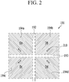
- FIG. 2 is a schematic top plan view showing a pixel electrode structure of FIG. 1 .
- the liquid crystal display according to the present embodiment includes a lower panel 100 and an upper panel 200 overlapping each other, and a liquid crystal layer 3 interposed between the two display panels 100 and 200.
- the lower panel 100 includes a first alignment layer 11 positioned at one side facing the liquid crystal layer 3, and the upper panel 200 includes a second alignment layer 21 positioned at one side facing the liquid crystal layer 3.
- a plurality of protrusions 15 and 25 are respectively positioned between the first alignment layer 11 and the liquid crystal layer 3 and between the second alignment layer 21 and the liquid crystal layer 3.
- At least one of the plurality of protrusions 15 and 25 includes a polymer of a reactive mesogen, and the reactive mesogen may be represented by Chemical Formula 1.
- P a and P b are (meth)acrylate terminal moieties, and are each independently an acrylate group or a methacrylate group.
- a 1 includes a divalent biphenyl moiety
- hydrogen connected to a carbon ring may be unsubstituted or substituted, for example, with F, Cl, or Br.
- a 2 includes a divalent moiety
- hydrogen connected to the carbon ring may be unsubstituted or substituted with, for example, F, Cl, or Br.
- the n is a natural number of 2 to 5.
- carbon ring indicates carbons connected to each other to form a ring.
- Chemical Formula 1 when a component to be polymerized like the acrylate group or the methacrylate group receives ultraviolet rays, a crosslinking reaction is generated such that the polymer may be formed.
- the reactive mesogen may be polymerized within itself such that the plurality of protrusions 15 and 25 may be formed. Also, the reactive mesogen may be combined with a photoreactive group included in a side chain of the alignment layers 11 and 21 described below.
- the reactive mesogen may have a three or four ring structure.
- a 1 has two ring structures
- a 2 may have one or two ring structures. Ring structures adjacent to each other are connected by a spacer such as -O-(CH 2 ) n O-.
- the reactive mesogen has heat resistance to more than about 250 degrees Celsius such that the reactivity may be small at less than the temperature.
- a length of a part that becomes a conjugation is elongated, and an ultraviolet ray absorption wavelength band may move into a long wavelength such that the reactivity for the ultraviolet rays may increase. If the reactivity substantially increases, most of the reactive mesogen may be polymerized and moves into the first alignment layer 11 or the second alignment layer 21 to decrease surface energy, thereby forming the protrusion. In this case, directivity in which the polymerized reactive mesogen moves to either alignment layer side of the first alignment layer 11 and the second alignment layer 21 may not be uniform. Accordingly, selectivity of liquid crystal molecules 310 respectively adjacent to the upper and lower panels 100 and 200 that have pre-tilts that are different from each other may be reduced.
- the reactive mesogen may have a spacer within the three or four ring structure, which may improve selectivity. Accordingly, the three or more ring structure may not be directly connected, and the length of the part that forms the conjugation may be reduced.
- the spacer includes an ether group (-O-) having stability (instead of, for example, an ester group (-COO-) included in the reactive mesogen represented by Chemical Formula X and Chemical Formula Y, below) such that the spacer portion may be prevented from being disconnected when irradiated with ultraviolet rays.
- an ether group (-O-) having stability instead of, for example, an ester group (-COO-) included in the reactive mesogen represented by Chemical Formula X and Chemical Formula Y, below
- the spacer includes an alkylene group in which a carbon number is 2 to 5.
- the solubility may increase. At the same time, a deformation may be more easily generated by an external stress, and the liquid crystal molecule 310 may not fully return to an initial position in a voltage off state. In such a case, an afterimage may be significant. If the length of the spacer is short, the solubility may be reduced. At this same time, rigidity may be increased, and afterimage may be reduced.
- the solubility means a degree that the reactive mesogen may be dissolved in the solvent of the alignment material. In the present embodiment, the carbon number of the alkylene group included in the spacer has the range of 2 to 5. In the present embodiment, an afterimage level that does not significantly affect the quality of the product may be maintained and the reactive mesogen may have solubility of a degree that it may be coated along with the alignment material by being dissolved in the solvent.
- the ring structure has a -C 6 H 4 C 6 H 4 - of a biphenylene structure, and the molecule structure may have a plane shape.
- an attraction force may be more easily generated between the molecules such that it tends to be easily crystallized. Accordingly, the solubility may be low.
- At least one hydrogen connected to the carbon ring may be substituted, for example, with F.
- a degree of crystallinity may be reduced by increasing a free volume.
- the free volume may mean an empty space around a configuration particle among a volume occupied with a material.
- F is the substituent.
- the reactive mesogen may be represented by Chemical Formula A or Chemical Formula B.
- P a and P b are independently an acrylate group or a methacrylate group
- S is one selected from a group including F, Cl, and Br
- x is 0, 1, 2, or 3
- n is a natural number of 2 to 5.
- the reactive mesogen represented by Chemical Formula B includes four ring structures.
- x may be 1 or more and/or n may be 2 or more.
- the reactive mesogen may include, for example, at least one among a group represented by Chemical Formula A-1 to Chemical Formula A-10.
- a reactive mesogen satisfying the structure of the above-described Chemical Formula A or Chemical Formula B may be included as well as those below.
- a plurality of gate lines are positioned on a first substrate 110.
- Each gate line includes a gate electrode 124 that is protruded from the gate line or a part of the gate line.
- a gate insulating layer 140 is positioned on the gate electrode 124, a semiconductor layer 154 is positioned on the gate insulating layer 140, and the semiconductor layer 154 overlaps the gate electrode 124.
- the semiconductor layer 154 may include amorphous silicon, polycrystalline silicon, or an oxide semiconductor.
- Ohmic contacts 163 and 165 may be positioned on the semiconductor layer 154.
- the ohmic contacts 163 and 165 may be formed of a material such as n+ hydrogenated amorphous silicon in which an n-type impurity is doped at a high concentration, or of a silicide.
- the ohmic contacts 163 and 165 may be omitted.
- a source electrode 173 and a drain electrode 175 are positioned on the ohmic contacts 163 and 165 and the gate insulating layer 140.
- a plurality of data lines may be positioned on the gate insulating layer 140, and each data line may be connected to a source electrode 173.
- the gate electrode 124, the source electrode 173, and the drain electrode 175 form a thin film transistor as a switching element along with the semiconductor layer 154.
- a first insulating layer 180a is positioned on the source electrode 173 and the drain electrode 175, and the first insulating layer 180a may be in contact with the semiconductor layer 154 in a separate space between the source electrode 173 and the drain electrode 175.
- the first insulating layer 180a may be made of the organic insulating material or the inorganic insulating material, and may include a single layer or a multilayer.
- a color filter 230 may be positioned on the first insulating layer 180a.
- the color filter 230 may display one of primary colors such as three primary colors of red, green, and blue, or the like.
- the color filter 230 may represent colors such as cyan, magenta, yellow, and a white-containing color.
- a second insulating layer 180b may be positioned on the color filter 230, and the second insulating layer 180b may include the inorganic insulating material or the organic insulating material.
- the second insulating layer 180b as an overcoat for the color filter 230, may be used to help prevent the color filter from being exposed outside and for realizing a flat surface.
- the second insulating layer 180b may be omitted.
- a pixel electrode 191 is positioned on the second insulating layer 180b, and the pixel electrode 191 is mainly positioned in a transmission region TA.
- the above-described gate line, data line, thin film transistor, and the like may be positioned in a light blocking region BA where light is not transmitted.
- the transmission region TA as a region where the image is mainly displayed is a region where the light may be transmitted, and the light blocking region BA is not a region for displaying the image and may be a region where the light may not be mainly transmitted.
- the first insulating layer 180a and the second insulating layer 180b have a contact hole 185, and the drain electrode 175 and the pixel electrode 191 are electrically connected to each other through the contact hole 185.
- the pixel electrode 191 includes a cross-shaped stem portion including a longitudinal stem portion 192 and a transverse stem portion 193 crossing the longitudinal stem portion 192. Also, the pixel electrode 191 is divided into a first sub-region Da, a second sub-region Db, a third sub-region Dc, and a fourth sub-region Dd by the longitudinal stem portion 192 and the transverse stem portion 193, and each sub-region includes a plurality of first to fourth fine branched portions 194a, 194b, 194c, and 194d.
- the first fine branched portion 194a extends obliquely in an upper left direction from the transverse stem portion 193 or the longitudinal stem portion 192
- the second fine branched portion 194b extends obliquely in an upper right direction from the transverse stem portion 193 or the longitudinal stem portion 192
- the third fine branched portion 194c extends obliquely in a lower left direction from the transverse stem portion 193 or the longitudinal stem portion 192
- the fourth fine branched portion 194d extends obliquely in a lower right direction from the transverse stem portion 193 or the longitudinal stem portion 192.
- the liquid crystal molecules 310 are inclined such that a long axis thereof is aligned in a direction perpendicular to a direction of an electric field by the electric field formed to the liquid crystal layer 3.
- the change degree of polarization of the light that is incident to the liquid crystal layer 3 is changed according to the inclination degree of the liquid crystal molecules 310, and this change of polarization appears as a change of transmittance by the polarizer, thereby displaying images of the liquid crystal display.
- a direction in which the liquid crystal molecule 310 is inclined is determined by the fine branched portions 194a, 194b, 194c, and 194d of the pixel electrode 191, and the liquid crystal molecule 310 is inclined toward a direction parallel with length directions of the fine branched portions 194a, 194b, 194c, and 194d.
- the one pixel electrode 191 includes four subregions Da, Db, Dc, and Dd in which the length directions of the fine branched portions 194a, 194b, 194c, and 194d are different from each other, and therefore directions in which the liquid crystal molecules 310 are inclined is approximately four directions.
- the liquid crystal layer 3 is formed with four domains in which the alignment directions of the liquid crystal molecules 310 are different.
- the direction in which the liquid crystal molecules are inclined varies, such that the viewing angle of the liquid crystal display may be improved.
- a light blocking member 220 is positioned on the second insulating layer 180b and the pixel electrode 191.
- the light blocking member 220 is positioned in the light blocking region BA.
- the light blocking member 220 is referred to as a black matrix.
- the light blocking member 220 includes a spacer 221 and a main light blocking portion 222.
- the main light blocking portion 222 to prevent light leakage is formed in the light blocking region BA positioned with the gate line, the data line, the thin film transistor, and the like, and the main light blocking portion 222 may have a substantially flat upper surface.
- the main light blocking portion 222 may overlap the contact hole 185.
- the main light blocking portion 222 overlapping the contact hole 185 fills the step generated in the contact hole 185, thereby flattening the surface and preventing light leakage therearound.
- the spacer 221 is connected to the main light blocking portion 222.
- the spacer 221 may be positioned on the signal line such as gate line and the data line, and/or the thin film transistor.
- the spacer 221 is separated from the upper panel 200, as an example variation, the spacer 221 and the upper panel 200 may be in contact.
- the spacer 221 serves to maintain a cell gap between the upper panel 200 and the lower panel 100. For example, when a distance between the upper panel 200 and the lower panel 100 becomes narrow by an external pressure against the liquid crystal display, it has a function of maintaining the cell gap between the upper panel 200 and the lower panel 100.
- the described content simultaneously forming the main light blocking portion 222 and the spacer 221 may be varied, and as an example variation, the main light blocking portion 222 and the spacer 221 may be separately formed.
- the first alignment layer 11 is positioned on the pixel electrode 191.
- the first alignment layer 11 includes a first polymer
- the first polymer includes a first main chain and a plurality of first side chains connected to the first main chain, and at least one among a plurality of first side chains may include one among a photoreactive group and a photoreactive group derivative.
- the photo reactive group derivative means a structure in which the photoreactive group irradiated with ultraviolet rays is chemically combined with the reactive mesogen to be modified.
- At least one among the plurality of first side chains may include a vertical alignment group.
- the photoreactive group may use various materials that may generate a radical by absorbing the light to initiate a polymerization reaction.
- the photoreactive group may include at least one among a group represented by Chemical Formula 1a to Chemical Formula 12a.
- the first alignment layer 11 may not include the photoreactive group or the photoreactive group derivative, and in this case, the plurality of protrusions 15 may also be formed in the surface of the first alignment layer 11 by the polymerization reaction of the reactive mesogen by ultraviolet rays.
- the common electrode 270 may be positioned between a second substrate 210 and the liquid crystal layer 3.
- the common electrode 270 may be formed as a whole plate on the entire surface of the second substrate 210 facing the liquid crystal layer 3.
- the second alignment layer 21 is positioned between the common electrode 270 and the liquid crystal layer 3, and the second alignment layer 21 may be an alignment layer made of the same components as the above-described first alignment layer 11.
- the liquid crystal layer 3 includes the liquid crystal molecules 310.
- the liquid crystal molecule 310 may have negative dielectric anisotropy such that the liquid crystal molecules 310 may be aligned in the direction substantially perpendicular to the first and second substrates 110 and 210 in the absence of the electric field to the liquid crystal layer 3.
- the liquid crystal molecules 310 may have the pre-tilt in the predetermined direction by the plurality of above-described protrusions 15 and 25 in the absence of the electric field to the liquid crystal layer 3.
- the liquid crystal layer may not include a photoinitiator.
- a photoinitiator included in the liquid crystal layer may remain after irradiation of the ultraviolet rays and may function as an impurity, which may cause a surface afterimage.
- FIG. 3 is a schematic cross-sectional view showing an alignment layer structure of FIG. 1 .
- FIG. 3 for convenience of the description, other constituent elements are omitted, and only the first alignment layer 11 positioned on the first substrate 110 shown in FIG. 1 is schematically shown.
- the first alignment layer 11 includes a lower alignment layer 11a, an upper alignment layer 11c, and a buffer region 11b positioned between the lower alignment layer 11a and the upper alignment layer 11c.
- the lower alignment layer 11a mainly includes the vertical alignment group of which the side chain is connected to the main chain and a component to improve a voltage holding rate
- the upper alignment layer 11c mainly includes the side chain including at least one of the photoreactive group and the photoreactive group derivative.
- a bake process may be performed in the process of forming the alignment layer, and in this case, the alignment layer may be phase-divided into the lower alignment layer 11a and the upper alignment layer 11c by a surface energy difference. Buffer region 11b may be formed between phases.
- the buffer region 11b is a part where the component of the lower alignment layer 11 a and the component of the upper alignment layer 11c are mixed, and the buffer region 11b may include a smaller amount of the photoreactive group than the content of at least one of the photoreactive group and the photoreactive group derivative included in the upper alignment layer 11c.
- the component of the upper alignment layer 11c may be about 30 wt% or more of the entire component of the first alignment layer 11.
- FIG. 4 is a cross-sectional view of a liquid crystal display according to a variation embodiment of FIG. 1 .
- FIG. 4 is the cross-sectional view of the liquid crystal display according to an embodiment, and it is the description related to the embodiment that reduces the texture of the curved liquid crystal display.
- the first alignment layer 11 is positioned between the pixel electrode 191 and the liquid crystal layer 3
- the second alignment layer 21 is positioned between the common electrode 270 and the liquid crystal layer 3.
- the first and second alignment layers 11 and 21 may be vertical alignment layers.
- the first alignment layer 11 includes the first polymer, the first polymer includes the first main chain and the plurality of first side chains connected to the first main chain, and at least one among the plurality of first side chains may include at least one of the photoreactive group and the photoreactive group derivative.
- the second alignment layer 21 includes the second polymer, the second polymer includes the second main chain and the plurality of second side chains connected to the second main chain, and the plurality of second side chains may not include the photoreactive group and the photoreactive group derivative.
- the photoreactive group included in the side chain may help increase the reaction speed during the polymerization of the reactive mesogen by the irradiation of ultraviolet rays. Accordingly, the plurality of protrusions 15 may be mainly formed in the surface of the first alignment layer 11.
- the reactive mesogen mixed in the alignment material forming the first and second alignment layers 11 and 21 may be eluted into the liquid crystal layer 3 in the heat treatment process, and may be photoirradiated such that the polymer included in the protrusion 15 may be formed.
- the plurality of protrusions 15 may help control the pre-tilt as the initial alignment direction of the liquid crystal molecules 310.
- the photoreactive group included in the side chain of the polymer of the first alignment layer 11 may help improve the polymerization reaction speed of the reactive mesogen. Accordingly, the pre-tilt angles of the liquid crystal molecules 310 adjacent to the second alignment layer 21 and the liquid crystal molecules 310 adjacent to the first alignment layer 11 may be different.
- pre-tilt means that the liquid crystal molecule 310 is inclined with reference to the direction perpendicular to the surface of the first alignment layer 11 or the second alignment layer 21, and "pre-tilt angle” means the inclined degree, that is, the inclined angle with reference to an axis perpendicular to the first alignment layer 11 or the second alignment layer 21.
- the plurality of protrusions 15 may only be between the first alignment layer 11 and the liquid crystal layer 3, or as an example variation, the plurality of protrusions may be formed between the second alignment layer 21 and the liquid crystal layer 3, and in this case, the number of the plurality of protrusions formed between the second alignment layer 21 and the liquid crystal layer 3 may be significantly smaller than the number of the plurality of protrusions 15 formed between the first alignment layer 11 and the liquid crystal layer 3.
- the density of the plurality of protrusions positioned between the first alignment layer 11 and the liquid crystal layer 3 is larger than the density of the plurality of protrusions positioned between the second alignment layer 21 and the liquid crystal layer 3.
- the size of the protrusions positioned between the first alignment layer 11 and the liquid crystal layer 3 is smaller than the size of the protrusions positioned between the second alignment layer 21 and the liquid crystal layer 3.
- the pre-tilt angle of the liquid crystal molecules 310 adjacent to the first alignment layer 11 and the pre-tilt angle of the liquid crystal molecules 310 adjacent to the second alignment layer 21 may be differentiated.
- the pre-tilt angle of the liquid crystal molecules 310 adjacent to the first alignment layer 11 may be larger than the pre-tilt angle of the liquid crystal molecules 310 adjacent to the second alignment layer 21.
- the liquid crystal molecules 310 adjacent to the first alignment layer 11 may have an angle of more than 80 degrees to less than 89 degrees with respect to the surface of the first alignment layer 11.
- the liquid crystal molecules 310 adjacent to the second alignment layer 21 may be arranged at an angle of more than 89 degrees to 90 degrees or less, to be close to substantially perpendicular to the surface of the second alignment layer 21.
- FIG. 5 is a view explaining a texture defect by a misalignment when pre-tilt angles of liquid crystal molecules adjacent to upper and lower alignment layers are the same.
- FIG. 5 schematically shows the first and second substrates 110 and 210 facing each other, the first and second alignment layers 11 and 21, and the liquid crystal molecules 310. Also, FIG. 5 shows the part corresponding to the transmission region TA in the region shown in FIG. 4 and the cross-section taken along the horizontal direction of the display panel. The horizontal direction corresponds to a right/left direction when viewers view the liquid crystal display.
- the region where the direction of the pre-tilt of the liquid crystal molecules 310 adjacent to the first alignment layer 11 and the direction of the pre-tilt of the liquid crystal molecules 310 adjacent to the second alignment layer 21 are misaligned may be generated.
- This region may be generated in the boundary portion of the adjacent domains, and the direction that the liquid crystal molecules 310 are inclined may be misaligned such that a texture defect is generated in the screen.
- the misalignment of the display panel may be generated when bending the display panel.
- the texture corresponds to a dark part that appears darker than the surroundings and may be recognized as a stain.
- FIG. 6 is a view schematically showing an arrangement of liquid crystal molecules adjacent to upper and lower alignment layers in a liquid crystal display according to an embodiment described in FIG. 4 .
- FIG. 6 schematically shows the first and second substrates 110 and 210 facing each other in the transmission region TA of FIG. 4 , the pixel electrode 191, the common electrode 270, the first and second alignment layers 11 and 21, and the liquid crystal molecules 310. Also, among the region shown in FIG. 4 , FIG. 6 shows the portion corresponding to the transmission region TA and is taken along the horizontal direction of the display panel. The horizontal direction corresponds to a right/left direction when viewers view the liquid crystal display.
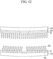
- the liquid crystal display may differentiate the pre-tilt angle of the liquid crystal molecules 310 adjacent to the first alignment layer 11 and the pre-tilt angle of the liquid crystal molecules 310 adjacent to the second alignment layer 21. Accordingly, as shown in FIG. 12 , although the display panel is bent to form the curved liquid crystal display, the texture region may not be generated in the boundary of the adjacent domain regions.
- FIG. 7 to FIG. 11 are views showing a manufacturing method of a liquid crystal display according to an embodiment.
- the configurations included in the lower panel 100 and the upper panel 200 shown in FIG. 4 may be respectively manufactured in the first substrate 110 and the second substrate 210.
- the gate electrode 124, the source electrode 173, the drain electrode 175, and the pixel electrode 191 are formed on the first substrate 110, and the common electrode 270 is formed on the second substrate 210.
- the first alignment layer 11 may be formed to cover the pixel electrode positioned on the first substrate 110, and although not shown in FIG. 7 , the second alignment layer may be formed to cover the common electrode on the second substrate like the first alignment layer 11.
- the first polymer included in the alignment material includes the first main chain and the plurality of first side chains connected to the first main chain, and at least one among the plurality of first side chains includes the photoreactive group.
- the photoreactive group and the reactive mesogen 12 may use the above-described material.
- the reactive mesogen 12 may be added in the range of, for example, 7 wt% to 25 wt% for a solid of the alignment material.
- the reactive mesogen 12 may be added in the range of 10 wt% to 20 wt%, 12 wt% to 18 wt% or 14 wt% to 16 wt%.
- the content of about 15 wt% may be added.
- a mixture of the alignment material including the second polymer (which may be, for example, a polyimide) and the reactive mesogen 12 is coated on the second substrate 210 and the bake process is performed to form the second alignment layer.
- the second polymer which may be, for example, a polyimide
- Phase separation may be generated during the above-described bake process, and as described FIG. 3 , the upper and lower alignment layers and the buffer region positioned therebetween may be formed.
- the polymerization of the reactive mesogen 12 may be initialized by the heat generated in the bake process, however, when using the above-described reactive mesogen 12 according to an embodiment, the reactive mesogen 12 has heat resistance such that the reactive mesogen 12 may be prevented from being previously polymerized in the bake process. Accordingly, the reactivity of the reactive mesogen 12 by the ultraviolet rays irradiation may be maintained.
- the reactive mesogen 12 is mixed in both the first alignment layer 11 and the second alignment layer 21; however, the reactive mesogen 12 may only be mixed in one of the first alignment layer 11 and the second alignment layer 21.
- the liquid crystal material 31 including the liquid crystal molecules is dripped on the first alignment layer 11, and referring to FIG. 9 , the lower panel 100 and the upper panel 200 manufactured as above-described are assembled.
- the heat treatment may be performed to uniformly spread the liquid crystal material 31 dripped in FIG. 8 , and in this case, the reactive mesogen 12 included in the alignment layers 11 and 21 is adsorbed into the liquid crystal layer 3.
- the light is irradiated.
- the light may be ultraviolet light having a wavelength that is appropriate for polymerizing the reactive mesogen 12.
- the reactive mesogen 12 moves into the surface of the alignment layers 11 and 21 such that the plurality of protrusions 15 are formed.
- the only first alignment layer 11 includes the photoreactive group such that the polymerization reaction speed causes the difference in the portions adjacent to the first alignment layer 11 and the second alignment layer 21. That is, the reactive mesogen 12 polymerized by the photoreactive group of the first alignment layer 11 mainly forms the plurality of protrusions 15 in the surface of the first alignment layer 11.
- the photoreactive group is also chemically combined with the reactive mesogen, thereby forming the polymer forming the plurality of protrusions 15.
- FIG. 12 is a view showing a display panel that is bent to form a curved liquid crystal display in a liquid crystal display according to an embodiment of FIG. 6 .
- FIG. 12 only schematically shows the first and second substrates 110 and 210 facing each other, the pixel electrode 191, the common electrode 270, the first and second alignment layers 11 and 21, and the liquid crystal molecules 310.
- the first substrate 110 and the second substrate 210 may be bent to have the curved surface.
- the region where the pre-tilt direction of the liquid crystal molecules adjacent to the first alignment layer and the pre-tilt direction of the liquid crystal molecules adjacent to the second alignment layer are different may be generated. This region may be generated in the boundary portion of the adjacent domains. In this region, the direction that the liquid crystal molecules are inclined may be misaligned such that the texture defect is undesirably generated in the screen.
- the texture region is not generated on the boundary of the adjacent domain regions.
- a vertical alignment mode liquid crystal display which arranges major axes of liquid crystal molecules so as to be perpendicular to the display panel when an electric field is not applied, has been widely used due to its high contrast ratio and wide reference viewing angle.
- a curved liquid crystal display may be realized by bending a flat liquid crystal display through a bending process. However, if a misalignment is generated between the upper and lower display panels overlapping each other, the transmittance may be lowered.
- Embodiments may provide a liquid crystal display and a manufacturing method thereof for preventing an afterimage and a stain from being generated.
- a reactive mesogen having strong heat resistance and excellent reactivity may be used, and an afterimage and a stain may be prevented from being generated in the liquid crystal display.
Landscapes
- Physics & Mathematics (AREA)
- Chemical & Material Sciences (AREA)
- Nonlinear Science (AREA)
- Crystallography & Structural Chemistry (AREA)
- Optics & Photonics (AREA)
- General Physics & Mathematics (AREA)
- Mathematical Physics (AREA)
- Spectroscopy & Molecular Physics (AREA)
- Engineering & Computer Science (AREA)
- Organic Chemistry (AREA)
- Materials Engineering (AREA)
- Geometry (AREA)
- Microelectronics & Electronic Packaging (AREA)
- Polymers & Plastics (AREA)
- Medicinal Chemistry (AREA)
- Chemical Kinetics & Catalysis (AREA)
- Health & Medical Sciences (AREA)
- Liquid Crystal (AREA)
Abstract

Description
- The present invention relates to a liquid crystal display and a manufacturing method thereof.
- A liquid crystal display includes a display panel including field generating electrodes such as a pixel electrode and a common electrode, and a liquid crystal layer formed in an electric field generated by the field generating electrodes. The liquid crystal display forms the electric field to the liquid crystal layer, thereby displaying an image by determining an arrangement of liquid crystal molecules included in the liquid crystal layer and controlling transmittance of a light passing through the liquid crystal layer.
- The above information disclosed in this Background section is only for enhancement of understanding of the background of the invention and therefore it may contain information that does not form the prior art that is already known in this country to a person of ordinary skill in the art.
- One aspect of the present invention is directed to a liquid crystal display, including a first substrate; a second substrate overlapping the first substrate; a liquid crystal layer positioned between the first substrate and the second substrate and including a plurality of liquid crystal molecules; a first alignment layer positioned between the first substrate and the liquid crystal layer; a second alignment layer positioned between the second substrate and the liquid crystal layer; and a plurality of protrusions positioned at at least one of between the first alignment layer and the liquid crystal layer and between the second alignment layer and the liquid crystal layer, wherein at least one among the plurality of protrusions includes a polymer of a reactive mesogen, and the reactive mesogen is represented by Chemical Formula 1.

- In Chemical Formula 1, Pa and Pb are independently an acrylate group or a methacrylate group,
A1 includes
A2 includes any one of

- n
- is a natural number of 2 to 5.
- The first alignment layer may include a first polymer, the first polymer may include a first main chain and a plurality of first side chains connected to the first main chain, and at least one among the plurality of first side chains may include at least one of a photoreactive group and a photoreactive group derivative.
- The photoreactive group derivative included in the plurality of first side chains may be combined with the polymer of the reactive mesogen included in the plurality of protrusions.
- The second alignment layer may include a second polymer, the second polymer includes a second main chain and a plurality of second side chains connected to the second main chain, and the plurality of second side chains do not include the photo reactive group and the photoreactive group derivative.
- The reactive mesogen may be represented by Chemical Formula A or Chemical Formula B.


- In Chemical Formula A and Chemical Formula B, Pa and Pb are independently the acrylate group or the methacrylate group, S is one selected from a group including F, Cl, and Br, x is 0, 1, 2, or 3, and n is the natural number of 2 to 5.
- The reactive mesogen may have heat resistance of 250 degrees Celsius or more.
- The density of the protrusions positioned between the first alignment layer and the liquid crystal layer may be higher than the density of the protrusions positioned between the second alignment layer and the liquid crystal layer among the plurality of protrusions.
- The pre-tilt angle of the liquid crystal molecules adjacent to the first alignment layer among the plurality of liquid crystal molecules may be larger than the pre-tilt angle of the liquid crystal molecules adjacent to the second alignment layer among the plurality of liquid crystal molecules.
- The first substrate and the second substrate may have a curved surface.
- The liquid crystal display may further include: a thin film transistor positioned between the first substrate and the first alignment layer; a pixel electrode connected to the thin film transistor; and a common electrode forming an electric field with the pixel electrode.
- The first alignment layer may include a lower alignment layer, an upper alignment layer, and a buffer region positioned between the lower alignment layer and the upper alignment layer, the upper alignment layer may include at least one of the photoreactive group and the photoreactive group derivative, the lower alignment layer may not include the photoreactive group and the photoreactive group derivative, and the buffer region may include less of the photoreactive group than the content of at least one of the photoreactive group and the photoreactive group derivative of the upper alignment layer.
- The size of the protrusions positioned between the first alignment layer and the liquid crystal layer may be smaller than the size of the protrusions positioned between the second alignment layer and the liquid crystal layer.
- Another aspect of the present invention is directed to a manufacturing method of a liquid crystal display, including preparing a lower panel including a first alignment layer positioned on a first substrate; preparing an upper panel including a second alignment layer positioned on a second substrate; forming a liquid crystal layer positioned between the lower panel and the upper panel and including a plurality of liquid crystal molecules; heat-treating the upper panel and the lower panel; and irradiating light to the lower panel, the upper panel, and the liquid crystal layer in a state in which an electric field is applied to the liquid crystal layer, and in the step of the heat treatment, a reactive mesogen included in at least one of the first alignment layer and the second alignment layer is adsorbed into the liquid crystal layer, in the light irradiation step, the reactive mesogen is polymerized to form a plurality of protrusions, and the reactive mesogen is represented by Chemical Formula 1.

- In Chemical Formula 1, Pa and Pb are independently an acrylate group or a methacrylate group,
A1 includes
A2 includes any one of

n is a natural number of 2 to 5. - The first alignment layer may include a first polymer, the first polymer may include a first main chain and a plurality of first side chains connected to the first main chain, and at least one among the plurality of first side chains may include a photoreactive group.
- The second alignment layer may include a second polymer, the second polymer may include a second main chain and a plurality of second side chains connected to the second main chain, and the plurality of second side chains may not include the photoreactive group.
- The reactive mesogen may be represented by Chemical Formula A or Chemical Formula B.


- In Chemical Formula A and Chemical Formula B, Pa and Pb are independently the acrylate group or the methacrylate group, S is one selected from a group including F, Cl, and Br, x is 0, 1, 2, or 3, and n is the natural number of 2 to 5.
- The density of the plurality of protrusions positioned between the first alignment layer and the liquid crystal layer may be larger than the density of the plurality of protrusions positioned between the second alignment layer and the liquid crystal layer.
- Among the plurality of protrusions, the density of the protrusions positioned between the first alignment layer and the liquid crystal layer may be higher than the density of the protrusions positioned between the second alignment layer and the liquid crystal layer.
- After the step of light irradiation, the pre-tilt angle of the liquid crystal molecules adjacent to the first alignment layer among the plurality of liquid crystal molecules may be larger than the pre-tilt angle of the liquid crystal molecules adjacent to the second alignment layer among the plurality of liquid crystal molecules.
- The manufacturing method of the liquid crystal display may further include providing a curved surface to the first substrate and the second substrate.
- The first alignment layer may be divided into a lower alignment layer and an upper alignment layer, a buffer region is formed between the lower alignment layer and the upper alignment layer, the upper alignment layer may include the photoreactive group, the lower alignment layer may not include the photoreactive group, and the buffer region may include less of the photoreactive group than the content of the photoreactive group distributed in the upper alignment layer.
- The manufacturing method may be used to manufacture a liquid crystal display described herein.
- Another aspect of the present invention is directed to a liquid crystal display, including a first substrate, a second substrate facing the first substrate, a liquid crystal layer between the first substrate and the second substrate, and an alignment layer between the first substrate and the second substrate and adjacent to the liquid crystal layer, the alignment layer having protruding polymeric structures, the polymeric structures being coupled to the material of the alignment layer via a (meth)acrylate moiety, the polymeric structures including a polymer unit having a first moiety that is a divalent biphenyl moiety, a diether linkage in which two oxygens are joined by a carbon chain of 2 to 5 carbons, and a second moiety that is a divalent phenyl or biphenyl moiety, wherein the first and second moieties are connected by the diether linkage.
- The polymer unit may be represented by Chemical Formula 2:

- A1 may include


- In A1, at least one hydrogen connected to a carbon ring may be substituted with F, Cl, or Br.
- In A2, at least one hydrogen connected to a carbon ring may be substituted with F, Cl, or Br.
- At least some of the above and other features of the invention are set out in the claims.
- Features will become apparent to those of skill in the art by describing in detail embodiments with reference to the attached drawings in which:
-
FIG. 1 illustrates a cross-sectional view showing a liquid crystal display according to an embodiment. -
FIG. 2 illustrates a schematic top plan view showing a pixel electrode structure ofFIG. 1 . -
FIG. 3 illustrates a schematic cross-sectional view showing an alignment layer structure ofFIG. 1 . -
FIG. 4 illustrates a cross-sectional view of a liquid crystal display according to a variation embodiment ofFIG. 1 . -
FIG. 5 illustrates a view explaining a texture defect by a misalignment when pre-tilt angles of liquid crystal molecules adjacent to upper and lower alignment layers are the same. -
FIG. 6 illustrates a view schematically showing an arrangement of liquid crystal molecules adjacent to upper and lower alignment layers in a liquid crystal display according to an embodiment described inFIG. 4 . -
FIG. 7 to FIG. 11 illustrate views showing a manufacturing method of a liquid crystal display according to an embodiment. -
FIG. 12 illustrates a view showing a display panel that is bent to form a curved liquid crystal display in a liquid crystal display according to an embodiment ofFIG. 6 . - Embodiments will now be described more fully hereinafter with reference to the accompanying drawings; however, they may be embodied in different forms and should not be construed as limited to the embodiments set forth herein. Rather, these embodiments are provided so that this disclosure will be thorough and complete, and will fully convey example implementations to those skilled in the art.
- In the drawing figures, the dimensions of layers and regions may be exaggerated for clarity of illustration. Like reference numerals refer to like elements throughout.
- It will be understood that when an element such as a layer, film, region, or substrate is referred to as being "on" another element, it can be directly on the other element, or intervening elements may also be present. In contrast, when an element is referred to as being "directly on" another element, there are no intervening elements present. Further, in the specification, the word "on" means positioning on or below the object portion, but does not essentially mean positioning on the upper side of the object portion based on a gravity direction.
- Further, in the specification, the phrase "on a flat surface" means when an object portion is viewed from above, and the phrase "on a cross-section" means when a cross-section taken by vertically cutting an object portion is viewed from the side.
-
FIG. 1 is a cross-sectional view showing a liquid crystal display according to an embodiment.FIG. 2 is a schematic top plan view showing a pixel electrode structure ofFIG. 1 . - Referring to
FIG. 1 , the liquid crystal display according to the present embodiment includes alower panel 100 and anupper panel 200 overlapping each other, and aliquid crystal layer 3 interposed between the twodisplay panels - The
lower panel 100 includes afirst alignment layer 11 positioned at one side facing theliquid crystal layer 3, and theupper panel 200 includes asecond alignment layer 21 positioned at one side facing theliquid crystal layer 3. - In the present embodiment, a plurality of
protrusions first alignment layer 11 and theliquid crystal layer 3 and between thesecond alignment layer 21 and theliquid crystal layer 3. - At least one of the plurality of
protrusions 
- In Chemical Formula 1, Pa and Pb are (meth)acrylate terminal moieties, and are each independently an acrylate group or a methacrylate group. A1 includes a divalent biphenyl moiety


- Herein, the term "carbon ring" indicates carbons connected to each other to form a ring.
- In Chemical Formula 1, when a component to be polymerized like the acrylate group or the methacrylate group receives ultraviolet rays, a crosslinking reaction is generated such that the polymer may be formed. The reactive mesogen may be polymerized within itself such that the plurality of
protrusions - Additional aspects of the reactive mesogen will now be described in detail.
- In the present embodiment, the reactive mesogen may have a three or four ring structure. For example, in Chemical Formula 1, A1 has two ring structures, A2 may have one or two ring structures. Ring structures adjacent to each other are connected by a spacer such as -O-(CH2)n O-. By having at least three ring structures, heat resistance may be improved. In the present embodiment, the reactive mesogen has heat resistance to more than about 250 degrees Celsius such that the reactivity may be small at less than the temperature.
- When the ring structure has three or more, a length of a part that becomes a conjugation is elongated, and an ultraviolet ray absorption wavelength band may move into a long wavelength such that the reactivity for the ultraviolet rays may increase. If the reactivity substantially increases, most of the reactive mesogen may be polymerized and moves into the
first alignment layer 11 or thesecond alignment layer 21 to decrease surface energy, thereby forming the protrusion. In this case, directivity in which the polymerized reactive mesogen moves to either alignment layer side of thefirst alignment layer 11 and thesecond alignment layer 21 may not be uniform. Accordingly, selectivity ofliquid crystal molecules 310 respectively adjacent to the upper andlower panels - According to the present embodiment, the reactive mesogen may have a spacer within the three or four ring structure, which may improve selectivity. Accordingly, the three or more ring structure may not be directly connected, and the length of the part that forms the conjugation may be reduced.
- According to the present embodiment, the spacer includes an ether group (-O-) having stability (instead of, for example, an ester group (-COO-) included in the reactive mesogen represented by Chemical Formula X and Chemical Formula Y, below) such that the spacer portion may be prevented from being disconnected when irradiated with ultraviolet rays.


- According to the present embodiment, the spacer includes an alkylene group in which a carbon number is 2 to 5.
- In general, if the length of the spacer is elongated, the solubility may increase. At the same time, a deformation may be more easily generated by an external stress, and the
liquid crystal molecule 310 may not fully return to an initial position in a voltage off state. In such a case, an afterimage may be significant. If the length of the spacer is short, the solubility may be reduced. At this same time, rigidity may be increased, and afterimage may be reduced. The solubility means a degree that the reactive mesogen may be dissolved in the solvent of the alignment material. In the present embodiment, the carbon number of the alkylene group included in the spacer has the range of 2 to 5. In the present embodiment, an afterimage level that does not significantly affect the quality of the product may be maintained and the reactive mesogen may have solubility of a degree that it may be coated along with the alignment material by being dissolved in the solvent. - According to the present embodiment, the ring structure has a -C6H4C6H4- of a biphenylene structure, and the molecule structure may have a plane shape. In this structure, an attraction force may be more easily generated between the molecules such that it tends to be easily crystallized. Accordingly, the solubility may be low.
- In an embodiment, at least one hydrogen connected to the carbon ring may be substituted, for example, with F. Thus, a degree of crystallinity may be reduced by increasing a free volume. Here, the free volume may mean an empty space around a configuration particle among a volume occupied with a material.
- As a substituent, for example, F, Cl, or Br may be used. Cl and Br have a larger atom size than F. Cl and Br may be more easily separated from the reactive mesogen to be easily made into an ionic material. In an embodiment, F is the substituent.
- According to the present embodiment, the reactive mesogen may be represented by Chemical Formula A or Chemical Formula B.


- In Chemical Formula A and Chemical Formula B, Pa and Pb are independently an acrylate group or a methacrylate group, S is one selected from a group including F, Cl, and Br, x is 0, 1, 2, or 3, and n is a natural number of 2 to 5.
- In the reactive mesogen represented by Chemical Formula A, two ring structures and one ring structure are connected by the spacer, while in the reactive mesogen represented by Chemical Formula B, two ring structures and two ring structures are connected by the spacer.
- The reactive mesogen represented by Chemical Formula B includes four ring structures. In Chemical Formula B, x may be 1 or more and/or n may be 2 or more.
- According to the present embodiment, the reactive mesogen may include, for example, at least one among a group represented by Chemical Formula A-1 to Chemical Formula A-10. A reactive mesogen satisfying the structure of the above-described Chemical Formula A or Chemical Formula B may be included as well as those below.


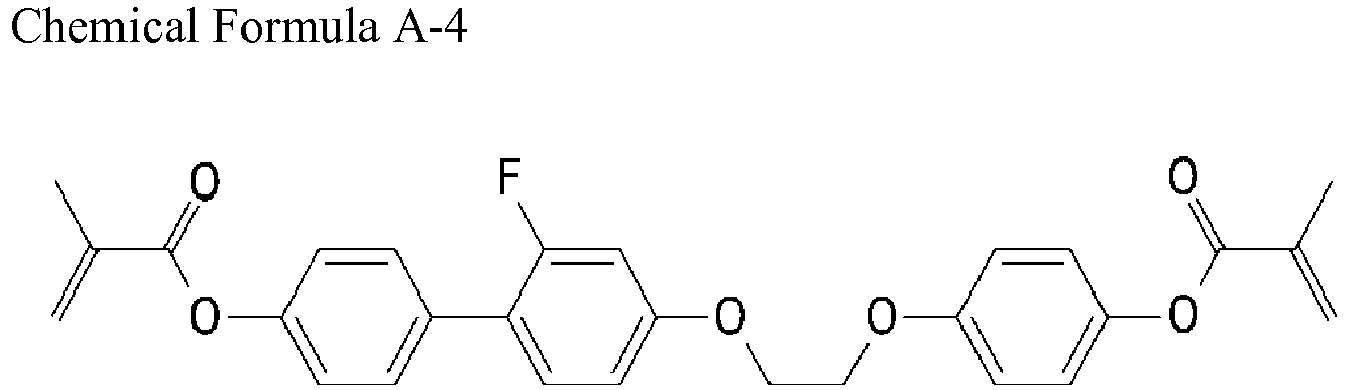


- Below, other constituent elements of the
lower panel 100 will be described. - Again referring to
FIG. 1 , a plurality of gate lines are positioned on afirst substrate 110. Each gate line includes agate electrode 124 that is protruded from the gate line or a part of the gate line. Agate insulating layer 140 is positioned on thegate electrode 124, asemiconductor layer 154 is positioned on thegate insulating layer 140, and thesemiconductor layer 154 overlaps thegate electrode 124. - The
semiconductor layer 154 may include amorphous silicon, polycrystalline silicon, or an oxide semiconductor. -
Ohmic contacts semiconductor layer 154. Theohmic contacts ohmic contacts - A
source electrode 173 and adrain electrode 175 are positioned on theohmic contacts gate insulating layer 140. A plurality of data lines may be positioned on thegate insulating layer 140, and each data line may be connected to asource electrode 173. - The
gate electrode 124, thesource electrode 173, and thedrain electrode 175 form a thin film transistor as a switching element along with thesemiconductor layer 154. - A first insulating
layer 180a is positioned on thesource electrode 173 and thedrain electrode 175, and the first insulatinglayer 180a may be in contact with thesemiconductor layer 154 in a separate space between thesource electrode 173 and thedrain electrode 175. The first insulatinglayer 180a may be made of the organic insulating material or the inorganic insulating material, and may include a single layer or a multilayer. - A
color filter 230 may be positioned on the first insulatinglayer 180a. Thecolor filter 230 may display one of primary colors such as three primary colors of red, green, and blue, or the like. In an implementation, thecolor filter 230 may represent colors such as cyan, magenta, yellow, and a white-containing color. - A second insulating
layer 180b may be positioned on thecolor filter 230, and the second insulatinglayer 180b may include the inorganic insulating material or the organic insulating material. The secondinsulating layer 180b, as an overcoat for thecolor filter 230, may be used to help prevent the color filter from being exposed outside and for realizing a flat surface. The secondinsulating layer 180b may be omitted. - A
pixel electrode 191 is positioned on the second insulatinglayer 180b, and thepixel electrode 191 is mainly positioned in a transmission region TA. The above-described gate line, data line, thin film transistor, and the like may be positioned in a light blocking region BA where light is not transmitted. The transmission region TA as a region where the image is mainly displayed is a region where the light may be transmitted, and the light blocking region BA is not a region for displaying the image and may be a region where the light may not be mainly transmitted. - The first insulating
layer 180a and the second insulatinglayer 180b have acontact hole 185, and thedrain electrode 175 and thepixel electrode 191 are electrically connected to each other through thecontact hole 185. - Referring to
FIG. 2 , thepixel electrode 191 includes a cross-shaped stem portion including alongitudinal stem portion 192 and atransverse stem portion 193 crossing thelongitudinal stem portion 192. Also, thepixel electrode 191 is divided into a first sub-region Da, a second sub-region Db, a third sub-region Dc, and a fourth sub-region Dd by thelongitudinal stem portion 192 and thetransverse stem portion 193, and each sub-region includes a plurality of first to fourth fine branchedportions - The first fine branched
portion 194a extends obliquely in an upper left direction from thetransverse stem portion 193 or thelongitudinal stem portion 192, and the second fine branchedportion 194b extends obliquely in an upper right direction from thetransverse stem portion 193 or thelongitudinal stem portion 192. In addition, the third fine branchedportion 194c extends obliquely in a lower left direction from thetransverse stem portion 193 or thelongitudinal stem portion 192, and the fourth fine branchedportion 194d extends obliquely in a lower right direction from thetransverse stem portion 193 or thelongitudinal stem portion 192. - If voltages are applied to the
pixel electrode 191 shown inFIG. 1 and acommon electrode 270 that will be described below, theliquid crystal molecules 310 are inclined such that a long axis thereof is aligned in a direction perpendicular to a direction of an electric field by the electric field formed to theliquid crystal layer 3. The change degree of polarization of the light that is incident to theliquid crystal layer 3 is changed according to the inclination degree of theliquid crystal molecules 310, and this change of polarization appears as a change of transmittance by the polarizer, thereby displaying images of the liquid crystal display. - A direction in which the
liquid crystal molecule 310 is inclined is determined by the fine branchedportions pixel electrode 191, and theliquid crystal molecule 310 is inclined toward a direction parallel with length directions of the fine branchedportions pixel electrode 191 includes four subregions Da, Db, Dc, and Dd in which the length directions of the fine branchedportions liquid crystal molecules 310 are inclined is approximately four directions. In this case, theliquid crystal layer 3 is formed with four domains in which the alignment directions of theliquid crystal molecules 310 are different. As described above, the direction in which the liquid crystal molecules are inclined varies, such that the viewing angle of the liquid crystal display may be improved. - Again referring to
FIG. 1 , alight blocking member 220 is positioned on the second insulatinglayer 180b and thepixel electrode 191. Thelight blocking member 220 is positioned in the light blocking region BA. Thelight blocking member 220 is referred to as a black matrix. - The
light blocking member 220 includes aspacer 221 and a mainlight blocking portion 222. The mainlight blocking portion 222 to prevent light leakage is formed in the light blocking region BA positioned with the gate line, the data line, the thin film transistor, and the like, and the mainlight blocking portion 222 may have a substantially flat upper surface. The mainlight blocking portion 222 may overlap thecontact hole 185. The mainlight blocking portion 222 overlapping thecontact hole 185 fills the step generated in thecontact hole 185, thereby flattening the surface and preventing light leakage therearound. - The
spacer 221 is connected to the mainlight blocking portion 222. Thespacer 221 may be positioned on the signal line such as gate line and the data line, and/or the thin film transistor. InFIG. 1 , thespacer 221 is separated from theupper panel 200, as an example variation, thespacer 221 and theupper panel 200 may be in contact. - The
spacer 221 serves to maintain a cell gap between theupper panel 200 and thelower panel 100. For example, when a distance between theupper panel 200 and thelower panel 100 becomes narrow by an external pressure against the liquid crystal display, it has a function of maintaining the cell gap between theupper panel 200 and thelower panel 100. - Here, the described content simultaneously forming the main
light blocking portion 222 and thespacer 221 may be varied, and as an example variation, the mainlight blocking portion 222 and thespacer 221 may be separately formed. - The
first alignment layer 11 is positioned on thepixel electrode 191. In the present embodiment, thefirst alignment layer 11 includes a first polymer, the first polymer includes a first main chain and a plurality of first side chains connected to the first main chain, and at least one among a plurality of first side chains may include one among a photoreactive group and a photoreactive group derivative. Here, the photo reactive group derivative means a structure in which the photoreactive group irradiated with ultraviolet rays is chemically combined with the reactive mesogen to be modified. At least one among the plurality of first side chains may include a vertical alignment group. - The photoreactive group may use various materials that may generate a radical by absorbing the light to initiate a polymerization reaction.
- According to the present embodiment, the photoreactive group may include at least one among a group represented by Chemical Formula 1a to Chemical Formula 12a.


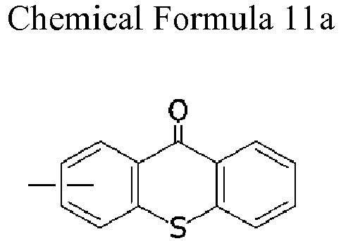
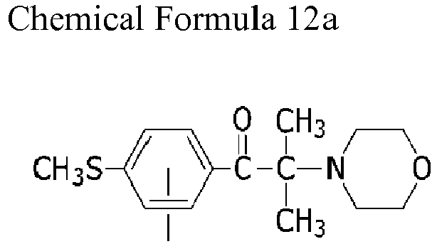
- Alternatively, the
first alignment layer 11 may not include the photoreactive group or the photoreactive group derivative, and in this case, the plurality ofprotrusions 15 may also be formed in the surface of thefirst alignment layer 11 by the polymerization reaction of the reactive mesogen by ultraviolet rays. - Referring to the
upper panel 200, thecommon electrode 270 may be positioned between asecond substrate 210 and theliquid crystal layer 3. Thecommon electrode 270 may be formed as a whole plate on the entire surface of thesecond substrate 210 facing theliquid crystal layer 3. Thesecond alignment layer 21 is positioned between thecommon electrode 270 and theliquid crystal layer 3, and thesecond alignment layer 21 may be an alignment layer made of the same components as the above-describedfirst alignment layer 11. - The
liquid crystal layer 3 includes theliquid crystal molecules 310. Theliquid crystal molecule 310 may have negative dielectric anisotropy such that theliquid crystal molecules 310 may be aligned in the direction substantially perpendicular to the first andsecond substrates liquid crystal layer 3. Theliquid crystal molecules 310 may have the pre-tilt in the predetermined direction by the plurality of above-describedprotrusions liquid crystal layer 3. - In the present embodiment, the liquid crystal layer may not include a photoinitiator. A photoinitiator included in the liquid crystal layer may remain after irradiation of the ultraviolet rays and may function as an impurity, which may cause a surface afterimage.
-
FIG. 3 is a schematic cross-sectional view showing an alignment layer structure ofFIG. 1 . InFIG. 3 , for convenience of the description, other constituent elements are omitted, and only thefirst alignment layer 11 positioned on thefirst substrate 110 shown inFIG. 1 is schematically shown. - Referring to
FIG. 3 , thefirst alignment layer 11 includes alower alignment layer 11a, anupper alignment layer 11c, and abuffer region 11b positioned between thelower alignment layer 11a and theupper alignment layer 11c. Thelower alignment layer 11a mainly includes the vertical alignment group of which the side chain is connected to the main chain and a component to improve a voltage holding rate, and theupper alignment layer 11c mainly includes the side chain including at least one of the photoreactive group and the photoreactive group derivative. - A bake process may be performed in the process of forming the alignment layer, and in this case, the alignment layer may be phase-divided into the
lower alignment layer 11a and theupper alignment layer 11c by a surface energy difference.Buffer region 11b may be formed between phases. Thebuffer region 11b is a part where the component of thelower alignment layer 11 a and the component of theupper alignment layer 11c are mixed, and thebuffer region 11b may include a smaller amount of the photoreactive group than the content of at least one of the photoreactive group and the photoreactive group derivative included in theupper alignment layer 11c. To improve the afterimage, the component of theupper alignment layer 11c may be about 30 wt% or more of the entire component of thefirst alignment layer 11. -
FIG. 4 is a cross-sectional view of a liquid crystal display according to a variation embodiment ofFIG. 1 . -
FIG. 4 is the cross-sectional view of the liquid crystal display according to an embodiment, and it is the description related to the embodiment that reduces the texture of the curved liquid crystal display. - Referring to
FIG. 4 , most constituent elements are the same as those described inFIG. 1 , and differences will be described. - Referring to
FIG. 4 , thefirst alignment layer 11 is positioned between thepixel electrode 191 and theliquid crystal layer 3, and thesecond alignment layer 21 is positioned between thecommon electrode 270 and theliquid crystal layer 3. - The first and second alignment layers 11 and 21 may be vertical alignment layers. The
first alignment layer 11 includes the first polymer, the first polymer includes the first main chain and the plurality of first side chains connected to the first main chain, and at least one among the plurality of first side chains may include at least one of the photoreactive group and the photoreactive group derivative. - The
second alignment layer 21 includes the second polymer, the second polymer includes the second main chain and the plurality of second side chains connected to the second main chain, and the plurality of second side chains may not include the photoreactive group and the photoreactive group derivative. - The photoreactive group included in the side chain may help increase the reaction speed during the polymerization of the reactive mesogen by the irradiation of ultraviolet rays. Accordingly, the plurality of
protrusions 15 may be mainly formed in the surface of thefirst alignment layer 11. - The reactive mesogen mixed in the alignment material forming the first and second alignment layers 11 and 21 may be eluted into the
liquid crystal layer 3 in the heat treatment process, and may be photoirradiated such that the polymer included in theprotrusion 15 may be formed. - The plurality of
protrusions 15 may help control the pre-tilt as the initial alignment direction of theliquid crystal molecules 310. The photoreactive group included in the side chain of the polymer of thefirst alignment layer 11 may help improve the polymerization reaction speed of the reactive mesogen. Accordingly, the pre-tilt angles of theliquid crystal molecules 310 adjacent to thesecond alignment layer 21 and theliquid crystal molecules 310 adjacent to thefirst alignment layer 11 may be different. - Herein, "pre-tilt" means that the
liquid crystal molecule 310 is inclined with reference to the direction perpendicular to the surface of thefirst alignment layer 11 or thesecond alignment layer 21, and "pre-tilt angle" means the inclined degree, that is, the inclined angle with reference to an axis perpendicular to thefirst alignment layer 11 or thesecond alignment layer 21. - As shown in
FIG. 4 , the plurality ofprotrusions 15 may only be between thefirst alignment layer 11 and theliquid crystal layer 3, or as an example variation, the plurality of protrusions may be formed between thesecond alignment layer 21 and theliquid crystal layer 3, and in this case, the number of the plurality of protrusions formed between thesecond alignment layer 21 and theliquid crystal layer 3 may be significantly smaller than the number of the plurality ofprotrusions 15 formed between thefirst alignment layer 11 and theliquid crystal layer 3. For example, comparing a protrusion density (corresponding to the number of protrusions in a unit area), the density of the plurality of protrusions positioned between thefirst alignment layer 11 and theliquid crystal layer 3 is larger than the density of the plurality of protrusions positioned between thesecond alignment layer 21 and theliquid crystal layer 3. In this case, the size of the protrusions positioned between thefirst alignment layer 11 and theliquid crystal layer 3 is smaller than the size of the protrusions positioned between thesecond alignment layer 21 and theliquid crystal layer 3. - By differentiating the protrusion density of the
lower panel 100 and theupper panel 200, the pre-tilt angle of theliquid crystal molecules 310 adjacent to thefirst alignment layer 11 and the pre-tilt angle of theliquid crystal molecules 310 adjacent to thesecond alignment layer 21 may be differentiated. As the density of theprotrusions 15 positioned on thefirst alignment layer 11 increases, the pre-tilt angle of theliquid crystal molecules 310 adjacent to thefirst alignment layer 11 may be larger than the pre-tilt angle of theliquid crystal molecules 310 adjacent to thesecond alignment layer 21. - For example, the
liquid crystal molecules 310 adjacent to thefirst alignment layer 11 may have an angle of more than 80 degrees to less than 89 degrees with respect to the surface of thefirst alignment layer 11. Theliquid crystal molecules 310 adjacent to thesecond alignment layer 21 may be arranged at an angle of more than 89 degrees to 90 degrees or less, to be close to substantially perpendicular to the surface of thesecond alignment layer 21. -
FIG. 5 is a view explaining a texture defect by a misalignment when pre-tilt angles of liquid crystal molecules adjacent to upper and lower alignment layers are the same. -
FIG. 5 , for convenience of explanation, schematically shows the first andsecond substrates liquid crystal molecules 310. Also,FIG. 5 shows the part corresponding to the transmission region TA in the region shown inFIG. 4 and the cross-section taken along the horizontal direction of the display panel. The horizontal direction corresponds to a right/left direction when viewers view the liquid crystal display. - Between the
first alignment layer 11 and thesecond alignment layer 21, in the region where thefirst alignment layer 11 and thesecond alignment layer 21 overlap each other, when theliquid crystal molecules 310 form the pre-tilt in the same direction, if the display panel is misaligned, the region where the direction of the pre-tilt of theliquid crystal molecules 310 adjacent to thefirst alignment layer 11 and the direction of the pre-tilt of theliquid crystal molecules 310 adjacent to thesecond alignment layer 21 are misaligned may be generated. This region may be generated in the boundary portion of the adjacent domains, and the direction that theliquid crystal molecules 310 are inclined may be misaligned such that a texture defect is generated in the screen. The misalignment of the display panel may be generated when bending the display panel. The texture corresponds to a dark part that appears darker than the surroundings and may be recognized as a stain. -
FIG. 6 is a view schematically showing an arrangement of liquid crystal molecules adjacent to upper and lower alignment layers in a liquid crystal display according to an embodiment described inFIG. 4 . - For convenience of description,
FIG. 6 schematically shows the first andsecond substrates FIG. 4 , thepixel electrode 191, thecommon electrode 270, the first and second alignment layers 11 and 21, and theliquid crystal molecules 310. Also, among the region shown inFIG. 4 ,FIG. 6 shows the portion corresponding to the transmission region TA and is taken along the horizontal direction of the display panel. The horizontal direction corresponds to a right/left direction when viewers view the liquid crystal display. - Referring to
FIG. 6 , the liquid crystal display according to an embodiment may differentiate the pre-tilt angle of theliquid crystal molecules 310 adjacent to thefirst alignment layer 11 and the pre-tilt angle of theliquid crystal molecules 310 adjacent to thesecond alignment layer 21. Accordingly, as shown inFIG. 12 , although the display panel is bent to form the curved liquid crystal display, the texture region may not be generated in the boundary of the adjacent domain regions. -
FIG. 7 to FIG. 11 are views showing a manufacturing method of a liquid crystal display according to an embodiment. - Firstly, the configurations included in the
lower panel 100 and theupper panel 200 shown inFIG. 4 may be respectively manufactured in thefirst substrate 110 and thesecond substrate 210. - For example, in
FIG. 4 , thegate electrode 124, thesource electrode 173, thedrain electrode 175, and thepixel electrode 191 are formed on thefirst substrate 110, and thecommon electrode 270 is formed on thesecond substrate 210. - Referring to
FIG. 7 , thefirst alignment layer 11 may be formed to cover the pixel electrode positioned on thefirst substrate 110, and although not shown inFIG. 7 , the second alignment layer may be formed to cover the common electrode on the second substrate like thefirst alignment layer 11. - In detail, a mixture of the alignment material including the first polymer (which may be, for example, a polyimide) and the
reactive mesogen 12 is coated on thefirst substrate 110, and a bake process is performed to form thefirst alignment layer 11. According to the present embodiment, the first polymer included in the alignment material includes the first main chain and the plurality of first side chains connected to the first main chain, and at least one among the plurality of first side chains includes the photoreactive group. The photoreactive group and thereactive mesogen 12 may use the above-described material. Thereactive mesogen 12 may be added in the range of, for example, 7 wt% to 25 wt% for a solid of the alignment material. For example, thereactive mesogen 12 may be added in the range of 10 wt% to 20 wt%, 12 wt% to 18 wt% or 14 wt% to 16 wt%. For example, the content of about 15 wt% may be added. - A mixture of the alignment material including the second polymer (which may be, for example, a polyimide) and the
reactive mesogen 12 is coated on thesecond substrate 210 and the bake process is performed to form the second alignment layer. - Phase separation may be generated during the above-described bake process, and as described
FIG. 3 , the upper and lower alignment layers and the buffer region positioned therebetween may be formed. - The polymerization of the
reactive mesogen 12 may be initialized by the heat generated in the bake process, however, when using the above-describedreactive mesogen 12 according to an embodiment, thereactive mesogen 12 has heat resistance such that thereactive mesogen 12 may be prevented from being previously polymerized in the bake process. Accordingly, the reactivity of thereactive mesogen 12 by the ultraviolet rays irradiation may be maintained. - It is described that the
reactive mesogen 12 is mixed in both thefirst alignment layer 11 and thesecond alignment layer 21; however, thereactive mesogen 12 may only be mixed in one of thefirst alignment layer 11 and thesecond alignment layer 21. - Referring to
FIG. 8 , theliquid crystal material 31 including the liquid crystal molecules is dripped on thefirst alignment layer 11, and referring toFIG. 9 , thelower panel 100 and theupper panel 200 manufactured as above-described are assembled. - Referring to
FIG. 10 , the heat treatment may be performed to uniformly spread theliquid crystal material 31 dripped inFIG. 8 , and in this case, thereactive mesogen 12 included in the alignment layers 11 and 21 is adsorbed into theliquid crystal layer 3. - Next, in a state that the electric field is applied to the
liquid crystal layer 3, the light is irradiated. Here, the light may be ultraviolet light having a wavelength that is appropriate for polymerizing thereactive mesogen 12. - Referring to
FIG. 11 , as the surface energy is increased while thereactive mesogen 12 included in theliquid crystal layer 3 is polymerized, thereactive mesogen 12 moves into the surface of the alignment layers 11 and 21 such that the plurality ofprotrusions 15 are formed. In the present embodiment, the onlyfirst alignment layer 11 includes the photoreactive group such that the polymerization reaction speed causes the difference in the portions adjacent to thefirst alignment layer 11 and thesecond alignment layer 21. That is, thereactive mesogen 12 polymerized by the photoreactive group of thefirst alignment layer 11 mainly forms the plurality ofprotrusions 15 in the surface of thefirst alignment layer 11. In this case, the photoreactive group is also chemically combined with the reactive mesogen, thereby forming the polymer forming the plurality ofprotrusions 15. -
FIG. 12 is a view showing a display panel that is bent to form a curved liquid crystal display in a liquid crystal display according to an embodiment ofFIG. 6 . - For convenience of explanation,
FIG. 12 only schematically shows the first andsecond substrates pixel electrode 191, thecommon electrode 270, the first and second alignment layers 11 and 21, and theliquid crystal molecules 310. - Referring to
FIG. 12 , thefirst substrate 110 and thesecond substrate 210 may be bent to have the curved surface. - Generally, between the first alignment layer and the second alignment layer facing each other, in the region where the first alignment layer and the second alignment layer are overlapped with each other, when the liquid crystal molecules form the pre-tilt of the same direction, if the display panel is bent, as shown in
FIG. 5 , the region where the pre-tilt direction of the liquid crystal molecules adjacent to the first alignment layer and the pre-tilt direction of the liquid crystal molecules adjacent to the second alignment layer are different may be generated. This region may be generated in the boundary portion of the adjacent domains. In this region, the direction that the liquid crystal molecules are inclined may be misaligned such that the texture defect is undesirably generated in the screen. - However, to form the curved liquid crystal display, although the liquid crystal display according to an embodiment described in
FIG. 4 is bent as shown inFIG. 12 , the texture region is not generated on the boundary of the adjacent domain regions. - By way of summation and review, a vertical alignment mode liquid crystal display, which arranges major axes of liquid crystal molecules so as to be perpendicular to the display panel when an electric field is not applied, has been widely used due to its high contrast ratio and wide reference viewing angle. After manufacturing a flat liquid crystal display, a curved liquid crystal display may be realized by bending a flat liquid crystal display through a bending process. However, if a misalignment is generated between the upper and lower display panels overlapping each other, the transmittance may be lowered.
- As described above, adding a reactive mesogen to the alignment layer or the liquid crystal layer in order to create a pre-tilt may provide quick response speed while realizing a wide viewing angle. Embodiments may provide a liquid crystal display and a manufacturing method thereof for preventing an afterimage and a stain from being generated. According to an embodiment, a reactive mesogen having strong heat resistance and excellent reactivity may be used, and an afterimage and a stain may be prevented from being generated in the liquid crystal display.
- Embodiments have been disclosed herein, and although specific terms are employed, they are used and are to be interpreted in a generic and descriptive sense only and not for purpose of limitation. In some instances, as would be apparent to one of ordinary skill in the art as of the filing of the present application, features, characteristics, and/or elements described in connection with a particular embodiment may be used singly or in combination with features, characteristics, and/or elements described in connection with other embodiments unless otherwise specifically indicated. Accordingly, it will be understood by those of skill in the art that various changes in form and details may be made without departing from the scope as set forth in the following claims.
<Description of symbols> 11: first alignment layer 12: reactive mesogen 15, 25: protrusion 21: second alignment layer 100: lower panel 200: upper panel
Claims (20)
- A liquid crystal display, comprising:a first substrate;a second substrate overlapping the first substrate;a liquid crystal layer positioned between the first substrate and the second substrate and including a plurality of liquid crystal molecules;a first alignment layer positioned between the first substrate and the liquid crystal layer;a second alignment layer positioned between the second substrate and the liquid crystal layer; anda plurality of protrusions positioned at at least one of between the first alignment layer and the liquid crystal layer and between the second alignment layer and the liquid crystal layer,wherein at least one among the plurality of protrusions includes a polymer of a reactive mesogen, and the reactive mesogen is represented by Chemical Formula 1:
 Pa and Pb are independently an acrylate group or a methacrylate group,A1 includes
 A2 includes any one of
 n is a natural number of 2 to 5.
 - A liquid crystal display according to claim 1, wherein
the first alignment layer includes a first polymer, the first polymer includes a first main chain and a plurality of first side chains connected to the first main chain, and at least one among the plurality of first side chains includes at least one of a photoreactive group and a photoreactive group derivative. - A liquid crystal display according to claim 2, wherein
the photoreactive group derivative included in the plurality of first side chains is combined with the polymer of the reactive mesogen included in the plurality of protrusions. - A liquid crystal display according to claim 2 or claim 3, wherein
the second alignment layer includes a second polymer, the second polymer includes a second main chain and a plurality of second side chains connected to the second main chain, and the plurality of second side chains do not include the photoreactive group and the photoreactive group derivative. - A liquid crystal display according to any one of claims 1 to 4, wherein
the reactive mesogen is represented by Chemical Formula A or Chemical Formula B:

- A liquid crystal display according to any one of claims 1 to 5, wherein
the reactive mesogen has heat resistance of 250 degrees Celsius or more. - A liquid crystal display according to claim 6, wherein
the density of the protrusions positioned between the first alignment layer and the liquid crystal layer is higher than the density of the protrusions positioned between the second alignment layer and the liquid crystal layer among the plurality of protrusions. - A liquid crystal display according to any one of claims 1 to 7, wherein
the pre-tilt angle of the liquid crystal molecules adjacent to the first alignment layer among the plurality of liquid crystal molecules is larger than the pre-tilt angle of the liquid crystal molecules adjacent to the second alignment layer among the plurality of liquid crystal molecules. - A liquid crystal display according to any one of claims 1 to 8, wherein
the first substrate and the second substrate have a curved surface. - A liquid crystal display according to any one of claims 1 to 9, further comprising:a thin film transistor positioned between the first substrate and the first alignment layer;a pixel electrode connected to the thin film transistor; anda common electrode forming an electric field with the pixel electrode.
- A liquid crystal display according to any one of claims 1 to 10, wherein
the first alignment layer includes a lower alignment layer, an upper alignment layer, and a buffer region positioned between the lower alignment layer and the upper alignment layer,
the upper alignment layer includes at least one of a photoreactive group and a photoreactive group derivative, the lower alignment layer does not include the photoreactive group and the photoreactive group derivative, and the buffer region includes less of the photoreactive group than the content of at least one of the photoreactive group and the photoreactive group derivative of the upper alignment layer. - A method for manufacturing a liquid crystal display, comprising:preparing a lower panel including a first alignment layer positioned on a first substrate;preparing an upper panel including a second alignment layer positioned on a second substrate;forming a liquid crystal layer positioned between the lower panel and the upper panel and including a plurality of liquid crystal molecules;heat-treating the upper panel and the lower panel; andirradiating light to the lower panel, the upper panel, and the liquid crystal layer in a state in which an electric field is applied to the liquid crystal layer, andin the step of the heat treatment, a reactive mesogen included in at least one of the first alignment layer and the second alignment layer is adsorbed into the liquid crystal layer,in the light irradiation step, the reactive mesogen is polymerized to form a plurality of protrusions, andthe reactive mesogen is represented by Chemical Formula 1:
 A1 includes
 A2 includes any one of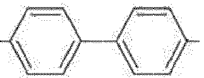
 n is a natural number of 2 to 5.
 - A method according to claim 12, wherein
the first alignment layer includes a first polymer, the first polymer includes a first main chain and a plurality of first side chains connected to the first main chain, and at least one among the plurality of first side chains includes a photoreactive group. - A method according to claim 13, wherein
the second alignment layer includes a second polymer, the second polymer includes a second main chain and a plurality of second side chains connected to the second main chain, and the plurality of second side chains do not include the photoreactive group. - A method according to any one of claims 12 to 14, wherein
the reactive mesogen is represented by Chemical Formula A or Chemical Formula B:

- A method according to any one of claims 12 to 15, wherein
among the plurality of protrusions, the density of the protrusions positioned between the first alignment layer and the liquid crystal layer is higher than the density of the protrusions positioned between the second alignment layer and the liquid crystal layer. - A method according to claim 16, wherein
the size of the protrusions positioned between the first alignment layer and the liquid crystal layer is smaller than the size of the protrusions positioned between the second alignment layer and the liquid crystal layer. - A method according to any one of claims 12 to 17, wherein
after the step of light irradiation, the pre-tilt angle of the liquid crystal molecules adjacent to the first alignment layer among the plurality of liquid crystal molecules is larger than the pre-tilt angle of the liquid crystal molecules adjacent to the second alignment layer among the plurality of liquid crystal molecules. - A method according to any one of claims 12 to 18, further comprising
providing a curved surface to the first substrate and the second substrate. - A liquid crystal display according to any one of claims 12 to 18, wherein
the first alignment layer is divided into a lower alignment layer and an upper alignment layer, a buffer region is formed between the lower alignment layer and the upper alignment layer,
the upper alignment layer includes a photoreactive group, the lower alignment layer does not include the photoreactive group, and the buffer region includes less of the photoreactive group than the content of the photoreactive group distributed in the upper alignment layer.
Applications Claiming Priority (1)
| Application Number | Priority Date | Filing Date | Title |
|---|---|---|---|
| KR1020160068898A KR102611868B1 (en) | 2016-06-02 | 2016-06-02 | Liquid crystal display and manufacturing method thereof |
Publications (3)
| Publication Number | Publication Date |
|---|---|
| EP3252528A2 true EP3252528A2 (en) | 2017-12-06 |
| EP3252528A3 EP3252528A3 (en) | 2017-12-20 |
| EP3252528B1 EP3252528B1 (en) | 2019-08-21 |
Family
ID=58992723
Family Applications (1)
| Application Number | Title | Priority Date | Filing Date |
|---|---|---|---|
| EP17174112.7A Active EP3252528B1 (en) | 2016-06-02 | 2017-06-01 | Liquid crystal display and manufacturing method thereof |
Country Status (4)
| Country | Link |
|---|---|
| US (1) | US10459291B2 (en) |
| EP (1) | EP3252528B1 (en) |
| KR (1) | KR102611868B1 (en) |
| CN (1) | CN107463028B (en) |
Family Cites Families (19)
| Publication number | Priority date | Publication date | Assignee | Title |
|---|---|---|---|---|
| DE602006012969D1 (en) | 2005-06-10 | 2010-04-29 | Merck Patent Gmbh | LIQUID CRYSTALLINE MATERIAL WITH HOMEOTROPER ORIENTATION |
| ATE547502T1 (en) | 2007-08-30 | 2012-03-15 | Merck Patent Gmbh | LIQUID CRYSTAL DISPLAY |
| US8114310B2 (en) | 2007-10-22 | 2012-02-14 | Merck Patent Gmbh | Liquid-crystal display |
| US8283000B2 (en) * | 2008-02-22 | 2012-10-09 | Adeka Corporation | Liquid crystal composition containing polymerizable compound and liquid crystal display using the liquid crystal composition |
| TWI452122B (en) | 2012-02-24 | 2014-09-11 | Dainippon Ink & Chemicals | Liquid crystal composition |
| KR101316708B1 (en) | 2012-04-26 | 2013-10-10 | 디아이씨 가부시끼가이샤 | Nematic liquid crystal composition and liquid crystal display device utilizing the same |
| CN102732265B (en) * | 2012-06-15 | 2014-04-09 | 深圳市华星光电技术有限公司 | Liquid crystal medium composition for liquid crystal display |
| CN102863968A (en) * | 2012-09-21 | 2013-01-09 | 深圳市华星光电技术有限公司 | Liquid crystal medium mixture and liquid crystal display using liquid crystal medium mixture |
| CN102888229B (en) * | 2012-09-21 | 2014-07-16 | 深圳市华星光电技术有限公司 | Liquid crystal medium mixture and liquid crystal display using same |
| KR102092942B1 (en) * | 2013-09-02 | 2020-03-25 | 삼성디스플레이 주식회사 | Liquid crystal display and method for manufacturing the same |
| US9720283B2 (en) * | 2014-02-26 | 2017-08-01 | Samsung Display Co., Ltd | Curved display device comprising first and second liquid crystal molecules with respective first and second pretilt-angles and method of manufacturing the same |
| US9671647B2 (en) * | 2014-03-31 | 2017-06-06 | Samsung Display Co., Ltd. | Curved display device |
| KR20150139430A (en) * | 2014-05-30 | 2015-12-11 | 주식회사 동진쎄미켐 | The novel bimesogenic compound |
| EP2963489B1 (en) * | 2014-06-30 | 2019-06-19 | Samsung Display Co., Ltd. | Curved display device |
| US9904113B2 (en) | 2014-07-30 | 2018-02-27 | Samsung Display Co., Ltd. | Alignment composition, liquid crystal display panel and method of manufacturing same |
| US20160032190A1 (en) | 2014-07-30 | 2016-02-04 | Samsung Display Co., Ltd. | Composition for aligning, display panel and method of manufacturing same |
| US10379408B2 (en) | 2014-11-05 | 2019-08-13 | Samsung Display Co., Ltd. | Curved display device |
| US9759948B2 (en) * | 2014-11-10 | 2017-09-12 | Samsung Display Co., Ltd. | Curved liquid crystal display |
| KR20170136029A (en) * | 2016-05-30 | 2017-12-11 | 삼성디스플레이 주식회사 | Liquid crystal display and manufacturing method thereof |
-
2016
- 2016-06-02 KR KR1020160068898A patent/KR102611868B1/en active Active
-
2017
- 2017-01-19 US US15/409,621 patent/US10459291B2/en active Active
- 2017-05-18 CN CN201710350350.4A patent/CN107463028B/en active Active
- 2017-06-01 EP EP17174112.7A patent/EP3252528B1/en active Active
Non-Patent Citations (1)
| Title |
|---|
| None |
Also Published As
| Publication number | Publication date |
|---|---|
| CN107463028B (en) | 2022-07-01 |
| KR102611868B1 (en) | 2023-12-11 |
| EP3252528A3 (en) | 2017-12-20 |
| CN107463028A (en) | 2017-12-12 |
| KR20170137264A (en) | 2017-12-13 |
| EP3252528B1 (en) | 2019-08-21 |
| US20170351146A1 (en) | 2017-12-07 |
| US10459291B2 (en) | 2019-10-29 |
Similar Documents
| Publication | Publication Date | Title |
|---|---|---|
| US8685502B2 (en) | Liquid crystal display | |
| US10985469B2 (en) | Scanning antenna and method for manufacturing same | |
| US7679713B2 (en) | Liquid crystal display device and manufacturing method thereof | |
| US10957990B2 (en) | Scanning antenna | |
| US10637156B2 (en) | Scanning antenna and method for manufacturing scanning antenna | |
| US20190229431A1 (en) | Scanning antenna and method of manufacturing scanning antenna | |
| KR20160053264A (en) | Compound for alignment layer, Alignment layer, Method of fabricating alignment layer and Liquid crystal display device including alignment layer | |
| US10756444B2 (en) | Scanning antenna and scanning antenna production method | |
| KR20170019544A (en) | Curved liquid crystal display and method for manufacturing the same | |
| KR20170030134A (en) | liquid crystal display | |
| EP2799517B1 (en) | Liquid crystal composition, liquid crystal display, and method of manufacturing liquid crystal display | |
| KR20170021940A (en) | Curved liquid crystal display and method for manufacturing the same | |
| US10847875B2 (en) | TFT substrate, scanning antenna provided with TFT substrate and method for producing TFT substrate | |
| KR20150034476A (en) | Liquid crystal photo alignment agent, liquid crystal display device including the same and method of manufacturing the same | |
| US11342666B2 (en) | TFT substrate, scanning antenna provided with TFT substrate, and method for manufacturing TFT substrate | |
| KR20170052742A (en) | Liquid crystal display device and method of manufacturing the same | |
| US10770792B2 (en) | Scanning antenna | |
| EP3252528B1 (en) | Liquid crystal display and manufacturing method thereof | |
| US10082706B2 (en) | Liquid crystal display device | |
| KR20170104079A (en) | Liquid crystal display and method of manufacturing the same | |
| US20160209708A1 (en) | Liquid crystal display and method of manufacturing the same | |
| KR20170019507A (en) | Curved liquid crystal display and method of manufacturing the same | |
| KR102449991B1 (en) | Curved liquid crystal display | |
| KR20170120222A (en) | Composition for alignment layer and liquid crystal display comprising the same and method for manufacturing the liquid crystal display | |
| KR20090051484A (en) | LCD and its manufacturing method |
Legal Events
| Date | Code | Title | Description |
|---|---|---|---|
| PUAI | Public reference made under article 153(3) epc to a published international application that has entered the european phase |
Free format text: ORIGINAL CODE: 0009012 |
|
| STAA | Information on the status of an ep patent application or granted ep patent |
Free format text: STATUS: THE APPLICATION HAS BEEN PUBLISHED |
|
| PUAL | Search report despatched |
Free format text: ORIGINAL CODE: 0009013 |
|
| AK | Designated contracting states |
Kind code of ref document: A2 Designated state(s): AL AT BE BG CH CY CZ DE DK EE ES FI FR GB GR HR HU IE IS IT LI LT LU LV MC MK MT NL NO PL PT RO RS SE SI SK SM TR |
|
| AX | Request for extension of the european patent |
Extension state: BA ME |
|
| AK | Designated contracting states |
Kind code of ref document: A3 Designated state(s): AL AT BE BG CH CY CZ DE DK EE ES FI FR GB GR HR HU IE IS IT LI LT LU LV MC MK MT NL NO PL PT RO RS SE SI SK SM TR |
|
| AX | Request for extension of the european patent |
Extension state: BA ME |
|
| RIC1 | Information provided on ipc code assigned before grant |
Ipc: G02F 1/1337 20060101AFI20171113BHEP |
|
| STAA | Information on the status of an ep patent application or granted ep patent |
Free format text: STATUS: REQUEST FOR EXAMINATION WAS MADE |
|
| 17P | Request for examination filed |
Effective date: 20180522 |
|
| RBV | Designated contracting states (corrected) |
Designated state(s): AL AT BE BG CH CY CZ DE DK EE ES FI FR GB GR HR HU IE IS IT LI LT LU LV MC MK MT NL NO PL PT RO RS SE SI SK SM TR |
|
| GRAP | Despatch of communication of intention to grant a patent |
Free format text: ORIGINAL CODE: EPIDOSNIGR1 |
|
| STAA | Information on the status of an ep patent application or granted ep patent |
Free format text: STATUS: GRANT OF PATENT IS INTENDED |
|
| INTG | Intention to grant announced |
Effective date: 20190328 |
|
| GRAS | Grant fee paid |
Free format text: ORIGINAL CODE: EPIDOSNIGR3 |
|
| GRAA | (expected) grant |
Free format text: ORIGINAL CODE: 0009210 |
|
| STAA | Information on the status of an ep patent application or granted ep patent |
Free format text: STATUS: THE PATENT HAS BEEN GRANTED |
|
| AK | Designated contracting states |
Kind code of ref document: B1 Designated state(s): AL AT BE BG CH CY CZ DE DK EE ES FI FR GB GR HR HU IE IS IT LI LT LU LV MC MK MT NL NO PL PT RO RS SE SI SK SM TR |
|
| REG | Reference to a national code |
Ref country code: GB Ref legal event code: FG4D |
|
| REG | Reference to a national code |
Ref country code: CH Ref legal event code: EP |
|
| REG | Reference to a national code |
Ref country code: DE Ref legal event code: R096 Ref document number: 602017006265 Country of ref document: DE |
|
| REG | Reference to a national code |
Ref country code: AT Ref legal event code: REF Ref document number: 1170414 Country of ref document: AT Kind code of ref document: T Effective date: 20190915 |
|
| REG | Reference to a national code |
Ref country code: IE Ref legal event code: FG4D |
|
| REG | Reference to a national code |
Ref country code: NL Ref legal event code: FP |
|
| REG | Reference to a national code |
Ref country code: LT Ref legal event code: MG4D |
|
| PG25 | Lapsed in a contracting state [announced via postgrant information from national office to epo] |
Ref country code: FI Free format text: LAPSE BECAUSE OF FAILURE TO SUBMIT A TRANSLATION OF THE DESCRIPTION OR TO PAY THE FEE WITHIN THE PRESCRIBED TIME-LIMIT Effective date: 20190821 Ref country code: HR Free format text: LAPSE BECAUSE OF FAILURE TO SUBMIT A TRANSLATION OF THE DESCRIPTION OR TO PAY THE FEE WITHIN THE PRESCRIBED TIME-LIMIT Effective date: 20190821 Ref country code: PT Free format text: LAPSE BECAUSE OF FAILURE TO SUBMIT A TRANSLATION OF THE DESCRIPTION OR TO PAY THE FEE WITHIN THE PRESCRIBED TIME-LIMIT Effective date: 20191223 Ref country code: NO Free format text: LAPSE BECAUSE OF FAILURE TO SUBMIT A TRANSLATION OF THE DESCRIPTION OR TO PAY THE FEE WITHIN THE PRESCRIBED TIME-LIMIT Effective date: 20191121 Ref country code: BG Free format text: LAPSE BECAUSE OF FAILURE TO SUBMIT A TRANSLATION OF THE DESCRIPTION OR TO PAY THE FEE WITHIN THE PRESCRIBED TIME-LIMIT Effective date: 20191121 Ref country code: SE Free format text: LAPSE BECAUSE OF FAILURE TO SUBMIT A TRANSLATION OF THE DESCRIPTION OR TO PAY THE FEE WITHIN THE PRESCRIBED TIME-LIMIT Effective date: 20190821 Ref country code: LT Free format text: LAPSE BECAUSE OF FAILURE TO SUBMIT A TRANSLATION OF THE DESCRIPTION OR TO PAY THE FEE WITHIN THE PRESCRIBED TIME-LIMIT Effective date: 20190821 |
|
| PG25 | Lapsed in a contracting state [announced via postgrant information from national office to epo] |
Ref country code: ES Free format text: LAPSE BECAUSE OF FAILURE TO SUBMIT A TRANSLATION OF THE DESCRIPTION OR TO PAY THE FEE WITHIN THE PRESCRIBED TIME-LIMIT Effective date: 20190821 Ref country code: GR Free format text: LAPSE BECAUSE OF FAILURE TO SUBMIT A TRANSLATION OF THE DESCRIPTION OR TO PAY THE FEE WITHIN THE PRESCRIBED TIME-LIMIT Effective date: 20191122 Ref country code: AL Free format text: LAPSE BECAUSE OF FAILURE TO SUBMIT A TRANSLATION OF THE DESCRIPTION OR TO PAY THE FEE WITHIN THE PRESCRIBED TIME-LIMIT Effective date: 20190821 Ref country code: LV Free format text: LAPSE BECAUSE OF FAILURE TO SUBMIT A TRANSLATION OF THE DESCRIPTION OR TO PAY THE FEE WITHIN THE PRESCRIBED TIME-LIMIT Effective date: 20190821 Ref country code: IS Free format text: LAPSE BECAUSE OF FAILURE TO SUBMIT A TRANSLATION OF THE DESCRIPTION OR TO PAY THE FEE WITHIN THE PRESCRIBED TIME-LIMIT Effective date: 20191221 Ref country code: RS Free format text: LAPSE BECAUSE OF FAILURE TO SUBMIT A TRANSLATION OF THE DESCRIPTION OR TO PAY THE FEE WITHIN THE PRESCRIBED TIME-LIMIT Effective date: 20190821 |
|
| REG | Reference to a national code |
Ref country code: AT Ref legal event code: MK05 Ref document number: 1170414 Country of ref document: AT Kind code of ref document: T Effective date: 20190821 |
|
| PG25 | Lapsed in a contracting state [announced via postgrant information from national office to epo] |
Ref country code: TR Free format text: LAPSE BECAUSE OF FAILURE TO SUBMIT A TRANSLATION OF THE DESCRIPTION OR TO PAY THE FEE WITHIN THE PRESCRIBED TIME-LIMIT Effective date: 20190821 |
|
| PG25 | Lapsed in a contracting state [announced via postgrant information from national office to epo] |
Ref country code: PL Free format text: LAPSE BECAUSE OF FAILURE TO SUBMIT A TRANSLATION OF THE DESCRIPTION OR TO PAY THE FEE WITHIN THE PRESCRIBED TIME-LIMIT Effective date: 20190821 Ref country code: EE Free format text: LAPSE BECAUSE OF FAILURE TO SUBMIT A TRANSLATION OF THE DESCRIPTION OR TO PAY THE FEE WITHIN THE PRESCRIBED TIME-LIMIT Effective date: 20190821 Ref country code: AT Free format text: LAPSE BECAUSE OF FAILURE TO SUBMIT A TRANSLATION OF THE DESCRIPTION OR TO PAY THE FEE WITHIN THE PRESCRIBED TIME-LIMIT Effective date: 20190821 Ref country code: RO Free format text: LAPSE BECAUSE OF FAILURE TO SUBMIT A TRANSLATION OF THE DESCRIPTION OR TO PAY THE FEE WITHIN THE PRESCRIBED TIME-LIMIT Effective date: 20190821 Ref country code: IT Free format text: LAPSE BECAUSE OF FAILURE TO SUBMIT A TRANSLATION OF THE DESCRIPTION OR TO PAY THE FEE WITHIN THE PRESCRIBED TIME-LIMIT Effective date: 20190821 Ref country code: DK Free format text: LAPSE BECAUSE OF FAILURE TO SUBMIT A TRANSLATION OF THE DESCRIPTION OR TO PAY THE FEE WITHIN THE PRESCRIBED TIME-LIMIT Effective date: 20190821 |
|
| PG25 | Lapsed in a contracting state [announced via postgrant information from national office to epo] |
Ref country code: CZ Free format text: LAPSE BECAUSE OF FAILURE TO SUBMIT A TRANSLATION OF THE DESCRIPTION OR TO PAY THE FEE WITHIN THE PRESCRIBED TIME-LIMIT Effective date: 20190821 Ref country code: SK Free format text: LAPSE BECAUSE OF FAILURE TO SUBMIT A TRANSLATION OF THE DESCRIPTION OR TO PAY THE FEE WITHIN THE PRESCRIBED TIME-LIMIT Effective date: 20190821 Ref country code: SM Free format text: LAPSE BECAUSE OF FAILURE TO SUBMIT A TRANSLATION OF THE DESCRIPTION OR TO PAY THE FEE WITHIN THE PRESCRIBED TIME-LIMIT Effective date: 20190821 Ref country code: IS Free format text: LAPSE BECAUSE OF FAILURE TO SUBMIT A TRANSLATION OF THE DESCRIPTION OR TO PAY THE FEE WITHIN THE PRESCRIBED TIME-LIMIT Effective date: 20200224 |
|
| REG | Reference to a national code |
Ref country code: DE Ref legal event code: R097 Ref document number: 602017006265 Country of ref document: DE |
|
| PLBE | No opposition filed within time limit |
Free format text: ORIGINAL CODE: 0009261 |
|
| STAA | Information on the status of an ep patent application or granted ep patent |
Free format text: STATUS: NO OPPOSITION FILED WITHIN TIME LIMIT |
|
| PG2D | Information on lapse in contracting state deleted |
Ref country code: IS |
|
| 26N | No opposition filed |
Effective date: 20200603 |
|
| PG25 | Lapsed in a contracting state [announced via postgrant information from national office to epo] |
Ref country code: SI Free format text: LAPSE BECAUSE OF FAILURE TO SUBMIT A TRANSLATION OF THE DESCRIPTION OR TO PAY THE FEE WITHIN THE PRESCRIBED TIME-LIMIT Effective date: 20190821 |
|
| PG25 | Lapsed in a contracting state [announced via postgrant information from national office to epo] |
Ref country code: MC Free format text: LAPSE BECAUSE OF FAILURE TO SUBMIT A TRANSLATION OF THE DESCRIPTION OR TO PAY THE FEE WITHIN THE PRESCRIBED TIME-LIMIT Effective date: 20190821 |
|
| REG | Reference to a national code |
Ref country code: CH Ref legal event code: PL |
|
| PG25 | Lapsed in a contracting state [announced via postgrant information from national office to epo] |
Ref country code: LU Free format text: LAPSE BECAUSE OF NON-PAYMENT OF DUE FEES Effective date: 20200601 |
|
| REG | Reference to a national code |
Ref country code: BE Ref legal event code: MM Effective date: 20200630 |
|
| PG25 | Lapsed in a contracting state [announced via postgrant information from national office to epo] |
Ref country code: IE Free format text: LAPSE BECAUSE OF NON-PAYMENT OF DUE FEES Effective date: 20200601 Ref country code: CH Free format text: LAPSE BECAUSE OF NON-PAYMENT OF DUE FEES Effective date: 20200630 Ref country code: LI Free format text: LAPSE BECAUSE OF NON-PAYMENT OF DUE FEES Effective date: 20200630 |
|
| PG25 | Lapsed in a contracting state [announced via postgrant information from national office to epo] |
Ref country code: BE Free format text: LAPSE BECAUSE OF NON-PAYMENT OF DUE FEES Effective date: 20200630 |
|
| PG25 | Lapsed in a contracting state [announced via postgrant information from national office to epo] |
Ref country code: MT Free format text: LAPSE BECAUSE OF FAILURE TO SUBMIT A TRANSLATION OF THE DESCRIPTION OR TO PAY THE FEE WITHIN THE PRESCRIBED TIME-LIMIT Effective date: 20190821 Ref country code: CY Free format text: LAPSE BECAUSE OF FAILURE TO SUBMIT A TRANSLATION OF THE DESCRIPTION OR TO PAY THE FEE WITHIN THE PRESCRIBED TIME-LIMIT Effective date: 20190821 |
|
| PG25 | Lapsed in a contracting state [announced via postgrant information from national office to epo] |
Ref country code: MK Free format text: LAPSE BECAUSE OF FAILURE TO SUBMIT A TRANSLATION OF THE DESCRIPTION OR TO PAY THE FEE WITHIN THE PRESCRIBED TIME-LIMIT Effective date: 20190821 |
|
| P01 | Opt-out of the competence of the unified patent court (upc) registered |
Effective date: 20230516 |
|
| PGFP | Annual fee paid to national office [announced via postgrant information from national office to epo] |
Ref country code: NL Payment date: 20250520 Year of fee payment: 9 |
|
| PGFP | Annual fee paid to national office [announced via postgrant information from national office to epo] |
Ref country code: DE Payment date: 20250520 Year of fee payment: 9 |
|
| PGFP | Annual fee paid to national office [announced via postgrant information from national office to epo] |
Ref country code: GB Payment date: 20250520 Year of fee payment: 9 |
|
| PGFP | Annual fee paid to national office [announced via postgrant information from national office to epo] |
Ref country code: FR Payment date: 20250521 Year of fee payment: 9 |