EP3249814A1 - A method for load measurement in switching amplifiers, corresponding device and amplifier - Google Patents
A method for load measurement in switching amplifiers, corresponding device and amplifier Download PDFInfo
- Publication number
- EP3249814A1 EP3249814A1 EP16206322.6A EP16206322A EP3249814A1 EP 3249814 A1 EP3249814 A1 EP 3249814A1 EP 16206322 A EP16206322 A EP 16206322A EP 3249814 A1 EP3249814 A1 EP 3249814A1
- Authority
- EP
- European Patent Office
- Prior art keywords
- amplifier
- differential
- output current
- common mode
- impedance
- Prior art date
- Legal status (The legal status is an assumption and is not a legal conclusion. Google has not performed a legal analysis and makes no representation as to the accuracy of the status listed.)
- Granted
Links
Images




Classifications
-
- H—ELECTRICITY
- H03—ELECTRONIC CIRCUITRY
- H03F—AMPLIFIERS
- H03F1/00—Details of amplifiers with only discharge tubes, only semiconductor devices or only unspecified devices as amplifying elements
- H03F1/08—Modifications of amplifiers to reduce detrimental influences of internal impedances of amplifying elements
- H03F1/083—Modifications of amplifiers to reduce detrimental influences of internal impedances of amplifying elements in transistor amplifiers
-
- G—PHYSICS
- G01—MEASURING; TESTING
- G01R—MEASURING ELECTRIC VARIABLES; MEASURING MAGNETIC VARIABLES
- G01R31/00—Arrangements for testing electric properties; Arrangements for locating electric faults; Arrangements for electrical testing characterised by what is being tested not provided for elsewhere
- G01R31/28—Testing of electronic circuits, e.g. by signal tracer
- G01R31/282—Testing of electronic circuits specially adapted for particular applications not provided for elsewhere
- G01R31/2825—Testing of electronic circuits specially adapted for particular applications not provided for elsewhere in household appliances or professional audio/video equipment
-
- H—ELECTRICITY
- H03—ELECTRONIC CIRCUITRY
- H03F—AMPLIFIERS
- H03F3/00—Amplifiers with only discharge tubes or only semiconductor devices as amplifying elements
- H03F3/181—Low-frequency amplifiers, e.g. audio preamplifiers
- H03F3/183—Low-frequency amplifiers, e.g. audio preamplifiers with semiconductor devices only
-
- H—ELECTRICITY
- H03—ELECTRONIC CIRCUITRY
- H03F—AMPLIFIERS
- H03F3/00—Amplifiers with only discharge tubes or only semiconductor devices as amplifying elements
- H03F3/20—Power amplifiers, e.g. Class B amplifiers, Class C amplifiers
- H03F3/21—Power amplifiers, e.g. Class B amplifiers, Class C amplifiers with semiconductor devices only
- H03F3/217—Class D power amplifiers; Switching amplifiers
-
- H—ELECTRICITY
- H03—ELECTRONIC CIRCUITRY
- H03F—AMPLIFIERS
- H03F3/00—Amplifiers with only discharge tubes or only semiconductor devices as amplifying elements
- H03F3/20—Power amplifiers, e.g. Class B amplifiers, Class C amplifiers
- H03F3/21—Power amplifiers, e.g. Class B amplifiers, Class C amplifiers with semiconductor devices only
- H03F3/217—Class D power amplifiers; Switching amplifiers
- H03F3/2173—Class D power amplifiers; Switching amplifiers of the bridge type
-
- H—ELECTRICITY
- H03—ELECTRONIC CIRCUITRY
- H03F—AMPLIFIERS
- H03F3/00—Amplifiers with only discharge tubes or only semiconductor devices as amplifying elements
- H03F3/45—Differential amplifiers
- H03F3/45071—Differential amplifiers with semiconductor devices only
-
- H—ELECTRICITY
- H03—ELECTRONIC CIRCUITRY
- H03F—AMPLIFIERS
- H03F3/00—Amplifiers with only discharge tubes or only semiconductor devices as amplifying elements
- H03F3/45—Differential amplifiers
- H03F3/45071—Differential amplifiers with semiconductor devices only
- H03F3/45076—Differential amplifiers with semiconductor devices only characterised by the way of implementation of the active amplifying circuit in the differential amplifier
- H03F3/45475—Differential amplifiers with semiconductor devices only characterised by the way of implementation of the active amplifying circuit in the differential amplifier using IC blocks as the active amplifying circuit
-
- H—ELECTRICITY
- H04—ELECTRIC COMMUNICATION TECHNIQUE
- H04R—LOUDSPEAKERS, MICROPHONES, GRAMOPHONE PICK-UPS OR LIKE ACOUSTIC ELECTROMECHANICAL TRANSDUCERS; ELECTRIC HEARING AIDS; PUBLIC ADDRESS SYSTEMS
- H04R29/00—Monitoring arrangements; Testing arrangements
- H04R29/001—Monitoring arrangements; Testing arrangements for loudspeakers
-
- H—ELECTRICITY
- H03—ELECTRONIC CIRCUITRY
- H03F—AMPLIFIERS
- H03F2200/00—Indexing scheme relating to amplifiers
- H03F2200/03—Indexing scheme relating to amplifiers the amplifier being designed for audio applications
-
- H—ELECTRICITY
- H03—ELECTRONIC CIRCUITRY
- H03F—AMPLIFIERS
- H03F2200/00—Indexing scheme relating to amplifiers
- H03F2200/171—A filter circuit coupled to the output of an amplifier
-
- H—ELECTRICITY
- H03—ELECTRONIC CIRCUITRY
- H03F—AMPLIFIERS
- H03F2200/00—Indexing scheme relating to amplifiers
- H03F2200/351—Pulse width modulation being used in an amplifying circuit
-
- H—ELECTRICITY
- H03—ELECTRONIC CIRCUITRY
- H03F—AMPLIFIERS
- H03F2200/00—Indexing scheme relating to amplifiers
- H03F2200/391—Indexing scheme relating to amplifiers the output circuit of an amplifying stage comprising an LC-network
-
- H—ELECTRICITY
- H03—ELECTRONIC CIRCUITRY
- H03F—AMPLIFIERS
- H03F2200/00—Indexing scheme relating to amplifiers
- H03F2200/393—A measuring circuit being coupled to the output of an amplifier
-
- H—ELECTRICITY
- H03—ELECTRONIC CIRCUITRY
- H03F—AMPLIFIERS
- H03F2200/00—Indexing scheme relating to amplifiers
- H03F2200/462—Indexing scheme relating to amplifiers the current being sensed
-
- H—ELECTRICITY
- H03—ELECTRONIC CIRCUITRY
- H03F—AMPLIFIERS
- H03F2203/00—Indexing scheme relating to amplifiers with only discharge tubes or only semiconductor devices as amplifying elements covered by H03F3/00
- H03F2203/45—Indexing scheme relating to differential amplifiers
- H03F2203/45008—Indexing scheme relating to differential amplifiers the addition of two signals being made by a resistor addition circuit for producing the common mode signal
-
- H—ELECTRICITY
- H03—ELECTRONIC CIRCUITRY
- H03F—AMPLIFIERS
- H03F2203/00—Indexing scheme relating to amplifiers with only discharge tubes or only semiconductor devices as amplifying elements covered by H03F3/00
- H03F2203/45—Indexing scheme relating to differential amplifiers
- H03F2203/45528—Indexing scheme relating to differential amplifiers the FBC comprising one or more passive resistors and being coupled between the LC and the IC
-
- H—ELECTRICITY
- H03—ELECTRONIC CIRCUITRY
- H03F—AMPLIFIERS
- H03F2203/00—Indexing scheme relating to amplifiers with only discharge tubes or only semiconductor devices as amplifying elements covered by H03F3/00
- H03F2203/45—Indexing scheme relating to differential amplifiers
- H03F2203/45631—Indexing scheme relating to differential amplifiers the LC comprising one or more capacitors, e.g. coupling capacitors
Definitions
- the description relates to load measurement in amplifiers.
- One or more embodiments may apply to high-frequency load measurement in high-frequency switching amplifiers.
- So-called class D audio amplifiers may be exemplary of such amplifiers.
- the need may arise of monitoring/measuring an otherwise unknown load driven by a switching (e.g. class D) amplifier and/or by monitoring/measuring a passive LC filter and dumping network impedance without disconnecting the load.
- a switching e.g. class D
- various application may involve performing AC current sensing in an audio (e.g. two-way) speaker system driven by a class D amplifier for diagnostic purposes, for instance.
- an audio e.g. two-way
- a class D amplifier for diagnostic purposes, for instance.
- An object of one or more embodiments is to provide a solution for AC load diagnostics and passive filter network diagnostics-metering for use e.g. in standard bridge-type class D amplifiers, e.g. without feedback after the LC demodulator filter.
- One or more embodiments may relate to a corresponding system and corresponding apparatus (e.g. a switching amplifier such a class D amplifier).
- a switching amplifier such as a class D amplifier
- references to "an embodiment” or “one embodiment” in the framework of the present description is intended to indicate a particular configuration, structure, characteristic described in relation to the embodiment is compliance in at least one embodiment.
- phrases such as “in an embodiment” or “in one (or more) embodiments” that may be present in one or more points in the present description do not necessarily refer to one and the same embodiment.
- particular conformation, structures or characteristics as exemplified in connection with any of the figures may be combined in any other quite way in one or more embodiments as possibly exemplified in other figures.
- Figure 1 is a schematic representation of an amplifier A driving a load LS.
- a multi-way audio loudspeaker system may be exemplary of such a load.
- such a load may include a first loudspeaker (or “woofer”) WF and a second loudspeaker (or “tweeter”) TW for reproducing the low portion and the high portion of the audio frequency range (notionally 20Hz to 20kHz), respectively.
- a first loudspeaker or "woofer”
- a second loudspeaker or “tweeter”
- TW for reproducing the low portion and the high portion of the audio frequency range (notionally 20Hz to 20kHz), respectively.
- a wide variety of technologies may be applied in manufacturing the loudspeakers WF and TW.
- the amplifier A may feed the load with an output voltage V amp and an output current i amp .
- a so-called "crossover" network CN may partition the current i amp in a low-frequency component to the woofer WF and a high-frequency component to the tweeter TW, indicated i woofer and i tweeter respectively.
- a wide variety of crossover arrangements are known in the art.
- a crossover arrangement including an inductor L W and a capacitor CT coupled in series to the woofer WF and the tweeter T W is exemplified here for the sake of simplicity
- the need may arise of discriminating (e.g. on the basis of V amp and/or i amp ) between a normal tweeter condition, and an unconnected tweeter condition due to cabling being interrupted or the tweeter TW being inoperative, e.g. following the tweeter being "blown" by excessive power being fed thereto.
- performing such a task may take into account various factors such as:
- Performing such a function in a conventional (linear) amplifier may rely on the fact that the output voltage and current from the amplifier A may equal the voltage and current applied to the load LS.
- a switching (e.g. class D) amplifier things may be different insofar as the presence of an LC demodulator filter at the amplifier output leads to a situation where - even in the audio band - the load voltage and current may not correspond to the output voltage/current from the amplifier A.
- the values for L and C may have a certain tolerance (e.g. ⁇ 20%), which makes it hardly feasible to evaluate the load even in the presence of a precise current measurement.
- V load V amp ( 1 / 1 + j ⁇ L / R / 2 ⁇ ⁇ 2 LC
- I R V amp / R / 2 ( 1 / 1 + j ⁇ L / R / 2 ⁇ ⁇ 2 LC
- the values for L, C and the load impedance values may represent variables to be measured (for instance in order to equalize system frequency response).
- Such an arrangement may be used in the case of a full bridge PWM (class D) amplifier using two distinct single-ended branches and feedback applied after the inductor filter, so that single-ended driving can be easily applied with the frequency response of the output voltage V out essentially load-independent.
- a full bridge PWM (class D) amplifier using two distinct single-ended branches and feedback applied after the inductor filter, so that single-ended driving can be easily applied with the frequency response of the output voltage V out essentially load-independent.
- reference 10 denotes a (fully differential) amplifier arrangement including a basic switching (class D) amplifier circuit coupled with PWM (Pulse Width Modulation) modulators 12a, 12b with associated LC demodulator filters 14a, 16a and 14b, 16b having a common-mode (high impedance) sensing network 18a, 18b to provide a feedback signal to the amplifier 10 over a common mode feedback line 20.
- PWM Pulse Width Modulation
- Input to such a amplifier arrangement may be applied differentially (e.g. V in+ , V in- ).
- input resistors 22a, 22b which may be used e.g. for systems DC-coupled with a voltage source.
- a high-pass voltage input may be resorted to: in that case the elements exemplified here as the resistors 22a, 22b may be an impedance including a RC network.
- the differential input may be via an array of current generators.
- impedances 24a, 24b and 26a, 26b may provide feedback towards the input of the amplifier core 10:
- One or more embodiments may involve the use of a measuring system MS configured to co-operate with a class D amplifier by sensing/measuring certain electrical parameters and calculating certain values as discussed in the following.
- the measuring system MS may be external to the amplifier.
- the measuring system MS may be "on-board" the amplifier, that is at least partly incorporated to the amplifier.
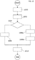
- the measuring system MS may be configured for operating according to the flow-chart exemplified in Figure 12 .
- One or more embodiments will make it possible to provide an effective AC load and LC network impedance measurement (also) for a class D amplifier system possibly having a no-single ended driving possibility: this may be the case of fully-differential system configurations wherein feedback is from upstream (namely from "before") the LC demodulator filter.
- the common-mode control circuit may be resorted to support operation as discussed in the following in connections with the exemplary flow- chart of Figure 12 .
- the AC output current magnitude and phase may be sensed (e.g. by the measuring system MS - in a manner known per se) while driving the amplifier in default conditions, namely differentially via the inputs V in+ , V in- .
- the AC output current magnitude and phase may be sensed while AC driving the amplifier in a common mode fashion (that is by applying a same signal to both inputs V in+ , V in- ).
- AC driving may be in both cases (differential/common-mode) in the upper portion (high frequency) the audio frequency range e.g. at about 20kHz, which may make such testing practically inaudible for the system user.
- step 1004 a distinction may be made between cases where feedback after the LC filter may apply (see e.g. Figure 2 ) from those cases where (standard) feedback before the LC filter may apply (see e.g. Figure 6 ).
- the evaluation of the load current and its impedance may include a further step 1008a involving measuring the value of an inductance by a ripple current measurement, namely a higher frequency AC common mode measurement before the load impedance may be evaluated in a step 1008b.
- an evaluation of the load current and its impedance may be performed even in the most general case of feedback before the LC demodulator filter (e.g. Figure 6 ).
- the impedance value of other passive filter components may be obtained from the measurements.
- other passive filter components e.g. a dumping network 30 coupled parallel to the capacitor 16a, 16b of the LC demodulator filter
- such a dumping network 30 may include a parallel connection of a resistor and two capacitors. While the individual values of such components may not be determined, evaluating the overall impedance may by itself represent a satisfactory result.
- the RC dumping network 30 cascaded to the LC demodulator filter 14a, 16a; 14b, 16b of the class D amplifier may be represented as a symmetrical network including two impedances Z c having an intermediate point set to ground, thus leading to an arrangement where one "half bridge" is equal to the other.
- the (high impedance) common-mode feedback circuit 18a, 18b can be driven by means of an AC signal (in the place of a DC fixed signal), which is possible in the case of a fully differential architecture as exemplified in Figures 2 and 6 .
- the output load voltage may be AC controlled and made known at e.g. 20 kHz ("high frequency" within the context of the present invention, when applied to audio systems).
- the load LS is essentially constituted by the tweeter TW (see Figure 1 ) in so far as the crossover network CN operates in such way that no appreciable current i woofer flows through the inductor L W and the woofer loudspeaker WF.
- proper feedback signal management may render the output load voltage v o (differential and common-mode) AC controllable and known at a high frequency, thus reducing frequency response dependence on load impedance.
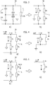
- Figures 4 and 5 are exemplary of the arrangement of Figure 2 being AC driven in a differential mode ( Figure 4 ) and in a common mode ( Figure 5 ), with differential driving being representative of a "default" driving mode of the amplifier between the input terminal V in+ and V in- .
- Sensing/measurement by the measuring system MS (involving voltmetric and amperometric modules - of a known type - not visible in the figures) will thus involve both magnitude (modulus) and phase (angle), this being the case also for the associated calculation steps.
- Figures 7 to 11 are exemplary of corresponding measuring steps which may be performed in the case of a circuit arrangement as exemplified in Figure 6 , that is with feedback obtained via the impedances 24a, 24b (only) before, that is upstream, of the LC demodulator filter 14a, 16a; 14b, 16b.
- the frequency response of the output voltage may be load-dependent.
- the AC voltage upstream of the LC demodulator filter may be known both in the case of differential driving and in the case of common mode driving.
- the same symmetrical modeling of the dumping network 30 and the load LS may be adopted e.g. by modeling the dumping network and the load as two symmetric impedances Z c and Z 0 .
- This resistive component may be in the range of a few tenth mOhm, and may thus be neglected or assumed to have a (very small) constant value.
- Figure 8 is exemplary of differentially driving (default driving) the amplifier arrangement of Figure 6 while sensing the output current i diff (both in magnitude and phase).
- the amplifier arrangement of Figure 6 may be driven in a common mode while sensing the output current i comm .
- the following relationship will thus apply:
- the inductive value (that is, L) of the inductor 14a, 14b of the LC demodulator filter may be largely dominant at a high frequency (e.g. 20 kHz) and may be evaluated with an AC frequency measurement. In one or more embodiments this may turn out to be somehow critical in view of the PWM limited high frequency response.
- this issue - namely measuring L - may be addressed by noting that in a switching (e.g. class D) amplifier driven with in-phase modulation, the current ripple at steady state, with no input signal (duty cycle set to 50%) may admit a first order approximation as a triangular wave having an amplitude I R which is (approximately) equal to: VCC / 2. L . f PWM where, as schematically shown in the upper portion of Figure 11 , VCC indicates the PWM output voltage (e.g. the output voltage of the PWM modulators 12a, 12b driven with 50% duty cycle) at a frequency f PWM .
- VCC indicates the PWM output voltage (e.g. the output voltage of the PWM modulators 12a, 12b driven with 50% duty cycle) at a frequency f PWM .
- Such a measurement may be performed, e.g. in the step exemplified as 1008a in figure 12 .
- a measuring system MS as exemplified e.g. in Figures 2 and 6 may be implemented according to the general layout exemplified by the block diagram of Figure 13 , where the following block designations apply:
- the voltage Vds may be ADC converted when the power stage is on, so that Vds ⁇ RdsON * Iload, by neglecting minor secondary effects.
- Another option may be direct measurement of Iout by Hall effect in the silicon.
- Sensing external to the amplifier may rely on the series resistance of the inductor by accessing the voltage before an after the filter.
- Arranging a sensing resistor Rsens in series to the load LS may reduce load swing and increase power dissipation, the same applying also to other current probes measuring the current on the load, which would result in a more complex system (including external components and/or additional pins in the IC).
- the tolerances indicated may only consider a component maximum variation without considering measurement error. It will be appreciated that, under such conditions, open load may not be detectable and might be done only to LC filter tolerance. For instance, at e.g. 20kHz with connected load, L and C at nominal value (no error), a current measured may be e.g. 0.88A. A same measured value may be obtained with a disconnected tweeter and a lower filter capacitance C: when the tweeter is disconnected, the load measurement may be largely influenced by the values of L and C which may vary extensively forma production item to another.
- Both typical values for L and C may be considered in a measurement which is not dependent on L and C tolerances as these are included in the quantities measured: that is, no a priori knowledge of L and C is needed since these may be measured in one or more embodiments. Open load conditions may thus be detected while also providing impedance evaluation.
- the measurement system MS may be incorporated to the amplifier circuitry, with the whole system adapted to be switched to "diagnostic" mode.
- the amplifier will be configured in order to operate, in addition to an otherwise standard AC differential mode (default mode - step 1000 in Figure 12 ) to an AC common mode in order to perform the step indicated as 1002 in Figure 12 .
Landscapes
- Engineering & Computer Science (AREA)
- Power Engineering (AREA)
- Physics & Mathematics (AREA)
- Multimedia (AREA)
- Health & Medical Sciences (AREA)
- General Physics & Mathematics (AREA)
- General Engineering & Computer Science (AREA)
- General Health & Medical Sciences (AREA)
- Otolaryngology (AREA)
- Acoustics & Sound (AREA)
- Signal Processing (AREA)
- Amplifiers (AREA)
- Arrangements For Transmission Of Measured Signals (AREA)
- Testing Electric Properties And Detecting Electric Faults (AREA)
Abstract
- AC driving (1000) the amplifier in a differential mode by applying a differential AC signal to the differential input and sensing the output current from the amplifier while driving the amplifier in the differential mode,
- AC driving (1002) the amplifier in a common mode by applying a common mode AC signal to the differential input and sensing the AC output current from the amplifier while driving the amplifier in the common mode, and
a) with the feedback network providing feedback towards said differential input from downstream the LC demodulator filter, computing (1006) the impedance of the load as a function of the differential mode output current and the common mode output current,
b) with the feedback network providing feedback towards the differential input from upstream the LC demodulator filter, measuring (1008a) the impedance value of the inductor of the LC demodulator filter, and computing (1008b) the impedance of the load as a function of the differential mode output current, the common mode output current and the impedance value of the inductor of the LC demodulator filter.
Description
- The description relates to load measurement in amplifiers.
- One or more embodiments may apply to high-frequency load measurement in high-frequency switching amplifiers. So-called class D audio amplifiers may be exemplary of such amplifiers.
- In various applications, the need may arise of monitoring/measuring an otherwise unknown load driven by a switching (e.g. class D) amplifier and/or by monitoring/measuring a passive LC filter and dumping network impedance without disconnecting the load.
- More specifically, various application may involve performing AC current sensing in an audio (e.g. two-way) speaker system driven by a class D amplifier for diagnostic purposes, for instance.
- An object of one or more embodiments is to provide a solution for AC load diagnostics and passive filter network diagnostics-metering for use e.g. in standard bridge-type class D amplifiers, e.g. without feedback after the LC demodulator filter.
- According to one or more embodiments, that object may be achieved by means of a method having the features set forth in the claims that follow.
- One or more embodiments may relate to a corresponding system and corresponding apparatus (e.g. a switching amplifier such a class D amplifier).
- One or more embodiments may offer one or more of the following advantages:
- embodiments may apply even when single-ended driving is not possible and with feedback before the LC demodulation filter;
- common mode driving may open new possibilities e.g. in terms of new diagnostic features.
- One or more embodiments will be described, by way of example only, with reference to the annexed figures, wherein:
-
Figure 1 is a schematic representation of an amplifier driving a load such as a 2-way speaker, -
Figure 2 is exemplary of one or more embodiments, -
Figures 3 to 5 , each including two portions indicated a) and b), respectively, are exemplary of possible operation of one or more embodiments, -
Figure 6 is exemplary of one or more embodiments, -
Figures 7 to 10 , each including two portions indicated a) and b), respectively, andFigure 11 are exemplary of possible operation of one or more embodiments, -
Figure 12 is a flow chart exemplary of one or more embodiments, and -
Figure 13 is an exemplary block diagram of embodiments of a measuring system. - In the ensuing description, one or more specific details are illustrated, aimed providing an in-depth understanding of examples of embodiments of the instant description. The embodiments may be obtained by one or more of the specific details or with other methods, components, materials, and so on. In other cases, known structures, materials or operations are not illustrated or described in detail so that certain aspects of embodiment will not be obscured.
- Reference to "an embodiment" or "one embodiment" in the framework of the present description is intended to indicate a particular configuration, structure, characteristic described in relation to the embodiment is compliance in at least one embodiment. Hence, phrases such as "in an embodiment" or "in one (or more) embodiments" that may be present in one or more points in the present description do not necessarily refer to one and the same embodiment. Moreover, particular conformation, structures or characteristics as exemplified in connection with any of the figures may be combined in any other quite way in one or more embodiments as possibly exemplified in other figures.
- The references used herein are provided merely for convenience and hence do not define the extent of protection or the scope of the embodiments.
-
Figure 1 is a schematic representation of an amplifier A driving a load LS. - A multi-way audio loudspeaker system may be exemplary of such a load.
- In the case of a two-way system as exemplified herein, such a load may include a first loudspeaker (or "woofer") WF and a second loudspeaker (or "tweeter") TW for reproducing the low portion and the high portion of the audio frequency range (notionally 20Hz to 20kHz), respectively. A wide variety of technologies (electrodynamic, piezoelectric, electrostatic, ribbon, and so on) may be applied in manufacturing the loudspeakers WF and TW.
- In driving the load LS the amplifier A may feed the load with an output voltage Vamp and an output current iamp. A so-called "crossover" network CN may partition the current iamp in a low-frequency component to the woofer WF and a high-frequency component to the tweeter TW, indicated iwoofer and itweeter respectively. A wide variety of crossover arrangements are known in the art. A crossover arrangement including an inductor LW and a capacitor CT coupled in series to the woofer WF and the tweeter TW is exemplified here for the sake of simplicity
- In various applications the need may arise of discriminating (e.g. on the basis of Vamp and/or iamp) between a normal tweeter condition, and an unconnected tweeter condition due to cabling being interrupted or the tweeter TW being inoperative, e.g. following the tweeter being "blown" by excessive power being fed thereto.
- In various applications, performing such a task may take into account various factors such as:
- in certain arrangements, the amplifier output current iamp may be measured (only) within the amplifier without relying on external shunt resistors,
- the parameters of the crossover network CN, e.g. the values for LW and CT in
Figure 1 may vary within a certain tolerance range (e.g. ± 10%). - Performing such a function in a conventional (linear) amplifier may rely on the fact that the output voltage and current from the amplifier A may equal the voltage and current applied to the load LS.
- In a switching (e.g. class D) amplifier things may be different insofar as the presence of an LC demodulator filter at the amplifier output leads to a situation where - even in the audio band - the load voltage and current may not correspond to the output voltage/current from the amplifier A.
- In fact the values for L and C may have a certain tolerance (e.g. ± 20%), which makes it hardly feasible to evaluate the load even in the presence of a precise current measurement.
- For instance, even assuming that the load LS may be modeled simply as a resistor R, the following relationships may apply:


- Vload and Vamp denote the voltage on the load and the amplifier output voltage, respectively;
- IR is the current through the load (resistor R)
- L and C are the inductance and capacitance value representative of the LC demodulator filter at the amplifier output, and
- ω is the "pulsation", representative of the frequency f, with ω = 2nf.
- In certain applications the values for L, C and the load impedance values may represent variables to be measured (for instance in order to equalize system frequency response).
- Document
US 2009/097667 A1 discloses a method and circuit for testing an audio high-frequency loudspeaker which is a part of a loudspeaker system. Such a document discloses two implementations involving single-ended driving (by keeping one of the input terminals to a virtual DC level) and the use of feedback both before and after the LC demodulator filter). In the former case, the measurement result is inaccurate, even though more precise that in the case that no single-ended driving is adopted. - While effective, the arrangement disclosed in such prior art document may exhibit certain limitations in terms of the architectures to which such solution may apply.
- For instance such an arrangement may be used in the case of a full bridge PWM (class D) amplifier using two distinct single-ended branches and feedback applied after the inductor filter, so that single-ended driving can be easily applied with the frequency response of the output voltage Vout essentially load-independent.
- Conversely, the solution disclosed in the document captioned in the foregoing may not be applicable in the case of a full-bridge PWM arrangement using a fully differential topology and feedback before the LC demodulator filter. In that case, single-ended driving of the output may be difficult to apply. Also, the frequency response of the output voltage Vout may be load-dependent (not equalized).
- In the diagram of
Figure 2 ,reference 10 denotes a (fully differential) amplifier arrangement including a basic switching (class D) amplifier circuit coupled with PWM (Pulse Width Modulation)modulators LC demodulator filters sensing network amplifier 10 over a commonmode feedback line 20. - Input to such a amplifier arrangement may be applied differentially (e.g. Vin+, Vin-).
- This may occur, as exemplified herein, via
input resistors - In other arrangements, a high-pass voltage input may be resorted to: in that case the elements exemplified here as the
resistors - In one or more embodiments,
impedances - via the
impedances PWM modulators inductor - via the
impedances - Further details on such an arrangement may be derived e.g. from
US 2007/0229155 A1 . - The description provided in the foregoing may also apply to the basic switching (class D) amplifier circuit illustrated in
Figure 6 , save that - in the case exemplified inFigure 6 - feedback towards the input of theamplifier core 10 may be provided (only) via theimpedances PWM modulators - One or more embodiments may involve the use of a measuring system MS configured to co-operate with a class D amplifier by sensing/measuring certain electrical parameters and calculating certain values as discussed in the following.
- In one or more embodiments, the measuring system MS may be external to the amplifier.
- In one or more embodiments the measuring system MS may be "on-board" the amplifier, that is at least partly incorporated to the amplifier.
- In one or more embodiments, the measuring system MS may be configured for operating according to the flow-chart exemplified in
Figure 12 . - A possible exemplary embodiment of such a measuring system will be discussed in the following in connection with
Figure 13 . - One or more embodiments will make it possible to provide an effective AC load and LC network impedance measurement (also) for a class D amplifier system possibly having a no-single ended driving possibility: this may be the case of fully-differential system configurations wherein feedback is from upstream (namely from "before") the LC demodulator filter.
- In one or more embodiments, the common-mode control circuit may be resorted to support operation as discussed in the following in connections with the exemplary flow- chart of
Figure 12 . - After a START step, in a
step 1000 the AC output current magnitude and phase may be sensed (e.g. by the measuring system MS - in a manner known per se) while driving the amplifier in default conditions, namely differentially via the inputs Vin+, Vin-. - In a
step 1002, the AC output current magnitude and phase may be sensed while AC driving the amplifier in a common mode fashion (that is by applying a same signal to both inputs Vin+, Vin-). - If high frequency measurement/monitoring is contemplated (e.g. in the higher portion of the audio frequency range covered by a tweeter TW as exemplified in
Figure 1 ) AC driving may be in both cases (differential/common-mode) in the upper portion (high frequency) the audio frequency range e.g. at about 20kHz, which may make such testing practically inaudible for the system user. - Subsequently (as exemplified by step 1004) a distinction may be made between cases where feedback after the LC filter may apply (see e.g.
Figure 2 ) from those cases where (standard) feedback before the LC filter may apply (see e.g.Figure 6 ). - In the former case (
Figure 2 ) evaluation of the load current and its impedance may take place in astep 1006 already on the basis of the differential and common-mode AC driving ofsteps - In the latter case (
Figure 6 ) the evaluation of the load current and its impedance may include afurther step 1008a involving measuring the value of an inductance by a ripple current measurement, namely a higher frequency AC common mode measurement before the load impedance may be evaluated in astep 1008b. - In one or more embodiments, an evaluation of the load current and its impedance may be performed even in the most general case of feedback before the LC demodulator filter (e.g.
Figure 6 ). - In one or more embodiments, the impedance value of other passive filter components (e.g. a dumping
network 30 coupled parallel to thecapacitor - In fact, such a
dumping network 30 may include a parallel connection of a resistor and two capacitors. While the individual values of such components may not be determined, evaluating the overall impedance may by itself represent a satisfactory result. - In the following, possible operation in the case where feedback after the LC demodulation filter may apply (
impedances Figure 2 ) will be exemplified with reference of the sequence ofsteps Figure 12 . - Then possible operation in the case where feedback before the LC demodulation filter may apply (
impedances Figure 6 ) will be exemplified with reference of the sequence ofsteps Figure 12 . - For the sake of simplicity, as exemplified in
Figure 3 , theRC dumping network 30 cascaded to theLC demodulator filter - Also, the (high impedance) common-
mode feedback circuit Figures 2 and6 . Also, one may assume that the output load voltage (differential and common mode) may be AC controlled and made known at e.g. 20 kHz ("high frequency" within the context of the present invention, when applied to audio systems). - In these conditions, one may assume that the load LS is essentially constituted by the tweeter TW (see
Figure 1 ) in so far as the crossover network CN operates in such way that no appreciable current iwoofer flows through the inductor LW and the woofer loudspeaker WF. - In one or more embodiments, proper feedback signal management (according to known principles) may render the output load voltage vo (differential and common-mode) AC controllable and known at a high frequency, thus reducing frequency response dependence on load impedance.
-
Figures 4 and 5 are exemplary of the arrangement ofFigure 2 being AC driven in a differential mode (Figure 4 ) and in a common mode (Figure 5 ), with differential driving being representative of a "default" driving mode of the amplifier between the input terminal Vin+ and Vin-. - In the case of differential AC driving (see
Figure 4 ), the following relationship applies:
- vo is the differential output voltage (+vo, -vo),
- idiff is output current sensed.
- In the case of common-mode AC driving, the following relationship applies:

- vo is the differential output voltage (+vo, -vo),
- icomm is output current sensed.
- By combining the two previous relationships, as derived during AC differential and common-mode driving (
steps Figure 12 ) the following relationship may be derived:
- In that way, both the load impedance Z0 (specifically LS = 2.Z0) and the impedance Zc of the dumping
network 30 may be derived and the result(s) made available in astep 1010. - While complex number notation is avoided here for the sake of simplicity, it will be appreciated that the electrical parameters discussed above are complex parameters.
- Sensing/measurement by the measuring system MS (involving voltmetric and amperometric modules - of a known type - not visible in the figures) will thus involve both magnitude (modulus) and phase (angle), this being the case also for the associated calculation steps.
-
Figures 7 to 11 are exemplary of corresponding measuring steps which may be performed in the case of a circuit arrangement as exemplified inFigure 6 , that is with feedback obtained via theimpedances LC demodulator filter - In such a case the frequency response of the output voltage may be load-dependent. Even in the case of
Figure 6 , however, the AC voltage upstream of the LC demodulator filter may be known both in the case of differential driving and in the case of common mode driving. - As schematically represented in
Figure 7 , the same symmetrical modeling of the dumpingnetwork 30 and the load LS may be adopted e.g. by modeling the dumping network and the load as two symmetric impedances Zc and Z0. - Also, for the sake of the following discussion, the inductor/
inductance - Again,
Figure 8 is exemplary of differentially driving (default driving) the amplifier arrangement ofFigure 6 while sensing the output current idiff (both in magnitude and phase). - Under these conditions (
step 1000 ofFigure 12 ) the following relationship will apply:
- Then (see
e.g. step 1002 inFigure 12 ) the amplifier arrangement ofFigure 6 may be driven in a common mode while sensing the output current icomm. The following relationship will thus apply: - vo/icomm = ZL + Zc, that is Zc = vo/icomm - ZL.
- In the case of the arrangement of
Figure 6 , the inductive value (that is, L) of theinductor - In one or more embodiments, this issue - namely measuring L - may be addressed by noting that in a switching (e.g. class D) amplifier driven with in-phase modulation, the current ripple at steady state, with no input signal (duty cycle set to 50%) may admit a first order approximation as a triangular wave having an amplitude IR which is (approximately) equal to:

Figure 11 , VCC indicates the PWM output voltage (e.g. the output voltage of thePWM modulators - Under these circumstances, as schematically shown in the lower portion of
Figure 11 , the inductance L may be measured by sampling the difference ΔI between the values taken of the current entering the PWM power stages at two different instants separated by a time Δt, namely:
- Such a measurement may be performed, e.g. in the step exemplified as 1008a in
figure 12 . - Consequently, the various measurements performed in the foregoing may be combined (e.g. in a
step 1008b) as exemplified in the following, so that both Zc and Z0 may be evaluated as

- In that way, both the load impedance Z0 (specifically LS = 2.Z0) and the impedance Zc of the dumping
network 30 may be derived and the result(s) may be made available in astep 1010. - While complex number notation is again avoided here for the sake of simplicity, it will once more be appreciated that the electrical parameters discussed above are complex parameters. Sensing/measurement by the measuring system MS (involving voltmetric and amperometric modules - of a known type - not visible in the figures) will thus involve both magnitude (modulus) and phase (angle), this being the case also for the associated calculation steps.
- In more embodiments, a measuring system MS as exemplified e.g. in
Figures 2 and6 may be implemented according to the general layout exemplified by the block diagram ofFigure 13 , where the following block designations apply: - 10 - Class D amplifier core (see also
Figures 2 and6 ) - 100 - State machine (main blocks handling)
- 102 - analog-to-digital converter (ADC) of the current i(t) from the amplifier
- 104 - sinusoid (sine-wave) generator
- 106 - digital-to-analog converter (DAC) of the sine-wave to the
amplifier 10 - 108 - magnitude (imag) and phase (iphase) evaluation block
- 110 - state machine for impedance evaluation based on imag and iphase
- 112 - arithmetic unit (including e.g. a multiplier X * Y, an inverse calculation module 1/X and a magnitude-phase <-> real(Re)-imaginary(Im) conversion module).
- 114 - memory
- In one or meme embodiments, various options may be adopted for signal sensing/detection.
- For instance, since a switching (class D) amplifier is involved one may rely on the "on" resistance RdsON of the power stage: the voltage Vds may be ADC converted when the power stage is on, so that Vds ≅ RdsON * Iload, by neglecting minor secondary effects.
- Another option may be direct measurement of Iout by Hall effect in the silicon.
- Sensing external to the amplifier may rely on the series resistance of the inductor by accessing the voltage before an after the filter.
- Arranging a sensing resistor Rsens in series to the load LS may reduce load swing and increase power dissipation, the same applying also to other current probes measuring the current on the load, which would result in a more complex system (including external components and/or additional pins in the IC).
- In a possible (real world) arrangement, the following values may be assumed:
-
inductors 
-
capacitors - resistor of the dumping network 30: Rd = 10 Ohm
- capacitor of the dumping network 30: Cd = 1 µF
- nominal (normal) load = 4 ohm
- open load = 4 Ohm + 600 µH = 75 Ohm 87 deg, when measurement is performed at 20 kHz.
- In a standard method, where only current magnitude is measured, values for the load current may be, e.g. i = 0.88 A ± 2% and i = 0.96 A ± 30%, in normal load condition and open load condition, respectively.
- The tolerances indicated may only consider a component maximum variation without considering measurement error. It will be appreciated that, under such conditions, open load may not be detectable and might be done only to LC filter tolerance. For instance, at e.g. 20kHz with connected load, L and C at nominal value (no error), a current measured may be e.g. 0.88A. A same measured value may be obtained with a disconnected tweeter and a lower filter capacitance C: when the tweeter is disconnected, the load measurement may be largely influenced by the values of L and C which may vary extensively forma production item to another.
- By using the solution of one or more embodiments, under the conditions outlined, and by assuming an even more critical situation (that is by assuming measurements of i and v affected by a 10% tolerance/error) a normal load having a module |Z| = 4 Ohm ± 15% and a phase = 0 ± 9 degrees may be detected.
- Similarly, in an open load condition, a module |Z| = 75 Ohm ± 16% and a phase = 87 ± 2 degrees may be detected by assuming as a
tolerance 10% error on current and inductance (this being likely to represent a worst case correlation). - Both typical values for L and C may be considered in a measurement which is not dependent on L and C tolerances as these are included in the quantities measured: that is, no a priori knowledge of L and C is needed since these may be measured in one or more embodiments. Open load conditions may thus be detected while also providing impedance evaluation.
- As indicated, in one or more embodiments, the measurement system MS may be incorporated to the amplifier circuitry, with the whole system adapted to be switched to "diagnostic" mode. In response to being switched to such diagnostic mode, the amplifier will be configured in order to operate, in addition to an otherwise standard AC differential mode (default mode -
step 1000 inFigure 12 ) to an AC common mode in order to perform the step indicated as 1002 inFigure 12 . - Without prejudice to the underlying principles, the details and the embodiments may vary, even significant, with respect to what has been disclosed by way of example only in the foregoing, without departing from the extent of protection.
- The extent of protection is defined by the annexed claims.
Claims (11)
- A method of measuring a load (LS) driven by a switching amplifier, the amplifier having a differential input (vin+, vin-), a LC output demodulator filter (14a, 16a; 14b, 16b) and a feedback network (24a, 24b; 26a, 26b) between the amplifier output and said differential input (Vin+, Vin-), the method including:- AC driving (1000) the amplifier in a differential mode by applying a differential AC signal to said differential input (Vin+, Vin-) and sensing the AC output current (idiff) while driving the amplifier in said differential mode,- AC driving (1002) the amplifier in a common mode by applying a common mode AC signal to said differential input and sensing the AC output current (icomm) while driving the amplifier in said common mode, anda) wherein said feedback network provides feedback towards said differential input (Vin+, Vin-) from downstream (26a, 26b) said LC demodulator filter (14a, 16a; 14b, 16b): - a1) computing (1006) the impedance (Z0) of said load (LS) as a function of said differential mode output current (idiff) and said common mode output current (icomm),b) wherein said feedback network provides feedback towards said differential input from upstream (24a, 24b) said LC demodulator filter (14a, 16a; 14b, 16b):- b1) measuring (1008a) the impedance value (ZL) of the inductor (14a, 16a) of said LC demodulator filter, and- b2) computing (1008b) the impedance (Z0) of said load (LS) as a function of said differential mode output current (idiff), said common mode output current (icomm) and the impedance value (ZL) of the inductor (14a, 16a) of said LC demodulator filter.
- The method of claim 1, wherein, with said feedback network providing feedback towards said differential input (Vin+, Vin-) from downstream (26a, 26b) said LC demodulator filter (14a, 16a; 14b, 16b), the method includes computing the impedance (Z0) of said load (LS) as a function of the difference between said differential mode output current (idiff) and said common mode output current (icomm), preferably as:

- The method of claim 1 or claim 2, wherein, with said feedback network providing feedback towards said differential input from upstream (24a, 24b) said LC demodulator filter (14a, 16a; 14b, 16b) the method includes computing the impedance (Z0) of said load (LS) as a function of:- the difference of the ratio of the output voltage (vo) from the amplifier to said differential mode output current (idiff), and- the difference of the ratio of the output voltage (vo) from the amplifier to said common mode output current (idiff), preferably as:

- The method of any of the previous claims, wherein, with the differential amplifier including an output dumping network (30) downstream of said LC demodulator filter (14a, 16a; 14b, 16b), the method including:- a) with said feedback network providing feedback towards said differential input (Vin+, Vin-) from downstream (26a, 26b) said LC demodulator filter (14a, 16a; 14b, 16b), by computing the impedance (Zc) of said dumping network (30) as a function of said common mode output current (icomm), preferably as:
 - b) with said feedback network providing feedback towards said differential input from upstream (24a, 24b) said LC demodulator filter (14a, 16a; 14b, 16b), by computing the impedance (Zc) of said dumping network (30) as a function of said common mode output current (icomm) and the impedance value (ZL) of the inductor (14a, 16a) of said LC demodulator filter, preferably as:
- The method of any of the previous claims, including measuring the impedance value (ZL) of the inductor (14a, 16a) of said LC demodulator filter by:- in phase driving said differential input (Vin+, Vin-) to produce a 50% duty cycle PWM output voltage (VCC) and a triangular wave output current (IR) from the amplifier, and- measuring said impedance value (ZL) of the inductor (14a, 16a) of said LC demodulator filter by as a function of the values of said current at two different instants.
- The method of any of the previous claims, including AC driving said amplifier, both in said differential mode and in said common mode, in the audio frequency rage.
- The method of claim 6, including AC driving said amplifier, both in said differential mode and in said common mode, in the upper portion of the audio frequency range, preferably at about 20 kHz.
- A device (MS) for measuring a load (LS) driven by a switching amplifier, the amplifier having a differential input (vin+, vin-), a LC output demodulator filter (14a, 16a; 14b, 16b) and a feedback network (24a, 24b; 26a, 26b) between the amplifier output and said differential input (Vin+, Vin-), the device configured for:- AC driving (1000) the amplifier in a differential mode by applying a differential AC signal to said differential input (Vin+, Vin-) and sensing the AC output current (idiff) from the amplifier while driving the amplifier in said differential mode,- AC driving (1002) the amplifier in a common mode by applying a common mode AC signal to said differential input and sensing the AC output current (icomm) from the amplifier while driving the amplifier in said common mode, and- computing (1006) the impedance (Z0) of said load (LS) with the method of any of claims 1 to 7.
- A switching amplifier having a differential input (vin+, Vin-), a LC output demodulator filter (14a, 16a; 14b, 16b) and a feedback network (24a, 24b; 26a, 26b) between the amplifier output and said differential input (vin+, vin-), the switching amplifier coupled with a measuring device according to claim 8 for measuring a load (LS) driven by a switching amplifier.
- The switching amplifier of claim 9, wherein the measuring device is incorporated to the switching amplifier.
- The switching amplifier of claim 8 or claim 9, wherein the amplifier includes an audio amplifier, preferably a Class D amplifier.
Applications Claiming Priority (1)
| Application Number | Priority Date | Filing Date | Title |
|---|---|---|---|
| ITUA2016A003750A ITUA20163750A1 (en) | 2016-05-24 | 2016-05-24 | PROCEDURE FOR MEASURING THE LOAD IN SUITABLE SWITCHING, DEVICE AND AMPLIFIER CORRESPONDING |
Publications (2)
| Publication Number | Publication Date |
|---|---|
| EP3249814A1 true EP3249814A1 (en) | 2017-11-29 |
| EP3249814B1 EP3249814B1 (en) | 2021-04-21 |
Family
ID=56894206
Family Applications (1)
| Application Number | Title | Priority Date | Filing Date |
|---|---|---|---|
| EP16206322.6A Active EP3249814B1 (en) | 2016-05-24 | 2016-12-22 | A method for load measurement in switching amplifiers, corresponding device and amplifier |
Country Status (3)
| Country | Link |
|---|---|
| US (2) | US9973151B2 (en) |
| EP (1) | EP3249814B1 (en) |
| IT (1) | ITUA20163750A1 (en) |
Cited By (1)
| Publication number | Priority date | Publication date | Assignee | Title |
|---|---|---|---|---|
| CN109361536A (en) * | 2018-09-30 | 2019-02-19 | 郑州航空工业管理学院 | A network information analysis system |
Families Citing this family (4)
| Publication number | Priority date | Publication date | Assignee | Title |
|---|---|---|---|---|
| IT201900015144A1 (en) | 2019-08-28 | 2021-02-28 | St Microelectronics Srl | PROCEDURE FOR MONITORING ELECTRICAL LOADS, CIRCUIT, AMPLIFIER AND CORRESPONDING AUDIO SYSTEM |
| US11683022B2 (en) * | 2021-03-04 | 2023-06-20 | Kinetic Technologies International Holdings Lp | Electromagnetic interference suppression in power converters |
| TWI760158B (en) * | 2021-03-25 | 2022-04-01 | 達發科技股份有限公司 | Bridge-tied load class-d power amplifier, audio amplifying circuit and associated control method |
| US12130647B2 (en) * | 2021-05-05 | 2024-10-29 | Cirrus Logic Inc. | Circuitry for driving a load |
Citations (6)
| Publication number | Priority date | Publication date | Assignee | Title |
|---|---|---|---|---|
| US20070229155A1 (en) | 2006-03-29 | 2007-10-04 | Stmicroelectronics S.R.L. | Feedback amplifier |
| US20090085659A1 (en) * | 2007-09-27 | 2009-04-02 | Texas Instruments Incorporated | Differential amplifier |
| US20090097667A1 (en) | 2007-10-12 | 2009-04-16 | Stmicroelectronics S.R.L. | Method and circuit for testing an audio high-frequency loudspeaker being part of a loudspeaker system |
| US20090251216A1 (en) * | 2008-04-04 | 2009-10-08 | Infineon Technologies Ag | Common mode control circuitry for multi-stage operational amplifiers |
| US20120194170A1 (en) * | 2011-02-02 | 2012-08-02 | International Rectifier Corporation | Load Detection for Switched-Mode Power Converters |
| EP2983292A1 (en) * | 2014-08-08 | 2016-02-10 | STMicroelectronics Srl | Class d switching amplifier and method of controlling a loudspeaker |
Family Cites Families (2)
| Publication number | Priority date | Publication date | Assignee | Title |
|---|---|---|---|---|
| EP1374394B1 (en) * | 2001-03-26 | 2006-05-31 | Harman International Industries, Incorporated | Digital signal processor enhanced pulse width modulation amplifier |
| EP3252483B1 (en) * | 2016-06-02 | 2021-06-02 | Nxp B.V. | Load detector |
-
2016
- 2016-05-24 IT ITUA2016A003750A patent/ITUA20163750A1/en unknown
- 2016-12-22 EP EP16206322.6A patent/EP3249814B1/en active Active
- 2016-12-22 US US15/389,169 patent/US9973151B2/en active Active
-
2018
- 2018-04-20 US US15/958,848 patent/US10348249B2/en active Active
Patent Citations (6)
| Publication number | Priority date | Publication date | Assignee | Title |
|---|---|---|---|---|
| US20070229155A1 (en) | 2006-03-29 | 2007-10-04 | Stmicroelectronics S.R.L. | Feedback amplifier |
| US20090085659A1 (en) * | 2007-09-27 | 2009-04-02 | Texas Instruments Incorporated | Differential amplifier |
| US20090097667A1 (en) | 2007-10-12 | 2009-04-16 | Stmicroelectronics S.R.L. | Method and circuit for testing an audio high-frequency loudspeaker being part of a loudspeaker system |
| US20090251216A1 (en) * | 2008-04-04 | 2009-10-08 | Infineon Technologies Ag | Common mode control circuitry for multi-stage operational amplifiers |
| US20120194170A1 (en) * | 2011-02-02 | 2012-08-02 | International Rectifier Corporation | Load Detection for Switched-Mode Power Converters |
| EP2983292A1 (en) * | 2014-08-08 | 2016-02-10 | STMicroelectronics Srl | Class d switching amplifier and method of controlling a loudspeaker |
Cited By (1)
| Publication number | Priority date | Publication date | Assignee | Title |
|---|---|---|---|---|
| CN109361536A (en) * | 2018-09-30 | 2019-02-19 | 郑州航空工业管理学院 | A network information analysis system |
Also Published As
| Publication number | Publication date |
|---|---|
| US20170346447A1 (en) | 2017-11-30 |
| EP3249814B1 (en) | 2021-04-21 |
| US10348249B2 (en) | 2019-07-09 |
| US9973151B2 (en) | 2018-05-15 |
| US20180241354A1 (en) | 2018-08-23 |
| ITUA20163750A1 (en) | 2017-11-24 |
Similar Documents
| Publication | Publication Date | Title |
|---|---|---|
| US10348249B2 (en) | Method for load measurement in switching amplifiers, corresponding device and amplifier | |
| US8571225B2 (en) | Method and circuit for testing an audio high-frequency loudspeaker being part of a loudspeaker system | |
| CN106124840B (en) | Current detection circuit | |
| CN107462773B (en) | Load detector | |
| CN111007424B (en) | Alternating current load system and method for simulating power factor | |
| US8988063B2 (en) | System and method for current measurement in the presence of high common mode voltages | |
| US10536071B2 (en) | Detecting ground faults on non-isolated DC systems | |
| JP4109200B2 (en) | Differential current source with active common mode attenuation | |
| JPH0746833A (en) | Overload protection circuit of switch mode converter | |
| CN102162822B (en) | Direct-current detection circuit and variable-frequency air conditioner using same | |
| JP2003088099A (en) | Power converter noise reduction device | |
| JP2009072022A (en) | Current measuring device | |
| CN106411321A (en) | Optimized analog signal conditioning circuit and working method thereof | |
| CN107535019A (en) | For the method for the power control circuit for calibrating induced cooking utensils | |
| CN205898874U (en) | Inductive current detection circuit | |
| EP1220430B1 (en) | Polyphase rectifying apparatus | |
| JPH0980106A (en) | Floating DC power supply abnormality detection device | |
| JP2002091577A (en) | Electronic load device | |
| CN203786285U (en) | Verification device for high voltage live-line display | |
| CN107580754A (en) | Signal processing apparatus and control device | |
| CN102866278A (en) | Output voltage detecting circuit for frequency changer and frequency changer | |
| JP2020176982A (en) | Voltage measuring device | |
| JP2013044561A (en) | Magnetic field detecting apparatus | |
| De Gusseme et al. | Fully equipped half bridge building block for fast prototyping of switching power converters | |
| US11296663B2 (en) | Common-mode insensitive current-sensing topology in full-bridge driver with high-side and low-side energy matching calibration |
Legal Events
| Date | Code | Title | Description |
|---|---|---|---|
| PUAI | Public reference made under article 153(3) epc to a published international application that has entered the european phase |
Free format text: ORIGINAL CODE: 0009012 |
|
| STAA | Information on the status of an ep patent application or granted ep patent |
Free format text: STATUS: THE APPLICATION HAS BEEN PUBLISHED |
|
| AK | Designated contracting states |
Kind code of ref document: A1 Designated state(s): AL AT BE BG CH CY CZ DE DK EE ES FI FR GB GR HR HU IE IS IT LI LT LU LV MC MK MT NL NO PL PT RO RS SE SI SK SM TR |
|
| AX | Request for extension of the european patent |
Extension state: BA ME |
|
| STAA | Information on the status of an ep patent application or granted ep patent |
Free format text: STATUS: REQUEST FOR EXAMINATION WAS MADE |
|
| 17P | Request for examination filed |
Effective date: 20180430 |
|
| RBV | Designated contracting states (corrected) |
Designated state(s): AL AT BE BG CH CY CZ DE DK EE ES FI FR GB GR HR HU IE IS IT LI LT LU LV MC MK MT NL NO PL PT RO RS SE SI SK SM TR |
|
| STAA | Information on the status of an ep patent application or granted ep patent |
Free format text: STATUS: EXAMINATION IS IN PROGRESS |
|
| 17Q | First examination report despatched |
Effective date: 20200528 |
|
| GRAP | Despatch of communication of intention to grant a patent |
Free format text: ORIGINAL CODE: EPIDOSNIGR1 |
|
| STAA | Information on the status of an ep patent application or granted ep patent |
Free format text: STATUS: GRANT OF PATENT IS INTENDED |
|
| INTG | Intention to grant announced |
Effective date: 20201126 |
|
| RIN1 | Information on inventor provided before grant (corrected) |
Inventor name: GONANO, GIOVANNI |
|
| GRAS | Grant fee paid |
Free format text: ORIGINAL CODE: EPIDOSNIGR3 |
|
| GRAA | (expected) grant |
Free format text: ORIGINAL CODE: 0009210 |
|
| STAA | Information on the status of an ep patent application or granted ep patent |
Free format text: STATUS: THE PATENT HAS BEEN GRANTED |
|
| AK | Designated contracting states |
Kind code of ref document: B1 Designated state(s): AL AT BE BG CH CY CZ DE DK EE ES FI FR GB GR HR HU IE IS IT LI LT LU LV MC MK MT NL NO PL PT RO RS SE SI SK SM TR |
|
| REG | Reference to a national code |
Ref country code: GB Ref legal event code: FG4D |
|
| REG | Reference to a national code |
Ref country code: CH Ref legal event code: EP |
|
| REG | Reference to a national code |
Ref country code: DE Ref legal event code: R096 Ref document number: 602016056396 Country of ref document: DE |
|
| REG | Reference to a national code |
Ref country code: IE Ref legal event code: FG4D |
|
| REG | Reference to a national code |
Ref country code: AT Ref legal event code: REF Ref document number: 1385711 Country of ref document: AT Kind code of ref document: T Effective date: 20210515 |
|
| REG | Reference to a national code |
Ref country code: LT Ref legal event code: MG9D |
|
| REG | Reference to a national code |
Ref country code: AT Ref legal event code: MK05 Ref document number: 1385711 Country of ref document: AT Kind code of ref document: T Effective date: 20210421 |
|
| REG | Reference to a national code |
Ref country code: NL Ref legal event code: MP Effective date: 20210421 |
|
| PG25 | Lapsed in a contracting state [announced via postgrant information from national office to epo] |
Ref country code: FI Free format text: LAPSE BECAUSE OF FAILURE TO SUBMIT A TRANSLATION OF THE DESCRIPTION OR TO PAY THE FEE WITHIN THE PRESCRIBED TIME-LIMIT Effective date: 20210421 Ref country code: LT Free format text: LAPSE BECAUSE OF FAILURE TO SUBMIT A TRANSLATION OF THE DESCRIPTION OR TO PAY THE FEE WITHIN THE PRESCRIBED TIME-LIMIT Effective date: 20210421 Ref country code: NL Free format text: LAPSE BECAUSE OF FAILURE TO SUBMIT A TRANSLATION OF THE DESCRIPTION OR TO PAY THE FEE WITHIN THE PRESCRIBED TIME-LIMIT Effective date: 20210421 Ref country code: BG Free format text: LAPSE BECAUSE OF FAILURE TO SUBMIT A TRANSLATION OF THE DESCRIPTION OR TO PAY THE FEE WITHIN THE PRESCRIBED TIME-LIMIT Effective date: 20210721 Ref country code: AT Free format text: LAPSE BECAUSE OF FAILURE TO SUBMIT A TRANSLATION OF THE DESCRIPTION OR TO PAY THE FEE WITHIN THE PRESCRIBED TIME-LIMIT Effective date: 20210421 Ref country code: HR Free format text: LAPSE BECAUSE OF FAILURE TO SUBMIT A TRANSLATION OF THE DESCRIPTION OR TO PAY THE FEE WITHIN THE PRESCRIBED TIME-LIMIT Effective date: 20210421 |
|
| PG25 | Lapsed in a contracting state [announced via postgrant information from national office to epo] |
Ref country code: RS Free format text: LAPSE BECAUSE OF FAILURE TO SUBMIT A TRANSLATION OF THE DESCRIPTION OR TO PAY THE FEE WITHIN THE PRESCRIBED TIME-LIMIT Effective date: 20210421 Ref country code: SE Free format text: LAPSE BECAUSE OF FAILURE TO SUBMIT A TRANSLATION OF THE DESCRIPTION OR TO PAY THE FEE WITHIN THE PRESCRIBED TIME-LIMIT Effective date: 20210421 Ref country code: NO Free format text: LAPSE BECAUSE OF FAILURE TO SUBMIT A TRANSLATION OF THE DESCRIPTION OR TO PAY THE FEE WITHIN THE PRESCRIBED TIME-LIMIT Effective date: 20210721 Ref country code: PL Free format text: LAPSE BECAUSE OF FAILURE TO SUBMIT A TRANSLATION OF THE DESCRIPTION OR TO PAY THE FEE WITHIN THE PRESCRIBED TIME-LIMIT Effective date: 20210421 Ref country code: PT Free format text: LAPSE BECAUSE OF FAILURE TO SUBMIT A TRANSLATION OF THE DESCRIPTION OR TO PAY THE FEE WITHIN THE PRESCRIBED TIME-LIMIT Effective date: 20210823 Ref country code: LV Free format text: LAPSE BECAUSE OF FAILURE TO SUBMIT A TRANSLATION OF THE DESCRIPTION OR TO PAY THE FEE WITHIN THE PRESCRIBED TIME-LIMIT Effective date: 20210421 Ref country code: IS Free format text: LAPSE BECAUSE OF FAILURE TO SUBMIT A TRANSLATION OF THE DESCRIPTION OR TO PAY THE FEE WITHIN THE PRESCRIBED TIME-LIMIT Effective date: 20210821 Ref country code: GR Free format text: LAPSE BECAUSE OF FAILURE TO SUBMIT A TRANSLATION OF THE DESCRIPTION OR TO PAY THE FEE WITHIN THE PRESCRIBED TIME-LIMIT Effective date: 20210722 |
|
| REG | Reference to a national code |
Ref country code: DE Ref legal event code: R097 Ref document number: 602016056396 Country of ref document: DE |
|
| PG25 | Lapsed in a contracting state [announced via postgrant information from national office to epo] |
Ref country code: RO Free format text: LAPSE BECAUSE OF FAILURE TO SUBMIT A TRANSLATION OF THE DESCRIPTION OR TO PAY THE FEE WITHIN THE PRESCRIBED TIME-LIMIT Effective date: 20210421 Ref country code: ES Free format text: LAPSE BECAUSE OF FAILURE TO SUBMIT A TRANSLATION OF THE DESCRIPTION OR TO PAY THE FEE WITHIN THE PRESCRIBED TIME-LIMIT Effective date: 20210421 Ref country code: SM Free format text: LAPSE BECAUSE OF FAILURE TO SUBMIT A TRANSLATION OF THE DESCRIPTION OR TO PAY THE FEE WITHIN THE PRESCRIBED TIME-LIMIT Effective date: 20210421 Ref country code: SK Free format text: LAPSE BECAUSE OF FAILURE TO SUBMIT A TRANSLATION OF THE DESCRIPTION OR TO PAY THE FEE WITHIN THE PRESCRIBED TIME-LIMIT Effective date: 20210421 Ref country code: EE Free format text: LAPSE BECAUSE OF FAILURE TO SUBMIT A TRANSLATION OF THE DESCRIPTION OR TO PAY THE FEE WITHIN THE PRESCRIBED TIME-LIMIT Effective date: 20210421 Ref country code: DK Free format text: LAPSE BECAUSE OF FAILURE TO SUBMIT A TRANSLATION OF THE DESCRIPTION OR TO PAY THE FEE WITHIN THE PRESCRIBED TIME-LIMIT Effective date: 20210421 Ref country code: CZ Free format text: LAPSE BECAUSE OF FAILURE TO SUBMIT A TRANSLATION OF THE DESCRIPTION OR TO PAY THE FEE WITHIN THE PRESCRIBED TIME-LIMIT Effective date: 20210421 |
|
| PLBE | No opposition filed within time limit |
Free format text: ORIGINAL CODE: 0009261 |
|
| STAA | Information on the status of an ep patent application or granted ep patent |
Free format text: STATUS: NO OPPOSITION FILED WITHIN TIME LIMIT |
|
| 26N | No opposition filed |
Effective date: 20220124 |
|
| PG25 | Lapsed in a contracting state [announced via postgrant information from national office to epo] |
Ref country code: IS Free format text: LAPSE BECAUSE OF FAILURE TO SUBMIT A TRANSLATION OF THE DESCRIPTION OR TO PAY THE FEE WITHIN THE PRESCRIBED TIME-LIMIT Effective date: 20210821 Ref country code: AL Free format text: LAPSE BECAUSE OF FAILURE TO SUBMIT A TRANSLATION OF THE DESCRIPTION OR TO PAY THE FEE WITHIN THE PRESCRIBED TIME-LIMIT Effective date: 20210421 |
|
| PG25 | Lapsed in a contracting state [announced via postgrant information from national office to epo] |
Ref country code: MC Free format text: LAPSE BECAUSE OF FAILURE TO SUBMIT A TRANSLATION OF THE DESCRIPTION OR TO PAY THE FEE WITHIN THE PRESCRIBED TIME-LIMIT Effective date: 20210421 Ref country code: IT Free format text: LAPSE BECAUSE OF FAILURE TO SUBMIT A TRANSLATION OF THE DESCRIPTION OR TO PAY THE FEE WITHIN THE PRESCRIBED TIME-LIMIT Effective date: 20210421 |
|
| REG | Reference to a national code |
Ref country code: CH Ref legal event code: PL |
|
| GBPC | Gb: european patent ceased through non-payment of renewal fee |
Effective date: 20211222 |
|
| REG | Reference to a national code |
Ref country code: BE Ref legal event code: MM Effective date: 20211231 |
|
| PG25 | Lapsed in a contracting state [announced via postgrant information from national office to epo] |
Ref country code: LU Free format text: LAPSE BECAUSE OF NON-PAYMENT OF DUE FEES Effective date: 20211222 Ref country code: IE Free format text: LAPSE BECAUSE OF NON-PAYMENT OF DUE FEES Effective date: 20211222 Ref country code: GB Free format text: LAPSE BECAUSE OF NON-PAYMENT OF DUE FEES Effective date: 20211222 |
|
| PG25 | Lapsed in a contracting state [announced via postgrant information from national office to epo] |
Ref country code: FR Free format text: LAPSE BECAUSE OF NON-PAYMENT OF DUE FEES Effective date: 20211231 Ref country code: BE Free format text: LAPSE BECAUSE OF NON-PAYMENT OF DUE FEES Effective date: 20211231 |
|
| PG25 | Lapsed in a contracting state [announced via postgrant information from national office to epo] |
Ref country code: LI Free format text: LAPSE BECAUSE OF NON-PAYMENT OF DUE FEES Effective date: 20211231 Ref country code: CH Free format text: LAPSE BECAUSE OF NON-PAYMENT OF DUE FEES Effective date: 20211231 |
|
| PG25 | Lapsed in a contracting state [announced via postgrant information from national office to epo] |
Ref country code: HU Free format text: LAPSE BECAUSE OF FAILURE TO SUBMIT A TRANSLATION OF THE DESCRIPTION OR TO PAY THE FEE WITHIN THE PRESCRIBED TIME-LIMIT; INVALID AB INITIO Effective date: 20161222 |
|
| PG25 | Lapsed in a contracting state [announced via postgrant information from national office to epo] |
Ref country code: CY Free format text: LAPSE BECAUSE OF FAILURE TO SUBMIT A TRANSLATION OF THE DESCRIPTION OR TO PAY THE FEE WITHIN THE PRESCRIBED TIME-LIMIT Effective date: 20210421 |
|
| PG25 | Lapsed in a contracting state [announced via postgrant information from national office to epo] |
Ref country code: MK Free format text: LAPSE BECAUSE OF FAILURE TO SUBMIT A TRANSLATION OF THE DESCRIPTION OR TO PAY THE FEE WITHIN THE PRESCRIBED TIME-LIMIT Effective date: 20210421 |
|
| PG25 | Lapsed in a contracting state [announced via postgrant information from national office to epo] |
Ref country code: TR Free format text: LAPSE BECAUSE OF FAILURE TO SUBMIT A TRANSLATION OF THE DESCRIPTION OR TO PAY THE FEE WITHIN THE PRESCRIBED TIME-LIMIT Effective date: 20210421 |
|
| PG25 | Lapsed in a contracting state [announced via postgrant information from national office to epo] |
Ref country code: MT Free format text: LAPSE BECAUSE OF FAILURE TO SUBMIT A TRANSLATION OF THE DESCRIPTION OR TO PAY THE FEE WITHIN THE PRESCRIBED TIME-LIMIT Effective date: 20210421 |
|
| PGFP | Annual fee paid to national office [announced via postgrant information from national office to epo] |
Ref country code: DE Payment date: 20251126 Year of fee payment: 10 |