EP3249748B1 - Structure of a parabolic antenna - Google Patents
Structure of a parabolic antenna Download PDFInfo
- Publication number
- EP3249748B1 EP3249748B1 EP17180181.4A EP17180181A EP3249748B1 EP 3249748 B1 EP3249748 B1 EP 3249748B1 EP 17180181 A EP17180181 A EP 17180181A EP 3249748 B1 EP3249748 B1 EP 3249748B1
- Authority
- EP
- European Patent Office
- Prior art keywords
- parabolic
- radiating element
- antenna
- parabolic dish
- dish
- Prior art date
- Legal status (The legal status is an assumption and is not a legal conclusion. Google has not performed a legal analysis and makes no representation as to the accuracy of the status listed.)
- Active
Links
- 238000000034 method Methods 0.000 claims description 8
- 230000005855 radiation Effects 0.000 claims description 2
- 238000012546 transfer Methods 0.000 claims description 2
- 230000008878 coupling Effects 0.000 claims 2
- 238000010168 coupling process Methods 0.000 claims 2
- 238000005859 coupling reaction Methods 0.000 claims 2
- 230000005540 biological transmission Effects 0.000 description 9
- 238000010586 diagram Methods 0.000 description 6
- 230000005670 electromagnetic radiation Effects 0.000 description 4
- 238000004519 manufacturing process Methods 0.000 description 3
- 238000005259 measurement Methods 0.000 description 3
- 230000002457 bidirectional effect Effects 0.000 description 1
- 230000001419 dependent effect Effects 0.000 description 1
- 238000011161 development Methods 0.000 description 1
- 230000018109 developmental process Effects 0.000 description 1
- 239000000463 material Substances 0.000 description 1
- 239000002184 metal Substances 0.000 description 1
- 238000012545 processing Methods 0.000 description 1
Images




Classifications
-
- H—ELECTRICITY
- H01—ELECTRIC ELEMENTS
- H01Q—ANTENNAS, i.e. RADIO AERIALS
- H01Q19/00—Combinations of primary active antenna elements and units with secondary devices, e.g. with quasi-optical devices, for giving the antenna a desired directional characteristic
- H01Q19/10—Combinations of primary active antenna elements and units with secondary devices, e.g. with quasi-optical devices, for giving the antenna a desired directional characteristic using reflecting surfaces
- H01Q19/12—Combinations of primary active antenna elements and units with secondary devices, e.g. with quasi-optical devices, for giving the antenna a desired directional characteristic using reflecting surfaces wherein the surfaces are concave
- H01Q19/17—Combinations of primary active antenna elements and units with secondary devices, e.g. with quasi-optical devices, for giving the antenna a desired directional characteristic using reflecting surfaces wherein the surfaces are concave the primary radiating source comprising two or more radiating elements
-
- H—ELECTRICITY
- H01—ELECTRIC ELEMENTS
- H01Q—ANTENNAS, i.e. RADIO AERIALS
- H01Q1/00—Details of, or arrangements associated with, antennas
- H01Q1/42—Housings not intimately mechanically associated with radiating elements, e.g. radome
-
- H—ELECTRICITY
- H01—ELECTRIC ELEMENTS
- H01Q—ANTENNAS, i.e. RADIO AERIALS
- H01Q19/00—Combinations of primary active antenna elements and units with secondary devices, e.g. with quasi-optical devices, for giving the antenna a desired directional characteristic
- H01Q19/10—Combinations of primary active antenna elements and units with secondary devices, e.g. with quasi-optical devices, for giving the antenna a desired directional characteristic using reflecting surfaces
- H01Q19/12—Combinations of primary active antenna elements and units with secondary devices, e.g. with quasi-optical devices, for giving the antenna a desired directional characteristic using reflecting surfaces wherein the surfaces are concave
- H01Q19/13—Combinations of primary active antenna elements and units with secondary devices, e.g. with quasi-optical devices, for giving the antenna a desired directional characteristic using reflecting surfaces wherein the surfaces are concave the primary radiating source being a single radiating element, e.g. a dipole, a slot, a waveguide termination
-
- H—ELECTRICITY
- H01—ELECTRIC ELEMENTS
- H01Q—ANTENNAS, i.e. RADIO AERIALS
- H01Q3/00—Arrangements for changing or varying the orientation or the shape of the directional pattern of the waves radiated from an antenna or antenna system
- H01Q3/02—Arrangements for changing or varying the orientation or the shape of the directional pattern of the waves radiated from an antenna or antenna system using mechanical movement of antenna or antenna system as a whole
- H01Q3/08—Arrangements for changing or varying the orientation or the shape of the directional pattern of the waves radiated from an antenna or antenna system using mechanical movement of antenna or antenna system as a whole for varying two co-ordinates of the orientation
-
- H—ELECTRICITY
- H01—ELECTRIC ELEMENTS
- H01Q—ANTENNAS, i.e. RADIO AERIALS
- H01Q5/00—Arrangements for simultaneous operation of antennas on two or more different wavebands, e.g. dual-band or multi-band arrangements
- H01Q5/40—Imbricated or interleaved structures; Combined or electromagnetically coupled arrangements, e.g. comprising two or more non-connected fed radiating elements
- H01Q5/45—Imbricated or interleaved structures; Combined or electromagnetically coupled arrangements, e.g. comprising two or more non-connected fed radiating elements using two or more feeds in association with a common reflecting, diffracting or refracting device
Definitions
- the first radiating element 220 and the second radiating element 230 may be positioned such that the opposing edges having first length of the first radiating element 220 are in parallel with the opposing edges having second length of the second radiating element 230.
- the second radiating element 230 may be disposed closer to the parabolic dish 210 relative to the first radiating element 220.
- the first radiating element 220 and the second radiating element 230 may or may not be of the same size.
- the focal length of the parabolic dish may be calculated.
- the focal length is the distance between the vertex of the parabolic dish and the radiating elements.
- FIG.6 illustrates a diagram of the parabolic antenna of FIG.4 for calculating the focal length of the parabolic dish.
- the curvature of the parabolic dish may be calculated according to the focal length.
- the curvature may be defined as the amount by which parabolic dish deviates from being flat.
- FIG.8 illustrates a diagram of the parabolic antenna of FIG.4 for calculating the depth of the parabolic dish.
- the radiating element may be disposed on the concave side of the parabolic dish at a distance equal to the focal length of the parabolic dish.
- the antenna chipset may be able to process the signal received or transmitted by the radiating element, thus, the parabolic antenna may not have a processor for processing signals.
- the antenna chipset may be directly coupled to an external electronic device using a USB cable. Furthermore, since the radiating element is placed in front of the parabolic dish, the parabolic antenna of the present invention does not need additional waveguides or directors.
Landscapes
- Physics & Mathematics (AREA)
- Electromagnetism (AREA)
- Aerials With Secondary Devices (AREA)
Description
- The present invention relates to a structure of a parabolic antenna, and more particularly, a structure of a parabolic antenna having radiating elements placed in front of a parabolic dish.
- Wireless radio links are used to transmit data from one location to another. Wireless transmissions are frequently bidirectional. The wireless radio links utilize electromagnetic radiation of a specified frequency and data-encoding scheme. An antenna is used to transmit the electromagnetic radiation from one location to another location where it is received by another antenna and decoded for use at the second location. Typically, there is a line of sight path between the radio link antennas, so the path of the radio wave propagation is free from obstructions.
- An antenna may not radiate in the same way in all directions. One class of antenna is designed to radiate strongly in one direction only. Radio link antennas are used to transmit data over large distances. Thus, it would be advantageous to be highly directional so that it causes fewer disturbances to other antennas.
- Conventionally, antennas use waveguides to guide the electromagnetic radiation. There are different types of waveguides for each type of wave. The original and most common meaning for a waveguide is a hollow conductive metal pipe used to carry high frequency radio waves, particularly microwaves. Though waveguides may be used to guide the electromagnetic radiation to a desired direction, the production of waveguides is costly. Hence, there is a need to develop an antenna that would be able to uniformly propagate to desired direction without the use of waveguides. Prior art document
US 2007/115195 describes a device for tv receiving and internet transceiving on a satellite antenna. - The present invention aims at providing a parabolic antenna, which uses a first radiating element that is commercially available.
- This is achieved by a parabolic antenna according to the claims here below. The dependent claims pertain to corresponding further developments and improvements.
- As will be seen more clearly from the detailed description following below, the claimed structure of a parabolic antenna comprises a parabolic dish having a concave side, a first radiating element of an antenna chipset disposed above the concave side of the parabolic dish at a focal point of the parabolic dish, and a housing configured to enclose the parabolic dish, and the first radiating element. The concave side of the parabolic dish has a focal length, a depth and a curvature.
-
-
FIG.1 illustrates a housing of a parabolic antenna according to an embodiment of the present invention. -
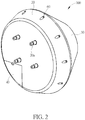
FIGs.2 and3 illustrate the housing of the parabolic antenna inFIG.1 without the alignment bracket. -
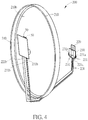
FIG.4 illustrates the parabolic antenna enclosed in the housing ofFIG.1 . -
FIG.5 illustrates a flowchart of a method for determining distance and measurements of the parabolic antenna according to an embodiment of the present invention. -
FIG.6 illustrates a diagram of the parabolic antenna ofFIG.4 for calculating the focal length of the parabolic dish. -
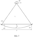
FIG.7 illustrates a diagram of the parabolic antenna ofFIG.4 for calculating the depth of the parabolic dish. -
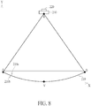
FIG.8 illustrates a diagram of the parabolic antenna ofFIG.4 for calculating the depth of the parabolic dish. -
FIG.1 illustrates ahousing 100 of a parabolic antenna according to an embodiment of the present invention. Thehousing 100 of the parabolic antenna shown inFIG.1 comprises aradome 10, abacking 20 and analignment bracket 30. Theradome 10 may be a plastic radome and is a structural, weatherproof enclosure used to protect the parabolic antenna from the influence of outside environment. Theradome 10 may be constructed using material that minimally attenuates signal transmitted or received by the parabolic antenna. Thebacking 20 may be coupled to theradome 10 usingscrews 60 for example. Thebacking 20 may further comprisescrews 20a to couple thealignment bracket 30 to the parabolic antenna. Thebacking 20 may be a die cast backing. - The
alignment bracket 30 comprises afirst fixing mount 30a, anarm 30b, a first rotatingjoint 30c, a second rotatingjoint 30d, and asecond fixing mount 30e. Thefirst fixing mount 30a is used to mount the parabolic antenna to an external fixed structure using, for example,U-bolts 101. According to alternative embodiments, the parabolic antenna may be supported by any of a wide variety of known mounting apparatus and methods in conjunction with, or in place of, thefirst fixing mount 30a shown inFIG.1 . Thefirst fixing mount 30a may in turn be mounted to other structures such as a radio tower or a building. Thearm 30b is used to couple the first rotatingjoint 30c and the second rotatingjoint 30d to each other. Thealignment bracket 30 may be coupled to thebacking 20 by using thescrews 20a to set thesecond fixing mount 30e onto thebacking 20. - The first rotating
joint 30c may be a type of bearing that couples thefirst fixing mount 30a to thearm 30b and allows thearm 30b to rotate at a range of angles corresponding to thefirst fixing mount 30a. In consequence, the parabolic antenna may be moved along a y-axis according to the rotation of thearm 30b. - The second rotating
joint 30d may be a type of bearing that couples thearm 30b to thesecond fixing mount 30e and allows thesecond fixing mount 30e to rotate at a range of angles corresponding to thearm 30b. In consequence, the parabolic antenna may be moved along an x-axis according to the rotation of thesecond fixing mount 30e. - The first rotating
joint 30c and the second rotatingjoint 30d may be used to adjust the positioning of the parabolic antenna for alignment with respect to a target, for example, another parabolic dish or any type of antenna used to transmit/receive signals. Furthermore, the first rotatingjoint 30c and the second rotatingjoint 30d may have corresponding set screws or other devices to hold the position of the parabolic antenna after positioning. -
FIG.2 and3 illustrate thehousing 100 of the parabolic antenna inFIG.1 without the alignment bracket. As shown inFIG.2 , acover 40 may be coupled to thebacking 20. Thecover 40 may be used to protectconnection ports 50 shown inFIG. 3 from the outside environment when not in use. Theconnection ports 50 may be a part of a processor or acontroller 240 used to transmit or receive signal from an external electronic device. The processor or the controller may be used control or process signals received or transmitted by the parabolic antenna. The processor may also be used to determine the frequency of the signal received or transmitted by the parabolic antenna. -
FIG.4 illustrates theparabolic antenna 200 enclosed in the housing ofFIG.1 . Theparabolic antenna 200 comprises aparabolic dish 210, a firstradiating element 220, and a secondradiating element 230. The firstradiating element 220 and the second radiatingelement 230 may be antennas operating using microwave frequencies having frequency range of 0.3GHz to 300GHz. The firstradiating element 220 may be an antenna operating at higher frequency than the second radiatingelement 230 at a frequency range of 23GHz to 90GHz. As an example, the firstradiating element 220 may be a 60GHZ antenna. AUSB cable 221 may be coupled to the first radiatingelement 220 to be able to digitally interface with the firstradiating element 220. The other end of theUSB cable 221 may be coupled to the processor. Thesecond radiating element 230 may be operating at a frequency range of 2GHz to 8GHz. As an example, thesecond radiating element 230 may be a 5GHz antenna.Coaxial cables 231 may be coupled to thesecond radiating element 230 to transfer signal to and from thesecond radiating element 230. Anend 231a of acoaxial cable 231 may be coupled to one side of at least two sides of thesecond radiating element 230. And anend 231a of anothercoaxial cable 231 may be coupled to another side of at least two sides of thesecond radiating element 230. Anotherend 231b of thecoaxial cables 231 may each be coupled to the processor. - The
parabolic dish 210 has aconvex side 210b and aconcave side 210a. Theconvex side 210b may be the back of theparabolic dish 210 and is covered by the backing 20 of thehousing 100 when enclosed. The processor may be disposed at the back of theparabolic dish 210. Theconcave side 210a may be the front of theparabolic dish 210 and is covered by theradome 10 of thehousing 100 when enclosed. - The
first radiating element 220 and thesecond radiating element 230 may be disposed directly at the focal point of the parabolic antenna. The radiatingelements elements elements elements first radiating element 220 and thesecond radiating element 230 may be positioned such that the opposing edges having first length of thefirst radiating element 220 are in parallel with the opposing edges having second length of the second radiating element 230.Thesecond radiating element 230 may be disposed closer to theparabolic dish 210 relative to thefirst radiating element 220. Thefirst radiating element 220 and thesecond radiating element 230 may or may not be of the same size. - The distance between the radiating
elements parabolic dish 210 may be far enough such that the radiatingelements elements parabolic dish 210. The distance between the radiatingelements parabolic dish 210 may be far enough such that radio frequency (RF) waves received by theparabolic dish 210 may be focused towards the radiatingelements elements parabolic dish 210 is the focal length of theparabolic dish 210. Thefirst radiating element 220 is an antenna having a corresponding antenna chipset. The antenna chipset may be a 60GHz chipset and theconnection ports 50 may be connection ports of the processor to control the radiatingelements parabolic antenna 200. - Furthermore, since the radiating
elements parabolic dish 210, the parabolic antenna of the present invention does not need additional waveguides or directors. Thus, the cost of manufacturing the parabolic antenna is reduced. The radiatingelements parabolic dish 210 using a support or by disposing the radiatingelements radome 10 inFIG.1 . - During the operation of the parabolic antenna, the first radiating element may have a gain amplified according to the requirement of the final application. The processor may be used to determine the signal strength of the first and second radiating elements. The first radiating element and the second radiating element may operate simultaneously or non-simultaneously. During bad weather, the signal of the first radiating element may be affected and may result in worsened transmission/reception. To avoid disturbance in transmission signals, the second radiating element operating at a different frequency may be used as a backup link. The processor may be used to control the switching of operation or simultaneous operation of the first radiating element and the second radiating element. The first radiating element and the second radiating element may share the same parabolic dish. The parabolic antenna may further comprise of an interface to control both the first radiating element and the second radiating element. Thereby, a simple and stable system for the parabolic antenna may be created.
- In an embodiment, the processor may be used to determine the integrity of the signal of the first radiating element. The integrity of the signal may comprise signal strength, signal to noise ratio, and delay of the signal. The integrity of the signal may be affected by outside environment of the parabolic antenna. The signal strength of the signal of the first radiating element may be compared to a predetermined threshold. When the signal strength of the first radiating element is less than the predetermined threshold, the operation of the first radiating element is switched to the second radiating element. In some other embodiments, delay in the transmission or reception of the signal of the first radiating element may be used to determine the switching of operation between the first radiating element and the second radiating element. The switching of operation between the first radiating element and the second radiating element may not cause any delay in the transmission or reception of the signal.
-
FIG.5 illustrates a flowchart of for a method for determining distance and measurements of the parabolic antenna according to an embodiment of the present invention. The method for determining distance and measurements of the parabolic antenna may include, but is not limited to, the following steps:step 301: calculate a focal length of the parabolic dish; step 302: calculate a depth of the parabolic dish according to the focal length; and step 303: calculate a curvature of the parabolic dish according to the focal length. - In
step 301, the focal length of the parabolic dish may be calculated. The focal length is the distance between the vertex of the parabolic dish and the radiating elements.FIG.6 illustrates a diagram of the parabolic antenna ofFIG.4 for calculating the focal length of the parabolic dish. The focal length may be calculated according to the following equation:
- L is the focal length of the parabolic dish;
- D is the diameter of the parabolic dish; and
- Θ is the angle of the radiation pattern of the radiating elements.
- In
step 302, the depth of the parabolic dish may be calculated according to the focal length. The depth may be the height between the edge of the parabolic dish and the deepest point of the parabolic dish.FIG.7 illustrates a diagram of the parabolic antenna ofFIG.4 for calculating the depth of the parabolic dish. The depth may be calculated according to the following equation:
- H is the depth of the parabolic dish;
- L is the focal length of the parabolic dish; The focal length L of the parabolic dish may be the distance between the focal point of the parabolic dish and the deepest point of the concave side of the parabolic dish; and
- D is the diameter of the parabolic dish.
- In
step 303, the curvature of the parabolic dish may be calculated according to the focal length. The curvature may be defined as the amount by which parabolic dish deviates from being flat.FIG.8 illustrates a diagram of the parabolic antenna ofFIG.4 for calculating the depth of the parabolic dish. The curvature of the parabolic dish may be calculated according to the following equation:
- C is the curvature of the parabolic dish;
- Vx is the x-coordinate of the vertex of the parabolic dish;
- Vy is the y-coordinate of the vertex of the parabolic dish; and
- a is the sum of the distance from a vertex of the parabolic dish to the focal point of the parabolic dish and the distance from the vertex to the directrix of the parabolic dish.
- The vertex V may be defined as the deepest point of the concave side of the parabolic dish. The vertex V may have a corresponding x-coordinate Vx and y-coordinate Vy. The x-coordinate may be coordinates in a first direction and the y-coordinates may be coordinates in a second direction. As shown in
FIG.8 , the first direction may be a horizontal direction that is going across the parabolic dish. More particularly, the first direction goes from a first edge point A of the parabolic dish to a second edge point B of the parabolic dish directly across the first edge point A. As shown inFIG.8 , the second direction may be a vertical direction that is going from the deepest part of the parabolic dish towards the radiating elements. More particularly, the second direction goes from the vertex V of the parabolic dish to the surface of radiating antenna directly across the vertex V. - The sum of the distance from the vertex to the focal point and the distance from the vertex to the directrix may be calculated using the following equation:

- a is the sum of the distance from the vertex to the focal point and the distance from the vertex to the directrix;
- Vx is the x-coordinate of the vertex of the parabolic dish;
- Vy is the y-coordinate of the vertex of the parabolic dish;
- Fx is the x-coordinate of the focal point of the parabolic dish; and
- Fy is the y-coordinate of the focal point of the parabolic dish.
- The vertex V may be defined as the deepest point of the concave side of the parabolic dish. The vertex V may have a corresponding x-coordinate Vx and y-coordinate Vy.
- According to an embodiment of the present invention, a parabolic antenna may comprise a radiating element and a parabolic dish. The radiating element may be an antenna of an antenna chipset that is commercially available. The antenna chipset may use a Universal Serial Bus (USB) to connect to other electronic devices. The antenna chipset may have operating frequency of 23GHz to 90GHz and may have operating range of 25 meters. To increase the operating range of the antenna chipset, the parabolic dish as shown in
FIG.4 may be used to amplify the gain of the radiating element of the antenna chipset. The operating range of the antenna chipset may be increased to, for example, 2 kilometers. The increase in the operating range may correspond to the diameter or the focal length of the parabolic dish. The radiating element may be disposed on the concave side of the parabolic dish at a distance equal to the focal length of the parabolic dish. The antenna chipset may be able to process the signal received or transmitted by the radiating element, thus, the parabolic antenna may not have a processor for processing signals. The antenna chipset may be directly coupled to an external electronic device using a USB cable. Furthermore, since the radiating element is placed in front of the parabolic dish, the parabolic antenna of the present invention does not need additional waveguides or directors. - The present invention presents an embodiment of a parabolic antenna having no waveguide or directors to reduce manufacturing cost. The parabolic antenna may comprise radiating elements operating under different frequency disposed at the focal point of the parabolic dish in front of the parabolic dish. The parabolic dish may be shared by the radiating elements. The radiating elements may operate under different conditions including working simultaneously during different data transmission or reception, working simultaneously during same data transmission or reception, and working non-simultaneously during data transmission or reception. Under bad weather conditions, the radiating element having higher operating frequency may be affected causing a decrease in the quality of the transmission link. Thus, use of the radiating element having higher operating frequency may be switched to the use another radiating element having lower operating frequency. For example, the radiating element having higher operating frequency may be a 60GHz antenna and the other radiating element having lower operating frequency may be a 5GHz antenna. The switching of the operation of the radiating elements may be done automatically using a processor or controlled by a user using an interface.
- A further embodiment of a parabolic antenna may comprise a radiating element and a parabolic dish. The radiating element may be a part of an antenna chipset having a USB connector to connect to another electronic device. The antenna chipset may be used to process signals received and transmitted from the radiating element. The parabolic antenna may further comprise a housing to protect the parabolic antenna from outside environment. The radiating element may be disposed at the focal point of the concave side of the parabolic dish. Thus, there is no need for additional waveguides or directors.
Claims (12)
- A parabolic antenna (200), comprising:a parabolic dish (210) having a concave side (210a), and a focal point;a first radiating element (220) disposed above the concave side (210a) of the parabolic dish (210) at the focal point of the parabolic dish (210);a second radiating element (230) disposed at the focal point of the parabolic dish (210);a housing (100) configured to enclose the parabolic dish (210), the first radiating element (220), and the second radiating element (230), the housing comprising:a radome (10); anda backing (20) coupled to the radome (10);and characterized by:a USB cable (221) coupling the first radiating element (220) to a processor (240) to digitally interface with the first radiating element (220);two coaxial cables (231) coupling the second radiating element (230) to the processor (240) to transfer signal to and from the second radiating element (230); andan alignment bracket (30) coupled to the backing (20), the alignment bracket comprising:a first fixing mount (30a) configured to mount the parabolic antenna (200) to a fixed structure;a first rotating joint (30c) coupled to the first fixing mount (30a) and configured to rotate the parabolic antenna (200) along a first direction;an arm (30b) coupled to the first rotating joint (30c);a second rotating joint (30d) coupled to the arm (30b) and configured to rotate the parabolic antenna (200) along another direction; anda second fixing mount (30e) coupled to the second rotating joint (30d) and configured to mount the parabolic antenna (200) onto the alignment bracket (30);wherein the concave side (210a) of the parabolic dish (210) has a focal length, a depth and a curvature; the focal length being a distance between a vertex of the parabolic dish (210) and the first radiating element and the second radiating element; the depth being a height between an edge of the parabolic dish (210) and a deepest point of the parabolic dish (210); the curvature being an amount by which the parabolic dish (210) deviates from being flat.
- The parabolic antenna (200) of claim 1 further characterized in that the focal length is calculated according to following equation:
 L is the focal length of the parabolic dish (210);D is a diameter of the parabolic dish (210); andθ is an angle of the radiation pattern of the radiating elements (220, 230).
 - The parabolic antenna (100, 200) of claim 1 further characterized in that the depth is calculated according to following equation:
 H is the depth of the parabolic dish (210);L is the focal length of the parabolic dish (210); andD is the diameter of the parabolic dish (210).
 - The parabolic antenna (200) of claim 1 further characterized in that the curvature is calculated according to the following equation:
 C is the curvature of the parabolic dish (210);Vx is an x-coordinate of the vertex of the parabolic dish (210);Vy is a y-coordinate of the vertex of the parabolic dish (210); anda is a sum of a distance from a vertex of the parabolic dish (210) to the focal point and a distance from the vertex to a directrix of the parabolic dish (210).
 - The parabolic antenna (200) of claim 1 further characterized in that the sum of the distance from the vertex to the focal point and the distance from the vertex to the directrix is calculated according to the following equation:
 a is the sum of the distance from the vertex to the focal point and the distance from the vertex to the directrix;Vx is the x-coordinate of the vertex of the parabolic dish (210);Vy is the y-coordinate of the vertex of the parabolic dish (210);Fx is an x-coordinate of the focal point of the parabolic dish (210); andFy is a y-coordinate of the focal point of the parabolic dish (210).
 - The parabolic antenna (200) of claim 1, further characterized in that the processor (240) switches operation of the parabolic antenna (200) from the first radiating element (220) to the second radiating element (230) when a signal strength of the signal of the first radiating element (220) is less than a predetermined threshold.
- The parabolic antenna (200) of claim 1, further characterized in that the processor (240) switches operation of the parabolic antenna (200) from the first radiating element (220) to the second radiating element (230) when the signal of the first radiating element (220) experiences a delay.
- The parabolic antenna (200) of claim 1, further characterized in that the antenna chipset is configured to process transmitted or received signals from the first radiating element (220).
- The parabolic antenna (200) of claim 1, further characterized in that an operating frequency of the first radiating element (220) is greater than an operating frequency of the second radiating element (230).
- The parabolic antenna (200) of claim 1, further characterized in that the first radiating element (220) and the second radiating element (230) are positioned to be in perpendicular interlace to each other.
- The parabolic antenna (200) of claim 1, further characterized in that the first radiating element (220) and the second radiating element (230) work simultaneously.
- The parabolic antenna (200) of claim 1, further characterized in that the first radiating element (220) and the second radiating element (230) uniformly radiate radio frequency (RF) waves to the parabolic dish (210).
Priority Applications (1)
| Application Number | Priority Date | Filing Date | Title |
|---|---|---|---|
| PL17180181T PL3249748T3 (en) | 2015-04-02 | 2015-11-04 | Structure of a parabolic antenna |
Applications Claiming Priority (3)
| Application Number | Priority Date | Filing Date | Title |
|---|---|---|---|
| US201562141874P | 2015-04-02 | 2015-04-02 | |
| US14/753,027 US9627773B2 (en) | 2015-04-02 | 2015-06-29 | Structure of a parabolic antenna |
| EP15193034.4A EP3086410B1 (en) | 2015-04-02 | 2015-11-04 | Structure of a parabolic antenna |
Related Parent Applications (2)
| Application Number | Title | Priority Date | Filing Date |
|---|---|---|---|
| EP15193034.4A Division EP3086410B1 (en) | 2015-04-02 | 2015-11-04 | Structure of a parabolic antenna |
| EP15193034.4A Division-Into EP3086410B1 (en) | 2015-04-02 | 2015-11-04 | Structure of a parabolic antenna |
Publications (2)
| Publication Number | Publication Date |
|---|---|
| EP3249748A1 EP3249748A1 (en) | 2017-11-29 |
| EP3249748B1 true EP3249748B1 (en) | 2020-10-14 |
Family
ID=54366147
Family Applications (2)
| Application Number | Title | Priority Date | Filing Date |
|---|---|---|---|
| EP17180181.4A Active EP3249748B1 (en) | 2015-04-02 | 2015-11-04 | Structure of a parabolic antenna |
| EP15193034.4A Not-in-force EP3086410B1 (en) | 2015-04-02 | 2015-11-04 | Structure of a parabolic antenna |
Family Applications After (1)
| Application Number | Title | Priority Date | Filing Date |
|---|---|---|---|
| EP15193034.4A Not-in-force EP3086410B1 (en) | 2015-04-02 | 2015-11-04 | Structure of a parabolic antenna |
Country Status (7)
| Country | Link |
|---|---|
| US (1) | US9627773B2 (en) |
| EP (2) | EP3249748B1 (en) |
| CN (1) | CN106058488B (en) |
| ES (2) | ES2834974T3 (en) |
| HU (2) | HUE052320T2 (en) |
| LT (2) | LT3086410T (en) |
| PL (2) | PL3086410T3 (en) |
Families Citing this family (3)
| Publication number | Priority date | Publication date | Assignee | Title |
|---|---|---|---|---|
| CN107093789A (en) * | 2017-04-24 | 2017-08-25 | 昆山市山山塑胶科技有限公司 | The guidance antenna of high intensity high-low temperature resistant |
| CN107331960B (en) * | 2017-06-26 | 2021-01-01 | 北京无线电测量研究所 | Antenna housing for reflector antenna and manufacturing method thereof |
| CN114784498B (en) * | 2022-05-09 | 2026-03-20 | 深圳市飞翼创新有限公司 | Fine-tuning high-efficiency antennas that can prevent injury from falling debris in severe weather and their prevention methods |
Family Cites Families (22)
| Publication number | Priority date | Publication date | Assignee | Title |
|---|---|---|---|---|
| US4090203A (en) | 1975-09-29 | 1978-05-16 | Trw Inc. | Low sidelobe antenna system employing plural spaced feeds with amplitude control |
| US4864317A (en) | 1983-02-07 | 1989-09-05 | Sorko Ram Paul O | Combination satellite antenna-solar collector |
| JPH0936655A (en) * | 1995-07-18 | 1997-02-07 | Nippon Antenna Co Ltd | Multi-beam antenna |
| US5815125A (en) * | 1997-02-05 | 1998-09-29 | W. L. Gore & Associates, Inc. | Satellite dish cover |
| CA2204295C (en) * | 1997-05-02 | 2001-09-11 | Francis Edward Bowman | Satellite receiving dish feed horn or lnb cover |
| DE19845868A1 (en) * | 1998-10-05 | 2000-04-06 | Pates Tech Patentverwertung | Dual focus planar antenna |
| TW395066B (en) * | 1998-10-09 | 2000-06-21 | Acer Inc | Satellite dish antenna microstrip array feed device |
| US6512492B2 (en) * | 2001-02-06 | 2003-01-28 | Harris Broadband Wireless Access, Inc. | Antenna quick connect system and method |
| CN2508471Y (en) * | 2001-09-27 | 2002-08-28 | 曹胜旭 | Single offset feedforward parabolic antenna |
| US6714167B1 (en) * | 2002-08-19 | 2004-03-30 | Raymond M. Gusick, Jr. | Satellite dish cover |
| DE60308409T2 (en) * | 2002-10-24 | 2007-09-20 | Centre National De La Recherche Scientifique (C.N.R.S.) | MULTI-STREAM LENS WITH PHOTONIC BELT MATERIAL |
| US6879298B1 (en) | 2003-10-15 | 2005-04-12 | Harris Corporation | Multi-band horn antenna using corrugations having frequency selective surfaces |
| AU2003304695A1 (en) | 2003-12-31 | 2005-08-12 | Brunello Locatori | Method and device for tv receiving and internet transreceiving on a satellite antenna |
| US7187334B2 (en) * | 2004-10-29 | 2007-03-06 | Motorola, Inc. | Patch array feed for an automotive radar antenna |
| US7215300B1 (en) * | 2004-11-01 | 2007-05-08 | Dish Rags, Inc. | Satellite dish cover |
| US7277064B2 (en) * | 2005-09-29 | 2007-10-02 | Hogsett Samuel W | Satellite dish facade with magnet |
| US7576701B2 (en) | 2007-04-02 | 2009-08-18 | Raytheon Company | Rotating screen dual reflector antenna |
| US8552918B2 (en) * | 2009-01-02 | 2013-10-08 | Laird Technologies, Inc. | Multiband high gain omnidirectional antennas |
| US9231142B2 (en) * | 2009-10-06 | 2016-01-05 | Brightleaf Technologies Inc. | Non-parabolic solar concentration to an area of controlled flux density conversion system and method |
| CN201985251U (en) * | 2011-01-06 | 2011-09-21 | 广东盛华德通讯科技股份有限公司 | Broadband parabolic antenna |
| US20120176608A1 (en) * | 2011-01-07 | 2012-07-12 | Mccown James Charles | System and method for antenna alignment |
| EP2843761B1 (en) * | 2013-08-30 | 2018-07-04 | Alcatel- Lucent Shanghai Bell Co., Ltd | Compact antenna system |
-
2015
- 2015-06-29 US US14/753,027 patent/US9627773B2/en active Active
- 2015-08-04 CN CN201510469203.XA patent/CN106058488B/en active Active
- 2015-11-04 HU HUE15193034A patent/HUE052320T2/en unknown
- 2015-11-04 HU HUE17180181A patent/HUE052949T2/en unknown
- 2015-11-04 ES ES17180181T patent/ES2834974T3/en active Active
- 2015-11-04 EP EP17180181.4A patent/EP3249748B1/en active Active
- 2015-11-04 LT LTEP15193034.4T patent/LT3086410T/en unknown
- 2015-11-04 PL PL15193034T patent/PL3086410T3/en unknown
- 2015-11-04 EP EP15193034.4A patent/EP3086410B1/en not_active Not-in-force
- 2015-11-04 LT LTEP17180181.4T patent/LT3249748T/en unknown
- 2015-11-04 PL PL17180181T patent/PL3249748T3/en unknown
- 2015-11-04 ES ES15193034T patent/ES2834639T3/en active Active
Non-Patent Citations (1)
| Title |
|---|
| None * |
Also Published As
| Publication number | Publication date |
|---|---|
| ES2834974T3 (en) | 2021-06-21 |
| US20160294069A1 (en) | 2016-10-06 |
| LT3086410T (en) | 2020-11-25 |
| CN106058488A (en) | 2016-10-26 |
| EP3086410A3 (en) | 2017-01-11 |
| US9627773B2 (en) | 2017-04-18 |
| HUE052320T2 (en) | 2021-04-28 |
| CN106058488B (en) | 2019-05-21 |
| HUE052949T2 (en) | 2021-05-28 |
| EP3249748A1 (en) | 2017-11-29 |
| LT3249748T (en) | 2020-11-25 |
| EP3086410B1 (en) | 2020-10-14 |
| ES2834639T3 (en) | 2021-06-18 |
| PL3249748T3 (en) | 2021-05-17 |
| EP3086410A2 (en) | 2016-10-26 |
| PL3086410T3 (en) | 2021-05-17 |
Similar Documents
| Publication | Publication Date | Title |
|---|---|---|
| US11069979B2 (en) | Vertically polarized omnidirectional antenna and dual-polarization omnidirectional antenna thereof | |
| WO2019150666A1 (en) | Antenna module and vehicle | |
| WO2016029631A1 (en) | Antenna and communication device | |
| US10312584B2 (en) | Dual antenna device | |
| US9793973B2 (en) | Non-feeding reradiating repeater and method for manufacturing of the same | |
| JP2015159354A (en) | Collective antenna device | |
| JP7033551B2 (en) | Device for antenna alignment | |
| EP3086410B1 (en) | Structure of a parabolic antenna | |
| US7498995B2 (en) | UWB antenna having 270 degree coverage and system thereof | |
| CN105789820A (en) | Antenna structure and wireless communication device with same | |
| US9419338B2 (en) | Antenna apparatus | |
| KR101880707B1 (en) | System for controlling direction of directional antenna and method for controlling direction thereof | |
| EP2467899B1 (en) | Directional planar log-spiral slot antenna | |
| KR20180047392A (en) | Antenna apparatus | |
| CN112768888A (en) | Antenna array element and array antenna | |
| CN101740868B (en) | Single-polarization antenna | |
| WO2013153784A1 (en) | Antenna device | |
| CN209804892U (en) | Microstrip antenna loaded with parasitic patch | |
| US4737796A (en) | Ground plane interference elimination by passive element | |
| US9397394B2 (en) | Antenna arrays with modified Yagi antenna units | |
| KR102053914B1 (en) | Interior test apparatus for performance of wireless telecommunication system | |
| US20200014096A1 (en) | Antenna Waveguide and Antenna Module Thereof | |
| CN105390818A (en) | Radiation device | |
| JP2016111505A (en) | Vehicle glass antenna and vehicle window glass | |
| KR100849703B1 (en) | Parallel Feeding Low Angle High Gain Circularly Polarized Antenna |
Legal Events
| Date | Code | Title | Description |
|---|---|---|---|
| PUAI | Public reference made under article 153(3) epc to a published international application that has entered the european phase |
Free format text: ORIGINAL CODE: 0009012 |
|
| STAA | Information on the status of an ep patent application or granted ep patent |
Free format text: STATUS: THE APPLICATION HAS BEEN PUBLISHED |
|
| AC | Divisional application: reference to earlier application |
Ref document number: 3086410 Country of ref document: EP Kind code of ref document: P |
|
| AK | Designated contracting states |
Kind code of ref document: A1 Designated state(s): AL AT BE BG CH CY CZ DE DK EE ES FI FR GB GR HR HU IE IS IT LI LT LU LV MC MK MT NL NO PL PT RO RS SE SI SK SM TR |
|
| AX | Request for extension of the european patent |
Extension state: BA ME |
|
| STAA | Information on the status of an ep patent application or granted ep patent |
Free format text: STATUS: REQUEST FOR EXAMINATION WAS MADE |
|
| 17P | Request for examination filed |
Effective date: 20180516 |
|
| RBV | Designated contracting states (corrected) |
Designated state(s): AL AT BE BG CH CY CZ DE DK EE ES FI FR GB GR HR HU IE IS IT LI LT LU LV MC MK MT NL NO PL PT RO RS SE SI SK SM TR |
|
| GRAP | Despatch of communication of intention to grant a patent |
Free format text: ORIGINAL CODE: EPIDOSNIGR1 |
|
| STAA | Information on the status of an ep patent application or granted ep patent |
Free format text: STATUS: GRANT OF PATENT IS INTENDED |
|
| INTG | Intention to grant announced |
Effective date: 20200511 |
|
| RIN1 | Information on inventor provided before grant (corrected) |
Inventor name: DEWEY, CHAD ELLIOT Inventor name: BLEDSOE, HAROLD RIBER |
|
| GRAS | Grant fee paid |
Free format text: ORIGINAL CODE: EPIDOSNIGR3 |
|
| GRAA | (expected) grant |
Free format text: ORIGINAL CODE: 0009210 |
|
| STAA | Information on the status of an ep patent application or granted ep patent |
Free format text: STATUS: THE PATENT HAS BEEN GRANTED |
|
| AC | Divisional application: reference to earlier application |
Ref document number: 3086410 Country of ref document: EP Kind code of ref document: P |
|
| AK | Designated contracting states |
Kind code of ref document: B1 Designated state(s): AL AT BE BG CH CY CZ DE DK EE ES FI FR GB GR HR HU IE IS IT LI LT LU LV MC MK MT NL NO PL PT RO RS SE SI SK SM TR |
|
| REG | Reference to a national code |
Ref country code: GB Ref legal event code: FG4D |
|
| REG | Reference to a national code |
Ref country code: AT Ref legal event code: REF Ref document number: 1324490 Country of ref document: AT Kind code of ref document: T Effective date: 20201015 Ref country code: CH Ref legal event code: EP |
|
| REG | Reference to a national code |
Ref country code: DE Ref legal event code: R096 Ref document number: 602015060653 Country of ref document: DE |
|
| REG | Reference to a national code |
Ref country code: IE Ref legal event code: FG4D |
|
| REG | Reference to a national code |
Ref country code: NL Ref legal event code: FP |
|
| REG | Reference to a national code |
Ref country code: AT Ref legal event code: MK05 Ref document number: 1324490 Country of ref document: AT Kind code of ref document: T Effective date: 20201014 |
|
| PG25 | Lapsed in a contracting state [announced via postgrant information from national office to epo] |
Ref country code: FI Free format text: LAPSE BECAUSE OF FAILURE TO SUBMIT A TRANSLATION OF THE DESCRIPTION OR TO PAY THE FEE WITHIN THE PRESCRIBED TIME-LIMIT Effective date: 20201014 Ref country code: RS Free format text: LAPSE BECAUSE OF FAILURE TO SUBMIT A TRANSLATION OF THE DESCRIPTION OR TO PAY THE FEE WITHIN THE PRESCRIBED TIME-LIMIT Effective date: 20201014 Ref country code: PT Free format text: LAPSE BECAUSE OF FAILURE TO SUBMIT A TRANSLATION OF THE DESCRIPTION OR TO PAY THE FEE WITHIN THE PRESCRIBED TIME-LIMIT Effective date: 20210215 Ref country code: NO Free format text: LAPSE BECAUSE OF FAILURE TO SUBMIT A TRANSLATION OF THE DESCRIPTION OR TO PAY THE FEE WITHIN THE PRESCRIBED TIME-LIMIT Effective date: 20210114 |
|
| REG | Reference to a national code |
Ref country code: HU Ref legal event code: AG4A Ref document number: E052949 Country of ref document: HU |
|
| PG25 | Lapsed in a contracting state [announced via postgrant information from national office to epo] |
Ref country code: SE Free format text: LAPSE BECAUSE OF FAILURE TO SUBMIT A TRANSLATION OF THE DESCRIPTION OR TO PAY THE FEE WITHIN THE PRESCRIBED TIME-LIMIT Effective date: 20201014 Ref country code: IS Free format text: LAPSE BECAUSE OF FAILURE TO SUBMIT A TRANSLATION OF THE DESCRIPTION OR TO PAY THE FEE WITHIN THE PRESCRIBED TIME-LIMIT Effective date: 20210214 Ref country code: BG Free format text: LAPSE BECAUSE OF FAILURE TO SUBMIT A TRANSLATION OF THE DESCRIPTION OR TO PAY THE FEE WITHIN THE PRESCRIBED TIME-LIMIT Effective date: 20210114 Ref country code: AT Free format text: LAPSE BECAUSE OF FAILURE TO SUBMIT A TRANSLATION OF THE DESCRIPTION OR TO PAY THE FEE WITHIN THE PRESCRIBED TIME-LIMIT Effective date: 20201014 |
|
| REG | Reference to a national code |
Ref country code: ES Ref legal event code: FG2A Ref document number: 2834974 Country of ref document: ES Kind code of ref document: T3 Effective date: 20210621 |
|
| PG25 | Lapsed in a contracting state [announced via postgrant information from national office to epo] |
Ref country code: HR Free format text: LAPSE BECAUSE OF FAILURE TO SUBMIT A TRANSLATION OF THE DESCRIPTION OR TO PAY THE FEE WITHIN THE PRESCRIBED TIME-LIMIT Effective date: 20201014 |
|
| REG | Reference to a national code |
Ref country code: CH Ref legal event code: PL |
|
| REG | Reference to a national code |
Ref country code: DE Ref legal event code: R097 Ref document number: 602015060653 Country of ref document: DE |
|
| PG25 | Lapsed in a contracting state [announced via postgrant information from national office to epo] |
Ref country code: SK Free format text: LAPSE BECAUSE OF FAILURE TO SUBMIT A TRANSLATION OF THE DESCRIPTION OR TO PAY THE FEE WITHIN THE PRESCRIBED TIME-LIMIT Effective date: 20201014 Ref country code: RO Free format text: LAPSE BECAUSE OF FAILURE TO SUBMIT A TRANSLATION OF THE DESCRIPTION OR TO PAY THE FEE WITHIN THE PRESCRIBED TIME-LIMIT Effective date: 20201014 Ref country code: EE Free format text: LAPSE BECAUSE OF FAILURE TO SUBMIT A TRANSLATION OF THE DESCRIPTION OR TO PAY THE FEE WITHIN THE PRESCRIBED TIME-LIMIT Effective date: 20201014 Ref country code: SM Free format text: LAPSE BECAUSE OF FAILURE TO SUBMIT A TRANSLATION OF THE DESCRIPTION OR TO PAY THE FEE WITHIN THE PRESCRIBED TIME-LIMIT Effective date: 20201014 Ref country code: MC Free format text: LAPSE BECAUSE OF FAILURE TO SUBMIT A TRANSLATION OF THE DESCRIPTION OR TO PAY THE FEE WITHIN THE PRESCRIBED TIME-LIMIT Effective date: 20201014 Ref country code: LU Free format text: LAPSE BECAUSE OF NON-PAYMENT OF DUE FEES Effective date: 20201104 |
|
| REG | Reference to a national code |
Ref country code: BE Ref legal event code: MM Effective date: 20201130 |
|
| PLBE | No opposition filed within time limit |
Free format text: ORIGINAL CODE: 0009261 |
|
| STAA | Information on the status of an ep patent application or granted ep patent |
Free format text: STATUS: NO OPPOSITION FILED WITHIN TIME LIMIT |
|
| PG25 | Lapsed in a contracting state [announced via postgrant information from national office to epo] |
Ref country code: LI Free format text: LAPSE BECAUSE OF NON-PAYMENT OF DUE FEES Effective date: 20201130 Ref country code: DK Free format text: LAPSE BECAUSE OF FAILURE TO SUBMIT A TRANSLATION OF THE DESCRIPTION OR TO PAY THE FEE WITHIN THE PRESCRIBED TIME-LIMIT Effective date: 20201014 Ref country code: CH Free format text: LAPSE BECAUSE OF NON-PAYMENT OF DUE FEES Effective date: 20201130 |
|
| 26N | No opposition filed |
Effective date: 20210715 |
|
| PG25 | Lapsed in a contracting state [announced via postgrant information from national office to epo] |
Ref country code: IE Free format text: LAPSE BECAUSE OF NON-PAYMENT OF DUE FEES Effective date: 20201104 Ref country code: AL Free format text: LAPSE BECAUSE OF FAILURE TO SUBMIT A TRANSLATION OF THE DESCRIPTION OR TO PAY THE FEE WITHIN THE PRESCRIBED TIME-LIMIT Effective date: 20201014 |
|
| PG25 | Lapsed in a contracting state [announced via postgrant information from national office to epo] |
Ref country code: SI Free format text: LAPSE BECAUSE OF FAILURE TO SUBMIT A TRANSLATION OF THE DESCRIPTION OR TO PAY THE FEE WITHIN THE PRESCRIBED TIME-LIMIT Effective date: 20201014 |
|
| PGFP | Annual fee paid to national office [announced via postgrant information from national office to epo] |
Ref country code: TR Payment date: 20211015 Year of fee payment: 7 Ref country code: NL Payment date: 20211125 Year of fee payment: 7 |
|
| PGFP | Annual fee paid to national office [announced via postgrant information from national office to epo] |
Ref country code: HU Payment date: 20211019 Year of fee payment: 7 Ref country code: GR Payment date: 20211118 Year of fee payment: 7 |
|
| PG25 | Lapsed in a contracting state [announced via postgrant information from national office to epo] |
Ref country code: IS Free format text: LAPSE BECAUSE OF FAILURE TO SUBMIT A TRANSLATION OF THE DESCRIPTION OR TO PAY THE FEE WITHIN THE PRESCRIBED TIME-LIMIT Effective date: 20210214 Ref country code: MT Free format text: LAPSE BECAUSE OF FAILURE TO SUBMIT A TRANSLATION OF THE DESCRIPTION OR TO PAY THE FEE WITHIN THE PRESCRIBED TIME-LIMIT Effective date: 20201014 Ref country code: CY Free format text: LAPSE BECAUSE OF FAILURE TO SUBMIT A TRANSLATION OF THE DESCRIPTION OR TO PAY THE FEE WITHIN THE PRESCRIBED TIME-LIMIT Effective date: 20201014 |
|
| PGFP | Annual fee paid to national office [announced via postgrant information from national office to epo] |
Ref country code: PL Payment date: 20211011 Year of fee payment: 7 |
|
| PG25 | Lapsed in a contracting state [announced via postgrant information from national office to epo] |
Ref country code: MK Free format text: LAPSE BECAUSE OF FAILURE TO SUBMIT A TRANSLATION OF THE DESCRIPTION OR TO PAY THE FEE WITHIN THE PRESCRIBED TIME-LIMIT Effective date: 20201014 |
|
| PG25 | Lapsed in a contracting state [announced via postgrant information from national office to epo] |
Ref country code: BE Free format text: LAPSE BECAUSE OF NON-PAYMENT OF DUE FEES Effective date: 20201130 |
|
| PGFP | Annual fee paid to national office [announced via postgrant information from national office to epo] |
Ref country code: GB Payment date: 20220916 Year of fee payment: 8 |
|
| PGFP | Annual fee paid to national office [announced via postgrant information from national office to epo] |
Ref country code: FR Payment date: 20220916 Year of fee payment: 8 |
|
| PGFP | Annual fee paid to national office [announced via postgrant information from national office to epo] |
Ref country code: IT Payment date: 20221122 Year of fee payment: 8 Ref country code: ES Payment date: 20221202 Year of fee payment: 8 Ref country code: DE Payment date: 20220922 Year of fee payment: 8 Ref country code: CZ Payment date: 20221102 Year of fee payment: 8 Ref country code: LV Payment date: 20221121 Year of fee payment: 8 Ref country code: LT Payment date: 20221014 Year of fee payment: 8 |
|
| REG | Reference to a national code |
Ref country code: NL Ref legal event code: MM Effective date: 20221201 |
|
| PG25 | Lapsed in a contracting state [announced via postgrant information from national office to epo] |
Ref country code: HU Free format text: LAPSE BECAUSE OF NON-PAYMENT OF DUE FEES Effective date: 20221105 |
|
| PG25 | Lapsed in a contracting state [announced via postgrant information from national office to epo] |
Ref country code: NL Free format text: LAPSE BECAUSE OF NON-PAYMENT OF DUE FEES Effective date: 20221201 Ref country code: GR Free format text: LAPSE BECAUSE OF NON-PAYMENT OF DUE FEES Effective date: 20230609 |
|
| PG25 | Lapsed in a contracting state [announced via postgrant information from national office to epo] |
Ref country code: PL Free format text: LAPSE BECAUSE OF NON-PAYMENT OF DUE FEES Effective date: 20221104 |
|
| REG | Reference to a national code |
Ref country code: DE Ref legal event code: R119 Ref document number: 602015060653 Country of ref document: DE |
|
| REG | Reference to a national code |
Ref country code: LT Ref legal event code: MM4D Effective date: 20231104 |
|
| PG25 | Lapsed in a contracting state [announced via postgrant information from national office to epo] |
Ref country code: LT Free format text: LAPSE BECAUSE OF NON-PAYMENT OF DUE FEES Effective date: 20231104 |
|
| PG25 | Lapsed in a contracting state [announced via postgrant information from national office to epo] |
Ref country code: CZ Free format text: LAPSE BECAUSE OF NON-PAYMENT OF DUE FEES Effective date: 20231104 |
|
| GBPC | Gb: european patent ceased through non-payment of renewal fee |
Effective date: 20231104 |
|
| PG25 | Lapsed in a contracting state [announced via postgrant information from national office to epo] |
Ref country code: LT Free format text: LAPSE BECAUSE OF NON-PAYMENT OF DUE FEES Effective date: 20231104 Ref country code: CZ Free format text: LAPSE BECAUSE OF NON-PAYMENT OF DUE FEES Effective date: 20231104 |
|
| PG25 | Lapsed in a contracting state [announced via postgrant information from national office to epo] |
Ref country code: LV Free format text: LAPSE BECAUSE OF NON-PAYMENT OF DUE FEES Effective date: 20231104 |
|
| PG25 | Lapsed in a contracting state [announced via postgrant information from national office to epo] |
Ref country code: DE Free format text: LAPSE BECAUSE OF NON-PAYMENT OF DUE FEES Effective date: 20240601 |
|
| PG25 | Lapsed in a contracting state [announced via postgrant information from national office to epo] |
Ref country code: GB Free format text: LAPSE BECAUSE OF NON-PAYMENT OF DUE FEES Effective date: 20231104 |
|
| PG25 | Lapsed in a contracting state [announced via postgrant information from national office to epo] |
Ref country code: FR Free format text: LAPSE BECAUSE OF NON-PAYMENT OF DUE FEES Effective date: 20231130 |
|
| PG25 | Lapsed in a contracting state [announced via postgrant information from national office to epo] |
Ref country code: GB Free format text: LAPSE BECAUSE OF NON-PAYMENT OF DUE FEES Effective date: 20231104 Ref country code: FR Free format text: LAPSE BECAUSE OF NON-PAYMENT OF DUE FEES Effective date: 20231130 Ref country code: DE Free format text: LAPSE BECAUSE OF NON-PAYMENT OF DUE FEES Effective date: 20240601 |
|
| PG25 | Lapsed in a contracting state [announced via postgrant information from national office to epo] |
Ref country code: IT Free format text: LAPSE BECAUSE OF NON-PAYMENT OF DUE FEES Effective date: 20231104 |
|
| PG25 | Lapsed in a contracting state [announced via postgrant information from national office to epo] |
Ref country code: IT Free format text: LAPSE BECAUSE OF NON-PAYMENT OF DUE FEES Effective date: 20231104 |
|
| REG | Reference to a national code |
Ref country code: ES Ref legal event code: FD2A Effective date: 20250102 |
|
| PG25 | Lapsed in a contracting state [announced via postgrant information from national office to epo] |
Ref country code: ES Free format text: LAPSE BECAUSE OF NON-PAYMENT OF DUE FEES Effective date: 20231105 |
|
| PG25 | Lapsed in a contracting state [announced via postgrant information from national office to epo] |
Ref country code: ES Free format text: LAPSE BECAUSE OF NON-PAYMENT OF DUE FEES Effective date: 20231105 |