EP3249535A1 - Assessing performance of a hardware design using formal verification - Google Patents
Assessing performance of a hardware design using formal verification Download PDFInfo
- Publication number
- EP3249535A1 EP3249535A1 EP17172921.3A EP17172921A EP3249535A1 EP 3249535 A1 EP3249535 A1 EP 3249535A1 EP 17172921 A EP17172921 A EP 17172921A EP 3249535 A1 EP3249535 A1 EP 3249535A1
- Authority
- EP
- European Patent Office
- Prior art keywords
- task
- hardware design
- symbolic
- hardware
- cycles
- Prior art date
- Legal status (The legal status is an assumption and is not a legal conclusion. Google has not performed a legal analysis and makes no representation as to the accuracy of the status listed.)
- Granted
Links
Images


Classifications
-
- G—PHYSICS
- G06—COMPUTING OR CALCULATING; COUNTING
- G06F—ELECTRIC DIGITAL DATA PROCESSING
- G06F11/00—Error detection; Error correction; Monitoring
- G06F11/30—Monitoring
- G06F11/3003—Monitoring arrangements specially adapted to the computing system or computing system component being monitored
- G06F11/3024—Monitoring arrangements specially adapted to the computing system or computing system component being monitored where the computing system component is a central processing unit [CPU]
-
- G—PHYSICS
- G06—COMPUTING OR CALCULATING; COUNTING
- G06F—ELECTRIC DIGITAL DATA PROCESSING
- G06F11/00—Error detection; Error correction; Monitoring
- G06F11/30—Monitoring
- G06F11/34—Recording or statistical evaluation of computer activity, e.g. of down time, of input/output operation ; Recording or statistical evaluation of user activity, e.g. usability assessment
- G06F11/3409—Recording or statistical evaluation of computer activity, e.g. of down time, of input/output operation ; Recording or statistical evaluation of user activity, e.g. usability assessment for performance assessment
-
- G—PHYSICS
- G06—COMPUTING OR CALCULATING; COUNTING
- G06F—ELECTRIC DIGITAL DATA PROCESSING
- G06F11/00—Error detection; Error correction; Monitoring
- G06F11/30—Monitoring
- G06F11/34—Recording or statistical evaluation of computer activity, e.g. of down time, of input/output operation ; Recording or statistical evaluation of user activity, e.g. usability assessment
- G06F11/3409—Recording or statistical evaluation of computer activity, e.g. of down time, of input/output operation ; Recording or statistical evaluation of user activity, e.g. usability assessment for performance assessment
- G06F11/3419—Recording or statistical evaluation of computer activity, e.g. of down time, of input/output operation ; Recording or statistical evaluation of user activity, e.g. usability assessment for performance assessment by assessing time
-
- G—PHYSICS
- G06—COMPUTING OR CALCULATING; COUNTING
- G06F—ELECTRIC DIGITAL DATA PROCESSING
- G06F11/00—Error detection; Error correction; Monitoring
- G06F11/30—Monitoring
- G06F11/34—Recording or statistical evaluation of computer activity, e.g. of down time, of input/output operation ; Recording or statistical evaluation of user activity, e.g. usability assessment
- G06F11/3466—Performance evaluation by tracing or monitoring
-
- G—PHYSICS
- G06—COMPUTING OR CALCULATING; COUNTING
- G06F—ELECTRIC DIGITAL DATA PROCESSING
- G06F11/00—Error detection; Error correction; Monitoring
- G06F11/36—Prevention of errors by analysis, debugging or testing of software
- G06F11/3604—Analysis of software for verifying properties of programs
- G06F11/3608—Analysis of software for verifying properties of programs using formal methods, e.g. model checking, abstract interpretation
-
- G—PHYSICS
- G06—COMPUTING OR CALCULATING; COUNTING
- G06F—ELECTRIC DIGITAL DATA PROCESSING
- G06F11/00—Error detection; Error correction; Monitoring
- G06F11/36—Prevention of errors by analysis, debugging or testing of software
- G06F11/3604—Analysis of software for verifying properties of programs
- G06F11/3616—Analysis of software for verifying properties of programs using software metrics
-
- G—PHYSICS
- G06—COMPUTING OR CALCULATING; COUNTING
- G06F—ELECTRIC DIGITAL DATA PROCESSING
- G06F11/00—Error detection; Error correction; Monitoring
- G06F11/36—Prevention of errors by analysis, debugging or testing of software
- G06F11/362—Debugging of software
- G06F11/3636—Debugging of software by tracing the execution of the program
-
- G—PHYSICS
- G06—COMPUTING OR CALCULATING; COUNTING
- G06F—ELECTRIC DIGITAL DATA PROCESSING
- G06F11/00—Error detection; Error correction; Monitoring
- G06F11/36—Prevention of errors by analysis, debugging or testing of software
- G06F11/362—Debugging of software
- G06F11/3648—Debugging of software using additional hardware
-
- G—PHYSICS
- G06—COMPUTING OR CALCULATING; COUNTING
- G06F—ELECTRIC DIGITAL DATA PROCESSING
- G06F11/00—Error detection; Error correction; Monitoring
- G06F11/36—Prevention of errors by analysis, debugging or testing of software
- G06F11/362—Debugging of software
- G06F11/3648—Debugging of software using additional hardware
- G06F11/3652—Debugging of software using additional hardware in-circuit-emulation [ICE] arrangements
-
- G—PHYSICS
- G06—COMPUTING OR CALCULATING; COUNTING
- G06F—ELECTRIC DIGITAL DATA PROCESSING
- G06F30/00—Computer-aided design [CAD]
-
- G—PHYSICS
- G06—COMPUTING OR CALCULATING; COUNTING
- G06F—ELECTRIC DIGITAL DATA PROCESSING
- G06F30/00—Computer-aided design [CAD]
- G06F30/30—Circuit design
-
- G—PHYSICS
- G06—COMPUTING OR CALCULATING; COUNTING
- G06F—ELECTRIC DIGITAL DATA PROCESSING
- G06F30/00—Computer-aided design [CAD]
- G06F30/30—Circuit design
- G06F30/32—Circuit design at the digital level
- G06F30/33—Design verification, e.g. functional simulation or model checking
- G06F30/3323—Design verification, e.g. functional simulation or model checking using formal methods, e.g. equivalence checking or property checking
-
- G—PHYSICS
- G06—COMPUTING OR CALCULATING; COUNTING
- G06F—ELECTRIC DIGITAL DATA PROCESSING
- G06F30/00—Computer-aided design [CAD]
- G06F30/30—Circuit design
- G06F30/39—Circuit design at the physical level
-
- G—PHYSICS
- G06—COMPUTING OR CALCULATING; COUNTING
- G06F—ELECTRIC DIGITAL DATA PROCESSING
- G06F30/00—Computer-aided design [CAD]
- G06F30/30—Circuit design
- G06F30/39—Circuit design at the physical level
- G06F30/398—Design verification or optimisation, e.g. using design rule check [DRC], layout versus schematics [LVS] or finite element methods [FEM]
-
- G—PHYSICS
- G06—COMPUTING OR CALCULATING; COUNTING
- G06F—ELECTRIC DIGITAL DATA PROCESSING
- G06F2119/00—Details relating to the type or aim of the analysis or the optimisation
- G06F2119/18—Manufacturability analysis or optimisation for manufacturability
-
- Y—GENERAL TAGGING OF NEW TECHNOLOGICAL DEVELOPMENTS; GENERAL TAGGING OF CROSS-SECTIONAL TECHNOLOGIES SPANNING OVER SEVERAL SECTIONS OF THE IPC; TECHNICAL SUBJECTS COVERED BY FORMER USPC CROSS-REFERENCE ART COLLECTIONS [XRACs] AND DIGESTS
- Y02—TECHNOLOGIES OR APPLICATIONS FOR MITIGATION OR ADAPTATION AGAINST CLIMATE CHANGE
- Y02P—CLIMATE CHANGE MITIGATION TECHNOLOGIES IN THE PRODUCTION OR PROCESSING OF GOODS
- Y02P90/00—Enabling technologies with a potential contribution to greenhouse gas [GHG] emissions mitigation
- Y02P90/02—Total factory control, e.g. smart factories, flexible manufacturing systems [FMS] or integrated manufacturing systems [IMS]
Definitions
- an electronic system e.g. a processor
- a component thereof is often designed to have a small area footprint and satisfy a low power requirement
- desired performance goals e.g. performs one or more desired tasks within a certain time limit.
- the electronic system is a processor it may be desirable that the processor executes instructions within a certain time limit.
- the hardware monitors include monitoring and counting logic configured to count a number of cycles between start and completion of a symbolic task in the hardware design; and property evaluation logic configured to evaluate one or more formal properties related to the counted number of cycles to assess the performance of the hardware design in completing the symbolic task.
- the hardware monitors may be used by a formal verification tool to exhaustively verify that the hardware design meets a desired performance goal and/or to exhaustively identify a performance metric (e.g. best case and/or worst case performance) with respect to completion of the task.
- a first aspect provides a hardware monitor arranged to assess performance of a hardware design for an integrated circuit to complete a task, the hardware monitor comprising: monitoring and counting logic configured to count a number of cycles between start and completion of the symbolic task in the hardware design; and property evaluation logic configured to evaluate one or more formal properties related to the counted number of cycles to assess the performance of the hardware design in completing the symbolic task.
- a second aspect provides a method of assessing the performance of a hardware design for an integrated circuit to complete a task, the method comprising: receiving the hardware design and a hardware monitor according to the first aspect; formally verifying, using a formal verification tool, the one or more formal properties hold for the hardware design; and outputting an indication of whether or not each of the one or more formal properties was successfully verified, the indication providing an exhaustive assessment of the performance of the hardware design in completing the task.
- a third aspect provides a system configured to assess performance of a hardware design for an integrated circuit to complete a task, the system comprising: a memory configured to store: the hardware design; a formal verification tool; and the hardware monitor of any of the first aspect; one or more processors configured to: formally verify, using the formal verification tool, that the one or more formal properties hold for the hardware design; and output an indication of whether or not each of the one or more formal properties was successfully verified, the indication providing an exhaustive assessment of the performance of the hardware design in completing the task.
- Embodiments described herein relate to methods, hardware monitors, and systems for assessing the performance of a hardware design to complete a task using formal verification (which may be referred to herein simply as "formal"). Assessing the performance of a hardware design to complete a task may comprise verifying that that the hardware design meets a performance goal in completing the task and/or identifying a performance metric for completing the task.
- performance goal is used herein to mean a quantified objective related to completion of the task and includes, but is not limited to, completion of the task within a predetermined number of clock cycles, and, completion of the task by within a predetermined range of clock cycles.
- performance metric is used herein to mean a measureable criterion related to completing the task, and includes, but is not limited to, the worst case (or highest) number of clock cycles to complete the task, and, the best case (or lowest) number of clock cycles to complete the task.
- the hardware monitors described herein are configured to count the number of cycles (e.g. clock cycles) between the start and completion of the task in the hardware design; and evaluate one or more formal properties related to the counted number of cycles to assess the performance of the hardware design in completing the task.
- a formal verification tool can then be used to formally verify that the one or more formal properties holds for all valid states of the hardware design to exhaustively assess the performance of the hardware design in completing the task.
- formal verification the hardware design is transformed into a mathematical model (e.g. a state-transition system) and the properties to be verified are expressed using mathematical logic using a precise syntax or a language with a precise mathematical syntax and semantics. A property is then verified by searching the entire reachable state space of the hardware design without explicitly traversing the state machine. Since formal verification algorithmically and exhaustively explores all input values over time, verifying properties in this manner allows a property to be exhaustively proved or disproved for all valid states. In the embodiments described herein formal verification allows exhaustive assessment of the performance of the hardware design in completing the task. In other words it allows (i) exhaustive verification that the hardware design meets a performance goal with respect to the task, and/or (ii) identification of an absolute performance metric with respect to the task.
- a mathematical model e.g. a state-transition system
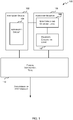
- FIG. 1 illustrates an example system 100 for exhaustively assessing the performance of a hardware design for an integrated circuit to complete a task.
- the system 100 comprises a hardware design 102 for an integrated circuit 104; a hardware monitor 106 comprising monitoring and counting logic 108 for monitoring events in the hardware design 102 and counting the number of cycles between a start event and a stop event, and property evaluation logic 110 for evaluating one or more formal properties related to the counted number of cycles to assess the performance of the hardware design 102 in completing the task; and a formal verification tool 112 configured to use the hardware monitor 106 to exhaustively assess the performance of the hardware design 102 in completing the task.
- the term "hardware design” is used herein to refer to a description of an integrated circuit for all or part of an electronic system (e.g. a processor) which can be used to generate a hardware manifestation of the integrated circuit (e.g. the hardware design may be synthesised into silicon or used to program a field-programmable gate array (FPGA)).
- the hardware design may relate to a module, block, unit, sub-system, system or any combination thereof of an electronic system (e.g. processor).
- the hardware design 102 may be implemented in a high level hardware description language (HDL), such as, but not limited to, a register transfer language (RTL).
- HDL hardware description language
- RTL register transfer language
- register transfer languages include, but are not limited to, VHDL (VHSIC Hardware Description Language) and Verilog. It will be evident to a person of skill in the art that other high level hardware description languages may be used such as proprietary high level hardware description languages.
- the integrated circuit 104 defined by the hardware design 102 is configured to perform one or more tasks.
- the term "task” is used herein to mean any transaction that is executed by the integrated circuit 104 that has an identifiable start state and an identifiable end state.
- a task may include, but is not limited to, completion of a stage of the pipeline - e.g. fetching an instruction from a memory or an instruction cache; reconciling branch instructions (e.g. identifying the target of a branch instruction); decoding a specific instruction; executing a specific instruction; or writing back the results of an executed instruction to memory or register(s).
- the hardware monitor 106 is a module configured to: monitor the operation of the hardware design 102 to identify the start and end of a symbolic task; count the number of cycles (e.g. clock cycles) between start of the symbolic task and end of the symbolic task; and, assess the performance of the hardware design 102 in performing the symbolic task based on the counted number of cycles.
- cycles e.g. clock cycles
- the hardware monitor 106 comprises monitoring and counting logic 108 and property evaluation logic 110.
- the monitoring and counting logic 108 is configured to monitor one or more control signals and/or data signals of the hardware design 102 to identify the start and end of a symbolic task; and to count the number of cycles (e.g. clock cycles) between the start and end of the symbolic task.
- a task is a transaction executed by the integrated circuit that has an identifiable start state and an identifiable end state.
- a task may be execution of an instruction with a particular operational code (opcode), and the start of the task may be when an instruction with the particular opcode has been decoded, and the end of the task may be when the instruction with the particular opcode has been executed.
- opcode operational code
- a task may be addition of a and b when a and b are specific values and the start of the task may be when the specific values appear on the input of the adder, and the end of the task may be when the corresponding output appears.
- a symbolic task is a means of representing a set or group of tasks using one or more symbolic variables.
- a symbolic variable represents a set of, or a plurality of, values (also referred to as scalar values which are defined by a specific combination of zeros and ones).
- a symbolic task may be an execution of an instruction with a symbolic opcode where the symbolic opcode represents all of the possible opcodes (e.g. all of the possible scalar opcodes). In this way the symbolic task represents execution of all instructions with any possible opcode.
- a symbolic task may be addition of symbolic input a and symbolic input b, where the symbolic input a represents all possible values of input a (e.g. all of the possible scalar inputs) and symbolic input b represents all possible values of input b (e.g. all of the possible scalar inputs).
- the symbolic task represents the addition of all possible input values.
- a symbolic variable allows a plurality of states to be represented or encoded at once. This may allow the state space to be traversed much more efficiently by considering a number of states at a single step.
- An example implementation of the monitoring and counting logic 108 will be described with reference to FIG. 3 .
- the property evaluation logic 110 evaluates one or more formal properties based on the counted number of cycles to assess the performance of the hardware design 102 in completing the symbolic task.
- the one or more properties may, for example, be configured to verify whether a performance goal is met (e.g. that the hardware design 102 always complete the tasks within a predetermined number of clock cycles) or to identify a performance metric of the hardware design 102 in completing the task (e.g. the maximum number of clock cycles to complete the task).
- a formal property is a statement or expression that captures design behavior.
- a formal property is an executable statement that checks for specific behavior within the HDL design. For example, if a design contains a FIFO (first in first out) buffer a formal property may be that neither overflow nor underflow of the FIFO may occur.
- Formal properties are used to capture required or desired temporal behavior of the hardware design in a formal and unambiguous way.
- the hardware design can then be verified to determine that it conforms to the required or desired behavior as captured by one or more properties.
- assertion language which also may be referred to as a property language, captures the design behavior over multiple design cycles in a concise, unambiguous manner. While traditional hardware description languages (HDL), such as VHDL or Verilog RTL, have the ability to capture individual cycle behavior, they are too detailed to describe properties at a higher level. In particular, assertion languages provide means to express temporal relationships and complex design behaviors in a concise manner.
- HDL hardware description languages
- Assertion languages include, but are not limited to, SystemVerilog Assertions (SVA), Property Specification Language (PSL), Incisive® Assertion Library (IAL), Synopsys® OpenVeraTM Assertions (OVA), Symbolic Trajectory Evaluation (STE), Hardware Property Language (HPL), 0-In®, and Open Verification Library (OVL).
- SVA SystemVerilog Assertions
- PSL Property Specification Language
- IAL Incisive® Assertion Library
- OVA Synopsys® OpenVeraTM Assertions
- STE Symbolic Trajectory Evaluation
- HPL Hardware Property Language
- 0-In® 0-In®
- OTL Open Verification Library
- a formal property may be asserted or covered. When a formal property is asserted it must always be true. In contrast, when a property is covered the property must be true at least once, but is not required to be true always.
- An asserted property is said to form an assertion.
- a covered property is said to form a cover.
- Formal properties are typically 'clocked', meaning that they are only evaluated upon a clock event occurring (e.g. upon the positive edge of a clock signal or the negative edge of a clock signal). Accordingly, assertions or covers generally indicate which clock and which clock edge triggers evaluation of the formal property.
- the property evaluation logic 110 is configured to evaluate at least one formal property related to the counted number of cycles (e.g. clock cycles) between start and end of a symbolic task to verify a performance goal and/or to identify a performance metric related to the symbolic task.
- the counted number of cycles e.g. clock cycles
- the property evaluation logic 110 may be configured to evaluate an assertion.
- the performance goal is that the hardware design 102 always executes the task within a predetermined number of clock cycles
- the property evaluation logic 110 may be configured to evaluate an assertion that asserts that the counted number of clock cycles is less than the predetermined number of clock cycles.
- the property evaluation logic 110 may be configured to evaluate an assertion that the counted number of clock cycles is less than or equal to N where N is the worst case allowed performance for the task.
- the property evaluation logic 110 may be configured to evaluate one or more assertions or covers to identify the performance metric.
- the property evaluation logic 110 may be configured to evaluate a plurality of covers each of which states that the counted number of clock cycles is equal to a different number within a range of numbers. For example, the property evaluation logic 110 may be configured to evaluate a cover that states the counter is equal to 20, a cover that states the counter is equal to 21, a cover that states that the counter is equal to 22, and so on up to a cover that states the counter is equal to 30. In this way, if the worst case performance is likely to be between 20 and 30 cycles the exact number between 20 and 30 can be identified.
- the property evaluation logic 110 may be configured to evaluate a cover that states that the counter is greater than 20 and less than or equal to 30.
- the property evaluation logic 110 may be configured to evaluate any number of assertions and/or covers to assess the performance of a hardware design in completing a task (i.e. to verify a performance goal and/or to identify a performance metric).
- the hardware monitor 106 may be implemented in software.
- the hardware monitor 106 may be implemented using a hardware description language (HDL) or an assertion language (e.g. SystemVerilog Assertions (SVA)).
- HDL hardware description language
- SVA SystemVerilog Assertions
- the hardware monitor 106 is bound to the hardware design 102 to monitor the completion of tasks. Where the hardware monitor 106 is implemented in SVA and the hardware design 102 is implemented in RTL, the SVA code is bound to the RTL code.
- the hardware design 102 e.g. RTL
- hardware monitor 106 e.g. SVA
- bindings are loaded into a formal verification tool 112.
- the formal verification tool 112 is a software tool that is capable of performing formal verification of a hardware design. Examples of formal verification tools include, but are not limited to, Mentor Graphics Questa® Formal Verification, Synopsys VC Formal, Cadence® Incisive® Enterprise Verifier, JasperGold®, and OneSpin 360 DVTM.
- Formal verification is a systematic process that uses mathematical reasoning to verify a property in a hardware design. Formal verification can be contrasted to simulation-based verification in which a hardware design is tested by applying stimuli to the hardware design and monitoring the output of the hardware design in response to the stimuli.
- the hardware design e.g. hardware design 102
- a mathematical model e.g. a state-transition system
- formal properties e.g. those evaluated by the property evaluation logic 110
- a formal property is verified by searching the entire reachable state space of the hardware design (e.g. state transition system) without explicitly traversing the state machine.
- the search is done by, for example, encoding the states using efficient Boolean encodings using Binary decision diagrams (BDDS), or using advanced SAT (satisfiability-based bounded model checking) based techniques.
- BDDS Binary decision diagrams
- advanced SAT satisfiability-based bounded model checking
- tools can be used to implement techniques, such as, but not limited to, abstraction, symmetry, symbolic indexing, and invariants to improve performance and achieve scalability.
- a formal property that is covered is verified by searching the reachable state space of the hardware design (e.g. state transition system) for at least one valid state (as defined by formal constraints) in which the property is true. Once a valid state is found in which the property is true then the searching ceases.
- a formal property that is asserted is verified by confirming the property is true for all valid states (as defined by formal constraints).
- an asserted property is verified by searching the reachable state space of the hardware design for a valid state in which the property is not true. Since formal verification of an asserted property algorithmically and exhaustively explores all valid input values over time, verifying an asserted property in this manner allows a property to be exhaustively proved or disproved for all valid states.
- the formal verification tool 112 may output an indication of whether or not the assertion is valid (i.e. is true for all valid states), which may also be referred to herein as the assertion being successfully verified.
- the output may be yes the assertion is valid or has been successfully verified; no the assertion is not valid (i.e. it is not true or has failed for at least one valid state) or has not been successfully verified; or the formal verification was inconclusive.
- the formal verification may be inconclusive, for example, because the computing-based device running the formal verification tool 112 has run out of memory or because the formal verification tool 112 has determined that a certain amount of progress has not been made after a predefined period of time.
- the formal verification tool 112 may output information indicating a state of the hardware design in which the assertion was false. For example, the formal verification tool 112 may output a trace of the verification indicating at what point or state the failure occurred.
- the formal verification tool 112 is configured to formally verify the one or more properties defined in the hardware monitor 106 hold or are true for all of the tasks covered by the symbolic task. For example, where the symbolic task is execution of an instruction with a symbolic opcode, the formal verification tool 112 is configured to formally verify the one or more properties defined in the hardware monitor 106 hold for each possible opcode.
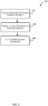
- FIG. 2 illustrates a flow diagram of an example method 200 for exhaustively assessing the performance of a hardware design 102 in completing a task.
- the method 200 may be implemented on a computing-based device, such as the computing-based device 700 described below with reference to FIG. 7 .
- the method 200 begins at block 202 where the hardware design 102 and the hardware monitor 106 are received at the computing-based device 700.
- the hardware design 102 defines an integrated circuit to perform one or more tasks; and the hardware monitor 106 is configured to count the number of cycles (e.g. clock cycles) between starting and completing a symbolic task, and assess the performance of the hardware design in completing the task by evaluating one or more formal properties related to the counted number of cycles (e.g. clock cycles).
- one or more of the formal properties in the hardware monitor 106 may be asserted and/or one or more of the formal properties in the hardware monitor 106 may be covered. Where a property is asserted it must be true for all possible states and where a property is covered it must be true at least once, but does not have to always be true.
- the specific properties and whether they are asserted or covered are configured to provide an exhaustive assessment of the performance of the hardware design in completing the task.
- the assessment may be an exhaustive verification that the hardware design meets a performance goal (e.g. always completes the task within a predetermined number of clock cycles); or may be identification of a performance metric (e.g. a minimum or maximum number of clock cycles to complete the task).
- the formal verification tool 112 formally verifies that the properties defined in the hardware monitor 106 hold (or are true) for the hardware design 102.
- Formally verifying an asserted property comprises verifying that for all valid states of the hardware design 102 (as defined by the formal constraints) that the property is true. For example, verifying an assertion that the counted number of clock cycles is less then N comprises determining whether there is a state of the hardware design 102 wherein the counted number of clock cycles is greater than or equal to N.
- an asserted property relates to a symbolic variable (e.g. a symbolic task)
- formally verifying the asserted property comprises verifying that the property is true for all valid values of the symbolic variable.
- the formal verification tool 112 exhaustively verifies the property for all possible values of the symbolic variable.
- the symbolic task is execution of an instruction with a symbolic opcode representing all possible opcodes
- the hardware monitor defines an assertion that the counter (representing the number of clock cycles to execute the instruction with the symbolic opcode) is less than a predetermined number of clock cycles
- the formal verification tool 112 verifies that for all instructions with a possible opcode the counter is less than the predetermined number of clock cycles. If there is even one instruction with any possible opcode where the counter is greater than or equal to the predetermined number of clock cycles then the assertion will fail.
- Formally verifying a covered property comprises verifying that there is at least one valid state of the hardware design 102 (as defined by the formal constraints) that the property is true. For example, verifying a cover that the counted number of clock cycles is equal to N comprises determining whether there is a state of the hardware design 102 wherein the counted number of clock cycles is equal to N.
- a covered property relates to a symbolic variable (e.g. a symbolic task) the cover will be verified if the formal verification tool 112 can identify, for any possible value of the symbolic variable, that the property is true.
- the symbolic task is an execution of an instruction with a symbolic opcode representing all possible opcodes
- the hardware monitor 106 defines a cover that the counter (representing the number of clock cycles to execute the instruction with the symbolic opcode) is equal to a predetermined number
- the formal verification tool 112 is able to identify an instruction with any possible opcode where the counter is equal to the predetermined number then the cover will be verified.
- the formal verification tool 112 outputs an indication of whether the properties were successfully verified or not.
- This indication provides an assessment of the performance of the hardware design 102 in completing the task.
- the indication may: prove that the hardware design 102 meets a performance goal; and/or identify a performance metric (e.g. the minimum number of clock cycles to complete the task and/or the maximum number of clock cycles to complete the task).
- the formal verification tool 112 may output an indication that it has been successfully verified (i.e. that it is true for all possible states) or that it has not been successfully verified (i.e. that it is not true for at least one state). Where the asserted property has not been successfully verified the formal verification tool 112 may also output an indication of a state of the hardware design 102 in which the property was not true. Similarly where the property is covered the formal verification tool 112 may output an indication that it has been successfully verified (i.e. that it is true for a least one state) or that it has not been successfully verified (i.e. that it is not true for any state). Where the covered property has been successfully verified the formal verification tool 112 may also output an indication of a state of the hardware design 102 in which the property was true.
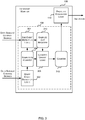
- the hardware monitor 106 comprises monitoring and counting logic 108 for counting the cycles (e.g. clock cycles) between the start and end of a symbolic task in a hardware design 102; and property evaluation logic 110 for evaluating one or more formal properties based on the count of cycles (e.g. clock cycles) to assess the performance of the hardware design 102 in completing the task.
- cycles e.g. clock cycles
- property evaluation logic 110 for evaluating one or more formal properties based on the count of cycles (e.g. clock cycles) to assess the performance of the hardware design 102 in completing the task.
- the monitoring and counting logic 108 comprises start event detection logic 302 for detecting the start of a symbolic task in the hardware design 102; end event detection logic 304 for detecting the completion of the symbolic task in the hardware design 102; and counter update logic 306 for counting the number of clock cycles between the start event and the end event.
- the start event detection logic 302 monitors one or more control signals and/or data signals of the hardware design 102 to detect a start event indicating the start of a symbolic task.
- the specific control signals and/or data signals that will be monitored, and the status thereof indicating a start event has occurred, will vary depending on the task being monitored and the configuration of the hardware design 102.
- the start event detection logic 302 may be configured to monitor the output of a fetch stage or a decode stage of the processor to determine when a symbolic instruction has been fetched or decoded.
- the start event detection logic 302 may set a sampled in register 308 to indicate that the task has started.
- the end event detection logic 304 monitors one or more control signals and/or data signals of the hardware design 102 to detect an end event indicating the completion of the symbolic task in the hardware design 102.
- the specific control signals and/or data signals that will be monitored, and the status thereof indicating an end event has occurred, will vary depending on the task being monitored and the configuration of the hardware design 102.
- the end event detection logic 304 may be configured to monitor the output of an execution stage of the processor to determine when a symbolic instruction has been executed.
- the end event detection logic 304 may set a sampled out register 310 to indicate that the task has been completed.
- the end event detection logic 304 is configured to only set the sampled out register if it detects the end event and the start event has already been detected.
- the end event detection logic 304 may be configured to determine that the start event has been detected based on the status of the sampled in register 308. For example, in some cases, the end event detection logic 304 may be configured to only set the sampled out register 310 if the end event is detected and the sampled in register 308 is set.
- the counter update logic 306 is configured to count the number of cycles (e.g. clock cycles) between the start event and the end event. In other words, the counter update logic 306 counts the number of cycles (e.g. clock cycles) it takes to complete the symbolic task defined by the start event and the end event.
- the counter update logic 306 may be configured to, each cycle (e.g. clock cycle), determine whether the start event has been detected (e.g. from the state of the sampled in register 308). If the start event has been detected then the counter update logic 306 may be configured to determine whether the end event has been detected (e.g. from the state of the sampled out register 310). If the end event has not been detected then the counter update logic 306 may increment a counter 312. If, however, the end event has been detected then the counter update logic 306 does not increment the counter 312.
- the property evaluation logic 110 evaluates (e.g. periodically, such as, each cycle) one or more properties related to the value of the counter 312 to assess the performance of the hardware design in completing the task.
- the assessment may be, for example, verification that the hardware design always performs the task within a predetermined number of clock cycles; or identification of a performance metric (e.g. the minimum and/or maximum number of clock cycles for the hardware design 102 to complete the task).
- the property may state or express that the counter 312 is less than or equal to N.
- a property may be asserted or covered. If the property evaluation logic 110 determines that an asserted property is not true then the property evaluation logic 110 may output an indication that the property is not true. Conversely, if the property evaluation logic 110 determines that a covered property is true then the property evaluation logic 110 may output an indication that the property is true.
- the logic blocks may be triggered by a clock.
- the logic blocks may be triggered by the rising or positive edge of the clock.
- one or more of the logic blocks may be combined or their functionality may divided between logic blocks in another manner.
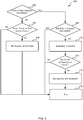
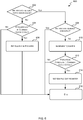
- FIG. 4 illustrates an example method 400 for assessing the performance of a hardware design in completing a symbolic task which may be implemented by the hardware monitor 106 of FIG. 3 each cycle (e.g. clock cycle).
- the method 400 begins at block 402 where the start event detection logic 302 determines whether a start event has already been detected.
- the start event detection logic 302 may be configured to determine whether a start event has already been detected based on the state of the sampled in register 308. If the start event detection logic 302 determines that a start event has already been detected then the method proceeds to block 408. If, however, the start event detection logic 302 determines that a start event has not already been detected then the method 400 proceeds to block 404.
- the start event detection logic 302 determines whether a start event has occurred in the current cycle (e.g. clock cycle). In some cases determining whether a start event has occurred in the current cycle (e.g. clock cycle) comprises sampling one or more controls signals and/or data signals of the hardware design 102 and determining whether the one or more control signals and/or data signals are in a predetermined state. The specific control signals and/or data signals, and the state or configuration thereof, that indicate a start event depends on the particular task being assessed and the configuration of the hardware design 102.
- start event detection logic 302 determines that a start event has occurred in the current cycle (e.g. clock cycle) then the method 400 proceeds to block 406. If, however, the start event detection logic 302 determines that a start event has not occurred in the current cycle (e.g. clock cycle) then the method 400 ends 416.
- the start event detection logic 302 sets the sampled in register 308 to indicate that a start event has been detected.
- the start event detection logic 302 is configured to set the sampled in register 308 to "1" to indicate that a start event has been detected.
- the sampled in register 308 can be set to any other value to indicate that a start event has been detected.
- the end event detection logic 304 determines whether an end event has already been detected.
- the end event detection logic 304 may be configured to determine whether an end event has already been detected based on the state of the sampled out register 310. If the end event detection logic 304 determines that an end event has already been detected then the method 400 ends 416. If, however, the end event detection logic 304 determines that an end event has not already been detected then the method 400 proceeds to block 410.
- the counter update logic 306 increments the counter 312 to indicate that one additional cycle (e.g. clock cycle) has elapsed since the start event was detected and before the end event was detected. Once the counter update logic 306 has incremented the counter 312, the method 400 proceeds to block 412.
- one additional cycle e.g. clock cycle
- the end event detection logic 304 determines whether an end event has occurred in the current cycle (e.g. clock cycle). In some cases, determining whether an end event has occurred in the current cycle (e.g. clock cycle) comprises sampling one or more controls signals and/or data signals and determining whether one or more control signals and/or data signals are in a predetermined state. The specific control signals and/or data signals, and the state or configuration thereof, that indicate an end event depends on the particular task being assessed and the configuration of the hardware design 102.
- the method 400 proceeds to block 414. If, however, the end event detection logic 304 determines that an end event has not occurred in the current cycle (e.g. clock cycle) then the method 400 ends 416.
- the end event detection logic 304 sets the set sampled out register 310 to indicate that an end event has been detected.
- the end event detection logic 304 is configured to set the sampled out register 310 to "1" to indicate that an end event has been detected.
- the sampled out register 310 can be set to any other value to indicate that an end event has been detected.
- FIG. 5 illustrates an example implementation of a hardware monitor 500 (which can be used as hardware monitor 106 of FIG. 1 ) for assessing the performance of a hardware design 502 for a processor 504 in executing instructions.
- a processor fetches instructions from a program, decodes the fetched instructions, executes the decoded instructions, and stores the results of the executed instructions in memory and/or registers.
- the hardware monitor 500 like the hardware monitor 106 of FIGS. 1 and 3 , comprises monitoring and counting logic 514 and property evaluation logic 516.
- the monitoring and counting logic 514 is configured to detect when a start event has occurred and when a stop event has occurred; and count the number of cycles between the start event and the stop event.
- the start event is either when a symbolic instruction has been fetched or when a symbolic instruction has been decoded
- the end event is when the symbolic instruction has been executed.
- the monitoring and counting logic 514 then counts the number of clock cycles between the symbolic instruction being fetched (or decoded) and the symbolic instruction being executed.
- the monitoring and counting logic 514 comprises start instruction execution detection logic 518 for detecting that a symbolic instruction has been fetched (or that a symbolic instruction has been decoded); end instruction execution detection logic 520 for detecting that the symbolic instruction has been executed; and counter update logic 522 for counting the number of clock cycles between the fetch/decode of the symbolic instruction and execution of the symbolic instruction.
- the start instruction execution detection logic 518 is configured to monitor one or more control signals and/or data signals of the hardware design 502 to detect when a symbolic instruction has been fetched (or when a symbolic instruction has been detected).
- the symbolic instruction is an instruction with a particular opcode.
- the start instruction execution detection logic 518 may be configured to detect that the symbolic instruction has been fetched/decoded when an instruction with the particular opcode has been fetched/decoded.
- the symbolic instruction may be defined by another property, such as instruction address.
- start instruction execution detection logic 518 When the start instruction execution detection logic 518 detects the start event (i.e. that the symbolic instruction has been fetched or decoded) the start instruction execution detection logic 518 may set a sampled in register 524 to indicate that the task (execution of the instruction) has started.
- the start instruction execution detection logic 518 may be configured to detect that the symbolic instruction has been decoded when the processor is currently decoding an instruction with the particular opcode.
- SVA code for implementing such start event detection logic where sampled_in is the sampled in register 524, current_state is the current state of the processor (e.g. fetching, decoding, or executing), opcode is the opcode of the instruction currently being processed by the processor 504:
- start instruction execution detection logic 518 may be configured to detect that a symbolic instruction has been decoded in another manner.
- the start instruction execution detection logic 518 may be configured to monitor the output of a decode stage of the processor to detect when the decode stage outputs an instruction with the specific opcode (or other specific feature).
- the end instruction execution detection logic 520 is configured to monitor one or more control signals and/or data signals of the hardware design 502 to detect when the symbolic instruction has been executed.
- a symbolic instruction is an instruction with a particular opcode.
- the end instruction execution detection logic 520 may be configured to detect that the symbolic instruction has been executed when the instruction with the particular opcode has been executed.
- the symbolic instruction may be defined by another property, such as instruction address or other identification information.
- the end instruction execution detection logic 520 When the end instruction execution detection logic 520 detects the end event (i.e. that the symbolic instruction has been executed) the end instruction execution detection logic 520 may set a sampled out register 526 to indicate that the task (execution of the instruction) has been completed.
- the end instruction execution detection logic 520 is configured to only update the sampled out register 526 if the end event (i.e. execution of the symbolic instruction) is detected and the start event (i.e. the symbolic instruction has been fetched/decoded) has already been detected.
- the end instruction execution detection logic 520 may be configured to determine that the start event has been detected based on the status of the sampled in register 524. For example, in some cases, the end instruction execution detection logic 520 may be configured to only set the sampled out register 526 if the sampled in register 524 is set and the end event is detected.
- the processor processes a single instruction at a time the end instruction execution detection logic 520 may be configured to detect that the symbolic instruction has been executed when the processor fetches a new instruction.
- the following is example SVA code for implementing such end event detection logic where sampled_in is the sampled in register 524, current_state is the current state of the processor (e.g. fetching, decoding, executing), and sampled_out is the sampled out register 526:
- the end instruction execution detection logic 520 may be configured to detect that the symbolic instruction has been executed in another manner.
- the end instruction execution detection logic 520 may be configured to monitor the output of an execution stage of the processor to detect when the execution stage outputs an instruction with the specific opcode (or other specific feature).
- the counter update logic 522 is configured to count the number of clock cycles between the start event and the end event - i.e. between the symbolic instruction being fetched/decoded and the symbolic instruction being executed. In other words, the counter update logic 522 counts the number of clock cycles it takes for the processor to execute the symbolic instruction.
- the counter update logic 522 may be configured to determine in each clock cycle whether the start event (i.e. fetch/decode of the symbolic instruction) has been detected (e.g. from the state of the sampled in register 524). If the start event (i.e. fetch/decode of the symbolic instruction) has been detected then the counter update logic 522 may be configured to determine whether the end event (i.e. execution of the symbolic instruction) has been detected (e.g. from the state of the sampled out register 526). If the end event (i.e. execution of the symbolic instruction) has not been detected then the counter update logic 522 may increment a counter 528. If, however, the end event has been detected then the counter update logic 522 does not increment the counter 528.
- start event i.e. fetch/decode of the symbolic instruction
- the counter update logic 522 may be configured to determine whether the end event (i.e. execution of the symbolic instruction) has been detected (e.g. from the state of the sampled out register 526). If the end event (i.e.
- SVA code for implementing counter update logic 522 that is configured to increment the counter 528 for each clock cycle in which the sampled in register 524 is set and the sampled out register 526 is not set.
- sampled_in is the sampled in register 524
- sampled_out is the sampled out register 526
- latency_counter is the counter 528:
- the above SVA code causes the counter (latency_counter) to be set to zero after a reset (! resetn), and incremented by one if the sampled in register (sampled_in) is set and the sampled out register (sampled_out) is not set. It will be evident to a person of skill in the art that this is an example only and the counter update logic 522 may be configured to update the counter in another manner.
- the property evaluation logic 516 evaluates (e.g. periodically, such as, each clock cycle) one or more properties related to the value of the counter 528 to assess the performance of the hardware design 502 in executing instructions.
- the property evaluation logic 516 may be configured to verify that the hardware design 502 executes instructions within a predetermined number of clock cycles.
- the property evaluation logic may be configured to evaluate an assertion that asserts the counter is less than a predetermined number of clock cycles.
- SVA code for implementing property evaluation logic 516 that evaluates an assertion that the counter is less than a predetermined number of clock cycles.
- latency_counter is the counter 528 and N is the predetermined number of clock cycles.
- the formal verification tool 122 typically stops the verification as soon as it finds a state of the hardware design 502 in which the assertion fails (i.e. a state in which the counter is greater than or equal to N). Accordingly, the formal verification tool 112 typically only provides information on the one state of the hardware design 502 it identified in which the assertion is not true. Therefore, in some cases, to get more granular feedback (or information) from the formal verification tool 112, the property evaluation logic 516 may be configured to evaluation a plurality of assertions which each assert that the property (e.g. the counter is less than N) is true for a particular symbolic instruction (e.g. a particular opcode). The formal verification tool 112 will then formally verify each assertion and provide feedback if any of the assertions fail. This allows the developer or engineer to know which types of instructions are problematic (e.g. not meeting the performance goal).
- SVA code for implementing property evaluation logic 516 that is configured to evaluate an assertion for each possible opcode (in this case there are 64 possible opcodes) that asserts that when the opcode of the symbolic instruction is that possible opcode the counter is less than a predetermined number of clock cycles.
- latency_counter is the counter 528 and N is the predetermined number of clock cycles.
- the above SVA code causes the property evaluation logic to generate sixty-four assertions that each assert that when the opcode is a particular value then the counter (latency_counter) is less than the predetermined number of clock cycles (N).
- Formal verification of such a set of assertions can be used to not only prove that the hardware design 502 executes all instructions within a predetermined number of clock cycles, but, it can also provide granular feedback of which types of instructions are not being executed within the predetermined number of clock cycles.
- the property evaluation logic 516 may be configured to identify performance metrics (e.g. best and/or worst case performance) of the hardware design 502 in executing instructions. For example, where the hardware monitor 500 is being used to identify the maximum number of clock cycles to execute instructions then the property evaluation logic 516 may be configured to evaluate a plurality of covers each of which state that the counted number of clock cycles is equal to a different number within a range of numbers. For example, the property evaluation logic 516 may be configured to evaluate a cover that states the counter is equal to 20, a cover that states the counter is equal to 21, a cover that states that the counter is equal to 22, and so on up to a counter that states the counter is equal to 30. In this way, if the worst case performance is likely to be between 20 and 30 the exact number between 20 and 30 can be identified.
- performance metrics e.g. best and/or worst case performance
- latency_counter is the counter 528.
- the above SVA code causes the property evaluation logic 516 to generate one hundred covers that state that the counter (latency_counter) is equal to a different value between 0 and ninety-nine. Formal verification of such a set of covers can be used to identify the maximum number of clock cycles it takes the hardware design 502 to execute any instruction with any opcode.
- the formal verification tool 112 searches the state space of the hardware design 102 to identify a state in which the property is true.
- FIG. 6 illustrates an example method 600 for assessing the performance of a hardware design for a processor in executing instructions, which may be implemented by the hardware monitor 500 of FIG. 5 each clock cycle.
- the method 600 generally corresponds to method 400 of FIG. 4 .
- the method 600 begins at block 602 where the start instruction execution detection logic 518 determines whether the symbolic instruction has already been fetched (or decoded) (e.g. based on the state of the sampled in register 524).
- the start instruction execution detection logic 518 determines whether the symbolic instruction has been fetched (or decoded) in the current clock cycle (e.g. based on one or more control signals and/or data signals of the processor). If the start instruction execution detection logic 518 determines that the symbolic instruction has been fetched/decoded in the current clock cycle then at block 606 the sampled in register 524 is set to indicate the start event has been detected, otherwise the method 600 ends 616.
- the end instruction execution detection logic 520 determines whether the symbolic instruction has already been executed (e.g. based on the sampled out register 526). If the symbolic instruction has already been executed then the method 600 ends 616.
- the counter update logic 522 increments the counter 528 to indicate that one more clock cycle has elapsed since the symbolic instruction has been fetched (or decoded). Then at block 612 the end instruction execution detection logic 520 determines whether the symbolic instruction has been executed in the current clock cycle (e.g. based on one or more control signals and/or data signals of the processor). If the symbolic instruction has not been executed in the current clock cycle then the method 600 ends 616. Otherwise, at block 614 the end instruction execution detection logic 520 sets the set sampled out register 526 to indicate that an end event has been detected. The method 600 then ends 616.
- the hardware monitor 106 or 500 may be synthesised into hardware (e.g. an integrated circuit) as part of, or in connection with, the hardware design 102 or 502.
- the properties of the hardware monitor 106 or 500 act as a monitor during operation of the hardware (e.g. integrated circuit 104 or processor 504).
- the hardware monitor 106 or 500 evaluates the properties (e.g. upon the positive edge of the clock signal).
- any symbolic variable is typically implemented by a register which has a fixed value during operation.
- the fixed value may be randomly assigned each time the hardware monitor 106 or 500 is reset.
- the symbolic opcode may be assigned opcode 0 after a first reset of the hardware monitor 106 or 500
- the symbolic opcode may be assigned opcode 3 after a second reset of the hardware monitor 106 or 500. Accordingly, after the first reset, the hardware monitor 106. 300, 500, or 700 monitors instructions with opcode 0, and after the second reset, the hardware monitor 106, or 500 monitors instructions with opcode 3.
- the hardware monitor 106 or 500 may be configured to output information indicating whether or not the properties are true or not.
- the hardware monitor 106 or 500 may be configured to, upon detecting that an asserted property has failed (or is not true), output information indicating that the assertion has failed and/or the state at which the assertion failed.
- the hardware monitor 106 or 500 may be configured to, upon detecting that a covered property is valid (or is true), output information indicating that the cover is true and/or the state at which the cover was true.
- the output information can provide an assessment of the performance of the hardware design in completing the task.
- the information may: indicate that the hardware design does or does not meet a performance goal; and/or identify a performance metric (e.g. the minimum number of clock cycles to complete the task and/or the maximum number of clock cycles to complete the task).
- a performance metric e.g. the minimum number of clock cycles to complete the task and/or the maximum number of clock cycles to complete the task.
- FIG. 7 illustrates various components of an exemplary computing-based device 700 which may be implemented as any form of a computing and/or electronic device, and in which embodiments of the systems, methods and hardware monitors described above may be implemented.
- Computing-based device 700 comprises one or more processors 702 which may be microprocessors, controllers or any other suitable type of processors for processing computer executable instructions to control the operation of the device in order to assess the performance of a hardware design in completing a task.
- the processors 702 may include one or more fixed function blocks (also referred to as accelerators) which implement a part of the method of assessing the performance of a hardware design in completing a task in hardware (rather than software or firmware).
- Platform software comprising an operating system 704 or any other suitable platform software may be provided at the computing-based device to enable application software, such as a formal verification tool 112, to be executed on the device.
- Computer-readable media may include, for example, computer storage media such as memory 706 and communications media.
- Computer storage media i.e. non-transitory machine readable media
- memory 706 includes volatile and non-volatile, removable and non-removable media implemented in any method or technology for storage of information such as computer readable instructions, data structures, program modules or other data.
- Computer storage media includes, but is not limited to, RAM, ROM, EPROM, EEPROM, flash memory or other memory technology, CD-ROM, digital versatile disks (DVD) or other optical storage, magnetic cassettes, magnetic tape, magnetic disk storage or other magnetic storage devices, or any other non-transmission medium that can be used to store information for access by a computing device.
- communication media may embody computer readable instructions, data structures, program modules, or other data in a modulated data signal, such as a carrier wave, or other transport mechanism.
- computer storage media does not include communication media.
- the computer storage media i.e. non-transitory machine readable media, e.g. memory 706
- the storage may be distributed or located remotely and accessed via a network or other communication link (e.g. using communication interface 708).
- the computing-based device 700 also comprises an input/output controller 710 arranged to output display information to a display device 712 which may be separate from or integral to the computing-based device 700.
- the display information may provide a graphical user interface.
- the input/output controller 710 is also arranged to receive and process input from one or more devices, such as a user input device 714 (e.g. a mouse or a keyboard). This user input may be used to, for example, initiate formal verification of the properties define din the hardware monitor 106.
- the display device 712 may also act as the user input device 714 if it is a touch sensitive display device.
- the input/output controller 710 may also output data to devices other than the display device, e.g. a locally connected printing device (not shown in FIG. 7 ).
- the hardware monitors of FIGS. 3 and 5 are shown as comprising a number of functional blocks. This is schematic only and is not intended to define a strict division between different logic elements of such entities. Each functional block may be provided in any suitable manner. It is to be understood that intermediate values described herein as being formed by a hardware monitor need not be physically generated by the hardware monitor at any point and may merely represent logical values which conveniently describe the processing performed by the hardware monitor between its input and output.
- Computer program code and computer readable instructions refer to any kind of executable code for processors, including code expressed in a machine language, an interpreted language or a scripting language.
- Executable code includes binary code, machine code, bytecode, code defining an integrated circuit (such as a hardware description language or netlist), and code expressed in a programming language code such as C, Java or OpenCL.
- Executable code may be, for example, any kind of software, firmware, script, module or library which, when suitably executed, processed, interpreted, compiled, executed at a virtual machine or other software environment, cause a processor of the computer system at which the executable code is supported to perform the tasks specified by the code.
- a processor, computer, or computer system may be any kind of device, machine or dedicated circuit, or collection or portion thereof, with processing capability such that it can execute instructions.
- a processor may be any kind of general purpose or dedicated processor, such as a CPU, GPU, System-on-chip, state machine, media processor, an application-specific integrated circuit (ASIC), a programmable logic array, a field-programmable gate array (FPGA), physics processing units (PPUs), radio processing units (RPUs), digital signal processors (DSPs), general purpose processors (e.g. a general purpose GPU), microprocessors, any processing unit which is designed to accelerate tasks outside of a CPU, etc.
- a computer or computer system may comprise one or more processors. Those skilled in the art will realize that such processing capabilities are incorporated into many different devices and therefore the term 'computer' includes set top boxes, media players, digital radios, PCs, servers, mobile telephones, personal digital assistants and many other devices.
- a hardware design which also may be referred to herein as an integrated circuit definition data set, describes an integrated circuit to perform one or more tasks.
- the hardware design may be implemented in software, such as HDL (hardware description language).
- HDL hardware description language
- a computer readable storage medium having encoded thereon computer readable program code in the form of an integrated circuit definition dataset (e.g. hardware design) that when processed in an integrated circuit manufacturing system configures the system to manufacture an integrated circuit to perform the one or more tasks.
- An integrated circuit definition dataset may be in the form of computer code, for example as a netlist, code for configuring a programmable chip, as a hardware description language defining an integrated circuit at any level, including as register transfer level (RTL) code, as high-level circuit representations such as Verilog or VHDL, and as low-level circuit representations such as OASIS (RTM) and GDSII.
- RTL register transfer level
- RTM OASIS
- GDSII GDSI
- one or more intermediate user steps may be required in order for a computer system configured for generating a manufacturing definition of an integrated circuit to execute code defining an integrated circuit so as to generate the manufacturing definition of that integrated circuit.
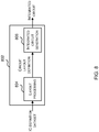
- FIG. 8 shows an example of an integrated circuit (IC) manufacturing system 802 which comprises a layout processing system 804 and an integrated circuit generation system 806.
- the IC manufacturing system 802 is configured to receive an IC definition dataset (e.g. a hardware design 102 or 502 defining an integrated circuit to perform one or more tasks), process the IC definition dataset, and generate an IC according to the IC definition dataset (e.g. hardware design 102 or 502).
- the processing of the IC definition dataset configures the IC manufacturing system 802 to manufacture an integrated circuit to perform one or more tasks.
- the layout processing system 804 is configured to receive and process the IC definition dataset to determine a circuit layout.
- Methods of determining a circuit layout from an IC definition dataset are known in the art, and for example may involve synthesising RTL code to determine a gate level representation of a circuit to be generated, e.g. in terms of logical components (e.g. NAND, NOR, AND, OR, MUX and FLIP-FLOP components).
- a circuit layout can be determined from the gate level representation of the circuit by determining positional information for the logical components. This may be done automatically or with user involvement in order to optimise the circuit layout.
- the layout processing system 804 When the layout processing system 804 has determined the circuit layout it may output a circuit layout definition to the IC generation system 806.
- a circuit layout definition may be, for example, a circuit layout description.
- the IC generation system 806 generates an IC according to the circuit layout definition, as is known in the art.
- the IC generation system 806 may implement a semiconductor device fabrication process to generate the IC, which may involve a multiple-step sequence of photo lithographic and chemical processing steps during which electronic circuits are gradually created on a wafer made of semiconducting material.
- the circuit layout definition may be in the form of a mask which can be used in a lithographic process for generating an IC according to the circuit definition.
- the circuit layout definition provided to the IC generation system 806 may be in the form of computer-readable code which the IC generation system 806 can use to form a suitable mask for use in generating an IC.
- the different processes performed by the IC manufacturing system 802 may be implemented all in one location, e.g. by one party.
- the IC manufacturing system 802 may be a distributed system such that some of the processes may be performed at different locations, and may be performed by different parties.
- some of the stages of: (i) synthesising RTL code representing the IC definition dataset to form a gate level representation of a circuit to be generated, (ii) generating a circuit layout based on the gate level representation, (iii) forming a mask in accordance with the circuit layout, and (iv) fabricating an integrated circuit using the mask may be performed in different locations and/or by different parties.
- processing of the integrated circuit definition dataset at an integrated circuit manufacturing system may configure the system to manufacture an integrated circuit without the IC definition dataset being processed so as to determine a circuit layout.
- an integrated circuit definition dataset may define the configuration of a reconfigurable processor, such as an FPGA, and the processing of that dataset may configure an IC manufacturing system to generate a reconfigurable processor having that defined configuration (e.g. by loading configuration data to the FPGA).
- an integrated circuit definition dataset could include software which runs on hardware defined at the dataset or in combination with hardware defined at the dataset.
- the IC generation system may further be configured by an integrated circuit definition dataset to, on manufacturing an integrated circuit, load firmware onto that integrated circuit in accordance with program code defined at the integrated circuit definition dataset or otherwise provide program code with the integrated circuit for use with the integrated circuit.
- a remote computer may store an example of the process described as software.
- a local or terminal computer may access the remote computer and download a part or all of the software to run the program.
- the local computer may download pieces of the software as needed, or execute some software instructions at the local terminal and some at the remote computer (or computer network).
- a dedicated circuit such as a DSP, programmable logic array, or the like.
- the methods described herein may be performed by a computer configured with software in machine readable form stored on a tangible storage medium e.g. in the form of a computer program comprising computer readable program code for configuring a computer to perform the constituent portions of described methods or in the form of a computer program comprising computer program code means adapted to perform all the steps of any of the methods described herein when the program is run on a computer and where the computer program may be embodied on a computer readable storage medium.
- tangible (or non-transitory) storage media include disks, thumb drives, memory cards etc. and do not include propagated signals.
- the software can be suitable for execution on a parallel processor or a serial processor such that the method steps may be carried out in any suitable order, or simultaneously.
- the hardware components described herein may be generated by a non-transitory computer readable storage medium having encoded thereon computer readable program code.
- Non-transitory media can be volatile or non-volatile.
- volatile non-transitory media include semiconductor-based memory, such as SRAM or DRAM.
- technologies that can be used to implement non-volatile memory include optical and magnetic memory technologies, flash memory, phase change memory, resistive RAM.
- logic refers to structure that performs a function or functions.
- An example of logic includes circuitry that is arranged to perform those function(s).
- circuitry may include transistors and/or other hardware elements available in a manufacturing process.
- transistors and/or other elements may be used to form circuitry or structures that implement and/or contain memory, such as registers, flip flops, or latches, logical operators, such as Boolean operations, mathematical operators, such as adders, multipliers, or shifters, and interconnect, by way of example.
- Such elements may be provided as custom circuits or standard cell libraries, macros, or at other levels of abstraction. Such elements may be interconnected in a specific arrangement.
- Logic may include circuitry that is fixed function and circuitry can be programmed to perform a function or functions; such programming may be provided from a firmware or software update or control mechanism.
- Logic identified to perform one function may also include logic that implements a constituent function or sub-process.
- hardware logic has circuitry that implements a fixed function operation, or operations, state machine or process.
- any reference to 'an' item refers to one or more of those items.
- the term 'comprising' is used herein to mean including the method blocks or elements identified, but that such blocks or elements do not comprise an exclusive list and an apparatus may contain additional blocks or elements and a method may contain additional operations or elements. Furthermore, the blocks, elements and operations are themselves not impliedly closed.
Landscapes
- Engineering & Computer Science (AREA)
- Theoretical Computer Science (AREA)
- Physics & Mathematics (AREA)
- Computer Hardware Design (AREA)
- General Engineering & Computer Science (AREA)
- General Physics & Mathematics (AREA)
- Quality & Reliability (AREA)
- Evolutionary Computation (AREA)
- Geometry (AREA)
- Software Systems (AREA)
- Computing Systems (AREA)
- Mathematical Physics (AREA)
- Debugging And Monitoring (AREA)
Abstract
Description
- While an electronic system (e.g. a processor), or a component thereof, is often designed to have a small area footprint and satisfy a low power requirement, it is also important that the electronic system, or the component thereof, meets desired performance goals (e.g. performs one or more desired tasks within a certain time limit). For example, where the electronic system is a processor it may be desirable that the processor executes instructions within a certain time limit.
- Since it can be costly to discover, only after the electronic system, or the component thereof, is implemented in hardware (e.g. silicon), that it does not meet desired performance goals, it is beneficial to assess the performance characteristics of the hardware design for the electronic system, or the component thereof, prior to implementing the hardware design in hardware. However, the accuracy of known simulation-based methods for assessing the performance of a hardware design depends on the underlying model and the ability to drive sensible stimulus (e.g. through directed tests or indirectly through executing drivers, operating system boot and other system level tests) to measure the response.
- The embodiments described below are provided by way of example only and are not limiting of implementations which solve any or all of the disadvantages of known methods and systems for assessing the performance of a hardware design.
- This Summary is provided to introduce a selection of concepts in a simplified form that are further described below in the Detailed Description. This Summary is not intended to identify key features or essential features of the claimed subject matter, nor is it intended to be used as an aid in determining the scope of the claimed subject matter.
- Described herein are hardware monitors arranged to assess performance of a hardware design for an integrated circuit to complete a task. The hardware monitors include monitoring and counting logic configured to count a number of cycles between start and completion of a symbolic task in the hardware design; and property evaluation logic configured to evaluate one or more formal properties related to the counted number of cycles to assess the performance of the hardware design in completing the symbolic task. The hardware monitors may be used by a formal verification tool to exhaustively verify that the hardware design meets a desired performance goal and/or to exhaustively identify a performance metric (e.g. best case and/or worst case performance) with respect to completion of the task.
- A first aspect provides a hardware monitor arranged to assess performance of a hardware design for an integrated circuit to complete a task, the hardware monitor comprising: monitoring and counting logic configured to count a number of cycles between start and completion of the symbolic task in the hardware design; and property evaluation logic configured to evaluate one or more formal properties related to the counted number of cycles to assess the performance of the hardware design in completing the symbolic task.
- A second aspect provides a method of assessing the performance of a hardware design for an integrated circuit to complete a task, the method comprising: receiving the hardware design and a hardware monitor according to the first aspect; formally verifying, using a formal verification tool, the one or more formal properties hold for the hardware design; and outputting an indication of whether or not each of the one or more formal properties was successfully verified, the indication providing an exhaustive assessment of the performance of the hardware design in completing the task.
- A third aspect provides a system configured to assess performance of a hardware design for an integrated circuit to complete a task, the system comprising: a memory configured to store: the hardware design; a formal verification tool; and the hardware monitor of any of the first aspect; one or more processors configured to: formally verify, using the formal verification tool, that the one or more formal properties hold for the hardware design; and output an indication of whether or not each of the one or more formal properties was successfully verified, the indication providing an exhaustive assessment of the performance of the hardware design in completing the task.
- There may be provided computer program code for performing a method as described herein. There may be provided non-transitory computer readable storage medium having stored thereon computer readable instructions that, when executed at a computer system, cause the computer system to perform the method as described herein.
- The above features may be combined as appropriate, as would be apparent to a skilled person, and may be combined with any of the aspects of the examples described herein.
- Examples will now be described, by way of example, with reference to the following drawings, in which:
-
FIG. 1 is a block diagram of an example system for assessing the performance of a hardware design for an integrated circuit to complete a task; -
FIG. 2 is a flow diagram of an example method for assessing, using the system ofFIG. 1 , the performance of a hardware design to complete a task; -
FIG. 3 is a block diagram of a first example implementation of the hardware monitor ofFIG. 1 ; -
FIG. 4 is a flow diagram of an example method for assessing, using the hardware monitor ofFIG. 3 , the performance of a hardware design to complete a symbolic task; -
FIG. 5 is a block diagram of a second example implementation of the hardware monitor ofFIG. 1 to assess the performance of a hardware design for a processor to execute instructions; -
FIG. 6 is a flow diagram of an example method for assessing, using the hardware monitor ofFIG. 5 , the performance of a hardware design for a processor to execute instructions; -
FIG. 7 is a block diagram of an example computing-based device; and -
FIG. 8 is a block diagram of an example integrated circuit manufacturing system. - The accompanying drawings illustrate various examples. The skilled person will appreciate that the illustrated element boundaries (e.g., boxes, groups of boxes, or other shapes) in the drawings represent one example of the boundaries. It may be that in some examples, one element may be designed as multiple elements or that multiple elements may be designed as one element. Common reference numerals are used throughout the figures to indicate similar features.
- The following description is presented by way of example to enable a person skilled in the art to make and use the invention. The present invention is not limited to the embodiments described herein and various modifications to the disclosed embodiments will be apparent to those skilled in the art.
- Embodiments will now be described by way of example only.
- Embodiments described herein relate to methods, hardware monitors, and systems for assessing the performance of a hardware design to complete a task using formal verification (which may be referred to herein simply as "formal"). Assessing the performance of a hardware design to complete a task may comprise verifying that that the hardware design meets a performance goal in completing the task and/or identifying a performance metric for completing the task.
- The term "performance goal" is used herein to mean a quantified objective related to completion of the task and includes, but is not limited to, completion of the task within a predetermined number of clock cycles, and, completion of the task by within a predetermined range of clock cycles. The term "performance metric" is used herein to mean a measureable criterion related to completing the task, and includes, but is not limited to, the worst case (or highest) number of clock cycles to complete the task, and, the best case (or lowest) number of clock cycles to complete the task.
- The hardware monitors described herein are configured to count the number of cycles (e.g. clock cycles) between the start and completion of the task in the hardware design; and evaluate one or more formal properties related to the counted number of cycles to assess the performance of the hardware design in completing the task. A formal verification tool can then be used to formally verify that the one or more formal properties holds for all valid states of the hardware design to exhaustively assess the performance of the hardware design in completing the task.
- In formal verification, the hardware design is transformed into a mathematical model (e.g. a state-transition system) and the properties to be verified are expressed using mathematical logic using a precise syntax or a language with a precise mathematical syntax and semantics. A property is then verified by searching the entire reachable state space of the hardware design without explicitly traversing the state machine. Since formal verification algorithmically and exhaustively explores all input values over time, verifying properties in this manner allows a property to be exhaustively proved or disproved for all valid states. In the embodiments described herein formal verification allows exhaustive assessment of the performance of the hardware design in completing the task. In other words it allows (i) exhaustive verification that the hardware design meets a performance goal with respect to the task, and/or (ii) identification of an absolute performance metric with respect to the task.
- Reference is now made to
FIG. 1 which illustrates anexample system 100 for exhaustively assessing the performance of a hardware design for an integrated circuit to complete a task. Thesystem 100 comprises ahardware design 102 for anintegrated circuit 104; ahardware monitor 106 comprising monitoring and countinglogic 108 for monitoring events in thehardware design 102 and counting the number of cycles between a start event and a stop event, andproperty evaluation logic 110 for evaluating one or more formal properties related to the counted number of cycles to assess the performance of thehardware design 102 in completing the task; and aformal verification tool 112 configured to use thehardware monitor 106 to exhaustively assess the performance of thehardware design 102 in completing the task. - The term "hardware design" is used herein to refer to a description of an integrated circuit for all or part of an electronic system (e.g. a processor) which can be used to generate a hardware manifestation of the integrated circuit (e.g. the hardware design may be synthesised into silicon or used to program a field-programmable gate array (FPGA)). The hardware design may relate to a module, block, unit, sub-system, system or any combination thereof of an electronic system (e.g. processor).
- The
hardware design 102 may be implemented in a high level hardware description language (HDL), such as, but not limited to, a register transfer language (RTL). Examples of register transfer languages include, but are not limited to, VHDL (VHSIC Hardware Description Language) and Verilog. It will be evident to a person of skill in the art that other high level hardware description languages may be used such as proprietary high level hardware description languages. - The
integrated circuit 104 defined by thehardware design 102 is configured to perform one or more tasks. The term "task" is used herein to mean any transaction that is executed by the integratedcircuit 104 that has an identifiable start state and an identifiable end state. For example, where the integrated circuit forms a pipelined central processing unit (CPU), a task may include, but is not limited to, completion of a stage of the pipeline - e.g. fetching an instruction from a memory or an instruction cache; reconciling branch instructions (e.g. identifying the target of a branch instruction); decoding a specific instruction; executing a specific instruction; or writing back the results of an executed instruction to memory or register(s). - The
hardware monitor 106 is a module configured to: monitor the operation of thehardware design 102 to identify the start and end of a symbolic task; count the number of cycles (e.g. clock cycles) between start of the symbolic task and end of the symbolic task; and, assess the performance of thehardware design 102 in performing the symbolic task based on the counted number of cycles. - In the example of
FIG. 1 , thehardware monitor 106 comprises monitoring and countinglogic 108 andproperty evaluation logic 110. The monitoring and countinglogic 108 is configured to monitor one or more control signals and/or data signals of thehardware design 102 to identify the start and end of a symbolic task; and to count the number of cycles (e.g. clock cycles) between the start and end of the symbolic task. - As described above, a task is a transaction executed by the integrated circuit that has an identifiable start state and an identifiable end state. For example, where the integrated circuit forms a processor, a task may be execution of an instruction with a particular operational code (opcode), and the start of the task may be when an instruction with the particular opcode has been decoded, and the end of the task may be when the instruction with the particular opcode has been executed. In another example, where the integrated circuit forms a two input adder which accepts two 32-bit integer data words a and b and adds them together, a task may be addition of a and b when a and b are specific values and the start of the task may be when the specific values appear on the input of the adder, and the end of the task may be when the corresponding output appears.
- A symbolic task is a means of representing a set or group of tasks using one or more symbolic variables. As is known to those of skill in the art a symbolic variable represents a set of, or a plurality of, values (also referred to as scalar values which are defined by a specific combination of zeros and ones). For example, where the integrated circuit forms a processor, a symbolic task may be an execution of an instruction with a symbolic opcode where the symbolic opcode represents all of the possible opcodes (e.g. all of the possible scalar opcodes). In this way the symbolic task represents execution of all instructions with any possible opcode. In another example, where the integrated circuit forms a two input adder which accepts two 32-bit integer data words a and b and adds them together, a symbolic task may be addition of symbolic input a and symbolic input b, where the symbolic input a represents all possible values of input a (e.g. all of the possible scalar inputs) and symbolic input b represents all possible values of input b (e.g. all of the possible scalar inputs). In this way the symbolic task represents the addition of all possible input values.
- Accordingly, instead of listing each possible state, using for example the scalar representation, one at a time, a symbolic variable allows a plurality of states to be represented or encoded at once. This may allow the state space to be traversed much more efficiently by considering a number of states at a single step. An example implementation of the monitoring and counting
logic 108 will be described with reference toFIG. 3 . - The
property evaluation logic 110 evaluates one or more formal properties based on the counted number of cycles to assess the performance of thehardware design 102 in completing the symbolic task. The one or more properties may, for example, be configured to verify whether a performance goal is met (e.g. that thehardware design 102 always complete the tasks within a predetermined number of clock cycles) or to identify a performance metric of thehardware design 102 in completing the task (e.g. the maximum number of clock cycles to complete the task). - As is known to those of skill in the art, a formal property is a statement or expression that captures design behavior. For example, a simple formal property may be a = b. Within HDL designs, a formal property is an executable statement that checks for specific behavior within the HDL design. For example, if a design contains a FIFO (first in first out) buffer a formal property may be that neither overflow nor underflow of the FIFO may occur.
- Formal properties are used to capture required or desired temporal behavior of the hardware design in a formal and unambiguous way. The hardware design can then be verified to determine that it conforms to the required or desired behavior as captured by one or more properties.
- Formal properties are typically written in an assertion language. An assertion language, which also may be referred to as a property language, captures the design behavior over multiple design cycles in a concise, unambiguous manner. While traditional hardware description languages (HDL), such as VHDL or Verilog RTL, have the ability to capture individual cycle behavior, they are too detailed to describe properties at a higher level. In particular, assertion languages provide means to express temporal relationships and complex design behaviors in a concise manner. Assertion languages include, but are not limited to, SystemVerilog Assertions (SVA), Property Specification Language (PSL), Incisive® Assertion Library (IAL), Synopsys® OpenVera™ Assertions (OVA), Symbolic Trajectory Evaluation (STE), Hardware Property Language (HPL), 0-In®, and Open Verification Library (OVL).
- A formal property may be asserted or covered. When a formal property is asserted it must always be true. In contrast, when a property is covered the property must be true at least once, but is not required to be true always. An asserted property is said to form an assertion. An example assertion of the property a = b is assert property (a = b). Similarly a covered property is said to form a cover. An example cover of the property a = b is cover property (a = b).
- Formal properties are typically 'clocked', meaning that they are only evaluated upon a clock event occurring (e.g. upon the positive edge of a clock signal or the negative edge of a clock signal). Accordingly, assertions or covers generally indicate which clock and which clock edge triggers evaluation of the formal property. An example SVA assertion of the formal property a = b is as follows:
assert property (@ (posedge elk) a==b);
       always @ (posedge elk or negedge resetn)
           if (!resetn)
              sampled_in <= 1'b0;
           else if ((current_state == decode) && (opcode ==
       watched_instruction))
              sampled_in <= 1'b1;
       always @ (posedge elk or negedge resetn)
           if (!resetn)
            sampled_out <= 1'b0;
           else if (sampled_in && (current_state ==
       fetch_new_instruction))
              sampled_out <= 1'b1;
       always @ (posedge elk or negedge resetn)
           if (!resetn)
                  latency_counter <= {CNT_WIDTH{1'b0}};
           else if (sampled_in && !sampled_out)
                  latency_counter <= latency_counter + 1'b1;
       'define clk_rst @ (posedge elk) disable iff (!resetn)
       assert property ('clk_rst latency_counter < N);
    'define clk_rst @ (posedge elk) disable iff (!resetn)
   genvar i;
   generate for (i=0;i<64;i++) begin: inst_latency
      as_latency_check:
         assert property ('clk_rst (watched_instruction ==
   i) | -> (latency_counter < N));
       end
       endgenerate
       'define clk_rst @ (posedge elk) disable iff (!resetn)
       genvar N;
       generate for (N=0;N<100;N++) begin
            cover property ('clk_rst latency_counter == N)
       end
       endgenerate
Claims (15)
- A computer-implemented method (200) of assessing the performance of a hardware design for an integrated circuit to complete a task, the method (200) comprising:(a) receiving (202) the hardware design (102, 502);(b) receiving (202) a hardware monitor (106, 500) comprising:monitoring and counting logic (108, 514) configured to:monitor one or more control signals and/or data signals of the hardware design (102, 502) to identify start and completion of a symbolic task; andcount a number of cycles between the start and the completion of the symbolic task; andproperty evaluation logic (110, 516) configured to evaluate one or more formal properties related to the counted number of cycles to assess the performance of the hardware design (102, 502) in completing the symbolic task;(c) formally verifying (204), using a formal verification tool, that the one or more formal properties hold for the hardware design; and(d) outputting (206) an indication of whether each of the one or more formal properties was successfully verified, the indication providing an exhaustive assessment of the performance of the hardware design in completing the task.
- The method (200) of claim 1, wherein the property evaluation logic (110, 516) is configured to evaluate the one or more formal properties related to the counted number of cycles to determine whether the hardware design (104, 504) completes the symbolic task within a predetermined number of cycles.
- The method (200) of claim 1, wherein the property evaluation logic (110, 516) is configured to evaluate the one or more formal properties related to the counted number of cycles to identify one or more performance metrics of the hardware design (102, 502) in completing the symbolic task.
- The method (200) of claim 3, wherein the property evaluation logic (110, 516) is configured to evaluate one or more covers that state that the counted number of cycles is equal to a particular number of cycles.
- The method (200) of claim 4, wherein the property evaluation logic (110, 516) is configured to evaluate a plurality of covers that each state the counted number of cycles is equal to a different number of cycles.
- The method (200) of any of claims 1 to 3, wherein the property evaluation logic (110, 516) is configured to evaluate one or more assertions that state that the counted number of cycles is less than a predetermined number.
- The method (200) of claim 6, wherein the symbolic task represents a plurality of different tasks and the property evaluation logic (110, 516) is configured to evaluate an assertion for each task of the plurality of different tasks that states that if the task is that task the counted number of cycles is less than a predetermined number.
- The method (200) of any preceding claim, wherein the monitoring and counting logic (108, 514) comprises:start event detection logic (302, 518) configured to monitor one or more control signals and/or data signals of the hardware design (102, 502) to detect the start of the symbolic task, and in response to detecting the start of the symbolic task set a sampled in register (308, 524);end event detection logic (304, 520) configured to monitor one or more control signals and/or data signals of the hardware design (102, 502) to detect completion of the symbolic task, and in response to detecting completion of the symbolic task when the sampled in register (308, 524) is set, set a sampled out register (310, 526); andcounter update logic (306, 522) configured to increment a counter (312, 528) that represents the counted number of cycles when the sampled in register (308, 524) is set and the sampled out register (310, 526) is not set.
- The method (200) of any preceding claim, wherein the integrated circuit (504) forms a processor and,
the monitoring and counting logic (514) is configured to: detect start of the symbolic task when a symbolic instruction has been fetched or decoded, and detect completion of the symbolic task when the symbolic instruction has been executed. - The method (200) of any preceding claim, further comprising, when the property evaluation logic is configured to evaluate an assertion and the assertion is not successfully verified, outputting an indication of a state of the hardware design in which the assertion is not true.
- The method (200) of any preceding claim, further comprising, when the property evaluation logic is configured to evaluate a cover and the cover is successfully verified, outputting an indication of a state of the hardware design in which the cover is true.
- The method (200) of any preceding claim, wherein the symbolic task represents a plurality of different tasks, and formally verifying the one or more formal properties hold for the hardware design comprises formally verifying that the one or more properties hold for the hardware design for each of the plurality of different tasks.
- The method (200) of any preceding claim, further comprising, in response to each of the one or more formal properties being successfully verified, generating a hardware manifestation of the integrated circuit based on the hardware design.
- A system (100) configured to assess performance of a hardware
design (102, 502) for an integrated circuit (104, 504) to complete a task, the system (100) comprising:a memory (706) configured to store:the hardware design (102, 502);a formal verification tool (112); anda hardware monitor (106, 500) comprising:monitoring and counting logic (108, 514) configured to:monitor one or more control signals and/or data signals of the hardware design to identify start and completion of a symbolic task; andcount a number of cycles between the start and the completion of the symbolic task; andproperty evaluation logic (110, 516) configured to evaluate one or more formal properties related to the counted number of cycles to assess the performance of the hardware design (102, 502) in completing the symbolic task; andone or more processors (702) configured to:formally verify, using the formal verification tool (112), that the one or more formal properties hold for the hardware design (102, 502);andoutput an indication of whether each of the one or more formal properties was successfully verified, the indication providing an exhaustive assessment of the performance of the hardware design (102, 502) in completing the task. - A hardware monitor (106, 500) for use with a formal verification tool (112) to assess performance of a hardware design (104) for an integrated circuit (104, 504) to complete a task, the hardware monitor (106, 500) comprising:monitoring and counting logic (108, 514) configured to:monitor one or more control signals and/or data signals of the hardware design (104) to identify start and completion of a symbolic task; andcount a number of cycles between the start and the completion of the symbolic task; andproperty evaluation logic (110, 516) configured to evaluate one or more formal properties related to the counted number of cycles to assess the performance of the integrated circuit (104, 504) in completing the symbolic task.
Applications Claiming Priority (1)
| Application Number | Priority Date | Filing Date | Title |
|---|---|---|---|
| GB1609255.3A GB2550614B (en) | 2016-05-25 | 2016-05-25 | Assessing performance of a hardware design using formal verification and symbolic tasks |
Publications (2)
| Publication Number | Publication Date |
|---|---|
| EP3249535A1 true EP3249535A1 (en) | 2017-11-29 |
| EP3249535B1 EP3249535B1 (en) | 2020-10-07 |
Family
ID=56369989
Family Applications (1)
| Application Number | Title | Priority Date | Filing Date |
|---|---|---|---|
| EP17172921.3A Active EP3249535B1 (en) | 2016-05-25 | 2017-05-25 | Assessing performance of a hardware design using formal verification |
Country Status (3)
| Country | Link |
|---|---|
| US (5) | US10331831B2 (en) |
| EP (1) | EP3249535B1 (en) |
| GB (1) | GB2550614B (en) |
Cited By (1)
| Publication number | Priority date | Publication date | Assignee | Title |
|---|---|---|---|---|
| CN108038874A (en) * | 2017-12-01 | 2018-05-15 | 中国科学院自动化研究所 | Towards the real-time registration apparatus of scanning electron microscope image and method of sequence section |
Families Citing this family (9)
| Publication number | Priority date | Publication date | Assignee | Title |
|---|---|---|---|---|
| GB2542214B (en) | 2015-11-11 | 2019-08-28 | Imagination Tech Ltd | Hardware monitor to verify memory units |
| GB2550614B (en) | 2016-05-25 | 2019-08-07 | Imagination Tech Ltd | Assessing performance of a hardware design using formal verification and symbolic tasks |
| US10540251B2 (en) * | 2017-05-22 | 2020-01-21 | International Business Machines Corporation | Accuracy sensitive performance counters |
| US10606971B2 (en) | 2017-11-29 | 2020-03-31 | International Business Machines Corporation | Testing netlists based on singular independent signals |
| US10867094B2 (en) * | 2018-03-16 | 2020-12-15 | Ambient Scientific Inc. | Adjustable integrated circuits and methods for designing the same |
| GB2572665B (en) * | 2018-04-05 | 2020-07-08 | Imagination Tech Ltd | Verification of hardware design for data transformation pipeline |
| US20220321403A1 (en) * | 2021-04-02 | 2022-10-06 | Nokia Solutions And Networks Oy | Programmable network segmentation for multi-tenant fpgas in cloud infrastructures |
| US12361195B1 (en) | 2021-12-10 | 2025-07-15 | Amazon Technologies, Inc. | Extending cover properties in formal verification to generate failure traces that reach end-of-test |
| CN119226179B (en) * | 2024-12-05 | 2025-03-28 | 中科南京软件技术研究院 | Evaluation methods, devices, computer equipment, media and products for unmanned systems |
Citations (2)
| Publication number | Priority date | Publication date | Assignee | Title |
|---|---|---|---|---|
| US6092180A (en) * | 1997-11-26 | 2000-07-18 | Digital Equipment Corporation | Method for measuring latencies by randomly selected sampling of the instructions while the instruction are executed |
| US20150278416A1 (en) * | 2014-03-31 | 2015-10-01 | Imagination Technologies Limited | Clock verification |
Family Cites Families (5)
| Publication number | Priority date | Publication date | Assignee | Title |
|---|---|---|---|---|
| US20050114809A1 (en) * | 2003-11-21 | 2005-05-26 | Yuan Lu | Design verification using formal techniques |
| JP4105102B2 (en) * | 2004-01-09 | 2008-06-25 | 株式会社東芝 | Pipeline processor generation apparatus and pipeline processor generation method |
| IT1401393B1 (en) * | 2010-07-28 | 2013-07-18 | St Microelectronics Srl | METHOD AND SIMULATION SYSTEM FOR THE SIMULATION OF A HARDWARE PLATFORM WITH MULTIPLE COMPONENTS |
| US8739092B1 (en) * | 2012-04-25 | 2014-05-27 | Jasper Design Automation, Inc. | Functional property ranking |
| GB2550614B (en) | 2016-05-25 | 2019-08-07 | Imagination Tech Ltd | Assessing performance of a hardware design using formal verification and symbolic tasks |
-
2016
- 2016-05-25 GB GB1609255.3A patent/GB2550614B/en active Active
- 2016-11-01 US US15/340,450 patent/US10331831B2/en active Active
-
2017
- 2017-05-25 EP EP17172921.3A patent/EP3249535B1/en active Active
-
2019
- 2019-05-16 US US16/414,594 patent/US10963611B2/en active Active
-
2021
- 2021-02-24 US US17/184,186 patent/US11531799B2/en active Active
-
2022
- 2022-12-06 US US18/076,231 patent/US12175179B2/en active Active
-
2024
- 2024-12-12 US US18/979,412 patent/US20250111115A1/en active Pending
Patent Citations (2)
| Publication number | Priority date | Publication date | Assignee | Title |
|---|---|---|---|---|
| US6092180A (en) * | 1997-11-26 | 2000-07-18 | Digital Equipment Corporation | Method for measuring latencies by randomly selected sampling of the instructions while the instruction are executed |
| US20150278416A1 (en) * | 2014-03-31 | 2015-10-01 | Imagination Technologies Limited | Clock verification |
Non-Patent Citations (1)
| Title |
|---|
| "Chapter 3 SYMBOLIC SIMULATION", 1 January 2006, SPRINGER US PROQUEST EBOOK CENTRAL, ISBN: 978-0-387-29906-8, article VALERIA BERTACCO: "Chapter 3 SYMBOLIC SIMULATION", XP055414660 * |
Cited By (1)
| Publication number | Priority date | Publication date | Assignee | Title |
|---|---|---|---|---|
| CN108038874A (en) * | 2017-12-01 | 2018-05-15 | 中国科学院自动化研究所 | Towards the real-time registration apparatus of scanning electron microscope image and method of sequence section |
Also Published As
| Publication number | Publication date |
|---|---|
| US11531799B2 (en) | 2022-12-20 |
| US20250111115A1 (en) | 2025-04-03 |
| EP3249535B1 (en) | 2020-10-07 |
| US10963611B2 (en) | 2021-03-30 |
| US10331831B2 (en) | 2019-06-25 |
| GB201609255D0 (en) | 2016-07-06 |
| US20230094774A1 (en) | 2023-03-30 |
| GB2550614A (en) | 2017-11-29 |
| US12175179B2 (en) | 2024-12-24 |
| US20210182463A1 (en) | 2021-06-17 |
| GB2550614B (en) | 2019-08-07 |
| US20190272349A1 (en) | 2019-09-05 |
| US20170344668A1 (en) | 2017-11-30 |
Similar Documents
| Publication | Publication Date | Title |
|---|---|---|
| US12175179B2 (en) | Assessing performance of a hardware design using formal evaluation logic | |
| US12050849B2 (en) | Livelock detection in a hardware design using formal evaluation logic | |
| US11663386B2 (en) | Detecting out-of-bounds violations in a hardware design using formal verification | |
| EP3168746B1 (en) | Hardware monitor to verify memory units | |
| US20240311487A1 (en) | Verifying firmware binary images using a hardware design and formal assertions | |
| EP3408768B1 (en) | Identifying bugs in a counter using formal | |
| GB2579919A (en) | Detecting out-of-bounds violations in a hardware design using formal verification |
Legal Events
| Date | Code | Title | Description |
|---|---|---|---|
| PUAI | Public reference made under article 153(3) epc to a published international application that has entered the european phase |
Free format text: ORIGINAL CODE: 0009012 |
|
| STAA | Information on the status of an ep patent application or granted ep patent |
Free format text: STATUS: THE APPLICATION HAS BEEN PUBLISHED |
|
| AK | Designated contracting states |
Kind code of ref document: A1 Designated state(s): AL AT BE BG CH CY CZ DE DK EE ES FI FR GB GR HR HU IE IS IT LI LT LU LV MC MK MT NL NO PL PT RO RS SE SI SK SM TR |
|
| AX | Request for extension of the european patent |
Extension state: BA ME |
|
| STAA | Information on the status of an ep patent application or granted ep patent |
Free format text: STATUS: REQUEST FOR EXAMINATION WAS MADE |
|
| STAA | Information on the status of an ep patent application or granted ep patent |
Free format text: STATUS: EXAMINATION IS IN PROGRESS |
|
| 17P | Request for examination filed |
Effective date: 20180525 |
|
| RBV | Designated contracting states (corrected) |
Designated state(s): AL AT BE BG CH CY CZ DE DK EE ES FI FR GB GR HR HU IE IS IT LI LT LU LV MC MK MT NL NO PL PT RO RS SE SI SK SM TR |
|
| 17Q | First examination report despatched |
Effective date: 20180622 |
|
| GRAP | Despatch of communication of intention to grant a patent |
Free format text: ORIGINAL CODE: EPIDOSNIGR1 |
|
| STAA | Information on the status of an ep patent application or granted ep patent |
Free format text: STATUS: GRANT OF PATENT IS INTENDED |
|
| RIC1 | Information provided on ipc code assigned before grant |
Ipc: G06F 119/18 20200101ALI20200401BHEP Ipc: G06F 30/39 20200101ALI20200401BHEP Ipc: G06F 11/36 20060101ALI20200401BHEP Ipc: G06F 11/30 20060101AFI20200401BHEP Ipc: G06F 30/3323 20200101ALI20200401BHEP Ipc: G06F 11/34 20060101ALI20200401BHEP |
|
| INTG | Intention to grant announced |
Effective date: 20200417 |
|
| GRAS | Grant fee paid |
Free format text: ORIGINAL CODE: EPIDOSNIGR3 |
|
| GRAA | (expected) grant |
Free format text: ORIGINAL CODE: 0009210 |
|
| STAA | Information on the status of an ep patent application or granted ep patent |
Free format text: STATUS: THE PATENT HAS BEEN GRANTED |
|
| RBV | Designated contracting states (corrected) |
Designated state(s): AL AT BE BG CH CY CZ DE DK EE ES FI FR GR HR HU IE IS IT LI LT LU LV MC MK MT NL NO PL PT RO RS SE SI SK SM TR |
|
| AK | Designated contracting states |
Kind code of ref document: B1 Designated state(s): AL AT BE BG CH CY CZ DE DK EE ES FI FR GR HR HU IE IS IT LI LT LU LV MC MK MT NL NO PL PT RO RS SE SI SK SM TR |
|
| REG | Reference to a national code |
Ref country code: CH Ref legal event code: EP Ref country code: AT Ref legal event code: REF Ref document number: 1321891 Country of ref document: AT Kind code of ref document: T Effective date: 20201015 |
|
| REG | Reference to a national code |
Ref country code: IE Ref legal event code: FG4D |
|
| REG | Reference to a national code |
Ref country code: DE Ref legal event code: R096 Ref document number: 602017024865 Country of ref document: DE |
|
| REG | Reference to a national code |
Ref country code: NL Ref legal event code: MP Effective date: 20201007 |
|
| REG | Reference to a national code |
Ref country code: AT Ref legal event code: MK05 Ref document number: 1321891 Country of ref document: AT Kind code of ref document: T Effective date: 20201007 |
|
| PG25 | Lapsed in a contracting state [announced via postgrant information from national office to epo] |
Ref country code: GR Free format text: LAPSE BECAUSE OF FAILURE TO SUBMIT A TRANSLATION OF THE DESCRIPTION OR TO PAY THE FEE WITHIN THE PRESCRIBED TIME-LIMIT Effective date: 20210108 Ref country code: FI Free format text: LAPSE BECAUSE OF FAILURE TO SUBMIT A TRANSLATION OF THE DESCRIPTION OR TO PAY THE FEE WITHIN THE PRESCRIBED TIME-LIMIT Effective date: 20201007 Ref country code: PT Free format text: LAPSE BECAUSE OF FAILURE TO SUBMIT A TRANSLATION OF THE DESCRIPTION OR TO PAY THE FEE WITHIN THE PRESCRIBED TIME-LIMIT Effective date: 20210208 Ref country code: RS Free format text: LAPSE BECAUSE OF FAILURE TO SUBMIT A TRANSLATION OF THE DESCRIPTION OR TO PAY THE FEE WITHIN THE PRESCRIBED TIME-LIMIT Effective date: 20201007 Ref country code: NO Free format text: LAPSE BECAUSE OF FAILURE TO SUBMIT A TRANSLATION OF THE DESCRIPTION OR TO PAY THE FEE WITHIN THE PRESCRIBED TIME-LIMIT Effective date: 20210107 Ref country code: NL Free format text: LAPSE BECAUSE OF FAILURE TO SUBMIT A TRANSLATION OF THE DESCRIPTION OR TO PAY THE FEE WITHIN THE PRESCRIBED TIME-LIMIT Effective date: 20201007 |
|
| REG | Reference to a national code |
Ref country code: LT Ref legal event code: MG4D |
|
| PG25 | Lapsed in a contracting state [announced via postgrant information from national office to epo] |
Ref country code: SE Free format text: LAPSE BECAUSE OF FAILURE TO SUBMIT A TRANSLATION OF THE DESCRIPTION OR TO PAY THE FEE WITHIN THE PRESCRIBED TIME-LIMIT Effective date: 20201007 Ref country code: IS Free format text: LAPSE BECAUSE OF FAILURE TO SUBMIT A TRANSLATION OF THE DESCRIPTION OR TO PAY THE FEE WITHIN THE PRESCRIBED TIME-LIMIT Effective date: 20210207 Ref country code: PL Free format text: LAPSE BECAUSE OF FAILURE TO SUBMIT A TRANSLATION OF THE DESCRIPTION OR TO PAY THE FEE WITHIN THE PRESCRIBED TIME-LIMIT Effective date: 20201007 Ref country code: LV Free format text: LAPSE BECAUSE OF FAILURE TO SUBMIT A TRANSLATION OF THE DESCRIPTION OR TO PAY THE FEE WITHIN THE PRESCRIBED TIME-LIMIT Effective date: 20201007 Ref country code: BG Free format text: LAPSE BECAUSE OF FAILURE TO SUBMIT A TRANSLATION OF THE DESCRIPTION OR TO PAY THE FEE WITHIN THE PRESCRIBED TIME-LIMIT Effective date: 20210107 Ref country code: AT Free format text: LAPSE BECAUSE OF FAILURE TO SUBMIT A TRANSLATION OF THE DESCRIPTION OR TO PAY THE FEE WITHIN THE PRESCRIBED TIME-LIMIT Effective date: 20201007 Ref country code: ES Free format text: LAPSE BECAUSE OF FAILURE TO SUBMIT A TRANSLATION OF THE DESCRIPTION OR TO PAY THE FEE WITHIN THE PRESCRIBED TIME-LIMIT Effective date: 20201007 |
|
| PG25 | Lapsed in a contracting state [announced via postgrant information from national office to epo] |
Ref country code: HR Free format text: LAPSE BECAUSE OF FAILURE TO SUBMIT A TRANSLATION OF THE DESCRIPTION OR TO PAY THE FEE WITHIN THE PRESCRIBED TIME-LIMIT Effective date: 20201007 |
|
| REG | Reference to a national code |
Ref country code: DE Ref legal event code: R097 Ref document number: 602017024865 Country of ref document: DE |
|
| PG25 | Lapsed in a contracting state [announced via postgrant information from national office to epo] |
Ref country code: EE Free format text: LAPSE BECAUSE OF FAILURE TO SUBMIT A TRANSLATION OF THE DESCRIPTION OR TO PAY THE FEE WITHIN THE PRESCRIBED TIME-LIMIT Effective date: 20201007 Ref country code: CZ Free format text: LAPSE BECAUSE OF FAILURE TO SUBMIT A TRANSLATION OF THE DESCRIPTION OR TO PAY THE FEE WITHIN THE PRESCRIBED TIME-LIMIT Effective date: 20201007 Ref country code: LT Free format text: LAPSE BECAUSE OF FAILURE TO SUBMIT A TRANSLATION OF THE DESCRIPTION OR TO PAY THE FEE WITHIN THE PRESCRIBED TIME-LIMIT Effective date: 20201007 Ref country code: SM Free format text: LAPSE BECAUSE OF FAILURE TO SUBMIT A TRANSLATION OF THE DESCRIPTION OR TO PAY THE FEE WITHIN THE PRESCRIBED TIME-LIMIT Effective date: 20201007 Ref country code: RO Free format text: LAPSE BECAUSE OF FAILURE TO SUBMIT A TRANSLATION OF THE DESCRIPTION OR TO PAY THE FEE WITHIN THE PRESCRIBED TIME-LIMIT Effective date: 20201007 Ref country code: SK Free format text: LAPSE BECAUSE OF FAILURE TO SUBMIT A TRANSLATION OF THE DESCRIPTION OR TO PAY THE FEE WITHIN THE PRESCRIBED TIME-LIMIT Effective date: 20201007 |
|
| PLBE | No opposition filed within time limit |
Free format text: ORIGINAL CODE: 0009261 |
|
| STAA | Information on the status of an ep patent application or granted ep patent |
Free format text: STATUS: NO OPPOSITION FILED WITHIN TIME LIMIT |
|
| PG25 | Lapsed in a contracting state [announced via postgrant information from national office to epo] |
Ref country code: DK Free format text: LAPSE BECAUSE OF FAILURE TO SUBMIT A TRANSLATION OF THE DESCRIPTION OR TO PAY THE FEE WITHIN THE PRESCRIBED TIME-LIMIT Effective date: 20201007 |
|
| 26N | No opposition filed |
Effective date: 20210708 |
|
| PG25 | Lapsed in a contracting state [announced via postgrant information from national office to epo] |
Ref country code: AL Free format text: LAPSE BECAUSE OF FAILURE TO SUBMIT A TRANSLATION OF THE DESCRIPTION OR TO PAY THE FEE WITHIN THE PRESCRIBED TIME-LIMIT Effective date: 20201007 Ref country code: IT Free format text: LAPSE BECAUSE OF FAILURE TO SUBMIT A TRANSLATION OF THE DESCRIPTION OR TO PAY THE FEE WITHIN THE PRESCRIBED TIME-LIMIT Effective date: 20201007 |
|
| PG25 | Lapsed in a contracting state [announced via postgrant information from national office to epo] |
Ref country code: SI Free format text: LAPSE BECAUSE OF FAILURE TO SUBMIT A TRANSLATION OF THE DESCRIPTION OR TO PAY THE FEE WITHIN THE PRESCRIBED TIME-LIMIT Effective date: 20201007 |
|
| REG | Reference to a national code |
Ref country code: CH Ref legal event code: PL |
|
| PG25 | Lapsed in a contracting state [announced via postgrant information from national office to epo] |
Ref country code: CH Free format text: LAPSE BECAUSE OF NON-PAYMENT OF DUE FEES Effective date: 20210531 Ref country code: LU Free format text: LAPSE BECAUSE OF NON-PAYMENT OF DUE FEES Effective date: 20210525 Ref country code: MC Free format text: LAPSE BECAUSE OF FAILURE TO SUBMIT A TRANSLATION OF THE DESCRIPTION OR TO PAY THE FEE WITHIN THE PRESCRIBED TIME-LIMIT Effective date: 20201007 Ref country code: LI Free format text: LAPSE BECAUSE OF NON-PAYMENT OF DUE FEES Effective date: 20210531 |
|
| REG | Reference to a national code |
Ref country code: BE Ref legal event code: MM Effective date: 20210531 |
|
| PG25 | Lapsed in a contracting state [announced via postgrant information from national office to epo] |
Ref country code: IE Free format text: LAPSE BECAUSE OF NON-PAYMENT OF DUE FEES Effective date: 20210525 |
|
| PG25 | Lapsed in a contracting state [announced via postgrant information from national office to epo] |
Ref country code: IS Free format text: LAPSE BECAUSE OF FAILURE TO SUBMIT A TRANSLATION OF THE DESCRIPTION OR TO PAY THE FEE WITHIN THE PRESCRIBED TIME-LIMIT Effective date: 20210207 |
|
| PG25 | Lapsed in a contracting state [announced via postgrant information from national office to epo] |
Ref country code: BE Free format text: LAPSE BECAUSE OF NON-PAYMENT OF DUE FEES Effective date: 20210531 |
|
| PG25 | Lapsed in a contracting state [announced via postgrant information from national office to epo] |
Ref country code: HU Free format text: LAPSE BECAUSE OF FAILURE TO SUBMIT A TRANSLATION OF THE DESCRIPTION OR TO PAY THE FEE WITHIN THE PRESCRIBED TIME-LIMIT; INVALID AB INITIO Effective date: 20170525 |
|
| P01 | Opt-out of the competence of the unified patent court (upc) registered |
Effective date: 20230517 |
|
| PG25 | Lapsed in a contracting state [announced via postgrant information from national office to epo] |
Ref country code: CY Free format text: LAPSE BECAUSE OF FAILURE TO SUBMIT A TRANSLATION OF THE DESCRIPTION OR TO PAY THE FEE WITHIN THE PRESCRIBED TIME-LIMIT Effective date: 20201007 |
|
| PG25 | Lapsed in a contracting state [announced via postgrant information from national office to epo] |
Ref country code: MK Free format text: LAPSE BECAUSE OF FAILURE TO SUBMIT A TRANSLATION OF THE DESCRIPTION OR TO PAY THE FEE WITHIN THE PRESCRIBED TIME-LIMIT Effective date: 20201007 |
|
| PG25 | Lapsed in a contracting state [announced via postgrant information from national office to epo] |
Ref country code: MT Free format text: LAPSE BECAUSE OF FAILURE TO SUBMIT A TRANSLATION OF THE DESCRIPTION OR TO PAY THE FEE WITHIN THE PRESCRIBED TIME-LIMIT Effective date: 20201007 |
|
| PG25 | Lapsed in a contracting state [announced via postgrant information from national office to epo] |
Ref country code: TR Free format text: LAPSE BECAUSE OF FAILURE TO SUBMIT A TRANSLATION OF THE DESCRIPTION OR TO PAY THE FEE WITHIN THE PRESCRIBED TIME-LIMIT Effective date: 20201007 |
|
| PGFP | Annual fee paid to national office [announced via postgrant information from national office to epo] |
Ref country code: DE Payment date: 20260522 Year of fee payment: 10 |
|
| PGFP | Annual fee paid to national office [announced via postgrant information from national office to epo] |
Ref country code: FR Payment date: 20260526 Year of fee payment: 10 |