EP3249346A1 - Method and system for detecting fingerprint sensor protection layer thickness - Google Patents
Method and system for detecting fingerprint sensor protection layer thickness Download PDFInfo
- Publication number
- EP3249346A1 EP3249346A1 EP16874509.9A EP16874509A EP3249346A1 EP 3249346 A1 EP3249346 A1 EP 3249346A1 EP 16874509 A EP16874509 A EP 16874509A EP 3249346 A1 EP3249346 A1 EP 3249346A1
- Authority
- EP
- European Patent Office
- Prior art keywords
- fingerprint
- derivative
- protection layer
- thickness
- denotes
- Prior art date
- Legal status (The legal status is an assumption and is not a legal conclusion. Google has not performed a legal analysis and makes no representation as to the accuracy of the status listed.)
- Granted
Links
Images


Classifications
-
- G—PHYSICS
- G01—MEASURING; TESTING
- G01B—MEASURING LENGTH, THICKNESS OR SIMILAR LINEAR DIMENSIONS; MEASURING ANGLES; MEASURING AREAS; MEASURING IRREGULARITIES OF SURFACES OR CONTOURS
- G01B7/00—Measuring arrangements characterised by the use of electric or magnetic techniques
- G01B7/02—Measuring arrangements characterised by the use of electric or magnetic techniques for measuring length, width or thickness
- G01B7/06—Measuring arrangements characterised by the use of electric or magnetic techniques for measuring length, width or thickness for measuring thickness
-
- G—PHYSICS
- G01—MEASURING; TESTING
- G01B—MEASURING LENGTH, THICKNESS OR SIMILAR LINEAR DIMENSIONS; MEASURING ANGLES; MEASURING AREAS; MEASURING IRREGULARITIES OF SURFACES OR CONTOURS
- G01B21/00—Measuring arrangements or details thereof, where the measuring technique is not covered by the other groups of this subclass, unspecified or not relevant
- G01B21/02—Measuring arrangements or details thereof, where the measuring technique is not covered by the other groups of this subclass, unspecified or not relevant for measuring length, width, or thickness
- G01B21/08—Measuring arrangements or details thereof, where the measuring technique is not covered by the other groups of this subclass, unspecified or not relevant for measuring length, width, or thickness for measuring thickness
-
- G—PHYSICS
- G06—COMPUTING OR CALCULATING; COUNTING
- G06F—ELECTRIC DIGITAL DATA PROCESSING
- G06F18/00—Pattern recognition
-
- G—PHYSICS
- G06—COMPUTING OR CALCULATING; COUNTING
- G06V—IMAGE OR VIDEO RECOGNITION OR UNDERSTANDING
- G06V40/00—Recognition of biometric, human-related or animal-related patterns in image or video data
- G06V40/10—Human or animal bodies, e.g. vehicle occupants or pedestrians; Body parts, e.g. hands
- G06V40/12—Fingerprints or palmprints
- G06V40/13—Sensors therefor
- G06V40/1306—Sensors therefor non-optical, e.g. ultrasonic or capacitive sensing
-
- G—PHYSICS
- G06—COMPUTING OR CALCULATING; COUNTING
- G06V—IMAGE OR VIDEO RECOGNITION OR UNDERSTANDING
- G06V40/00—Recognition of biometric, human-related or animal-related patterns in image or video data
- G06V40/10—Human or animal bodies, e.g. vehicle occupants or pedestrians; Body parts, e.g. hands
- G06V40/12—Fingerprints or palmprints
- G06V40/13—Sensors therefor
- G06V40/1329—Protecting the fingerprint sensor against damage caused by the finger
-
- A—HUMAN NECESSITIES
- A61—MEDICAL OR VETERINARY SCIENCE; HYGIENE
- A61B—DIAGNOSIS; SURGERY; IDENTIFICATION
- A61B5/00—Measuring for diagnostic purposes; Identification of persons
- A61B5/117—Identification of persons
Definitions
- the present invention relates to the technical field of fingerprint sensor detection, and in particular, relates to a method and a system for detecting a thickness of a protection layer of a fingerprint sensor.
- Fingerprints refer to textures formed by uneven skin surface of fingers.
- the fingerprint has unique and stable texture characteristics, and is generally used as a basis for identity recognition.
- a fingerprint sensor is a sensor for identity recognition by using the fingerprint.
- FIG. 1 is a schematic structural diagram of a conventional fingerprint sensor.
- the fingerprint sensor includes a covering layer 11, an adhesive 12 and a fingerprint sensor chip 13.
- the covering layer 11 may be made from glass, sapphire, coating or the like, and is mainly intended to protect the fingerprint sensor chip 13.
- the adhesive 12 is adapted for fixing the covering layer 11 to the fingerprint sensor chip.
- the fingerprint sensor chip 13 includes a matrix formed of thousands of pixels 14 (chip sensing units). When a finger presses the fingerprint sensor, the pixel 14 senses a fingerprint texture depth of the finger 15 thereon, and a matrix formed of fingerprint text depth data output by all the pixels 14 constitutes fingerprint texture information of the finger 15.
- the protection layer (including the covering layer 11 and the adhesive 12) of the fingerprint sensor is between the finger 15 and the fingerprint sensor chip 13. Therefore, the thickness of the protection layer may affect the signal-to-noise ratio of the fingerprint texture depth data collected by the fingerprint sensor, and accordingly directly affect the fingerprint texture depth data acquired by the fingerprint sensor. If the protection layer of the fingerprint sensor is too thick or too thin, performance of the product and user experience may all be directly impacted. Therefore, the thickness of the protection layer of the fingerprint needs to be strictly controlled.
- the thickness of the protection layer may not be directly measured from a side of the fingerprint sensor.
- a conventional method for measuring the thickness of a protection layer is to directly cutting off the fingerprint sensor and then measuring the thickness of the protection layer by using a microscope.
- the method is defective in that the fingerprint sensor needs to be destroyed for the measurement; and therefore only sample detection may be carried out during mass production, measurement may not carried out for all the fingerprint sensors, and moreover, the measurement cost is high.
- the present invention provides a method and system for detecting a thickness of a protection layer of a fingerprint sensor, which are intended to solve the technical problems that in the convention method for detecting a thickness of a protection layer of a fingerprint sensor, sample detection may only be implemented, measurement may not carried out for all the fingerprint sensors, and the measurement cost is high.
- one technical solution employed by embodiments of the present invention is a method for detecting a thickness of a protection layer of a fingerprint sensor.
- the method includes the following steps:
- step a further includes: pressing the fingerprint sensor by using a fingerprint simulating device; wherein the fingerprint simulating device is a prosthetic finger including an object that has electrical features or is approximate to a finger.
- the system includes: a fingerprint collecting unit, a derivative calculating unit, a derivative normalizing unit, an integration calculating unit and a protection layer thickness calculating unit; wherein the fingerprint collecting unit, the derivative calculating unit, the derivative normalizing unit, the integration calculating unit and the protection layer thickness calculating unit are sequentially connected; the fingerprint collecting unit is configured to collect fingerprint data and includes a plurality of chip sensing units, arranged in an array; the derivative calculating unit is configured to calculate a derivative of the fingerprint data; the derivative normalizing unit is configured to normalize the derivative of the fingerprint data; the integration calculating unit is configured to calculate an integration according to the normalized derivative of the fingerprint data; and the protection layer thickness calculating unit is configured to calculate a thickness of the protection layer of the fingerprint sensor according to an integration result.
- the system further includes: a fingerprint simulating device, connected to the fingerprint collecting unit, the fingerprint simulating device is configured to simulate a finger to press the fingerprint sensor, and the fingerprint simulating device is a prosthetic finger including an object that has electrical features or is approximate to a finger.
- the present invention has the following beneficial effects:
- the thickness of the protection layer of the fingerprint sensor is calculated according to the fingerprint data acquired by the fingerprint sensor, and thus the thickness of the protection layer of the fingerprint sensor may be measured without causing damages to the fingerprint sensor; during mass production, measurement may be carried out for each sensor, and thus product quality may be better controlled; and the measurement cost is low.
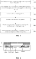
- FIG. 2 is a flowchart of a method for detecting a thickness of a protection layer of a fingerprint sensor according to an embodiment of the present invention.
- the method for detecting a thickness of a protection layer of a fingerprint sensor includes the following steps:
- step S100 referring to FIG. 3 , a signal scattering diagram of the fingerprint sensor is illustrated.
- the fingerprint sensor includes a plurality of chip sensing units (pixels), which are arranged in an array. Fingerprint texture depth data output by the chip sensing unit reflects fingerprint texture information.
- a press signal may be generated in a contact position between the fingerprint simulating device 31 and the fingerprint sensor, and then the press signal is received by the chip sensing unit arranged below the contact position. Since a covering layer and an adhesive are sandwiched between the fingerprint simulating device and the chip sensing unit, the press signal is scattered to the chip sensing unit in the manner as illustrated by an arrow 32 in FIG. 3 .
- FIG. 3 is a chip sensing unit that is directly pressed, and Pixel 6, Pixel 7 and Pixel 14 are chip sensing units that are not pressed by the fingerprint simulating device but may still receive the scattered signals from the oblique top portions.
- FIG. 4 is a schematic diagram illustrating strengths of output signals of all chip sensing units.
- FIG. 5 is a comparison diagram of strengths of output signals of chip sensing units having protection layers with different thicknesses. A greater thickness of the protection layer indicates a larger scattering range of the press signal and a smaller curve slope of the signal output by the chip sensing unit.
- the method for detecting a thickness of a protection layer of a fingerprint sensor according to the present invention implements thickness detection based on the above scattering feature of the press signal.
- the fingerprint simulating device may be a prosthetic finger including an object that has electrical features or is approximate to a finger, for example, a metal block, an electrically conductive rubber and the like. No special requirement is imposed on the specific texture of the prosthetic finger. However, textures of prosthetic fingers calculated by using the same calculation formula need to be identical.
- Step S200 Fingerprint data on a protection layer of the fingerprint simulating device is collected via the fingerprint sensor, and a frame of fingerprint data is acquired.
- D i,j denotes a derivative of a chip sensing unit in the i th row and j th column
- R i,j denotes fingerprint data of the chip sensing unit in the i th row and j th column.
- Q i,j denotes a normalization result of the derivative of the chip sensing unit in the i th row and j th column
- D max denotes a maximum derivative value of a current frame of fingerprint data
- D min denotes a minimum derivative value of the current frame of fingerprint data.
- I denotes an integration result
- row denotes a total number of rows of pixels
- col denotes a total number of columns of the pixels.
- Step S600 A thickness of a protection layer of the fingerprint sensor is calculated by introducing the integration result into a fitting formula.
- step S600 different fitting formulas may be used according to the specific relationships.
- T denotes a calculated thickness of the protection layer
- K and B denote fitting parameters.
- the fitting parameters are calculated by using such methods as the least square method and the like. Firstly, integration results I of a plurality of fingerprint sensors need to be collected and calculated through steps 200 to 500, then the thicknesses of the protection layers of these fingerprint sensors are calculated, and finally the fitting parameters K and B are calculated according to the integration results I and the thicknesses T of the protection layers.
- FIG. 6 is a schematic structural diagram of a system for detecting a thickness of a protection layer of a fingerprint sensor according to an embodiment of the present invention.
- the system for detecting a thickness of a protection layer of a fingerprint sensor includes: a fingerprint simulating device, a fingerprint collecting unit, a derivative calculating unit, a derivative normalizing unit, an integration calculating unit and a protection layer thickness calculating unit; wherein the fingerprint simulating device, the fingerprint collecting unit, the derivative calculating unit, the derivative normalizing unit, the integration calculating unit and the protection layer thickness calculating unit are sequentially connected.
- the fingerprint simulating device is configured to simulate a finger to press a protection layer of a fingerprint sensor.
- the fingerprint simulating device may be a prosthetic finger including an object that has electrical features or is approximate to a finger, for example, a metal block, an electrically conductive rubber and the like. No special requirement is imposed on the specific texture of the prosthetic finger. However, textures of prosthetic fingers calculated by using the same calculation formula need to be identical.
- the fingerprint collecting unit is configured to collect fingerprint data on the protection layer of the fingerprint simulating device, to acquire a frame of fingerprint data; wherein the fingerprint collecting unit is an array of chip sensing units.
- D i,j denotes a derivative of a chip sensing unit in the i th row and j th column
- R i,j denotes fingerprint data of the chip sensing unit in the i th row and j th column.
- Q i,j denotes a normalization result of the derivative of the chip sensing unit in the i th row and j th column
- D max denotes a maximum derivative value of a current frame of fingerprint data
- D min denotes a minimum derivative value of the current frame of fingerprint data.
- I denotes an integration result
- row denotes the total number of rows of pixels
- col denotes the total number of columns of the pixels.
- the protection layer thickness calculating unit is configured to calculate a thickness of a protection layer of the fingerprint sensor by introducing the integration result into a fitting formula; wherein different fitting formulas may be used according to the specific relationships.
- T denotes a calculated thickness of the protection layer
- K and B denote fitting parameters.
- the fitting parameters are calculated by using such methods as the least square method and the like. Firstly, integration results I of a plurality of fingerprint sensors need to be collected and calculated by sequentially using the fingerprint collecting unit, the derivative calculating unit, the derivative normalizing unit and the integration calculating unit, then the thicknesses of the protection layers of these fingerprint sensors are calculated, and finally the fitting parameters K and B are calculated according to the integration results I and the thicknesses T of the protection layers.
- the thickness of the protection layer of the fingerprint sensor is calculated according to the fingerprint data collected by the fingerprint sensor, and thus the thickness of the protection layer of the fingerprint sensor may be measured without damaging the fingerprint sensor. Moreover, measurement may be carried out for each sensor during mass production, and thus product quality may be better controlled and the measurement cost is low.
Landscapes
- Engineering & Computer Science (AREA)
- Physics & Mathematics (AREA)
- General Physics & Mathematics (AREA)
- Theoretical Computer Science (AREA)
- Life Sciences & Earth Sciences (AREA)
- Human Computer Interaction (AREA)
- Multimedia (AREA)
- Health & Medical Sciences (AREA)
- Surgery (AREA)
- Pathology (AREA)
- Biomedical Technology (AREA)
- Heart & Thoracic Surgery (AREA)
- Medical Informatics (AREA)
- Molecular Biology (AREA)
- Biophysics (AREA)
- Animal Behavior & Ethology (AREA)
- General Health & Medical Sciences (AREA)
- Public Health (AREA)
- Veterinary Medicine (AREA)
- Artificial Intelligence (AREA)
- Bioinformatics & Cheminformatics (AREA)
- Bioinformatics & Computational Biology (AREA)
- Computer Vision & Pattern Recognition (AREA)
- Data Mining & Analysis (AREA)
- Evolutionary Biology (AREA)
- Evolutionary Computation (AREA)
- General Engineering & Computer Science (AREA)
- Measurement Of Length, Angles, Or The Like Using Electric Or Magnetic Means (AREA)
- Image Input (AREA)
Abstract
Description
- The present invention relates to the technical field of fingerprint sensor detection, and in particular, relates to a method and a system for detecting a thickness of a protection layer of a fingerprint sensor.
- Fingerprints refer to textures formed by uneven skin surface of fingers. The fingerprint has unique and stable texture characteristics, and is generally used as a basis for identity recognition. A fingerprint sensor is a sensor for identity recognition by using the fingerprint.
-
FIG. 1 is a schematic structural diagram of a conventional fingerprint sensor. The fingerprint sensor includes acovering layer 11, an adhesive 12 and afingerprint sensor chip 13. The coveringlayer 11 may be made from glass, sapphire, coating or the like, and is mainly intended to protect thefingerprint sensor chip 13. Theadhesive 12 is adapted for fixing the coveringlayer 11 to the fingerprint sensor chip. Thefingerprint sensor chip 13 includes a matrix formed of thousands of pixels 14 (chip sensing units). When a finger presses the fingerprint sensor, thepixel 14 senses a fingerprint texture depth of the finger 15 thereon, and a matrix formed of fingerprint text depth data output by all thepixels 14 constitutes fingerprint texture information of the finger 15. - The protection layer (including the covering
layer 11 and the adhesive 12) of the fingerprint sensor is between the finger 15 and thefingerprint sensor chip 13. Therefore, the thickness of the protection layer may affect the signal-to-noise ratio of the fingerprint texture depth data collected by the fingerprint sensor, and accordingly directly affect the fingerprint texture depth data acquired by the fingerprint sensor. If the protection layer of the fingerprint sensor is too thick or too thin, performance of the product and user experience may all be directly impacted. Therefore, the thickness of the protection layer of the fingerprint needs to be strictly controlled. - Since a frame of the fingerprint sensor is generally wrapped by a protective or decorative material, the thickness of the protection layer may not be directly measured from a side of the fingerprint sensor. A conventional method for measuring the thickness of a protection layer is to directly cutting off the fingerprint sensor and then measuring the thickness of the protection layer by using a microscope. However, the method is defective in that the fingerprint sensor needs to be destroyed for the measurement; and therefore only sample detection may be carried out during mass production, measurement may not carried out for all the fingerprint sensors, and moreover, the measurement cost is high.
- The present invention provides a method and system for detecting a thickness of a protection layer of a fingerprint sensor, which are intended to solve the technical problems that in the convention method for detecting a thickness of a protection layer of a fingerprint sensor, sample detection may only be implemented, measurement may not carried out for all the fingerprint sensors, and the measurement cost is high.
- To solve the above technical problem, one technical solution employed by embodiments of the present invention is a method for detecting a thickness of a protection layer of a fingerprint sensor. The method includes the following steps:
- step a: collecting fingerprint data via a fingerprint sensor, the fingerprint sensor including a plurality of chip sensing units, being arranged in an array;
- step b: calculating a derivative of the fingerprint data, normalizing the derivative of the fingerprint data, and calculating an integration of the fingerprint data according to the normalized derivative of the fingerprint data; and
- step c: acquiring a thickness of a protection layer of the fingerprint sensor according to the integration of the fingerprint sensor.
- In this technical solution employed by embodiments of the present invention, step a further includes: pressing the fingerprint sensor by using a fingerprint simulating device; wherein the fingerprint simulating device is a prosthetic finger including an object that has electrical features or is approximate to a finger.
- In this technical solution employed by embodiments of the present invention, in step b, the derivative of the fingerprint data is calculated by using the following formula:

wherein Di,j denotes a derivative of a chip sensing unit in the ith row and jtn column, and Ri,j denotes fingerprint data of the chip sensing unit in the ith row and jtn column. - In this technical solution employed by embodiments of the present invention, in step b, the derivative of the fingerprint data is normalized by using the following formula:

wherein Qi,j denotes a normalization result of the derivative of the chip sensing unit in the ith row and jth column, Dmax denotes a maximum derivative value of a current frame of fingerprint data, and Dmin denotes a minimum derivative value of the current frame of fingerprint data. - In this technical solution employed by embodiments of the present invention, in step b, the integration of the fingerprint sensor is calculated by using the following formula:

wherein I denotes an integration result, row denotes a total number of rows of the chip sensing units, and col denotes a total number of columns of the chip sensing units. - In this technical solution employed by embodiments of the present invention, in step c, the thickness of the protection layer of the fingerprint sensor is calculated by using a linear fitting formula:

wherein T denotes a calculated thickness of the protection layer, and K and B denote fitting parameters. - Another technical solution employed by embodiments of the present invention is a system for detecting a thickness of a protection layer of a fingerprint sensor. The system includes: a fingerprint collecting unit, a derivative calculating unit, a derivative normalizing unit, an integration calculating unit and a protection layer thickness calculating unit; wherein the fingerprint collecting unit, the derivative calculating unit, the derivative normalizing unit, the integration calculating unit and the protection layer thickness calculating unit are sequentially connected;
the fingerprint collecting unit is configured to collect fingerprint data and includes a plurality of chip sensing units, arranged in an array;
the derivative calculating unit is configured to calculate a derivative of the fingerprint data;
the derivative normalizing unit is configured to normalize the derivative of the fingerprint data;
the integration calculating unit is configured to calculate an integration according to the normalized derivative of the fingerprint data; and
the protection layer thickness calculating unit is configured to calculate a thickness of the protection layer of the fingerprint sensor according to an integration result. - In this technical solution employed by embodiments of the present invention, the system further includes: a fingerprint simulating device, connected to the fingerprint collecting unit, the fingerprint simulating device is configured to simulate a finger to press the fingerprint sensor, and the fingerprint simulating device is a prosthetic finger including an object that has electrical features or is approximate to a finger.
- In this technical solution employed by embodiments of the present invention, the derivative calculating unit calculates the derivative of the fingerprint data by using the following formula:

wherein Di,j denotes a derivative of a chip sensing unit in the ith row and jtn column, and Ri,j denotes fingerprint data of the chip sensing unit in the ith row and jtn column; and - the derivative normalizing unit normalizes the derivative of the fingerprint data by using the following formula:

wherein Qi,j denotes a normalization result of the derivative of the chip sensing unit in the ith row and jth column, Dmax denotes a maximum derivative value of a current frame of fingerprint data, and Dmin denotes a minimum derivative value of the current frame of fingerprint data. - In this technical solution employed by embodiments of the present invention, the integration calculating unit calculates the integration of the fingerprint sensor by using the following formula:

wherein I denotes an integration result, row denotes the total number of rows of the chip sensing units, and col denotes the total number of columns of the chip sensing units; - the protection layer thickness calculating unit calculates the thickness of the protection layer of the sensor by using a linear fitting formula:

wherein T denotes a calculated thickness of the protection layer, and K and B denote fitting parameters. - As compared with the prior art, the present invention has the following beneficial effects: In the method and system for detecting a thickness of a protection layer of a fingerprint sensor according to the embodiments of the present invention, the thickness of the protection layer of the fingerprint sensor is calculated according to the fingerprint data acquired by the fingerprint sensor, and thus the thickness of the protection layer of the fingerprint sensor may be measured without causing damages to the fingerprint sensor; during mass production, measurement may be carried out for each sensor, and thus product quality may be better controlled; and the measurement cost is low.
-
-
FIG. 1 is a schematic structural diagram of a conventional fingerprint sensor; -
FIG. 2 is a flowchart of a method for detecting a thickness of a protection layer of a fingerprint sensor according to an embodiment of the present invention; -
FIG. 3 is a diagram illustrating signal scattering of a fingerprint sensor; -
FIG. 4 is a schematic diagram illustrating strength of an output signal of a chip sensing unit; -
FIG. 5 is a comparison diagram of strengths of output signals of chip sensing units having protection layers with different thicknesses; and -
FIG. 6 is a schematic structural diagram of a system for detecting a thickness of a protection layer of a fingerprint sensor according to an embodiment of the present invention. - For better understanding of the present invention, the present invention is thoroughly described with reference to relevant accompanying drawings. The accompanying drawings show preferential embodiments of the present invention. However, the present invention may be implemented in a plurality of forms or ways, and is not limited to the embodiments described herein. On the contrary, the embodiments described herein are intended to make the disclosure of the present invention more clearly and thoroughly understood.
- Unless otherwise defined, all the technical and scientific terms used in this specification convey the same meanings as the meanings commonly understood by a person skilled in the art. Additionally, the terms used in the specification the present invention are merely for describing the objective of the specific embodiments, and are not intended to limit the present invention.
-
FIG. 2 is a flowchart of a method for detecting a thickness of a protection layer of a fingerprint sensor according to an embodiment of the present invention. The method for detecting a thickness of a protection layer of a fingerprint sensor includes the following steps: - Step S100: A fingerprint simulating device having specific texture is pressed on a protection layer of a fingerprint sensor.
- In step S100, referring to
FIG. 3 , a signal scattering diagram of the fingerprint sensor is illustrated. The fingerprint sensor includes a plurality of chip sensing units (pixels), which are arranged in an array. Fingerprint texture depth data output by the chip sensing unit reflects fingerprint texture information. When afingerprint simulating device 31 presses the fingerprint sensor, a press signal may be generated in a contact position between thefingerprint simulating device 31 and the fingerprint sensor, and then the press signal is received by the chip sensing unit arranged below the contact position. Since a covering layer and an adhesive are sandwiched between the fingerprint simulating device and the chip sensing unit, the press signal is scattered to the chip sensing unit in the manner as illustrated by anarrow 32 inFIG. 3 . Although right top portions of some chip sensing units are not pressed by the fingerprint simulating device, these chip sensing units may still receive the press signal of the fingerprint simulating device scattered from oblique top portions thereof. Therefore, these chip sensing units still output signals which are less than signals output by the chip sensing units that are directly pressed at the right top portions thereof. As illustrated inFIG. 3 , Pixel 2 is a chip sensing unit that is directly pressed, and Pixel 6, Pixel 7 andPixel 14 are chip sensing units that are not pressed by the fingerprint simulating device but may still receive the scattered signals from the oblique top portions. Such a chip sensing unit as Pixel 10 that is neither directly pressed nor receives any scattered signal output no signal (which outputs noise only). Specifically,FIG. 4 is a schematic diagram illustrating strengths of output signals of all chip sensing units. - Experiments find that the range and strength of scattering of the press signal of the fingerprint simulating device is relevant to the thickness of the protection layer.
FIG. 5 is a comparison diagram of strengths of output signals of chip sensing units having protection layers with different thicknesses. A greater thickness of the protection layer indicates a larger scattering range of the press signal and a smaller curve slope of the signal output by the chip sensing unit. The method for detecting a thickness of a protection layer of a fingerprint sensor according to the present invention implements thickness detection based on the above scattering feature of the press signal. In the embodiment of the present invention, the fingerprint simulating device may be a prosthetic finger including an object that has electrical features or is approximate to a finger, for example, a metal block, an electrically conductive rubber and the like. No special requirement is imposed on the specific texture of the prosthetic finger. However, textures of prosthetic fingers calculated by using the same calculation formula need to be identical. - Step S200: Fingerprint data on a protection layer of the fingerprint simulating device is collected via the fingerprint sensor, and a frame of fingerprint data is acquired.
- Step S300: A derivative of the fingerprint data is calculated, wherein the derivative of the fingerprint data is calculated by using the following formula:

- In formula (1), Di,j denotes a derivative of a chip sensing unit in the ith row and jth column, and Ri,j denotes fingerprint data of the chip sensing unit in the ith row and jth column.
- Step S400: The derivative of the fingerprint data is normalized, wherein the derivative of the fingerprint data is normalized by using the following formula:

- In formula (2), Qi,j denotes a normalization result of the derivative of the chip sensing unit in the ith row and jth column, Dmax denotes a maximum derivative value of a current frame of fingerprint data, and Dmin denotes a minimum derivative value of the current frame of fingerprint data.
- Step S500: An integration of the fingerprint sensor is calculated according to the normalized derivative of the fingerprint data, wherein the integration of the fingerprint sensor is calculated by using the following formula:

- In formula (3), I denotes an integration result, row denotes a total number of rows of pixels, and col denotes a total number of columns of the pixels.
- Step S600: A thickness of a protection layer of the fingerprint sensor is calculated by introducing the integration result into a fitting formula.
- In step S600, different fitting formulas may be used according to the specific relationships. In the embodiment of the present invention, the thickness of the protection layer is calculated a linear fitting formula:

- In formula (4), T denotes a calculated thickness of the protection layer, and K and B denote fitting parameters. The fitting parameters are calculated by using such methods as the least square method and the like. Firstly, integration results I of a plurality of fingerprint sensors need to be collected and calculated through steps 200 to 500, then the thicknesses of the protection layers of these fingerprint sensors are calculated, and finally the fitting parameters K and B are calculated according to the integration results I and the thicknesses T of the protection layers.
-
FIG. 6 is a schematic structural diagram of a system for detecting a thickness of a protection layer of a fingerprint sensor according to an embodiment of the present invention. The system for detecting a thickness of a protection layer of a fingerprint sensor includes: a fingerprint simulating device, a fingerprint collecting unit, a derivative calculating unit, a derivative normalizing unit, an integration calculating unit and a protection layer thickness calculating unit; wherein the fingerprint simulating device, the fingerprint collecting unit, the derivative calculating unit, the derivative normalizing unit, the integration calculating unit and the protection layer thickness calculating unit are sequentially connected. - The fingerprint simulating device is configured to simulate a finger to press a protection layer of a fingerprint sensor.
- In the embodiment of the present invention, the fingerprint simulating device may be a prosthetic finger including an object that has electrical features or is approximate to a finger, for example, a metal block, an electrically conductive rubber and the like. No special requirement is imposed on the specific texture of the prosthetic finger. However, textures of prosthetic fingers calculated by using the same calculation formula need to be identical.
- The fingerprint collecting unit is configured to collect fingerprint data on the protection layer of the fingerprint simulating device, to acquire a frame of fingerprint data; wherein the fingerprint collecting unit is an array of chip sensing units.
- The derivative calculating unit is configured to calculate a derivative of the fingerprint data, wherein the derivative of the fingerprint data is calculated by using the following formula:

- In formula (1), Di,j denotes a derivative of a chip sensing unit in the ith row and jth column, and Ri,j denotes fingerprint data of the chip sensing unit in the ith row and jth column.
- The derivative normalizing unit is configured to normalize the derivative of the fingerprint data, wherein the derivative of the fingerprint data is normalized by using the following formula:

- In formula (2), Qi,j denotes a normalization result of the derivative of the chip sensing unit in the ith row and jth column, Dmax denotes a maximum derivative value of a current frame of fingerprint data, and Dmin denotes a minimum derivative value of the current frame of fingerprint data.
- The integration calculating unit is configured to calculate an integration of the fingerprint sensor according to the normalized derivative of the fingerprint data, wherein the integration of the fingerprint sensor is calculated by using the following formula:

- In formula (3), I denotes an integration result, row denotes the total number of rows of pixels, and col denotes the total number of columns of the pixels.
- The protection layer thickness calculating unit is configured to calculate a thickness of a protection layer of the fingerprint sensor by introducing the integration result into a fitting formula; wherein different fitting formulas may be used according to the specific relationships. In the embodiment of the present invention, the thickness of the protection layer is calculated a linear fitting formula:

- In formula (4), T denotes a calculated thickness of the protection layer, and K and B denote fitting parameters. The fitting parameters are calculated by using such methods as the least square method and the like. Firstly, integration results I of a plurality of fingerprint sensors need to be collected and calculated by sequentially using the fingerprint collecting unit, the derivative calculating unit, the derivative normalizing unit and the integration calculating unit, then the thicknesses of the protection layers of these fingerprint sensors are calculated, and finally the fitting parameters K and B are calculated according to the integration results I and the thicknesses T of the protection layers.
- In the method and system for detecting a thickness of a protection layer of a fingerprint sensor according to the embodiments of the present invention, the thickness of the protection layer of the fingerprint sensor is calculated according to the fingerprint data collected by the fingerprint sensor, and thus the thickness of the protection layer of the fingerprint sensor may be measured without damaging the fingerprint sensor. Moreover, measurement may be carried out for each sensor during mass production, and thus product quality may be better controlled and the measurement cost is low.
- Described above are preferred embodiments of the present invention. However, implementation of the present invention is not limited to the above embodiments. Any variations, polishments, substitutions, combinations, or simplifications, or the like equivalent replacements made to the present invention without departing from the spiritual essence and principle of the present invention shall all be covered within the protection scope of the present invention.
Claims (10)
- A method for detecting a thickness of a protection layer of a fingerprint sensor, the method comprising:step a: collecting fingerprint data via a fingerprint sensor, the fingerprint sensor comprising a plurality of chip sensing units arranged in an array;step b: calculating a derivative of the fingerprint data, normalizing the derivative of the fingerprint data, and calculating an integration according to the normalized derivative of the fingerprint data; andstep c: acquiring a thickness of a protection layer of the fingerprint sensor according to the integration result.
- The method for detecting a thickness of a protection layer of a fingerprint sensor according to claim 1, wherein step a further comprises:pressing the fingerprint sensor by using a fingerprint simulating device, wherein the fingerprint simulating device is a prosthetic finger comprising an object that has electrical features or is approximate to a finger.
- The method for detecting a thickness of a protection layer of a fingerprint sensor according to claim 1 or 2, wherein in step b, the derivative of the fingerprint data is calculated by using the following formula:

- The method for detecting a thickness of a protection layer of a fingerprint sensor according to claim 3, wherein in step b, the derivative of the fingerprint data is normalized by using the following formula:

- The method for detecting a thickness of a protection layer of a fingerprint sensor according to claim 4, wherein in step b, the integration is calculated by using the following formula:

- The method for detecting a thickness of a protection layer of a fingerprint sensor according to claim 4, wherein in step c, the thickness of the protection layer of the fingerprint sensor is calculated by using a linear fitting formula:

- A system for detecting a thickness of a protection layer of a fingerprint sensor, comprising: a fingerprint collecting unit, a derivative calculating unit, a derivative normalizing unit, an integration calculating unit and a protection layer thickness calculating unit; wherein the fingerprint collecting unit, the derivative calculating unit, the derivative normalizing unit, the integration calculating unit and the protection layer thickness calculating unit are sequentially connected;
the fingerprint collecting unit is configured to collect fingerprint data and comprises a plurality of chip sensing units arranged in an array;
the derivative calculating unit is configured to calculate a derivative of the fingerprint data;
the derivative normalizing unit is configured to normalize the derivative of the fingerprint data;
the integration calculating unit is configured to calculate an integration according to the normalized derivative of the fingerprint data; and
the protection layer thickness calculating unit is configured to calculate a thickness of the protection layer of the fingerprint sensor according to an integration result. - The system for detecting a thickness of a protection layer of a fingerprint sensor according to claim 7, further comprising a fingerprint simulating device connected to the fingerprint collecting unit, the fingerprint simulating device is configured to simulate a finger to press the fingerprint sensor, and the fingerprint simulating device is a prosthetic finger comprising an object that has electrical features or is approximate to a finger.
- The system for detecting a thickness of a protection layer of a fingerprint sensor according to claim 7 or 8, wherein the derivative calculating unit calculates the derivative of the fingerprint data by using the following formula:


- The system for detecting a thickness of a protection layer of a fingerprint sensor according to claim 9, wherein the integration calculating unit calculates the integration of the fingerprint sensor by using the following formula:

the protection layer thickness calculating unit calculates the thickness of the protection layer of the sensor by calculating the thickness of the protection layer using a linear fitting formula:
Applications Claiming Priority (2)
| Application Number | Priority Date | Filing Date | Title |
|---|---|---|---|
| CN201510956858.XA CN106767628B (en) | 2015-12-18 | 2015-12-18 | A kind of thickness detecting method and system of fingerprint sensor protective layer |
| PCT/CN2016/091673 WO2017101448A1 (en) | 2015-12-18 | 2016-07-26 | Method and system for detecting fingerprint sensor protection layer thickness |
Publications (3)
| Publication Number | Publication Date |
|---|---|
| EP3249346A1 true EP3249346A1 (en) | 2017-11-29 |
| EP3249346A4 EP3249346A4 (en) | 2018-04-11 |
| EP3249346B1 EP3249346B1 (en) | 2019-07-17 |
Family
ID=58965306
Family Applications (1)
| Application Number | Title | Priority Date | Filing Date |
|---|---|---|---|
| EP16874509.9A Active EP3249346B1 (en) | 2015-12-18 | 2016-07-26 | Method and system for detecting fingerprint sensor protection layer thickness |
Country Status (5)
| Country | Link |
|---|---|
| US (1) | US10739134B2 (en) |
| EP (1) | EP3249346B1 (en) |
| KR (1) | KR101939523B1 (en) |
| CN (1) | CN106767628B (en) |
| WO (1) | WO2017101448A1 (en) |
Families Citing this family (5)
| Publication number | Priority date | Publication date | Assignee | Title |
|---|---|---|---|---|
| KR102544608B1 (en) * | 2018-07-04 | 2023-06-19 | 삼성전자주식회사 | Method for operating authorization related the biometric information, based on an image including the biometric information obtained by using the biometric sensor and the electronic device supporting the same |
| TWM606450U (en) * | 2019-11-12 | 2021-01-11 | 神盾股份有限公司 | Ultrasonic fingerprint sensor |
| KR102960576B1 (en) * | 2019-11-20 | 2026-05-04 | 삼성전자주식회사 | Electronic device and method for recognizing fingerprint thereof |
| CN115131839B (en) * | 2021-03-26 | 2026-01-09 | 北京小米移动软件有限公司 | Fingerprint model construction methods, devices, electronic equipment and storage media |
| WO2024039136A1 (en) | 2022-08-17 | 2024-02-22 | 삼성전자 주식회사 | Method for adjusting configuration data of fingerprint sensor, and electronic device |
Family Cites Families (18)
| Publication number | Priority date | Publication date | Assignee | Title |
|---|---|---|---|---|
| US6088471A (en) * | 1997-05-16 | 2000-07-11 | Authentec, Inc. | Fingerprint sensor including an anisotropic dielectric coating and associated methods |
| JP4612958B2 (en) * | 2001-02-01 | 2011-01-12 | グンゼ株式会社 | Shape transfer film |
| US6693441B2 (en) * | 2001-11-30 | 2004-02-17 | Stmicroelectronics, Inc. | Capacitive fingerprint sensor with protective coating containing a conductive suspension |
| JP3766034B2 (en) * | 2002-02-20 | 2006-04-12 | 富士通株式会社 | Fingerprint sensor device and manufacturing method thereof |
| JP2004310577A (en) * | 2003-04-09 | 2004-11-04 | Matsushita Electric Ind Co Ltd | Uneven pattern detection device and portable device |
| US7420163B2 (en) * | 2005-04-29 | 2008-09-02 | Revera Incorporated | Determining layer thickness using photoelectron spectroscopy |
| CN101403604A (en) * | 2008-10-22 | 2009-04-08 | 中国科学院上海技术物理研究所 | Extension thin film surface protection test technology |
| US20120092324A1 (en) * | 2010-10-18 | 2012-04-19 | Qualcomm Mems Technologies, Inc. | Touch, handwriting and fingerprint sensor with elastomeric spacer layer |
| SG188414A1 (en) * | 2010-11-12 | 2013-04-30 | Ev Group E Thallner Gmbh | Measurement means and method for measuring layer thicknesses and voids of a wafer stack |
| CN102564326A (en) * | 2010-12-28 | 2012-07-11 | 中国航空工业标准件制造有限责任公司 | Measuring method for thickness of extremely thin covering layer |
| CN102313521A (en) * | 2011-03-29 | 2012-01-11 | 上海华碧检测技术有限公司 | Method for measuring thickness of organic protective film |
| CN103206914A (en) * | 2013-03-27 | 2013-07-17 | 苏州江南航天机电工业有限公司 | Device for detecting thickness of pouring coverage layer |
| US10203816B2 (en) * | 2013-05-07 | 2019-02-12 | Egis Technology Inc. | Apparatus and method for TFT fingerprint sensor |
| CN203642899U (en) * | 2013-10-29 | 2014-06-11 | 中芯国际集成电路制造(北京)有限公司 | Copper film thickness measurement standard sheet |
| KR101621286B1 (en) * | 2014-05-16 | 2016-05-16 | 크루셜텍 (주) | Method of manufacturing fingerprint sensor module |
| CN104102902B (en) * | 2014-07-04 | 2017-07-04 | 京东方科技集团股份有限公司 | A kind of semiconductor fingerprint identification sensor and its manufacture method |
| CN107358188B (en) * | 2015-01-13 | 2021-12-07 | 深圳市汇顶科技股份有限公司 | Fingerprint sensor and correction method thereof |
| US9811711B2 (en) * | 2015-02-22 | 2017-11-07 | Microsoft Technology Licensing, Llc | Fingerprint detection with transparent cover |
-
2015
- 2015-12-18 CN CN201510956858.XA patent/CN106767628B/en active Active
-
2016
- 2016-07-26 WO PCT/CN2016/091673 patent/WO2017101448A1/en not_active Ceased
- 2016-07-26 EP EP16874509.9A patent/EP3249346B1/en active Active
- 2016-07-26 KR KR1020177022870A patent/KR101939523B1/en active Active
-
2017
- 2017-08-14 US US15/676,205 patent/US10739134B2/en active Active
Also Published As
| Publication number | Publication date |
|---|---|
| CN106767628B (en) | 2019-04-19 |
| US10739134B2 (en) | 2020-08-11 |
| US20170343341A1 (en) | 2017-11-30 |
| KR20170102558A (en) | 2017-09-11 |
| WO2017101448A1 (en) | 2017-06-22 |
| CN106767628A (en) | 2017-05-31 |
| EP3249346A4 (en) | 2018-04-11 |
| KR101939523B1 (en) | 2019-01-16 |
| EP3249346B1 (en) | 2019-07-17 |
Similar Documents
| Publication | Publication Date | Title |
|---|---|---|
| US10739134B2 (en) | Method and system for detecting fingerprint sensor protection layer thickness | |
| US11055506B2 (en) | Method of analyzing a fingerprint | |
| US7848798B2 (en) | Live finger detection by four-point measurement of complex impedance | |
| AU785138B2 (en) | Environmental noise monitoring | |
| JP2002162204A (en) | Resistive finger detection for fingerprint sensor | |
| US9182319B2 (en) | Automatic detection and analysis of tire treads | |
| US10884563B2 (en) | Method for determining change of initial distance of sensing electrode | |
| KR950006966A (en) | Nondestructive Measurement of Plasma Processing Characteristics | |
| CN106908517A (en) | A kind of damage reason location imaging method of the passive monitoring information fusion of Lamb wave master | |
| KR102881015B1 (en) | Electronic apparatus and method for processing fingerprint image thereof | |
| CN115406860B (en) | A rapid detection device and method for Huanglongbing based on modeling comparison | |
| US20130214801A1 (en) | Pressure-based Fingerprint Authentication Device | |
| CN101621710B (en) | Method and system for evaluating video quality based on edge detection | |
| CN115512097A (en) | Method for digitally processing multiple pixels and temperature measuring device | |
| JP2009223462A (en) | Personal identification device and personal identification method | |
| KR101492254B1 (en) | Ultrasound diagnostic apparatus and method for quality control | |
| CN103471811A (en) | Method for measuring detective quantum efficiency and system thereof | |
| CN112053299A (en) | Image processing method based on colloidal gold immunochromatography | |
| EP0923341B1 (en) | Process and system for identification of persons | |
| EP2867748B1 (en) | Method for determining whether at least one key of a device having multiple keys has been actuated | |
| US12632149B1 (en) | Ultrasonic fingerprint sensor configuration based on A-line data | |
| Mammadova et al. | Towards melanoma detection using radar and image data | |
| CN106580316A (en) | Device for assessing brain neurotransmitter activities and assessment method of device | |
| JP2000005147A (en) | Personal authentication device | |
| CN120778857A (en) | Real-time mass spectrometry system for detecting volatile gas components of grains |
Legal Events
| Date | Code | Title | Description |
|---|---|---|---|
| STAA | Information on the status of an ep patent application or granted ep patent |
Free format text: STATUS: THE INTERNATIONAL PUBLICATION HAS BEEN MADE |
|
| PUAI | Public reference made under article 153(3) epc to a published international application that has entered the european phase |
Free format text: ORIGINAL CODE: 0009012 |
|
| STAA | Information on the status of an ep patent application or granted ep patent |
Free format text: STATUS: REQUEST FOR EXAMINATION WAS MADE |
|
| 17P | Request for examination filed |
Effective date: 20170821 |
|
| AK | Designated contracting states |
Kind code of ref document: A1 Designated state(s): AL AT BE BG CH CY CZ DE DK EE ES FI FR GB GR HR HU IE IS IT LI LT LU LV MC MK MT NL NO PL PT RO RS SE SI SK SM TR |
|
| AX | Request for extension of the european patent |
Extension state: BA ME |
|
| REG | Reference to a national code |
Ref country code: DE Ref legal event code: R079 Ref document number: 602016017142 Country of ref document: DE Free format text: PREVIOUS MAIN CLASS: G01B0007060000 Ipc: G01B0021080000 |
|
| A4 | Supplementary search report drawn up and despatched |
Effective date: 20180312 |
|
| RIC1 | Information provided on ipc code assigned before grant |
Ipc: G06K 9/00 20060101ALI20180306BHEP Ipc: G01B 21/08 20060101AFI20180306BHEP Ipc: G01B 7/06 20060101ALI20180306BHEP Ipc: A61B 5/117 20160101ALI20180306BHEP |
|
| DAV | Request for validation of the european patent (deleted) | ||
| DAX | Request for extension of the european patent (deleted) | ||
| GRAP | Despatch of communication of intention to grant a patent |
Free format text: ORIGINAL CODE: EPIDOSNIGR1 |
|
| STAA | Information on the status of an ep patent application or granted ep patent |
Free format text: STATUS: GRANT OF PATENT IS INTENDED |
|
| INTG | Intention to grant announced |
Effective date: 20190403 |
|
| GRAS | Grant fee paid |
Free format text: ORIGINAL CODE: EPIDOSNIGR3 |
|
| GRAA | (expected) grant |
Free format text: ORIGINAL CODE: 0009210 |
|
| STAA | Information on the status of an ep patent application or granted ep patent |
Free format text: STATUS: THE PATENT HAS BEEN GRANTED |
|
| AK | Designated contracting states |
Kind code of ref document: B1 Designated state(s): AL AT BE BG CH CY CZ DE DK EE ES FI FR GB GR HR HU IE IS IT LI LT LU LV MC MK MT NL NO PL PT RO RS SE SI SK SM TR |
|
| REG | Reference to a national code |
Ref country code: GB Ref legal event code: FG4D |
|
| REG | Reference to a national code |
Ref country code: CH Ref legal event code: EP |
|
| REG | Reference to a national code |
Ref country code: IE Ref legal event code: FG4D |
|
| REG | Reference to a national code |
Ref country code: DE Ref legal event code: R096 Ref document number: 602016017142 Country of ref document: DE |
|
| REG | Reference to a national code |
Ref country code: AT Ref legal event code: REF Ref document number: 1156264 Country of ref document: AT Kind code of ref document: T Effective date: 20190815 |
|
| REG | Reference to a national code |
Ref country code: NL Ref legal event code: MP Effective date: 20190717 |
|
| REG | Reference to a national code |
Ref country code: LT Ref legal event code: MG4D |
|
| REG | Reference to a national code |
Ref country code: AT Ref legal event code: MK05 Ref document number: 1156264 Country of ref document: AT Kind code of ref document: T Effective date: 20190717 |
|
| PG25 | Lapsed in a contracting state [announced via postgrant information from national office to epo] |
Ref country code: LT Free format text: LAPSE BECAUSE OF FAILURE TO SUBMIT A TRANSLATION OF THE DESCRIPTION OR TO PAY THE FEE WITHIN THE PRESCRIBED TIME-LIMIT Effective date: 20190717 Ref country code: HR Free format text: LAPSE BECAUSE OF FAILURE TO SUBMIT A TRANSLATION OF THE DESCRIPTION OR TO PAY THE FEE WITHIN THE PRESCRIBED TIME-LIMIT Effective date: 20190717 Ref country code: AT Free format text: LAPSE BECAUSE OF FAILURE TO SUBMIT A TRANSLATION OF THE DESCRIPTION OR TO PAY THE FEE WITHIN THE PRESCRIBED TIME-LIMIT Effective date: 20190717 Ref country code: BG Free format text: LAPSE BECAUSE OF FAILURE TO SUBMIT A TRANSLATION OF THE DESCRIPTION OR TO PAY THE FEE WITHIN THE PRESCRIBED TIME-LIMIT Effective date: 20191017 Ref country code: NL Free format text: LAPSE BECAUSE OF FAILURE TO SUBMIT A TRANSLATION OF THE DESCRIPTION OR TO PAY THE FEE WITHIN THE PRESCRIBED TIME-LIMIT Effective date: 20190717 Ref country code: PT Free format text: LAPSE BECAUSE OF FAILURE TO SUBMIT A TRANSLATION OF THE DESCRIPTION OR TO PAY THE FEE WITHIN THE PRESCRIBED TIME-LIMIT Effective date: 20191118 Ref country code: NO Free format text: LAPSE BECAUSE OF FAILURE TO SUBMIT A TRANSLATION OF THE DESCRIPTION OR TO PAY THE FEE WITHIN THE PRESCRIBED TIME-LIMIT Effective date: 20191017 Ref country code: SE Free format text: LAPSE BECAUSE OF FAILURE TO SUBMIT A TRANSLATION OF THE DESCRIPTION OR TO PAY THE FEE WITHIN THE PRESCRIBED TIME-LIMIT Effective date: 20190717 Ref country code: FI Free format text: LAPSE BECAUSE OF FAILURE TO SUBMIT A TRANSLATION OF THE DESCRIPTION OR TO PAY THE FEE WITHIN THE PRESCRIBED TIME-LIMIT Effective date: 20190717 |
|
| PG25 | Lapsed in a contracting state [announced via postgrant information from national office to epo] |
Ref country code: RS Free format text: LAPSE BECAUSE OF FAILURE TO SUBMIT A TRANSLATION OF THE DESCRIPTION OR TO PAY THE FEE WITHIN THE PRESCRIBED TIME-LIMIT Effective date: 20190717 Ref country code: GR Free format text: LAPSE BECAUSE OF FAILURE TO SUBMIT A TRANSLATION OF THE DESCRIPTION OR TO PAY THE FEE WITHIN THE PRESCRIBED TIME-LIMIT Effective date: 20191018 Ref country code: IS Free format text: LAPSE BECAUSE OF FAILURE TO SUBMIT A TRANSLATION OF THE DESCRIPTION OR TO PAY THE FEE WITHIN THE PRESCRIBED TIME-LIMIT Effective date: 20191117 Ref country code: AL Free format text: LAPSE BECAUSE OF FAILURE TO SUBMIT A TRANSLATION OF THE DESCRIPTION OR TO PAY THE FEE WITHIN THE PRESCRIBED TIME-LIMIT Effective date: 20190717 Ref country code: ES Free format text: LAPSE BECAUSE OF FAILURE TO SUBMIT A TRANSLATION OF THE DESCRIPTION OR TO PAY THE FEE WITHIN THE PRESCRIBED TIME-LIMIT Effective date: 20190717 Ref country code: LV Free format text: LAPSE BECAUSE OF FAILURE TO SUBMIT A TRANSLATION OF THE DESCRIPTION OR TO PAY THE FEE WITHIN THE PRESCRIBED TIME-LIMIT Effective date: 20190717 |
|
| REG | Reference to a national code |
Ref country code: CH Ref legal event code: PL |
|
| PG25 | Lapsed in a contracting state [announced via postgrant information from national office to epo] |
Ref country code: TR Free format text: LAPSE BECAUSE OF FAILURE TO SUBMIT A TRANSLATION OF THE DESCRIPTION OR TO PAY THE FEE WITHIN THE PRESCRIBED TIME-LIMIT Effective date: 20190717 |
|
| REG | Reference to a national code |
Ref country code: BE Ref legal event code: MM Effective date: 20190731 |
|
| PG25 | Lapsed in a contracting state [announced via postgrant information from national office to epo] |
Ref country code: PL Free format text: LAPSE BECAUSE OF FAILURE TO SUBMIT A TRANSLATION OF THE DESCRIPTION OR TO PAY THE FEE WITHIN THE PRESCRIBED TIME-LIMIT Effective date: 20190717 Ref country code: EE Free format text: LAPSE BECAUSE OF FAILURE TO SUBMIT A TRANSLATION OF THE DESCRIPTION OR TO PAY THE FEE WITHIN THE PRESCRIBED TIME-LIMIT Effective date: 20190717 Ref country code: IT Free format text: LAPSE BECAUSE OF FAILURE TO SUBMIT A TRANSLATION OF THE DESCRIPTION OR TO PAY THE FEE WITHIN THE PRESCRIBED TIME-LIMIT Effective date: 20190717 Ref country code: DK Free format text: LAPSE BECAUSE OF FAILURE TO SUBMIT A TRANSLATION OF THE DESCRIPTION OR TO PAY THE FEE WITHIN THE PRESCRIBED TIME-LIMIT Effective date: 20190717 Ref country code: RO Free format text: LAPSE BECAUSE OF FAILURE TO SUBMIT A TRANSLATION OF THE DESCRIPTION OR TO PAY THE FEE WITHIN THE PRESCRIBED TIME-LIMIT Effective date: 20190717 |
|
| PG25 | Lapsed in a contracting state [announced via postgrant information from national office to epo] |
Ref country code: SM Free format text: LAPSE BECAUSE OF FAILURE TO SUBMIT A TRANSLATION OF THE DESCRIPTION OR TO PAY THE FEE WITHIN THE PRESCRIBED TIME-LIMIT Effective date: 20190717 Ref country code: LI Free format text: LAPSE BECAUSE OF NON-PAYMENT OF DUE FEES Effective date: 20190731 Ref country code: SK Free format text: LAPSE BECAUSE OF FAILURE TO SUBMIT A TRANSLATION OF THE DESCRIPTION OR TO PAY THE FEE WITHIN THE PRESCRIBED TIME-LIMIT Effective date: 20190717 Ref country code: CH Free format text: LAPSE BECAUSE OF NON-PAYMENT OF DUE FEES Effective date: 20190731 Ref country code: MC Free format text: LAPSE BECAUSE OF FAILURE TO SUBMIT A TRANSLATION OF THE DESCRIPTION OR TO PAY THE FEE WITHIN THE PRESCRIBED TIME-LIMIT Effective date: 20190717 Ref country code: CZ Free format text: LAPSE BECAUSE OF FAILURE TO SUBMIT A TRANSLATION OF THE DESCRIPTION OR TO PAY THE FEE WITHIN THE PRESCRIBED TIME-LIMIT Effective date: 20190717 Ref country code: BE Free format text: LAPSE BECAUSE OF NON-PAYMENT OF DUE FEES Effective date: 20190731 Ref country code: LU Free format text: LAPSE BECAUSE OF NON-PAYMENT OF DUE FEES Effective date: 20190726 Ref country code: IS Free format text: LAPSE BECAUSE OF FAILURE TO SUBMIT A TRANSLATION OF THE DESCRIPTION OR TO PAY THE FEE WITHIN THE PRESCRIBED TIME-LIMIT Effective date: 20200224 |
|
| REG | Reference to a national code |
Ref country code: DE Ref legal event code: R097 Ref document number: 602016017142 Country of ref document: DE |
|
| PLBE | No opposition filed within time limit |
Free format text: ORIGINAL CODE: 0009261 |
|
| STAA | Information on the status of an ep patent application or granted ep patent |
Free format text: STATUS: NO OPPOSITION FILED WITHIN TIME LIMIT |
|
| PG2D | Information on lapse in contracting state deleted |
Ref country code: IS |
|
| PG25 | Lapsed in a contracting state [announced via postgrant information from national office to epo] |
Ref country code: IE Free format text: LAPSE BECAUSE OF NON-PAYMENT OF DUE FEES Effective date: 20190726 |
|
| 26N | No opposition filed |
Effective date: 20200603 |
|
| PG25 | Lapsed in a contracting state [announced via postgrant information from national office to epo] |
Ref country code: SI Free format text: LAPSE BECAUSE OF FAILURE TO SUBMIT A TRANSLATION OF THE DESCRIPTION OR TO PAY THE FEE WITHIN THE PRESCRIBED TIME-LIMIT Effective date: 20190717 |
|
| PG25 | Lapsed in a contracting state [announced via postgrant information from national office to epo] |
Ref country code: FR Free format text: LAPSE BECAUSE OF NON-PAYMENT OF DUE FEES Effective date: 20190917 |
|
| PG25 | Lapsed in a contracting state [announced via postgrant information from national office to epo] |
Ref country code: CY Free format text: LAPSE BECAUSE OF FAILURE TO SUBMIT A TRANSLATION OF THE DESCRIPTION OR TO PAY THE FEE WITHIN THE PRESCRIBED TIME-LIMIT Effective date: 20190717 |
|
| PG25 | Lapsed in a contracting state [announced via postgrant information from national office to epo] |
Ref country code: MT Free format text: LAPSE BECAUSE OF FAILURE TO SUBMIT A TRANSLATION OF THE DESCRIPTION OR TO PAY THE FEE WITHIN THE PRESCRIBED TIME-LIMIT Effective date: 20190717 Ref country code: HU Free format text: LAPSE BECAUSE OF FAILURE TO SUBMIT A TRANSLATION OF THE DESCRIPTION OR TO PAY THE FEE WITHIN THE PRESCRIBED TIME-LIMIT; INVALID AB INITIO Effective date: 20160726 |
|
| PG25 | Lapsed in a contracting state [announced via postgrant information from national office to epo] |
Ref country code: MK Free format text: LAPSE BECAUSE OF FAILURE TO SUBMIT A TRANSLATION OF THE DESCRIPTION OR TO PAY THE FEE WITHIN THE PRESCRIBED TIME-LIMIT Effective date: 20190717 |
|
| PGFP | Annual fee paid to national office [announced via postgrant information from national office to epo] |
Ref country code: DE Payment date: 20250708 Year of fee payment: 10 |
|
| PGFP | Annual fee paid to national office [announced via postgrant information from national office to epo] |
Ref country code: GB Payment date: 20250710 Year of fee payment: 10 |