EP3247041A1 - An active transformer, corresponding apparatus and method - Google Patents
An active transformer, corresponding apparatus and method Download PDFInfo
- Publication number
- EP3247041A1 EP3247041A1 EP17170096.6A EP17170096A EP3247041A1 EP 3247041 A1 EP3247041 A1 EP 3247041A1 EP 17170096 A EP17170096 A EP 17170096A EP 3247041 A1 EP3247041 A1 EP 3247041A1
- Authority
- EP
- European Patent Office
- Prior art keywords
- transformer
- dat
- slabs
- active
- primary
- Prior art date
- Legal status (The legal status is an assumption and is not a legal conclusion. Google has not performed a legal analysis and makes no representation as to the accuracy of the status listed.)
- Granted
Links
Images


Classifications
-
- H—ELECTRICITY
- H03—ELECTRONIC CIRCUITRY
- H03F—AMPLIFIERS
- H03F3/00—Amplifiers with only discharge tubes or only semiconductor devices as amplifying elements
- H03F3/60—Amplifiers in which coupling networks have distributed constants, e.g. with waveguide resonators
- H03F3/602—Combinations of several amplifiers
-
- H—ELECTRICITY
- H03—ELECTRONIC CIRCUITRY
- H03F—AMPLIFIERS
- H03F1/00—Details of amplifiers with only discharge tubes, only semiconductor devices or only unspecified devices as amplifying elements
- H03F1/56—Modifications of input or output impedances, not otherwise provided for
- H03F1/565—Modifications of input or output impedances, not otherwise provided for using inductive elements
-
- H—ELECTRICITY
- H03—ELECTRONIC CIRCUITRY
- H03F—AMPLIFIERS
- H03F3/00—Amplifiers with only discharge tubes or only semiconductor devices as amplifying elements
- H03F3/189—High-frequency amplifiers, e.g. radio frequency amplifiers
- H03F3/19—High-frequency amplifiers, e.g. radio frequency amplifiers with semiconductor devices only
- H03F3/195—High-frequency amplifiers, e.g. radio frequency amplifiers with semiconductor devices only in integrated circuits
-
- H—ELECTRICITY
- H03—ELECTRONIC CIRCUITRY
- H03F—AMPLIFIERS
- H03F3/00—Amplifiers with only discharge tubes or only semiconductor devices as amplifying elements
- H03F3/20—Power amplifiers, e.g. Class B amplifiers, Class C amplifiers
- H03F3/21—Power amplifiers, e.g. Class B amplifiers, Class C amplifiers with semiconductor devices only
- H03F3/211—Power amplifiers, e.g. Class B amplifiers, Class C amplifiers with semiconductor devices only using a combination of several amplifiers
-
- H—ELECTRICITY
- H03—ELECTRONIC CIRCUITRY
- H03F—AMPLIFIERS
- H03F3/00—Amplifiers with only discharge tubes or only semiconductor devices as amplifying elements
- H03F3/20—Power amplifiers, e.g. Class B amplifiers, Class C amplifiers
- H03F3/21—Power amplifiers, e.g. Class B amplifiers, Class C amplifiers with semiconductor devices only
- H03F3/213—Power amplifiers, e.g. Class B amplifiers, Class C amplifiers with semiconductor devices only in integrated circuits
-
- H—ELECTRICITY
- H03—ELECTRONIC CIRCUITRY
- H03F—AMPLIFIERS
- H03F3/00—Amplifiers with only discharge tubes or only semiconductor devices as amplifying elements
- H03F3/26—Push-pull amplifiers; Phase-splitters therefor
- H03F3/265—Push-pull amplifiers; Phase-splitters therefor with field-effect transistors only
-
- H—ELECTRICITY
- H03—ELECTRONIC CIRCUITRY
- H03F—AMPLIFIERS
- H03F3/00—Amplifiers with only discharge tubes or only semiconductor devices as amplifying elements
- H03F3/45—Differential amplifiers
- H03F3/45071—Differential amplifiers with semiconductor devices only
- H03F3/45076—Differential amplifiers with semiconductor devices only characterised by the way of implementation of the active amplifying circuit in the differential amplifier
- H03F3/45475—Differential amplifiers with semiconductor devices only characterised by the way of implementation of the active amplifying circuit in the differential amplifier using IC blocks as the active amplifying circuit
-
- H—ELECTRICITY
- H03—ELECTRONIC CIRCUITRY
- H03F—AMPLIFIERS
- H03F3/00—Amplifiers with only discharge tubes or only semiconductor devices as amplifying elements
- H03F3/60—Amplifiers in which coupling networks have distributed constants, e.g. with waveguide resonators
- H03F3/602—Combinations of several amplifiers
- H03F3/604—Combinations of several amplifiers using FET's
-
- H—ELECTRICITY
- H03—ELECTRONIC CIRCUITRY
- H03F—AMPLIFIERS
- H03F2200/00—Indexing scheme relating to amplifiers
- H03F2200/405—Indexing scheme relating to amplifiers the output amplifying stage of an amplifier comprising more than three power stages
-
- H—ELECTRICITY
- H03—ELECTRONIC CIRCUITRY
- H03F—AMPLIFIERS
- H03F2200/00—Indexing scheme relating to amplifiers
- H03F2200/451—Indexing scheme relating to amplifiers the amplifier being a radio frequency amplifier
-
- H—ELECTRICITY
- H03—ELECTRONIC CIRCUITRY
- H03F—AMPLIFIERS
- H03F2200/00—Indexing scheme relating to amplifiers
- H03F2200/534—Transformer coupled at the input of an amplifier
-
- H—ELECTRICITY
- H03—ELECTRONIC CIRCUITRY
- H03F—AMPLIFIERS
- H03F2200/00—Indexing scheme relating to amplifiers
- H03F2200/537—A transformer being used as coupling element between two amplifying stages
-
- H—ELECTRICITY
- H03—ELECTRONIC CIRCUITRY
- H03F—AMPLIFIERS
- H03F2200/00—Indexing scheme relating to amplifiers
- H03F2200/541—Transformer coupled at the output of an amplifier
Definitions
- the description relates to active transformers.
- One or more embodiments may find use in a variety of applications such as e.g. radio frequency (RF) power amplifiers (PAs).
- RF radio frequency
- PAs power amplifiers
- Power amplifiers for use in the RF PA market such as CMOS-based RF power amplifiers for mobile terminals, e.g. in the E-band (81-86 GHz) may be exemplary of such applications.
- Selecting a power amplifier architecture may represent a complex task, involving a judicious compromise of various factors such as e.g. area occupation, efficiency, reliability and maximum output power.
- DDAT double distributed active transformers
- An object of one or more embodiments is to meet such a demand for improvement.
- DDAT double distributed active transformer
- One or more embodiments may also relate to corresponding apparatus: a power amplifier, e.g. an integrated circuit - IC RF power amplifier for use in a mobile terminal, for instance, may be exemplary of such apparatus.
- a power amplifier e.g. an integrated circuit - IC RF power amplifier for use in a mobile terminal, for instance, may be exemplary of such apparatus.
- One or more embodiments may also relate to a corresponding method.
- a "linear" double distributed active transformer may facilitate, e.g.:
- references to "an embodiment” or “one embodiment” in the framework of the present description is intended to indicate that a particular configuration, structure, or characteristic described in relation to the embodiment is comprised in at least one embodiment.
- phrases such as “in an embodiment” or “in one embodiment” that may be present in one or more points of the present description do not necessarily refer to one and the same embodiment.
- particular conformations, structures, or characteristics may be combined in any adequate way in one or more embodiments.
- transformer secondary outputs have been shown to be connected a load impedance in series, parallel and mixed modes.
- the type of transformer connection may change the impedance seen by the output of each active stage (e.g. MOSFET), while the output powers of the various elementary cells (e.g. uPA's) may be combined and summed together by maintaining the voltage across them within the limits related to the low breakdown voltage of silicon-based technologies such as CMOS and BiCMOS.
- MOSFET MOSFET
- uPA's output powers of the various elementary cells
- the input impedance seen by the each single uPA cell may be reduced by a factor equal to the number of cells M, while the output power may be increased by a factor proportional to M 2 .
- transformer-based power combiner architectures facilitate making load impedance matching efficient, thus improving the overall performance of a power amplifier (PA).
- DAT distributed active transformer
- Document US 8 049 564 B1 discloses a dual concentric DAT structure (Double Distributed Active Transformer - DDAT) which facilitates achieving improved PA stability, efficiency and minimum area consumption. Also, further details of the possible implementations of a double distributed active transformer layout may be gathered e.g. from A. Pallotta et al.: "Millimeter-Wave 14dBm CMOS Power Amplifier with Input-Output Distributed transformers", CICC2010 (Custom Integrated Circuit Conference), San Jose, CA, 19-22 Sept. 2010, pp. 1 - 4 .
- Figure 1 is an exemplary representation of a double distributed active transformer (DDAT) including a "fourfold" DDAT, wherein the primary and secondary windings of an elementary transformer structure are each split (that is, distributed) into four, with four input transformers T11, T12, T13, T14 each driving a respective output transformer T21, T22, T23, T24 via a respective active (amplifier) stage DA1, DA2, DA3, DA4.
- DDAT double distributed active transformer
- the primary side of a double distributed active transformer may include the cascaded (e.g. series) arrangement of the primary windings of four transformers T11, T12, T13, T14, optionally with an intermediate tap point between the primary windings of T12 and T13 set to a voltage power supply for proper transistor collector biasing (VCC1).
- An input e.g. an input voltage V IN
- VCC1 transistor collector biasing
- the secondary windings of the transformers T21, T22, T23, T24 may be cascaded (e.g. series-coupled) to drive a load R L .
- the load R L may thus be traversed by the current flowing through the secondary windings of the transformers T21, T22, T23, T24.
- VCC2 and VBB denote respective voltage power supplies coupled with intermediate points of the primary windings of T21, T22, T23, T24 and of the secondary windings of T11, T12, T13, T14.
- each active device e.g. transistor
- the output voltage on each active device may be divided by a factor of N, thus reducing breakdown stress.
- a difficulty in DAT-based power amplifiers may lie in distributing a RF input signal to all the push-pull couples included in the DAT.
- Figure 2 is exemplary of the possibility of using a so-called Wilkinson power divider PD, including an input divider stage PD1 having two further divider stages PD21, PD22 cascaded thereto to feed a RF input signal RF in to the active stages PA1, PA2, PA3, PA4 of a distributed active transformer DAT (having a layout different from the layout exemplified in Figure 1 ), including four transformers T1, T2, T3, T4 to produce a RF output signal RF out .
- a so-called Wilkinson power divider PD including an input divider stage PD1 having two further divider stages PD21, PD22 cascaded thereto to feed a RF input signal RF in to the active stages PA1, PA2, PA3, PA4 of a distributed active transformer DAT (having a layout different from the layout exemplified in Figure 1 ), including four transformers T1, T2, T3, T4 to produce a RF output signal RF out .
- a main drawback of such a Wilkinson power divider (which may also be used in a complementary fashion as a power combiner) - and similar structures - may again lie in the large (e.g. silicon) area required for their layout: for instance a Wilkinson power divider may take the major portion of the chip area and lead to a significant power dissipation.
- One or more embodiments may rely on the recognition that a DAT topology may be implemented using slab transformers, which may facilitate improving efficiency in comparison with conventional transformers based on spiral (coil) inductors. Starting from that recognition, one or more embodiments may exploit a "linear" power splitting and combining architecture as an alternative to the concentric layout disclosed e.g. US 8 049 564 B1 .
- One or more embodiments may thus include a linearly- aligned slab-based DDAT architecture (L-DDAT) as exemplified in Figures 3 and 4 .
- L-DDAT linearly- aligned slab-based DDAT architecture
- a transformer-based power combiner including inductor slabs may be easier to optimize for reducing power loss due to metal resistance and impedance mismatching.
- a linear DDAT as exemplified in Figures 3 and 4 may involve a mixed combination of series and parallel connected slab transformers. This may result in a higher degree of freedom in the design of the output impedance matching network of the individual uPA cells.
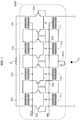
- an input distributed active transformer IN-DAT may include a primary "coil” 10 which may in fact include a single straight (or linear) electrically conductive (e.g. metal) bar or slab having an intermediate (e.g. median) signal input port IN.
- the IN-DAT primary slab 10 may be (magnetically) coupled to a set of secondary slabs 12 1 , ..., 12 N .
- these secondary slabs may be in a number N equal to the number of the differential elementary uPA cells.
- N 4 so that four secondary slabs 12 1 , 12 2 , 12 3 , 12 4 may be provided.
- the inputs of the (differential) uPA cells DA1, DA2, ... may be coupled to the two ends of the respective secondary slab segments 12 1 , 12 2 , ... while the DC bias voltage (VGG in Figure 3 ) to the uPA cell transistor pairs may be applied at an intermediate (e.g. median) point of the secondary slabs, which may provide an AC ground GND for the uPA input signal (see e.g. the capacitors C11 and C12 in Figure 4 ).
- VVGG DC bias voltage
- a corresponding output DAT structure may be coupled to the (differential) outputs of the uPA cells DA1, DA2, ...
- a DC bias voltage for each transistor pair may be applied to an intermediate (median) point of a corresponding OUT-DAT primary slab segment 14 1 , 14 2 , ..., 14 N , which may provide an AC ground GND for the (differential) output signal of the respective uPA cell (see e.g. the capacitors C21 and C22 in Figure 4 .
- each primary slab 14 1 , 14 2 , ..., 14 N , of the output DAT section, OUT-DAT in Figures 3 and 4 may be (magnetically) coupled to the OUT-DAT secondary side which may include a single straight (or linear) electrically conductive (e.g. metal) bar or slab 16.
- such an electrically conductive bar or slab 16 may produce thus a mixed power combination (MCT) of the output signals form the uPA cells DA1, DA2, ...
- MCT mixed power combination
- the overall output signal from the L-DDAT power amplifier may be obtained at an intermediate (e.g. median) point OUT of the secondary slab 16 of the output DAT, namely OUT-DAT.
- a L-DDAT power amplifier arrangement as exemplified in Figures 3 and 4 may facilitate simplifying a RF power amplifier and preamplifier circuit and design methodology by resorting an architecture which may be compact and easy to integrate, while also facilitating targeting different power level through a simple modular approach working up to millimeter-wave frequencies.
- One or more embodiments may maintain the advantage of mitigating transistor breakdown issues, thus facilitating increasing the delivered output power.
- One or more embodiments may thus provide a distributed active transformer including an input transformer set (e.g. IN-DAT) and an output transformer set (e.g. OUT-DAT) and a plurality of active stages (e.g. DA1,..., DAN in Figure 3 or DA1, DA2, DA3, DA4 in Figure 4 ), each active stage being set between a transformer (e.g. T11, ..., T1N; T11, T12, T13, T14) in the input transformer set and a transformer (e.g.
- a transformer e.g. T11, ..., T1N; T11, T12, T13, T14
- both of said input transformer set and said output transformer set may include a slab transformer, with:
- the single primary slab of said input transformer set may include an intermediate signal input port (e.g. IN) thereby providing input signal distribution over said plurality of secondary slabs and said plurality of active stages.
- an intermediate signal input port e.g. IN
- the single secondary slab of said output transformer set may include an intermediate signal output port (e.g. OUT) thereby providing output signal combination from said plurality of primary slabs and said plurality of active stages.
- an intermediate signal output port e.g. OUT
- the active stages in said plurality of active stages may have their inputs coupled to a respective one of said secondary slabs in said plurality of secondary slabs of the input transformer set, optionally with an active stage DC bias voltage (e.g. VGG) applied at an intermediate point of said respective one of said secondary slabs in said plurality of secondary slabs.
- an active stage DC bias voltage e.g. VGG
- the active stages in said plurality of active stages may have their outputs coupled to a respective one of said primary slabs in said plurality of primary slabs of the output transformer set, optionally with an active stage DC bias voltage (e.g. VDD) applied at an intermediate point of said respective one of said primary slabs in said plurality of primary slabs.
- an active stage DC bias voltage e.g. VDD
- said slabs may include linear slabs.
- a segment or portion including electrically conductive material (e.g. metal) and parallel to a straight line extending between the ends thereof may be exemplary of such a linear slab.
- said slabs may include electrically conductive material (e.g. metal material).
- a distributed active transformer as exemplified previously may be implemented as an integrated circuit.
- amplifier apparatus e.g. a power amplifier, e.g. an integrated circuit - IC RF power amplifier for use in a mobile terminal, for instance
- amplifier apparatus may include a distributed active transformer as exemplified previously.
- a method of providing a distributed active transformer may include:
Landscapes
- Engineering & Computer Science (AREA)
- Power Engineering (AREA)
- Microelectronics & Electronic Packaging (AREA)
- Amplifiers (AREA)
- Filters And Equalizers (AREA)
- Housings And Mounting Of Transformers (AREA)
- Coils Or Transformers For Communication (AREA)
Abstract
Description
- The description relates to active transformers.
- One or more embodiments may find use in a variety of applications such as e.g. radio frequency (RF) power amplifiers (PAs).
- Power amplifiers for use in the RF PA market, such as CMOS-based RF power amplifiers for mobile terminals, e.g. in the E-band (81-86 GHz) may be exemplary of such applications.
- Selecting a power amplifier architecture may represent a complex task, involving a judicious compromise of various factors such as e.g. area occupation, efficiency, reliability and maximum output power.
- So-called double distributed active transformers (DDAT's) have been proposed for use e.g. in millimeter-wave power amplifiers.
- Despite the continued activity in that area, the need is still felt for improved solutions which may facilitate, e.g.:
- delivering a high output power with a low-power supply, e.g. by combining power from a plurality of active stages,
- overcoming voltage/current constraints due e.g. to transistor breakdown issues,
- reducing complexity of ultra-high frequency RF PA design, as possibly related to the electromagnetic (EM) domain,
- overcoming the limitations due to the space occupied by spiral inductors and transformers.
- An object of one or more embodiments is to meet such a demand for improvement.
- According to one or more embodiments, that object may be achieved by means of a double distributed active transformer (DDAT) having the features set forth in the claims that follow.
- One or more embodiments may also relate to corresponding apparatus: a power amplifier, e.g. an integrated circuit - IC RF power amplifier for use in a mobile terminal, for instance, may be exemplary of such apparatus.
- One or more embodiments may also relate to a corresponding method.
- The claims are an integral part of the disclosure of one or more embodiments as provided herein.
- In one or more embodiments, a "linear" double distributed active transformer (L-DDAT) may facilitate, e.g.:
- leveraging silicon-based technologies, especially as regards the capability of mitigating transistor breakdown issues, thus increasing the output power delivered,
- simplifying RF power amplifier and preamplifier circuits and the related design activity,
- providing an architecture which is compact and easy to integrate,
- targeting different power levels via a simple modular approach up to millimeter-wave frequencies,
- reducing the power amplifier silicon chip area.
- One or more embodiments may rely on a power combiner topology for reasons such as:
- making it easier to obtain a high output power at millimetre-wave frequencies by combining the outputs from multiple small power amplifier (so-called "micro" power amplifiers or uPA's): each individual uPA cell can be realized with transistors of smaller sizes, providing improved performance, e.g. in terms of higher stable gain and transition frequency; also, such cells can be more easily matched to achieve simultaneously high gain (conjugate matching) and high output power (power matching);
- a power combiner topology may reduce the load impedance at the output of each uPA cell and deliver a relatively high output power through a low voltage supply related to the low breakdown limits of e.g. high speed CMOS and BiCMOS technology.
- One or more embodiments will now be described, by way of example only, with reference to the annexed figures, wherein:
-
Figure 1 is an exemplary circuit diagram of a double distributed active transformer; -
Figure 2 is exemplary of the possible layout of a power divider in driving an active transformer; -
Figure 3 is an exemplary block diagram of one or more embodiments; and -
Figure 4 is a schematic circuit diagram of one or more embodiments. - In the ensuing description, one or more specific details are illustrated, aimed at providing an in-depth understanding of examples of embodiments of the present description. The embodiments may be obtained without one or more of the specific details, or with other methods, components, materials, etc. In other cases, known structures, materials, or operations are not illustrated or described in detail so that certain aspects of embodiments will not be obscured.
- Reference to "an embodiment" or "one embodiment" in the framework of the present description is intended to indicate that a particular configuration, structure, or characteristic described in relation to the embodiment is comprised in at least one embodiment. Hence, phrases such as "in an embodiment" or "in one embodiment" that may be present in one or more points of the present description do not necessarily refer to one and the same embodiment. Moreover, particular conformations, structures, or characteristics may be combined in any adequate way in one or more embodiments.
- The references used herein are provided merely for convenience and hence do not define the extent of protection or the scope of the embodiments.
- Several power combiner concepts exploiting transformers have been proposed in the literature, where transformer secondary outputs have been shown to be connected a load impedance in series, parallel and mixed modes.
- The type of transformer connection may change the impedance seen by the output of each active stage (e.g. MOSFET), while the output powers of the various elementary cells (e.g. uPA's) may be combined and summed together by maintaining the voltage across them within the limits related to the low breakdown voltage of silicon-based technologies such as CMOS and BiCMOS.
- For instance, in the case of series combination, the input impedance seen by the each single uPA cell may be reduced by a factor equal to the number of cells M, while the output power may be increased by a factor proportional to M2. Also, transformer-based power combiner architectures facilitate making load impedance matching efficient, thus improving the overall performance of a power amplifier (PA).
- The article I. Aoki, at el.: "Distributed Active Transformer-A new Power-Combining and Impedance-Transformation Technique", IEEE Trans. on Microwave Theory and Techniques, vol. 50(1), pp. 316-331, 2002 discloses a distributed active transformer (DAT) which allows simultaneously combining power and transforming load impedance to an adequate value for by each single uPA cell.
- Despite the significant advantages of DAT-based power combining structures, feeding the input signal to each single uPA cell input with a minimum phase mismatch and without degrading overall PA stability may be a challenging issue and may require a large area: see e.g. U. R. Pfeiffer, et al.: "A 23-dBm 60-GHz Distributed Active Transformer in a Silicon Process Technology", IEEE Trans. Microw. Theory and Tech., vol. 55(5), pp. 857-865, 2007.
- Document
US 8 049 564 B1 discloses a dual concentric DAT structure (Double Distributed Active Transformer - DDAT) which facilitates achieving improved PA stability, efficiency and minimum area consumption. Also, further details of the possible implementations of a double distributed active transformer layout may be gathered e.g. from A. Pallotta et al.: "Millimeter-Wave 14dBm CMOS Power Amplifier with Input-Output Distributed transformers", CICC2010 (Custom Integrated Circuit Conference), San Jose, CA, 19-22 Sept. 2010, pp. 1 - 4. -
Figure 1 is an exemplary representation of a double distributed active transformer (DDAT) including a "fourfold" DDAT, wherein the primary and secondary windings of an elementary transformer structure are each split (that is, distributed) into four, with four input transformers T11, T12, T13, T14 each driving a respective output transformer T21, T22, T23, T24 via a respective active (amplifier) stage DA1, DA2, DA3, DA4. - As exemplified in
Figure 1 , the primary side of a double distributed active transformer may include the cascaded (e.g. series) arrangement of the primary windings of four transformers T11, T12, T13, T14, optionally with an intermediate tap point between the primary windings of T12 and T13 set to a voltage power supply for proper transistor collector biasing (VCC1). An input (e.g. an input voltage VIN) to the DDAT transformer may thus drive an input current into the primary windings of T11, T12, T13, T14. - In an arrangement as exemplified in
Figure 1 , the secondary windings of the transformers T21, T22, T23, T24 may be cascaded (e.g. series-coupled) to drive a load RL. The load RL may thus be traversed by the current flowing through the secondary windings of the transformers T21, T22, T23, T24. - In the diagram of
Figure 1 , VCC2 and VBB denote respective voltage power supplies coupled with intermediate points of the primary windings of T21, T22, T23, T24 and of the secondary windings of T11, T12, T13, T14. - The resulting power combination may lead to increasing the output power applied to the load RL by a factor of N, where N is the number of transformer elements resulting from splitting/distributing the primary and secondary windings of a basic transformer (e.g. N = 4 in
Figure 1 ). - Likewise, the output voltage on each active device (e.g. transistor) may be divided by a factor of N, thus reducing breakdown stress.
- A difficulty in DAT-based power amplifiers may lie in distributing a RF input signal to all the push-pull couples included in the DAT.
-
Figure 2 is exemplary of the possibility of using a so-called Wilkinson power divider PD, including an input divider stage PD1 having two further divider stages PD21, PD22 cascaded thereto to feed a RF input signal RFin to the active stages PA1, PA2, PA3, PA4 of a distributed active transformer DAT (having a layout different from the layout exemplified inFigure 1 ), including four transformers T1, T2, T3, T4 to produce a RF output signal RFout. - A main drawback of such a Wilkinson power divider (which may also be used in a complementary fashion as a power combiner) - and similar structures - may again lie in the large (e.g. silicon) area required for their layout: for instance a Wilkinson power divider may take the major portion of the chip area and lead to a significant power dissipation.
- One or more embodiments may rely on the recognition that a DAT topology may be implemented using slab transformers, which may facilitate improving efficiency in comparison with conventional transformers based on spiral (coil) inductors. Starting from that recognition, one or more embodiments may exploit a "linear" power splitting and combining architecture as an alternative to the concentric layout disclosed e.g.
US 8 049 564 B1 . - One or more embodiments may thus include a linearly- aligned slab-based DDAT architecture (L-DDAT) as exemplified in
Figures 3 and4 . - For the sake of brevity, certain reference signs already appearing in
Figure 1 have been used inFigures 3 and4 in order to designate the basic elements of an active transformer layout, thus making it unnecessary to repeat here a relative description. - With reference to I. Aoki, at al. (already cited) a transformer-based power combiner including inductor slabs may be easier to optimize for reducing power loss due to metal resistance and impedance mismatching.
- Also, while the concentric or coaxial DDAT of
US 8 049 564 B1 may involve series-connected power splitting and combining slab transformers, a linear DDAT as exemplified inFigures 3 and4 may involve a mixed combination of series and parallel connected slab transformers. This may result in a higher degree of freedom in the design of the output impedance matching network of the individual uPA cells. - In one or more embodiments of a linear DDAT arrangement as exemplified in
Figures 3 and4 , an input distributed active transformer IN-DAT (providing the input power splitting function), may include a primary "coil" 10 which may in fact include a single straight (or linear) electrically conductive (e.g. metal) bar or slab having an intermediate (e.g. median) signal input port IN. - In one or more embodiments, the IN-DAT
primary slab 10 may be (magnetically) coupled to a set ofsecondary slabs 121, ..., 12N. - In one or more embodiments, these secondary slabs may be in a number N equal to the number of the differential elementary uPA cells.
- For instance, in the exemplary implementation of
Figure 4 (as in the DDAT arrangement exemplified inFigure 1 ), N = 4 so that foursecondary slabs - In one or more embodiments, the inputs of the (differential) uPA cells DA1, DA2, ... may be coupled to the two ends of the respective
secondary slab segments Figure 3 ) to the uPA cell transistor pairs may be applied at an intermediate (e.g. median) point of the secondary slabs, which may provide an AC ground GND for the uPA input signal (see e.g. the capacitors C11 and C12 inFigure 4 ). - As in the case of the DDAT architecture concept of
Figure 1 orUS 8 049 564 B1 , in one or more embodiments as exemplified inFigures 3 and4 , a corresponding output DAT structure, indicated OUT-DAT, may be coupled to the (differential) outputs of the uPA cells DA1, DA2, .... - For instance, in one or more embodiments a DC bias voltage for each transistor pair (VDD in
Figure 3 ) may be applied to an intermediate (median) point of a corresponding OUT-DATprimary slab segment Figure 4 . - Again, each
primary slab Figures 3 and4 , may be (magnetically) coupled to the OUT-DAT secondary side which may include a single straight (or linear) electrically conductive (e.g. metal) bar orslab 16. - In one or more embodiments, such an electrically conductive bar or
slab 16 may produce thus a mixed power combination (MCT) of the output signals form the uPA cells DA1, DA2, .... - In one or more embodiments, the overall output signal from the L-DDAT power amplifier may be obtained at an intermediate (e.g. median) point OUT of the
secondary slab 16 of the output DAT, namely OUT-DAT. - In one or more embodiments, a L-DDAT power amplifier arrangement as exemplified in
Figures 3 and4 may facilitate simplifying a RF power amplifier and preamplifier circuit and design methodology by resorting an architecture which may be compact and easy to integrate, while also facilitating targeting different power level through a simple modular approach working up to millimeter-wave frequencies. - One or more embodiments may maintain the advantage of mitigating transistor breakdown issues, thus facilitating increasing the delivered output power.
- One or more embodiments may offer one or more of the following advantages:
- a mixed power-combining transformer (MCT) may be provided as a combination of series and parallel transformers (SCT + PCT) to facilitate increasing the output signal power by properly adjusting the load resistance;
- increasing output power may be facilitated while staying within the low breakdown voltage limits of silicon- based transistor technologies such as e.g. CMOS and BiCMOS;
- a modular design approach may facilitate increasing the number of power stages;
- a simplified and compact layout may be obtained, reducing area consumption;
- a double DAT configuration may facilitate efficient input signal power splitting;
- a localized electro-magnetic (EM) field in slab transformers may reduce cross-talk and passive Q-factor degradation: slab inductors may in facts outperform single loop inductor in terms of Q-factor;
- cross-connection may be reduced through I/O power distribution (1-way signal path);
- a linear DAT layout is well suited for differential I/O connection;
- using a balanced-unbalanced transformer (balun) may no longer be necessary for single-ended input/output connection;
- transformer-based power dividers may dispense with capacitors for AC coupling;
- low area occupation;
- output powers in the range of e.g. P1dB ≥ 22dBm@84GHz may be achieved.
- One or more embodiments may thus provide a distributed active transformer including an input transformer set (e.g. IN-DAT) and an output transformer set (e.g. OUT-DAT) and a plurality of active stages (e.g. DA1,..., DAN in
Figure 3 or DA1, DA2, DA3, DA4 inFigure 4 ), each active stage being set between a transformer (e.g. T11, ..., T1N; T11, T12, T13, T14) in the input transformer set and a transformer (e.g. T21, ..., T2N; T21, T22, T23, T24) in the output transformer set, wherein at least one of said input transformer set and said output transformer set may include a slab transformer with a single primary (e.g. 10) resp. secondary (e.g. 16) slab coupled with a plurality of secondary (e.g. 121, ..., 12N; 121, 122, 123, 124) resp. primary (e.g. 141, ..., 14N; 141, 142, 143, 144) slabs. - In one or more embodiments, both of said input transformer set and said output transformer set may include a slab transformer, with:
- said input transformer set including a single primary slab (e.g. 10) coupled with a plurality of secondary slabs (e.g. 121, ..., 12N; 121, 122, 123, 124), and
- said output transformer set including a plurality of primary slabs (e.g. 141, ..., 14N; 141, 142, 143, 144) coupled with a single secondary slab (e.g. 16).
- In one or more embodiments, the single primary slab of said input transformer set may include an intermediate signal input port (e.g. IN) thereby providing input signal distribution over said plurality of secondary slabs and said plurality of active stages.
- In one or more embodiments, the single secondary slab of said output transformer set may include an intermediate signal output port (e.g. OUT) thereby providing output signal combination from said plurality of primary slabs and said plurality of active stages.
- In one or more embodiments, the active stages in said plurality of active stages may have their inputs coupled to a respective one of said secondary slabs in said plurality of secondary slabs of the input transformer set, optionally with an active stage DC bias voltage (e.g. VGG) applied at an intermediate point of said respective one of said secondary slabs in said plurality of secondary slabs.
- In one or more embodiments, the active stages in said plurality of active stages may have their outputs coupled to a respective one of said primary slabs in said plurality of primary slabs of the output transformer set, optionally with an active stage DC bias voltage (e.g. VDD) applied at an intermediate point of said respective one of said primary slabs in said plurality of primary slabs.
- In one or more embodiments, said slabs may include linear slabs. A segment or portion including electrically conductive material (e.g. metal) and parallel to a straight line extending between the ends thereof may be exemplary of such a linear slab.
- In one or more embodiments, said slabs may include electrically conductive material (e.g. metal material).
- In one or more embodiments, a distributed active transformer as exemplified previously may be implemented as an integrated circuit.
- In one or more embodiments, amplifier apparatus (e.g. a power amplifier, e.g. an integrated circuit - IC RF power amplifier for use in a mobile terminal, for instance) may include a distributed active transformer as exemplified previously.
- In one or more embodiments, a method of providing a distributed active transformer may include:
- providing an input transformer set and an output transformer set and a plurality of active stages by setting each active stage between a transformer in the input transformer set and a transformer in the output transformer set,
- providing at least one, and optionally both, of said input transformer set and said output transformer set including a slab transformer with a single primary resp. secondary slab coupled with a plurality of secondary resp. primary slabs.
- Without prejudice to the underlying principles, the details and embodiments may vary, even significantly, with respect to what has been described by way of example only without departing from the extent of protection.
- The extent of protection is defined by the annexed claims.
Claims (11)
- A distributed active transformer including an input transformer set (IN-DAT) and an output transformer set (OUT-DAT) and a plurality of active stages (DA1, DAN; DA1, DA2, DA3, DA4) with each active stage being set between a transformer (T11, ..., T1N; T11, T12, T13, T14) in the input transformer set (IN-DAT) and a transformer (T21, ..., T2N; T21, T22, T23, T24) in the output transformer set (OUT-DAT), wherein at least one of said input transformer set (IN-DAT) and said output transformer set (OUT-DAT) includes a slab transformer with a single primary (10) resp. secondary (16) slab coupled with a plurality of secondary (121, ..., 12N; 121, 122, 123, 124) resp. primary (141, ..., 14N; 141, 142, 143, 144) slabs.
- The distributed active transformer of claim 1, wherein both of said input transformer set (IN-DAT) and said output transformer set (OUT-DAT) include a slab transformer, with:- said input transformer set (IN-DAT) including a single primary slab (10) coupled with a plurality of secondary slabs (121, ..., 12N; 121, 122, 123, 124), and- said output transformer set (OUT-DAT) including a plurality of primary slabs (141, ..., 14N; 141, 142, 143, 144) coupled with a single secondary slab (16).
- The distributed active transformer of claim 1 or claim 2, wherein the single primary slab (10) of said input transformer set (IN-DAT) includes an intermediate signal input port (IN) thereby providing input signal distribution over said plurality of secondary slabs (121, ..., 12N; 121, 122, 123, 124) and said plurality of active stages (DA1, DAN; DA1, DA2, DA3, DA4).
- The distributed active transformer of any of the previous claims, wherein the single secondary slab (16) of said output transformer set (OUT-DAT) includes an intermediate signal output port (OUT) thereby providing output signal combination from said plurality of primary slabs (141, ..., 14N; 141, 142, 143, 144) and said plurality of active stages (DA1, DAN; DA1, DA2, DA3, DA4).
- The distributed active transformer of any of the previous claims, wherein the active stages in said pluralityof active stages (DA1, DAN; DA1, DA2, DA3, DA4) have their inputs coupled to a respective one of said secondary slabs in said plurality of secondary slabs (121, ..., 12N; 121, 122, 123, 124) of the input transformer set (IN-DAT), preferably with an active stage DC bias voltage (VGG) applied at an intermediate point of said respective one of said secondary slabs in said plurality of secondary slabs (121, ..., 12N; 121, 122, 123, 124).
- The distributed active transformer of any of the previous claims, wherein the active stages in said plurality of active stages (DA1, DAN; DA1, DA2, DA3, DA4) have their outputs coupled to a respective one of said primary slabs in said plurality of primary slabs (141, ..., 142N; 141, 142, 143, 144) of the output transformer set (OUT-DAT), preferably with an active stage DC bias voltage (VDD) applied at an intermediate point of said respective one of said primary slabs in said plurality of primary slabs (141, ..., 14N; 141, 142, 143, 144).
- The distributed active transformer of any of the previous claims, wherein said slabs (10; 16; 121, ..., 12N; 121, 122, 123, 124; 141, ..., 14N; 141, 142, 143, 144) include linear slabs.
- The distributed active transformer of any of the previous claims, wherein said slabs (10; 16; 121, ..., 12N; 121, 122, 123, 124; 141, ..., 14N; 141, 142, 143, 144) include electrically conductive material.
- The distributed active transformer of any of the previous claims, wherein the transformer is implemented as an integrated circuit.
- Amplifier apparatus including a distributed active transformer according to any of claims 1 to 9.
- A method of providing a distributed active transformer including:- providing an input transformer set (IN-DAT) and an output transformer set (OUT-DAT) and a plurality of active stages (DA1, DAN; DA1, DA2, DA3, DA4) by setting each active stage between a transformer (T11, ..., T1N; T11, T12, T13, T14) in the input transformer set (IN-DAT) and a transformer (T21, ..., T2N; T21, T22, T23, T24) in the output transformer set (OUT-DAT),- providing at least one, and preferably both, of said input transformer set (IN-DAT) and said output transformer set (OUT-DAT) including a slab transformer with a single primary (10) resp. secondary (16) slab coupled with a plurality of secondary (121, ..., 12N; 121, 122, 123, 124) resp. primary (141, ..., 14N; 141, 142, 143, 144) slabs.
Applications Claiming Priority (1)
| Application Number | Priority Date | Filing Date | Title |
|---|---|---|---|
| ITUA2016A003549A ITUA20163549A1 (en) | 2016-05-18 | 2016-05-18 | ACTIVE TRANSFORMER, EQUIPMENT AND CORRESPONDENT PROCEDURE |
Publications (2)
| Publication Number | Publication Date |
|---|---|
| EP3247041A1 true EP3247041A1 (en) | 2017-11-22 |
| EP3247041B1 EP3247041B1 (en) | 2020-09-02 |
Family
ID=56853763
Family Applications (1)
| Application Number | Title | Priority Date | Filing Date |
|---|---|---|---|
| EP17170096.6A Active EP3247041B1 (en) | 2016-05-18 | 2017-05-09 | An active transformer, corresponding apparatus and method |
Country Status (3)
| Country | Link |
|---|---|
| US (1) | US10236845B2 (en) |
| EP (1) | EP3247041B1 (en) |
| IT (1) | ITUA20163549A1 (en) |
Cited By (2)
| Publication number | Priority date | Publication date | Assignee | Title |
|---|---|---|---|---|
| EP3579410A1 (en) * | 2018-06-07 | 2019-12-11 | Ion Beam Applications | High power solid state rf amplifier |
| US10574287B1 (en) | 2018-09-28 | 2020-02-25 | Qualcomm Incorporated | Wireless transceiver with reconfigurable transformers |
Families Citing this family (1)
| Publication number | Priority date | Publication date | Assignee | Title |
|---|---|---|---|---|
| NL2021654B1 (en) * | 2018-09-18 | 2020-05-07 | Prodrive Tech Bv | Balun transformer |
Citations (3)
| Publication number | Priority date | Publication date | Assignee | Title |
|---|---|---|---|---|
| US8049564B2 (en) | 2008-12-30 | 2011-11-01 | Stmicroelectronics S.R.L. | Distributed active transformer amplifier with differential power combiner |
| US20130099864A1 (en) * | 2010-06-21 | 2013-04-25 | Panasonic Corporation | Power amplifier |
| US20150214994A1 (en) * | 2014-01-30 | 2015-07-30 | National Taiwan University | Three-dimensional power amplifier architecture |
Family Cites Families (6)
| Publication number | Priority date | Publication date | Assignee | Title |
|---|---|---|---|---|
| US5789996A (en) * | 1997-04-02 | 1998-08-04 | Harris Corporation | N-way RF power combiner/divider |
| US6856199B2 (en) * | 2000-10-10 | 2005-02-15 | California Institute Of Technology | Reconfigurable distributed active transformers |
| US7095283B2 (en) * | 2003-10-28 | 2006-08-22 | Axiom Microdevices, Inc. | Supply circuit for power amplifier drivers |
| US8125276B2 (en) * | 2010-03-12 | 2012-02-28 | Samsung Electro-Mechanics | Sharing of inductor interstage matching in parallel amplification system for wireless communication systems |
| US8319556B2 (en) * | 2010-11-09 | 2012-11-27 | Raytheon Company | Transformer coupled distributed amplifier |
| US8634782B2 (en) * | 2011-10-14 | 2014-01-21 | Qualcomm Incorporated | Multi-antenna wireless device with power combining power amplifiers |
-
2016
- 2016-05-18 IT ITUA2016A003549A patent/ITUA20163549A1/en unknown
- 2016-11-29 US US15/363,633 patent/US10236845B2/en active Active
-
2017
- 2017-05-09 EP EP17170096.6A patent/EP3247041B1/en active Active
Patent Citations (3)
| Publication number | Priority date | Publication date | Assignee | Title |
|---|---|---|---|---|
| US8049564B2 (en) | 2008-12-30 | 2011-11-01 | Stmicroelectronics S.R.L. | Distributed active transformer amplifier with differential power combiner |
| US20130099864A1 (en) * | 2010-06-21 | 2013-04-25 | Panasonic Corporation | Power amplifier |
| US20150214994A1 (en) * | 2014-01-30 | 2015-07-30 | National Taiwan University | Three-dimensional power amplifier architecture |
Non-Patent Citations (3)
| Title |
|---|
| A. PALLOTTA ET AL.: "Millimeter-Wave 14dBm CMOS Power Amplifier with Input-Output Distributed transformers", CICC2010 (CUSTOM INTEGRATED CIRCUIT CONFERENCE, 19 September 2010 (2010-09-19), pages 1 - 4, XP031786641 |
| I. AOKI: "Distributed Active Transformer-A new Power-Combining and Impedance- Transformation Technique", IEEE TRANS. ON MICROWAVE THEORY AND TECHNIQUES, vol. 50, no. 1, 2002, pages 316 - 331, XP001085553, DOI: doi:10.1109/22.981284 |
| U. R. PFEIFFER ET AL.: "A 23-dBm 60-GHz Distributed Active Transformer in a Silicon Process Technology", IEEE TRANS. MICROW. THEORY AND TECH., vol. 55, no. 5, 2007, pages 857 - 865, XP011180989, DOI: doi:10.1109/TMTT.2007.895654 |
Cited By (2)
| Publication number | Priority date | Publication date | Assignee | Title |
|---|---|---|---|---|
| EP3579410A1 (en) * | 2018-06-07 | 2019-12-11 | Ion Beam Applications | High power solid state rf amplifier |
| US10574287B1 (en) | 2018-09-28 | 2020-02-25 | Qualcomm Incorporated | Wireless transceiver with reconfigurable transformers |
Also Published As
| Publication number | Publication date |
|---|---|
| US10236845B2 (en) | 2019-03-19 |
| US20170338783A1 (en) | 2017-11-23 |
| EP3247041B1 (en) | 2020-09-02 |
| ITUA20163549A1 (en) | 2017-11-18 |
Similar Documents
| Publication | Publication Date | Title |
|---|---|---|
| US7068104B2 (en) | Power amplifier utilizing high breakdown voltage circuit topology | |
| US6816012B2 (en) | Distributed circular geometry power amplifier architecture | |
| CN101764581B (en) | Integrated power amplifier for use in wireless communication devices | |
| CN108462477B (en) | Power amplifying circuit | |
| US8319556B2 (en) | Transformer coupled distributed amplifier | |
| Park et al. | A 1.9-GHz CMOS power amplifier using three-port asymmetric transmission line transformer for a polar transmitter | |
| US20120139640A1 (en) | Bond wire transformer | |
| US20150372645A1 (en) | Class-e outphasing power amplifier with efficiency and output power enhancement circuits and method | |
| EP3939161A1 (en) | Power amplifier arrangement | |
| US7486141B2 (en) | Wide bandwidth, high power amplifier | |
| CN110690859A (en) | Power amplifying circuit | |
| Levy et al. | A 14-GHz, 22-dBm series Doherty power amplifier in 45-nm CMOS SOI | |
| EP3247041B1 (en) | An active transformer, corresponding apparatus and method | |
| KR20230129028A (en) | High-efficiency dual-drive power amplifier for high-reliability applications | |
| US20060006945A1 (en) | Parallel amplifier configuration with power combining and impedance transformation | |
| US12261573B2 (en) | Amplifier with stacked transconducting cells in current mode combining | |
| Kaymaksüt et al. | A 2.4 GHz fully integrated Doherty power amplifier using series combining transformer | |
| Ren et al. | A novel stacked class-E-like power amplifier with dual drain output power technique in 0.18 um RFSOI CMOS technology | |
| EP4120564A1 (en) | Amplifier with stacked transconducting cells in parallel and/or cascade current mode combining | |
| Murad et al. | High efficiency CMOS class-E power amplifiers in gigahertz frequencies: A review | |
| JP2019220777A (en) | Wireless transmission device and wireless communication device | |
| EP3829059B1 (en) | Power combiner circuit and method | |
| Das et al. | Design of an MMIC Medium Power Amplifier at 47 GHz | |
| Pei et al. | A 60GHz fully integrated power amplifier using a distributed ring transformer in CMOS 65nm |
Legal Events
| Date | Code | Title | Description |
|---|---|---|---|
| PUAI | Public reference made under article 153(3) epc to a published international application that has entered the european phase |
Free format text: ORIGINAL CODE: 0009012 |
|
| STAA | Information on the status of an ep patent application or granted ep patent |
Free format text: STATUS: THE APPLICATION HAS BEEN PUBLISHED |
|
| AK | Designated contracting states |
Kind code of ref document: A1 Designated state(s): AL AT BE BG CH CY CZ DE DK EE ES FI FR GB GR HR HU IE IS IT LI LT LU LV MC MK MT NL NO PL PT RO RS SE SI SK SM TR |
|
| AX | Request for extension of the european patent |
Extension state: BA ME |
|
| STAA | Information on the status of an ep patent application or granted ep patent |
Free format text: STATUS: REQUEST FOR EXAMINATION WAS MADE |
|
| 17P | Request for examination filed |
Effective date: 20180416 |
|
| RBV | Designated contracting states (corrected) |
Designated state(s): AL AT BE BG CH CY CZ DE DK EE ES FI FR GB GR HR HU IE IS IT LI LT LU LV MC MK MT NL NO PL PT RO RS SE SI SK SM TR |
|
| GRAP | Despatch of communication of intention to grant a patent |
Free format text: ORIGINAL CODE: EPIDOSNIGR1 |
|
| STAA | Information on the status of an ep patent application or granted ep patent |
Free format text: STATUS: GRANT OF PATENT IS INTENDED |
|
| INTG | Intention to grant announced |
Effective date: 20200414 |
|
| GRAS | Grant fee paid |
Free format text: ORIGINAL CODE: EPIDOSNIGR3 |
|
| GRAA | (expected) grant |
Free format text: ORIGINAL CODE: 0009210 |
|
| STAA | Information on the status of an ep patent application or granted ep patent |
Free format text: STATUS: THE PATENT HAS BEEN GRANTED |
|
| AK | Designated contracting states |
Kind code of ref document: B1 Designated state(s): AL AT BE BG CH CY CZ DE DK EE ES FI FR GB GR HR HU IE IS IT LI LT LU LV MC MK MT NL NO PL PT RO RS SE SI SK SM TR |
|
| REG | Reference to a national code |
Ref country code: GB Ref legal event code: FG4D |
|
| REG | Reference to a national code |
Ref country code: AT Ref legal event code: REF Ref document number: 1309981 Country of ref document: AT Kind code of ref document: T Effective date: 20200915 Ref country code: CH Ref legal event code: EP |
|
| REG | Reference to a national code |
Ref country code: DE Ref legal event code: R096 Ref document number: 602017022623 Country of ref document: DE |
|
| REG | Reference to a national code |
Ref country code: IE Ref legal event code: FG4D |
|
| REG | Reference to a national code |
Ref country code: LT Ref legal event code: MG4D |
|
| PG25 | Lapsed in a contracting state [announced via postgrant information from national office to epo] |
Ref country code: FI Free format text: LAPSE BECAUSE OF FAILURE TO SUBMIT A TRANSLATION OF THE DESCRIPTION OR TO PAY THE FEE WITHIN THE PRESCRIBED TIME-LIMIT Effective date: 20200902 Ref country code: LT Free format text: LAPSE BECAUSE OF FAILURE TO SUBMIT A TRANSLATION OF THE DESCRIPTION OR TO PAY THE FEE WITHIN THE PRESCRIBED TIME-LIMIT Effective date: 20200902 Ref country code: BG Free format text: LAPSE BECAUSE OF FAILURE TO SUBMIT A TRANSLATION OF THE DESCRIPTION OR TO PAY THE FEE WITHIN THE PRESCRIBED TIME-LIMIT Effective date: 20201202 Ref country code: NO Free format text: LAPSE BECAUSE OF FAILURE TO SUBMIT A TRANSLATION OF THE DESCRIPTION OR TO PAY THE FEE WITHIN THE PRESCRIBED TIME-LIMIT Effective date: 20201202 Ref country code: GR Free format text: LAPSE BECAUSE OF FAILURE TO SUBMIT A TRANSLATION OF THE DESCRIPTION OR TO PAY THE FEE WITHIN THE PRESCRIBED TIME-LIMIT Effective date: 20201203 Ref country code: HR Free format text: LAPSE BECAUSE OF FAILURE TO SUBMIT A TRANSLATION OF THE DESCRIPTION OR TO PAY THE FEE WITHIN THE PRESCRIBED TIME-LIMIT Effective date: 20200902 Ref country code: SE Free format text: LAPSE BECAUSE OF FAILURE TO SUBMIT A TRANSLATION OF THE DESCRIPTION OR TO PAY THE FEE WITHIN THE PRESCRIBED TIME-LIMIT Effective date: 20200902 |
|
| REG | Reference to a national code |
Ref country code: NL Ref legal event code: MP Effective date: 20200902 |
|
| REG | Reference to a national code |
Ref country code: AT Ref legal event code: MK05 Ref document number: 1309981 Country of ref document: AT Kind code of ref document: T Effective date: 20200902 |
|
| PG25 | Lapsed in a contracting state [announced via postgrant information from national office to epo] |
Ref country code: RS Free format text: LAPSE BECAUSE OF FAILURE TO SUBMIT A TRANSLATION OF THE DESCRIPTION OR TO PAY THE FEE WITHIN THE PRESCRIBED TIME-LIMIT Effective date: 20200902 Ref country code: PL Free format text: LAPSE BECAUSE OF FAILURE TO SUBMIT A TRANSLATION OF THE DESCRIPTION OR TO PAY THE FEE WITHIN THE PRESCRIBED TIME-LIMIT Effective date: 20200902 Ref country code: LV Free format text: LAPSE BECAUSE OF FAILURE TO SUBMIT A TRANSLATION OF THE DESCRIPTION OR TO PAY THE FEE WITHIN THE PRESCRIBED TIME-LIMIT Effective date: 20200902 |
|
| PG25 | Lapsed in a contracting state [announced via postgrant information from national office to epo] |
Ref country code: SM Free format text: LAPSE BECAUSE OF FAILURE TO SUBMIT A TRANSLATION OF THE DESCRIPTION OR TO PAY THE FEE WITHIN THE PRESCRIBED TIME-LIMIT Effective date: 20200902 Ref country code: EE Free format text: LAPSE BECAUSE OF FAILURE TO SUBMIT A TRANSLATION OF THE DESCRIPTION OR TO PAY THE FEE WITHIN THE PRESCRIBED TIME-LIMIT Effective date: 20200902 Ref country code: CZ Free format text: LAPSE BECAUSE OF FAILURE TO SUBMIT A TRANSLATION OF THE DESCRIPTION OR TO PAY THE FEE WITHIN THE PRESCRIBED TIME-LIMIT Effective date: 20200902 Ref country code: PT Free format text: LAPSE BECAUSE OF FAILURE TO SUBMIT A TRANSLATION OF THE DESCRIPTION OR TO PAY THE FEE WITHIN THE PRESCRIBED TIME-LIMIT Effective date: 20210104 Ref country code: RO Free format text: LAPSE BECAUSE OF FAILURE TO SUBMIT A TRANSLATION OF THE DESCRIPTION OR TO PAY THE FEE WITHIN THE PRESCRIBED TIME-LIMIT Effective date: 20200902 |
|
| PG25 | Lapsed in a contracting state [announced via postgrant information from national office to epo] |
Ref country code: AL Free format text: LAPSE BECAUSE OF FAILURE TO SUBMIT A TRANSLATION OF THE DESCRIPTION OR TO PAY THE FEE WITHIN THE PRESCRIBED TIME-LIMIT Effective date: 20200902 Ref country code: AT Free format text: LAPSE BECAUSE OF FAILURE TO SUBMIT A TRANSLATION OF THE DESCRIPTION OR TO PAY THE FEE WITHIN THE PRESCRIBED TIME-LIMIT Effective date: 20200902 Ref country code: ES Free format text: LAPSE BECAUSE OF FAILURE TO SUBMIT A TRANSLATION OF THE DESCRIPTION OR TO PAY THE FEE WITHIN THE PRESCRIBED TIME-LIMIT Effective date: 20200902 Ref country code: IS Free format text: LAPSE BECAUSE OF FAILURE TO SUBMIT A TRANSLATION OF THE DESCRIPTION OR TO PAY THE FEE WITHIN THE PRESCRIBED TIME-LIMIT Effective date: 20210102 |
|
| REG | Reference to a national code |
Ref country code: DE Ref legal event code: R097 Ref document number: 602017022623 Country of ref document: DE |
|
| PG25 | Lapsed in a contracting state [announced via postgrant information from national office to epo] |
Ref country code: SK Free format text: LAPSE BECAUSE OF FAILURE TO SUBMIT A TRANSLATION OF THE DESCRIPTION OR TO PAY THE FEE WITHIN THE PRESCRIBED TIME-LIMIT Effective date: 20200902 |
|
| PLBE | No opposition filed within time limit |
Free format text: ORIGINAL CODE: 0009261 |
|
| STAA | Information on the status of an ep patent application or granted ep patent |
Free format text: STATUS: NO OPPOSITION FILED WITHIN TIME LIMIT |
|
| 26N | No opposition filed |
Effective date: 20210603 |
|
| PG25 | Lapsed in a contracting state [announced via postgrant information from national office to epo] |
Ref country code: DK Free format text: LAPSE BECAUSE OF FAILURE TO SUBMIT A TRANSLATION OF THE DESCRIPTION OR TO PAY THE FEE WITHIN THE PRESCRIBED TIME-LIMIT Effective date: 20200902 Ref country code: SI Free format text: LAPSE BECAUSE OF FAILURE TO SUBMIT A TRANSLATION OF THE DESCRIPTION OR TO PAY THE FEE WITHIN THE PRESCRIBED TIME-LIMIT Effective date: 20200902 |
|
| PG25 | Lapsed in a contracting state [announced via postgrant information from national office to epo] |
Ref country code: IT Free format text: LAPSE BECAUSE OF FAILURE TO SUBMIT A TRANSLATION OF THE DESCRIPTION OR TO PAY THE FEE WITHIN THE PRESCRIBED TIME-LIMIT Effective date: 20200902 |
|
| REG | Reference to a national code |
Ref country code: CH Ref legal event code: PL |
|
| GBPC | Gb: european patent ceased through non-payment of renewal fee |
Effective date: 20210509 |
|
| PG25 | Lapsed in a contracting state [announced via postgrant information from national office to epo] |
Ref country code: CH Free format text: LAPSE BECAUSE OF NON-PAYMENT OF DUE FEES Effective date: 20210531 Ref country code: MC Free format text: LAPSE BECAUSE OF FAILURE TO SUBMIT A TRANSLATION OF THE DESCRIPTION OR TO PAY THE FEE WITHIN THE PRESCRIBED TIME-LIMIT Effective date: 20200902 Ref country code: LU Free format text: LAPSE BECAUSE OF NON-PAYMENT OF DUE FEES Effective date: 20210509 Ref country code: LI Free format text: LAPSE BECAUSE OF NON-PAYMENT OF DUE FEES Effective date: 20210531 |
|
| REG | Reference to a national code |
Ref country code: BE Ref legal event code: MM Effective date: 20210531 |
|
| PG25 | Lapsed in a contracting state [announced via postgrant information from national office to epo] |
Ref country code: IE Free format text: LAPSE BECAUSE OF NON-PAYMENT OF DUE FEES Effective date: 20210509 Ref country code: GB Free format text: LAPSE BECAUSE OF NON-PAYMENT OF DUE FEES Effective date: 20210509 |
|
| PG25 | Lapsed in a contracting state [announced via postgrant information from national office to epo] |
Ref country code: FR Free format text: LAPSE BECAUSE OF NON-PAYMENT OF DUE FEES Effective date: 20210531 |
|
| PG25 | Lapsed in a contracting state [announced via postgrant information from national office to epo] |
Ref country code: BE Free format text: LAPSE BECAUSE OF NON-PAYMENT OF DUE FEES Effective date: 20210531 |
|
| PG25 | Lapsed in a contracting state [announced via postgrant information from national office to epo] |
Ref country code: HU Free format text: LAPSE BECAUSE OF FAILURE TO SUBMIT A TRANSLATION OF THE DESCRIPTION OR TO PAY THE FEE WITHIN THE PRESCRIBED TIME-LIMIT; INVALID AB INITIO Effective date: 20170509 |
|
| PG25 | Lapsed in a contracting state [announced via postgrant information from national office to epo] |
Ref country code: NL Free format text: LAPSE BECAUSE OF NON-PAYMENT OF DUE FEES Effective date: 20200923 Ref country code: CY Free format text: LAPSE BECAUSE OF FAILURE TO SUBMIT A TRANSLATION OF THE DESCRIPTION OR TO PAY THE FEE WITHIN THE PRESCRIBED TIME-LIMIT Effective date: 20200902 |
|
| PG25 | Lapsed in a contracting state [announced via postgrant information from national office to epo] |
Ref country code: MK Free format text: LAPSE BECAUSE OF FAILURE TO SUBMIT A TRANSLATION OF THE DESCRIPTION OR TO PAY THE FEE WITHIN THE PRESCRIBED TIME-LIMIT Effective date: 20200902 |
|
| PG25 | Lapsed in a contracting state [announced via postgrant information from national office to epo] |
Ref country code: TR Free format text: LAPSE BECAUSE OF FAILURE TO SUBMIT A TRANSLATION OF THE DESCRIPTION OR TO PAY THE FEE WITHIN THE PRESCRIBED TIME-LIMIT Effective date: 20200902 |
|
| PG25 | Lapsed in a contracting state [announced via postgrant information from national office to epo] |
Ref country code: MT Free format text: LAPSE BECAUSE OF FAILURE TO SUBMIT A TRANSLATION OF THE DESCRIPTION OR TO PAY THE FEE WITHIN THE PRESCRIBED TIME-LIMIT Effective date: 20200902 |
|
| PGFP | Annual fee paid to national office [announced via postgrant information from national office to epo] |
Ref country code: DE Payment date: 20250423 Year of fee payment: 9 |