EP3246951A1 - Semiconductor structure - Google Patents
Semiconductor structure Download PDFInfo
- Publication number
- EP3246951A1 EP3246951A1 EP17169363.3A EP17169363A EP3246951A1 EP 3246951 A1 EP3246951 A1 EP 3246951A1 EP 17169363 A EP17169363 A EP 17169363A EP 3246951 A1 EP3246951 A1 EP 3246951A1
- Authority
- EP
- European Patent Office
- Prior art keywords
- fins
- polys
- semiconductor structure
- circuit
- guard ring
- Prior art date
- Legal status (The legal status is an assumption and is not a legal conclusion. Google has not performed a legal analysis and makes no representation as to the accuracy of the status listed.)
- Granted
Links
Images



Classifications
-
- H—ELECTRICITY
- H10—SEMICONDUCTOR DEVICES; ELECTRIC SOLID-STATE DEVICES NOT OTHERWISE PROVIDED FOR
- H10D—INORGANIC ELECTRIC SEMICONDUCTOR DEVICES
- H10D84/00—Integrated devices formed in or on semiconductor substrates that comprise only semiconducting layers, e.g. on Si wafers or on GaAs-on-Si wafers
- H10D84/80—Integrated devices formed in or on semiconductor substrates that comprise only semiconducting layers, e.g. on Si wafers or on GaAs-on-Si wafers characterised by the integration of at least one component covered by groups H10D12/00 or H10D30/00, e.g. integration of IGFETs
- H10D84/82—Integrated devices formed in or on semiconductor substrates that comprise only semiconducting layers, e.g. on Si wafers or on GaAs-on-Si wafers characterised by the integration of at least one component covered by groups H10D12/00 or H10D30/00, e.g. integration of IGFETs of only field-effect components
- H10D84/83—Integrated devices formed in or on semiconductor substrates that comprise only semiconducting layers, e.g. on Si wafers or on GaAs-on-Si wafers characterised by the integration of at least one component covered by groups H10D12/00 or H10D30/00, e.g. integration of IGFETs of only field-effect components of only insulated-gate FETs [IGFET]
- H10D84/85—Complementary IGFETs, e.g. CMOS
- H10D84/853—Complementary IGFETs, e.g. CMOS comprising FinFETs
-
- H—ELECTRICITY
- H10—SEMICONDUCTOR DEVICES; ELECTRIC SOLID-STATE DEVICES NOT OTHERWISE PROVIDED FOR
- H10W—GENERIC PACKAGES, INTERCONNECTIONS, CONNECTORS OR OTHER CONSTRUCTIONAL DETAILS OF DEVICES COVERED BY CLASS H10
- H10W42/00—Arrangements for protection of devices
-
- H—ELECTRICITY
- H10—SEMICONDUCTOR DEVICES; ELECTRIC SOLID-STATE DEVICES NOT OTHERWISE PROVIDED FOR
- H10D—INORGANIC ELECTRIC SEMICONDUCTOR DEVICES
- H10D1/00—Resistors, capacitors or inductors
-
- H—ELECTRICITY
- H10—SEMICONDUCTOR DEVICES; ELECTRIC SOLID-STATE DEVICES NOT OTHERWISE PROVIDED FOR
- H10D—INORGANIC ELECTRIC SEMICONDUCTOR DEVICES
- H10D30/00—Field-effect transistors [FET]
- H10D30/01—Manufacture or treatment
- H10D30/021—Manufacture or treatment of FETs having insulated gates [IGFET]
- H10D30/024—Manufacture or treatment of FETs having insulated gates [IGFET] of fin field-effect transistors [FinFET]
- H10D30/0243—Manufacture or treatment of FETs having insulated gates [IGFET] of fin field-effect transistors [FinFET] using dummy structures having essentially the same shapes as the semiconductor bodies, e.g. to provide stability
-
- H—ELECTRICITY
- H10—SEMICONDUCTOR DEVICES; ELECTRIC SOLID-STATE DEVICES NOT OTHERWISE PROVIDED FOR
- H10D—INORGANIC ELECTRIC SEMICONDUCTOR DEVICES
- H10D30/00—Field-effect transistors [FET]
- H10D30/60—Insulated-gate field-effect transistors [IGFET]
- H10D30/62—Fin field-effect transistors [FinFET]
-
- H—ELECTRICITY
- H10—SEMICONDUCTOR DEVICES; ELECTRIC SOLID-STATE DEVICES NOT OTHERWISE PROVIDED FOR
- H10D—INORGANIC ELECTRIC SEMICONDUCTOR DEVICES
- H10D62/00—Semiconductor bodies, or regions thereof, of devices having potential barriers
- H10D62/10—Shapes, relative sizes or dispositions of the regions of the semiconductor bodies; Shapes of the semiconductor bodies
- H10D62/102—Constructional design considerations for preventing surface leakage or controlling electric field concentration
- H10D62/103—Constructional design considerations for preventing surface leakage or controlling electric field concentration for increasing or controlling the breakdown voltage of reverse-biased devices
- H10D62/105—Constructional design considerations for preventing surface leakage or controlling electric field concentration for increasing or controlling the breakdown voltage of reverse-biased devices by having particular doping profiles, shapes or arrangements of PN junctions; by having supplementary regions, e.g. junction termination extension [JTE]
- H10D62/106—Constructional design considerations for preventing surface leakage or controlling electric field concentration for increasing or controlling the breakdown voltage of reverse-biased devices by having particular doping profiles, shapes or arrangements of PN junctions; by having supplementary regions, e.g. junction termination extension [JTE] having supplementary regions doped oppositely to or in rectifying contact with regions of the semiconductor bodies, e.g. guard rings with PN or Schottky junctions
-
- H—ELECTRICITY
- H10—SEMICONDUCTOR DEVICES; ELECTRIC SOLID-STATE DEVICES NOT OTHERWISE PROVIDED FOR
- H10D—INORGANIC ELECTRIC SEMICONDUCTOR DEVICES
- H10D62/00—Semiconductor bodies, or regions thereof, of devices having potential barriers
- H10D62/10—Shapes, relative sizes or dispositions of the regions of the semiconductor bodies; Shapes of the semiconductor bodies
- H10D62/113—Isolations within a component, i.e. internal isolations
- H10D62/115—Dielectric isolations, e.g. air gaps
-
- H—ELECTRICITY
- H10—SEMICONDUCTOR DEVICES; ELECTRIC SOLID-STATE DEVICES NOT OTHERWISE PROVIDED FOR
- H10D—INORGANIC ELECTRIC SEMICONDUCTOR DEVICES
- H10D84/00—Integrated devices formed in or on semiconductor substrates that comprise only semiconducting layers, e.g. on Si wafers or on GaAs-on-Si wafers
- H10D84/80—Integrated devices formed in or on semiconductor substrates that comprise only semiconducting layers, e.g. on Si wafers or on GaAs-on-Si wafers characterised by the integration of at least one component covered by groups H10D12/00 or H10D30/00, e.g. integration of IGFETs
- H10D84/82—Integrated devices formed in or on semiconductor substrates that comprise only semiconducting layers, e.g. on Si wafers or on GaAs-on-Si wafers characterised by the integration of at least one component covered by groups H10D12/00 or H10D30/00, e.g. integration of IGFETs of only field-effect components
- H10D84/83—Integrated devices formed in or on semiconductor substrates that comprise only semiconducting layers, e.g. on Si wafers or on GaAs-on-Si wafers characterised by the integration of at least one component covered by groups H10D12/00 or H10D30/00, e.g. integration of IGFETs of only field-effect components of only insulated-gate FETs [IGFET]
- H10D84/834—Integrated devices formed in or on semiconductor substrates that comprise only semiconducting layers, e.g. on Si wafers or on GaAs-on-Si wafers characterised by the integration of at least one component covered by groups H10D12/00 or H10D30/00, e.g. integration of IGFETs of only field-effect components of only insulated-gate FETs [IGFET] comprising FinFETs
-
- H—ELECTRICITY
- H10—SEMICONDUCTOR DEVICES; ELECTRIC SOLID-STATE DEVICES NOT OTHERWISE PROVIDED FOR
- H10D—INORGANIC ELECTRIC SEMICONDUCTOR DEVICES
- H10D89/00—Aspects of integrated devices not covered by groups H10D84/00 - H10D88/00
- H10D89/10—Integrated device layouts
Definitions
- the invention relates to a semiconductor structure, and more particularly to a semiconductor structure of a guard ring for a radio frequency (RF) device.
- RF radio frequency
- Guard rings are used as isolation regions between devices or circuits within an IC. Guard rings surround the devices or circuits of the IC in order to reduce interference or noise between adjacent devices or circuits. Guard rings are more important for high-frequency circuits (such as radio frequency (RF) circuits) that are susceptible to interference and noise.
- RF radio frequency
- the semiconductor structure comprises a semiconductor substrate, a well region on the semiconductor substrate, a radio frequency (RF) circuit, a first guard ring adjacent to the RF circuit, and a first isolation region directly disposed between the RF circuit and the first guard ring.
- the well region has a first conductive type.
- the RF circuit comprises at least one FIN field-effect transistor having a plurality of first fins and a plurality of first polys on the well region, wherein the first polys are perpendicular to the first fins.
- the first guard ring comprises a plurality of second fins and a pair of second polys on the well region, wherein the second polys are perpendicular to the second fins.
- the first fins are arranged parallel to the second fins, and the first fins are separated from the second fins by the first isolation region.
- the semiconductor structure may include one or more of the following features:
- the first polys may be arranged parallel to the second polys.
- the number of first fins may be equal to the number of second fins.
- Each of the first fins may comprise a plurality of first active areas having a second conductive type, and each of the second fins may comprise a second active area having the first conductive type.
- the semiconductor structure may further comprise: a dummy poly on the first isolation region, wherein the first and second polys and the dummy poly are arranged parallel to each other.
- a distance between the dummy poly and one of the first polys may be equal to a distance between the dummy poly and the second poly adjacent to the one of the first polys.
- the semiconductor structure may further comprise: a second guard ring adjacent to the RF circuit, comprising a plurality of third fins and a pair of third polys on the well region, wherein the third polys are perpendicular to the third fins; and a second isolation region directly disposed between the RF circuit and the second guard ring, wherein the number of third fins is equal to the number of second fins, wherein length of each of the third fins is equal to that of the second fin, and the length of each of the third fins is shorter than that of the first fin.
- the first guard ring may form a bulk region of the FIN field-effect transistor.
- the number of first polys may be greater than the number of second polys.
- the semiconductor substrate comprises a semiconductor substrate, a well region on the semiconductor substrate, a radio frequency (RF) circuit, a pair of guard rings disposed on both opposite sides of the RF circuit, a first isolation region on the well region, and a second isolation region on the well region.
- the well region has a first conductive type.
- the RF circuit comprises at least one FIN field-effect transistor having a plurality of first fins and a plurality of first polys on the well region, wherein the first fins have a second conductive type, and the first polys are perpendicular to the first fins.
- Each of the guard rings comprises a plurality of second fins and a pair of second polys on the well region, wherein the second fins have the first conductive type, and the second polys are perpendicular to the second fins.
- the first isolation region is directly disposed between the RF circuit and one of the guard rings.
- the second isolation region is directly disposed between the RF circuit and the other guard ring.
- the first fins are arranged parallel to the second fins, and the first fins are separated from the second fins by the first and second isolation regions.
- the semiconductor structure may include one or more of the following features:
- Each of the first and second isolation regions may directly contact the first fins and the second fins.
- the distance between the two adjacent first polys may be equal to distance between the two adjacent second polys.
- the number of first fins may be equal to the number of second fins in each of the guard rings.
- the number of first polys may be greater than the number of second polys in each of the guard rings.
- the semiconductor structure may further comprise: a first dummy poly on the first isolation region; and a second dummy poly on the second isolation region, wherein the first and second dummy polys are arranged parallel to the first and second polys.
- the first and second dummy polys may overlap the first and second isolation regions, respectively.
- a distance between the first dummy poly and one of the first polys adjacent to the first isolation region may be equal to a distance between the first dummy poly and the second poly adjacent to the first isolation region, and a distance between the second dummy poly and one of the first polys adjacent to the second isolation region may be equal to a distance between the second dummy poly and the second poly adjacent to the second isolation region.
- Each of the first fins mays comprise a plurality of first active areas having the second conductive type, and the first active areas may form drain regions and source regions of the FIN field-effect transistor.
- Each of the second fins may comprise a second active area having the first conductive type, and the second active area may form a bulk region of the FIN field-effect transistor.
- a length of each of the second fins may be shorter than that of the first fin.
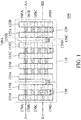
- FIG. 1 shows a semiconductor structure 100 of an integrated circuit (IC) according to an embodiment of the invention.
- the semiconductor structure 100 comprises a radio frequency (RF) circuit 110, a guard ring 120 disposed on the right side of the RF circuit 110, and a guard ring 130 disposed on the left side of the RF circuit 110.
- the RF circuit 110 comprises at least one RF device, and the RF device is a FIN field-effect transistor (FET) formed by a plurality of polys 115A-115D and a plurality of fins 150A-150D.
- the RF circuit 110 comprises a plurality of RF devices, and each RF device is a FIN FET.
- the polys 115A-115D are parallel to each other, and the fins 150A-150D are parallel to each other. Furthermore, the polys 115A-115D are perpendicular to the fins 150A-150D. In some embodiments, the distances D1 between two adjacent polys of the polys 115A-115D are the same. It should be noted that the number of polys and the fins in the RF circuit 110 are determined according to the actual design of the RF devices.
- the guard ring 120 comprises a pair of polys 125A and 125B and a plurality of fins 160A-160D.
- the polys 125A and 125B are parallel to the polys 115A-115D, and the polys 125A and 125B are perpendicular to the fins 160A-160D. Furthermore, the fins 150A-150D of the RF circuit 110 and the fins 160A-160D of the guard ring 120 are disposed on the same row lines, respectively. For example, the fins 150A and 160A are disposed on a first row line, the fins 150B and 160B are disposed on a second row line, the fins 150C and 160C are disposed on a third row line, and the fins 150D and 160D are disposed on a fourth row line.
- the distance D1 between the two adjacent polys of the polys 115A-115D is the same as the distance D2 between the polys 125A and 125B, and the distance D2 between the polys 125A and 125B is the same as the distance D3 between the polys 115D and 125A.
- the guard ring 120 only comprises one pair of polys 125A and 125B, i.e. the number of polys in the guard ring is equal to 2. It should be noted that the number of polys in the RF circuit 110 is greater than the number of polys in the guard ring 120. Moreover, the number of fins (e.g.
- the 160A-160D) in the guard ring 120 is determined according to the number of fins (e.g. 150A-150D) in the RF circuit 110. It should be noted that the conductive type of the fins 150A-150D in the RF circuit 110 is different from the conductive type of the fins 160A-160D in the guard ring 120. In FIG. 1 , the fins 150A-150D of the RF circuit 110 are N+ doped fins, and the fins 160A-160D of the guard ring 120 are P+ doped fins.
- the guard ring 130 comprises a pair of polys 135A and 135B and a plurality of fins 170A-170D.
- the polys 135A and 135B are parallel to the polys 115A-115D, and the polys 135A and 135B are perpendicular to the fins 170A-170D.
- the fins 150A-150D of the RF circuit 110 and the fins 170A-170D of the guard ring 130 are disposed on the same row lines, respectively.
- the guard rings 120 and 130 have the same configuration, and the distance D2 between the polys 135A and 135B is equal to the distance D2 between the polys 125A and 125B.
- the guard ring 130 only comprises the pair of polys 135A and 135B, i.e. the number of polys in the guard ring is equal to 2. It should be noted that the number of polys in the RF circuit 110 is greater than the number of polys in the guard ring 130. Moreover, the number of fins (e.g. 170A-170D) in the guard ring 130 is determined according to the number of fins (e.g. 150A-150D) in the RF circuit 110.
- the lengths of the fins 170A-170D (e.g. from the left side of the poly 135A to the right side of the poly 135B) of the guard ring 130 are equal to the lengths (e.g. from the left side of the poly 125A to the right side of the poly 125B) of the fins 160A-160D of the guard ring 120. Furthermore, the lengths of the fins 170A-170D (e.g. from the left side of the poly 135A to the right side of the poly 135B) of the guard ring 130 are shorter than the lengths (e.g.
- the fins 150A-150D of the RF circuit 110 are N+ doped fins
- the fins 170A-170D of the guard ring 130 are P+ doped fins.
- the guard rings 120 and 130 are coupled together to form a quadrangle, so as to surround (or encircle) the RF circuit 110.
- FIG. 2A shows a sectional view along line A-AA of the semiconductor structure 100 of FIG. 1 .
- a P-type well 220 is disposed on a substrate 210, and the fins 170A, 150A and 160A are disposed on the P-type well 220.
- the fin 170A of the guard ring 130 is separated from the fin 150A of RF circuit 110 by an isolation region 230, such as shallow trench isolation (STI).
- the fin 160A of the guard ring 120 is separated from the fin 150A of RF circuit 110 by an isolation region 230. It should be noted that the isolation region 230 directly contact the fins 170A and 150A, and the isolation region 230 directly contact the fins 160A and 150A.
- STI shallow trench isolation
- no active area or dummy active area is arranged between the guard ring 120 and the RF circuit 110 and between the guard ring 130 and the RF circuit 110.
- three active areas 155A-155C of the fin 150A form the drain/source regions of the same FIN FET, and the active area 175A of the fin 170A and the active area 165A of the FIN 160A form the bulk regions of the same FIN FET.
- the active areas 155A and 155C form the drain regions of the FIN FET
- the active area 155B forms the source region of the FIN FET
- the gate electrode of the FIN FET is coupled to the polys 115B and 115C.
- the active areas 155A and 155C form the source regions of the FIN FET
- the active area 155B forms the drain region of the FIN FET
- the gate electrode of the FIN FET is coupled to the polys 115B and 115C.
- the polys 115A-115D do not overlap the active areas 155A-155C.
- the three active areas 155A-155C form the drain/source regions of the different FIN FETs in the fin 150A.
- the active area 155A forms the drain region of a first FIN FET and the active area 155C forms the drain region of a second FIN FET
- the active area 155B forms the source region of the first and second FIN FETs.
- the gate electrode of the first FIN FET is coupled to the poly 115B
- the gate electrode of the second FIN FET is coupled to the poly 115C.
- the active area 155A forms the source region of the first FIN FET and the active area 155C forms the source region of the second FIN FET
- the active area 155B forms the drain region of the first and second FIN FETs.
- the gate electrode of the first FIN FET is coupled to the poly 115B
- the gate electrode of the second FIN FET is coupled to the poly 115C.
- the active area 175A of the fin 170A and the active area 165A of the FIN 160A form the bulk regions of the first and second FIN FETs, i.e. the bulk regions of the first and second FIN FETs are coupled together.
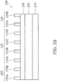
- FIG. 2B shows a sectional view along line B-BB of the semiconductor structure 100 of FIG. 1 .
- the P-type well 220 is disposed on the substrate 210, and an isolation region 230 is disposed on the P-type well 220.
- the depth of the isolation region 230 of FIG. 2B is less than the depth of the isolation region 230 of FIG. 2A .
- the polys 135A-135B, 115A-115D, and 125A-125B have greater depth in FIG. 2B .
- FIG. 3 shows a semiconductor structure 300 of an IC according to another embodiment of the invention.
- the semiconductor structure 300 comprises an RF circuit 310, a guard ring 320 disposed on the right side of the RF circuit 310, and a guard ring 330 disposed on the left side of the RF circuit 310.
- the RF circuit 310 comprises at least one RF device, and the RF device is a FIN FET formed by a plurality of polys 315A-315D and a plurality of fins 350A-350D. As described above, the polys 315A-315D are parallel to each other, and the fins 350A-350D are parallel to each other.
- the polys 315A-315D are perpendicular to the fins 350A-350D.
- the guard rings 320 and 330 have the same configure. Taking the guard ring 320 as an example for description, the guard ring 320 comprises a pair of polys 325A and 325B and a plurality of fins 360A-360D. The polys 325A and 325B are parallel to the polys 315A-315D, and the polys 325A and 325B are perpendicular to the fins 360A-360D. Furthermore, the fins 350A-350D of the RF circuit 310 and the fins 360A-360D of the guard ring 320 are disposed on the same row lines, respectively.
- the fins 350A and 360A are disposed on a first row line
- the fins 350B and 360B are disposed on a second row line
- the fins 350C and 360C are disposed on a third row line
- the fins 350D and 360D are disposed on a fourth row line.
- the guard rings 320 and 330 only comprises the pair of polys 325A and 325B and the pair of polys 335A and 335B, respectively.
- the number of polys in the guard rings 320 and 330 is equal to 2. It should be noted that the number of polys in the RF circuit 310 is greater than the number of polys in the guard rings 320 and 330.
- the number of fins (e.g. 360A-360D and 370A-370D) in the guard rings 320 and 330 are determined according to the number of fins (e.g. 350A-350D) in the RF circuit 310. In some embodiments, the lengths of the fins 370A-370D (e.g.
- the lengths of the fins 370A-370D (e.g. from the left side of the poly 335A to the right side of the poly 335B) of the guard ring 330 are shorter than the lengths (e.g. from the left side of the poly 315A to the right side of the poly 315D) of the fins 350A-350D of the RF circuit 310.
- the conductive type of the fins 350A-350D in the RF circuit 310 is different from the conductive type of the fins 360A-360D in the guard ring 320. Furthermore, the conductive type of the fins 360A-360D in the guard ring 320 and the conductive type of the fins 370A-370D in the guard ring 330 are the same. In FIG. 3 , the fins 350A-350D of the RF circuit 310 are N+ doped fins, and the fins 360A-360D of the guard ring 320 and the fins 370A-370D of the guard ring 330 are P+ doped fins. In some embodiments, the guard rings 320 and 330 are coupled together to form a quadrangle, so as to surround (or encircle) the RF circuit 310.
- the semiconductor structure 300 of FIG. 3 further comprises a dummy poly 340A disposed between the guard ring 330 and the RF circuit 310, and a dummy poly 340B disposed between the guard ring 320 and the RF circuit 310.
- the dummy polys 340A and 340B are arranged parallel to the polys 315A-315D of the RF circuit 310, the polys 325A-325B of the guard ring 320, and the polys 335A-335B of the guard ring 330.
- a plurality of dummy polys 340A are disposed between the guard ring 330 and the RF circuit 310, and a plurality of dummy polys 340B are disposed between the guard ring 330 and the RF circuit 310. Furthermore, the number of dummy polys 340A is equal to that of the dummy polys 340B, so as to obtain a symmetrical layout. As described above, the distances D1 between the polys 315A-315D are the same. It should be noted that the number of polys and the fins in the RF circuit 310 are determined according to the actual design of the RF devices.
- the distance D1 between two adjacent polys of the polys 315A-315D is the same as the distance D2 of the polys 325A and 325B.
- the distance D5 between the poly 315A of the RF circuit 310 and the dummy poly 340A is the same as the distance D4 between the poly 335b of the guard ring 330 and the dummy poly 340A.
- the distances D1, D2, D4 and D5 are equal.
- FIG. 4A shows a sectional view along line C-CC of the semiconductor structure 300 of FIG. 3 .
- a P-type well 420 is disposed on a substrate 410, and the fins 370A, 350A and 360A are disposed on the P-type well 420.
- the fin 370A of the guard ring 330 is separated from the fin 350A of RF circuit 310 by an isolation region 430, such as shallow trench isolation (STI).
- the fin 360A of the guard ring 320 is separated from the fin 350A of RF circuit 310 by an isolation region 430. It should be noted that the isolation 430 directly contact the fins 370A and 350A, and the isolation 430 directly contact the fins 360A and 350A.
- STI shallow trench isolation
- the dummy poly 340A is disposed on the isolation region 430 between the fins 370A and 350A, and the dummy poly 340A directly contacts the isolation region 430.
- the dummy poly 340B is disposed on the isolation region 430 between the fins 360A and 350A, and the dummy poly 340B directly contacts the isolation region 430.
- the active areas are formed in the fin.
- the three active areas 355A-355C of the fin 350A form the drain/source regions of the same FIN FET, and the active area 375A of the fin 370A and the active area 365A of the FIN 360A form the bulk regions of the same FIN FET. If the active areas 355A and 355C form the drain regions of the FIN FET, the active area 355B forms the source region of the FIN FET, and the gate electrode of the FIN FET is coupled to the polys 315B and 315C.
- the active areas 355A and 355C form the source regions of the FIN FET
- the active area 355B forms the drain region of the FIN FET
- the gate electrode of the FIN FET is coupled to the polys 315B and 315C.
- the polys 315A-315D do not overlap the active areas 355A-355C.
- the three active areas 355A-355C form the drain/source regions of the different FIN FETs in the fin 350A.
- the active area 355A forms the drain region of a first FIN FET and the active area 355C forms the drain region of a second FIN FET
- the active area 355B forms the source region of the first and second FIN FETs.
- the gate electrode of the first FIN FET is coupled to the poly 315B
- the gate electrode of the second FIN FET is coupled to the poly 315C.
- the active area 355A forms the source region of the first FIN FET and the active area 355C forms the source region of the second FIN FET
- the active area 355B forms the drain region of the first and second FIN FETs.
- the gate electrode of the first FIN FET is coupled to the poly 315B
- the gate electrode of the second FIN FET is coupled to the poly 315C.
- the active area 375A of the fin 370A and the active area 365A of the FIN 360A form the bulk regions of the first and second FIN FETs, i.e. the bulk regions of the first and second FIN FETs are coupled together.
- FIG. 4B shows a sectional view along line D-DD of the semiconductor structure 300 of FIG. 3 .
- the P-type well 420 is disposed on the substrate 410, and an isolation region 430 is disposed on the P-type well 420.
- the depth of the isolation region 430 of FIG. 4B is less than the depth of the isolation region 430 of FIG. 4A .
- the polys 335A-335B, 315A-315D, and 325A-325B, and the dummy polys 340A-340B have greater depth in FIG. 4B .
- the guard rings by arranging the guard rings on both opposite sides of the RF circuit, noise or interference can be decreased for the RF circuit. Furthermore, arranging the guard ring next to the RF circuit, i.e., the fins of the guard ring and the fins of the RF circuit are separated by the isolation regions, the area of the semiconductor structure is decreased, and thus manufacturing cost of the IC is decreased.
Landscapes
- Semiconductor Integrated Circuits (AREA)
- Metal-Oxide And Bipolar Metal-Oxide Semiconductor Integrated Circuits (AREA)
- Engineering & Computer Science (AREA)
- General Engineering & Computer Science (AREA)
Abstract
Description
- This application claims the benefit of
U.S. Provisional Application No. 62/339,123, filed on May 20, 2016 U.S. Provisional Application No. 62/382,288, filed on September 1, 2016 - The invention relates to a semiconductor structure, and more particularly to a semiconductor structure of a guard ring for a radio frequency (RF) device.
- Semiconductor device manufacturers are tasked to deliver products that perform with an expected level of quality. In an integrated circuit (IC), one circuit or device will introduce noise that interferes with the operation of other circuits or devices in the IC. This introduction of noise often degrades the performance of the IC.
- Guard rings are used as isolation regions between devices or circuits within an IC. Guard rings surround the devices or circuits of the IC in order to reduce interference or noise between adjacent devices or circuits. Guard rings are more important for high-frequency circuits (such as radio frequency (RF) circuits) that are susceptible to interference and noise.
- Semiconductor structures are provided. An embodiment of a semiconductor structure is provided. The semiconductor structure comprises a semiconductor substrate, a well region on the semiconductor substrate, a radio frequency (RF) circuit, a first guard ring adjacent to the RF circuit, and a first isolation region directly disposed between the RF circuit and the first guard ring. The well region has a first conductive type. The RF circuit comprises at least one FIN field-effect transistor having a plurality of first fins and a plurality of first polys on the well region, wherein the first polys are perpendicular to the first fins. The first guard ring comprises a plurality of second fins and a pair of second polys on the well region, wherein the second polys are perpendicular to the second fins. The first fins are arranged parallel to the second fins, and the first fins are separated from the second fins by the first isolation region. The semiconductor structure may include one or more of the following features:
- The first polys may be arranged parallel to the second polys.
- The number of first fins may be equal to the number of second fins.
- Each of the first fins may comprise a plurality of first active areas having a second conductive type, and each of the second fins may comprise a second active area having the first conductive type.
- The semiconductor structure may further comprise: a dummy poly on the first isolation region, wherein the first and second polys and the dummy poly are arranged parallel to each other.
- A distance between the dummy poly and one of the first polys may be equal to a distance between the dummy poly and the second poly adjacent to the one of the first polys.
- The semiconductor structure may further comprise: a second guard ring adjacent to the RF circuit, comprising a plurality of third fins and a pair of third polys on the well region, wherein the third polys are perpendicular to the third fins; and a second isolation region directly disposed between the RF circuit and the second guard ring, wherein the number of third fins is equal to the number of second fins, wherein length of each of the third fins is equal to that of the second fin, and the length of each of the third fins is shorter than that of the first fin.
- The first guard ring may form a bulk region of the FIN field-effect transistor.
- The number of first polys may be greater than the number of second polys.
- Furthermore, another embodiment of a semiconductor structure is provided. The semiconductor substrate comprises a semiconductor substrate, a well region on the semiconductor substrate, a radio frequency (RF) circuit, a pair of guard rings disposed on both opposite sides of the RF circuit, a first isolation region on the well region, and a second isolation region on the well region. The well region has a first conductive type. The RF circuit comprises at least one FIN field-effect transistor having a plurality of first fins and a plurality of first polys on the well region, wherein the first fins have a second conductive type, and the first polys are perpendicular to the first fins. Each of the guard rings comprises a plurality of second fins and a pair of second polys on the well region, wherein the second fins have the first conductive type, and the second polys are perpendicular to the second fins. The first isolation region is directly disposed between the RF circuit and one of the guard rings. The second isolation region is directly disposed between the RF circuit and the other guard ring. The first fins are arranged parallel to the second fins, and the first fins are separated from the second fins by the first and second isolation regions. The semiconductor structure may include one or more of the following features:
- Each of the first and second isolation regions may directly contact the first fins and the second fins.
- The distance between the two adjacent first polys may be equal to distance between the two adjacent second polys.
- The number of first fins may be equal to the number of second fins in each of the guard rings.
- The number of first polys may be greater than the number of second polys in each of the guard rings.
- The semiconductor structure may further comprise: a first dummy poly on the first isolation region; and a second dummy poly on the second isolation region, wherein the first and second dummy polys are arranged parallel to the first and second polys.
- The first and second dummy polys may overlap the first and second isolation regions, respectively.
- A distance between the first dummy poly and one of the first polys adjacent to the first isolation region may be equal to a distance between the first dummy poly and the second poly adjacent to the first isolation region, and a distance between the second dummy poly and one of the first polys adjacent to the second isolation region may be equal to a distance between the second dummy poly and the second poly adjacent to the second isolation region.
- Each of the first fins mays comprise a plurality of first active areas having the second conductive type, and the first active areas may form drain regions and source regions of the FIN field-effect transistor.
- Each of the second fins may comprise a second active area having the first conductive type, and the second active area may form a bulk region of the FIN field-effect transistor.
- A length of each of the second fins may be shorter than that of the first fin.
- A detailed description is given in the following embodiments with reference to the accompanying drawings.
- The invention can be more fully understood by reading the subsequent detailed description and examples with references made to the accompanying drawings, wherein:
-
FIG. 1 shows a semiconductor structure of an integrated circuit (IC) according to an embodiment of the invention; -
FIG. 2A shows a sectional view along line A-AA of the semiconductor structure ofFIG. 1 ; -
FIG. 2B shows a sectional view along line B-BB of the semiconductor structure ofFIG. 1 ; -
FIG. 3 shows a semiconductor structure of an IC according to another embodiment of the invention; -
FIG. 4A shows a sectional view along line C-CC of the semiconductor structure ofFIG. 3 ; and -
FIG. 4B shows a sectional view along line D-DD of the semiconductor structure ofFIG. 3 . - The following description is of the best-contemplated mode of carrying out the invention. This description is made for the purpose of illustrating the general principles of the invention and should not be taken in a limiting sense. The scope of the invention is best determined by reference to the appended claims.
-
FIG. 1 shows asemiconductor structure 100 of an integrated circuit (IC) according to an embodiment of the invention. Thesemiconductor structure 100 comprises a radio frequency (RF)circuit 110, aguard ring 120 disposed on the right side of theRF circuit 110, and aguard ring 130 disposed on the left side of theRF circuit 110. In theRF circuit 110, theRF circuit 110 comprises at least one RF device, and the RF device is a FIN field-effect transistor (FET) formed by a plurality ofpolys 115A-115D and a plurality offins 150A-150D. In some embodiments, theRF circuit 110 comprises a plurality of RF devices, and each RF device is a FIN FET. In theRF circuit 110, thepolys 115A-115D are parallel to each other, and thefins 150A-150D are parallel to each other. Furthermore, thepolys 115A-115D are perpendicular to thefins 150A-150D. In some embodiments, the distances D1 between two adjacent polys of thepolys 115A-115D are the same. It should be noted that the number of polys and the fins in theRF circuit 110 are determined according to the actual design of the RF devices. Theguard ring 120 comprises a pair ofpolys fins 160A-160D. Thepolys polys 115A-115D, and thepolys fins 160A-160D. Furthermore, thefins 150A-150D of theRF circuit 110 and thefins 160A-160D of theguard ring 120 are disposed on the same row lines, respectively. For example, thefins fins fins fins polys 115A-115D is the same as the distance D2 between thepolys polys polys semiconductor structure 100, theguard ring 120 only comprises one pair ofpolys RF circuit 110 is greater than the number of polys in theguard ring 120. Moreover, the number of fins (e.g. 160A-160D) in theguard ring 120 is determined according to the number of fins (e.g. 150A-150D) in theRF circuit 110. It should be noted that the conductive type of thefins 150A-150D in theRF circuit 110 is different from the conductive type of thefins 160A-160D in theguard ring 120. InFIG. 1 , thefins 150A-150D of theRF circuit 110 are N+ doped fins, and thefins 160A-160D of theguard ring 120 are P+ doped fins. - Similarly, the
guard ring 130 comprises a pair ofpolys fins 170A-170D. Thepolys polys 115A-115D, and thepolys fins 170A-170D. As described above, thefins 150A-150D of theRF circuit 110 and thefins 170A-170D of theguard ring 130 are disposed on the same row lines, respectively. In some embodiments, the guard rings 120 and 130 have the same configuration, and the distance D2 between thepolys polys polys polys semiconductor structure 100, theguard ring 130 only comprises the pair ofpolys RF circuit 110 is greater than the number of polys in theguard ring 130. Moreover, the number of fins (e.g. 170A-170D) in theguard ring 130 is determined according to the number of fins (e.g. 150A-150D) in theRF circuit 110. In some embodiments, the lengths of thefins 170A-170D (e.g. from the left side of thepoly 135A to the right side of the poly 135B) of theguard ring 130 are equal to the lengths (e.g. from the left side of thepoly 125A to the right side of the poly 125B) of thefins 160A-160D of theguard ring 120. Furthermore, the lengths of thefins 170A-170D (e.g. from the left side of thepoly 135A to the right side of the poly 135B) of theguard ring 130 are shorter than the lengths (e.g. from the left side of thepoly 115A to the right side of thepoly 115D) of thefins 150A-150D of theRF circuit 110. Moreover, thefins 150A-150D of theRF circuit 110 are N+ doped fins, and thefins 170A-170D of theguard ring 130 are P+ doped fins. In some embodiments, the guard rings 120 and 130 are coupled together to form a quadrangle, so as to surround (or encircle) theRF circuit 110. -
FIG. 2A shows a sectional view along line A-AA of thesemiconductor structure 100 ofFIG. 1 . A P-type well 220 is disposed on asubstrate 210, and thefins type well 220. Thefin 170A of theguard ring 130 is separated from thefin 150A ofRF circuit 110 by anisolation region 230, such as shallow trench isolation (STI). Furthermore, thefin 160A of theguard ring 120 is separated from thefin 150A ofRF circuit 110 by anisolation region 230. It should be noted that theisolation region 230 directly contact thefins isolation region 230 directly contact thefins guard ring 120 and theRF circuit 110 and between theguard ring 130 and theRF circuit 110. In one embodiment, threeactive areas 155A-155C of thefin 150A form the drain/source regions of the same FIN FET, and theactive area 175A of thefin 170A and theactive area 165A of theFIN 160A form the bulk regions of the same FIN FET. For example, if theactive areas active area 155B forms the source region of the FIN FET, and the gate electrode of the FIN FET is coupled to thepolys active areas active area 155B forms the drain region of the FIN FET, and the gate electrode of the FIN FET is coupled to thepolys polys 115A-115D do not overlap theactive areas 155A-155C. In some embodiments, the threeactive areas 155A-155C form the drain/source regions of the different FIN FETs in thefin 150A. For example, if theactive area 155A forms the drain region of a first FIN FET and theactive area 155C forms the drain region of a second FIN FET, theactive area 155B forms the source region of the first and second FIN FETs. Furthermore, the gate electrode of the first FIN FET is coupled to thepoly 115B, and the gate electrode of the second FIN FET is coupled to thepoly 115C. Conversely, if theactive area 155A forms the source region of the first FIN FET and theactive area 155C forms the source region of the second FIN FET, theactive area 155B forms the drain region of the first and second FIN FETs. Furthermore, the gate electrode of the first FIN FET is coupled to thepoly 115B, and the gate electrode of the second FIN FET is coupled to thepoly 115C. Moreover, theactive area 175A of thefin 170A and theactive area 165A of theFIN 160A form the bulk regions of the first and second FIN FETs, i.e. the bulk regions of the first and second FIN FETs are coupled together. -
FIG. 2B shows a sectional view along line B-BB of thesemiconductor structure 100 ofFIG. 1 . Similarly, the P-type well 220 is disposed on thesubstrate 210, and anisolation region 230 is disposed on the P-type well 220. Furthermore, the depth of theisolation region 230 ofFIG. 2B is less than the depth of theisolation region 230 ofFIG. 2A . Compared withFIG. 2A , due to there being no fin in line B-BB, thepolys 135A-135B, 115A-115D, and 125A-125B have greater depth inFIG. 2B . -
FIG. 3 shows asemiconductor structure 300 of an IC according to another embodiment of the invention. Thesemiconductor structure 300 comprises anRF circuit 310, aguard ring 320 disposed on the right side of theRF circuit 310, and aguard ring 330 disposed on the left side of theRF circuit 310. In theRF circuit 310, theRF circuit 310 comprises at least one RF device, and the RF device is a FIN FET formed by a plurality ofpolys 315A-315D and a plurality offins 350A-350D. As described above, thepolys 315A-315D are parallel to each other, and thefins 350A-350D are parallel to each other. Furthermore, thepolys 315A-315D are perpendicular to thefins 350A-350D. As described above, the guard rings 320 and 330 have the same configure. Taking theguard ring 320 as an example for description, theguard ring 320 comprises a pair ofpolys fins 360A-360D. Thepolys polys 315A-315D, and thepolys fins 360A-360D. Furthermore, thefins 350A-350D of theRF circuit 310 and thefins 360A-360D of theguard ring 320 are disposed on the same row lines, respectively. For example, thefins fins fins fins - In order to reduce the area of the
semiconductor structure 300, the guard rings 320 and 330 only comprises the pair ofpolys polys RF circuit 310 is greater than the number of polys in the guard rings 320 and 330. Moreover, the number of fins (e.g. 360A-360D and 370A-370D) in the guard rings 320 and 330 are determined according to the number of fins (e.g. 350A-350D) in theRF circuit 310. In some embodiments, the lengths of thefins 370A-370D (e.g. from the left side of thepoly 335A to the right side of the poly 335B) of theguard ring 330 are equal to the lengths (e.g. from the left side of thepoly 325A to the right side of the poly 325B) of thefins 360A-360D of theguard ring 320. Furthermore, the lengths of thefins 370A-370D (e.g. from the left side of thepoly 335A to the right side of the poly 335B) of theguard ring 330 are shorter than the lengths (e.g. from the left side of thepoly 315A to the right side of thepoly 315D) of thefins 350A-350D of theRF circuit 310. It should be noted that the conductive type of thefins 350A-350D in theRF circuit 310 is different from the conductive type of thefins 360A-360D in theguard ring 320. Furthermore, the conductive type of thefins 360A-360D in theguard ring 320 and the conductive type of thefins 370A-370D in theguard ring 330 are the same. InFIG. 3 , thefins 350A-350D of theRF circuit 310 are N+ doped fins, and thefins 360A-360D of theguard ring 320 and thefins 370A-370D of theguard ring 330 are P+ doped fins. In some embodiments, the guard rings 320 and 330 are coupled together to form a quadrangle, so as to surround (or encircle) theRF circuit 310. - Compared with the
semiconductor structure 100 ofFIG. 1 , thesemiconductor structure 300 ofFIG. 3 further comprises adummy poly 340A disposed between theguard ring 330 and theRF circuit 310, and adummy poly 340B disposed between theguard ring 320 and theRF circuit 310. Thedummy polys polys 315A-315D of theRF circuit 310, thepolys 325A-325B of theguard ring 320, and thepolys 335A-335B of theguard ring 330. In some embodiments, a plurality ofdummy polys 340A are disposed between theguard ring 330 and theRF circuit 310, and a plurality ofdummy polys 340B are disposed between theguard ring 330 and theRF circuit 310. Furthermore, the number ofdummy polys 340A is equal to that of thedummy polys 340B, so as to obtain a symmetrical layout. As described above, the distances D1 between thepolys 315A-315D are the same. It should be noted that the number of polys and the fins in theRF circuit 310 are determined according to the actual design of the RF devices. Furthermore, the distance D1 between two adjacent polys of thepolys 315A-315D is the same as the distance D2 of thepolys RF circuit 310 and thedummy poly 340A is the same as the distance D4 between the poly 335b of theguard ring 330 and thedummy poly 340A. In some embodiments, the distances D1, D2, D4 and D5 are equal. -
FIG. 4A shows a sectional view along line C-CC of thesemiconductor structure 300 ofFIG. 3 . A P-type well 420 is disposed on asubstrate 410, and thefins type well 420. Thefin 370A of theguard ring 330 is separated from thefin 350A ofRF circuit 310 by anisolation region 430, such as shallow trench isolation (STI). Furthermore, thefin 360A of theguard ring 320 is separated from thefin 350A ofRF circuit 310 by anisolation region 430. It should be noted that theisolation 430 directly contact thefins isolation 430 directly contact thefins guard ring 320 and theRF circuit 310 and between theguard ring 330 and theRF circuit 310. Furthermore, thedummy poly 340A is disposed on theisolation region 430 between thefins dummy poly 340A directly contacts theisolation region 430. Similarly, thedummy poly 340B is disposed on theisolation region 430 between thefins dummy poly 340B directly contacts theisolation region 430. As described above, the active areas are formed in the fin. For example, the threeactive areas 355A-355C of thefin 350A form the drain/source regions of the same FIN FET, and theactive area 375A of thefin 370A and theactive area 365A of theFIN 360A form the bulk regions of the same FIN FET. If theactive areas active area 355B forms the source region of the FIN FET, and the gate electrode of the FIN FET is coupled to thepolys active areas active area 355B forms the drain region of the FIN FET, and the gate electrode of the FIN FET is coupled to thepolys polys 315A-315D do not overlap theactive areas 355A-355C. In some embodiments, the threeactive areas 355A-355C form the drain/source regions of the different FIN FETs in thefin 350A. For example, if theactive area 355A forms the drain region of a first FIN FET and theactive area 355C forms the drain region of a second FIN FET, theactive area 355B forms the source region of the first and second FIN FETs. Furthermore, the gate electrode of the first FIN FET is coupled to thepoly 315B, and the gate electrode of the second FIN FET is coupled to thepoly 315C. Conversely, if theactive area 355A forms the source region of the first FIN FET and theactive area 355C forms the source region of the second FIN FET, theactive area 355B forms the drain region of the first and second FIN FETs. Furthermore, the gate electrode of the first FIN FET is coupled to thepoly 315B, and the gate electrode of the second FIN FET is coupled to thepoly 315C. Moreover, theactive area 375A of thefin 370A and theactive area 365A of theFIN 360A form the bulk regions of the first and second FIN FETs, i.e. the bulk regions of the first and second FIN FETs are coupled together. -
FIG. 4B shows a sectional view along line D-DD of thesemiconductor structure 300 ofFIG. 3 . Similarly, the P-type well 420 is disposed on thesubstrate 410, and anisolation region 430 is disposed on the P-type well 420. Furthermore, the depth of theisolation region 430 ofFIG. 4B is less than the depth of theisolation region 430 ofFIG. 4A . Compared withFIG. 4A , due to there being no fin in line D-DD, thepolys 335A-335B, 315A-315D, and 325A-325B, and thedummy polys 340A-340B have greater depth inFIG. 4B . - According to the embodiments, by arranging the guard rings on both opposite sides of the RF circuit, noise or interference can be decreased for the RF circuit. Furthermore, arranging the guard ring next to the RF circuit, i.e., the fins of the guard ring and the fins of the RF circuit are separated by the isolation regions, the area of the semiconductor structure is decreased, and thus manufacturing cost of the IC is decreased.
- While the invention has been described by way of example and in terms of the preferred embodiments, it is to be understood that the invention is not limited to the disclosed embodiments. On the contrary, it is intended to cover various modifications and similar arrangements (as would be apparent to those skilled in the art). Therefore, the scope of the appended claims should be accorded the broadest interpretation so as to encompass all such modifications and similar arrangements.
Claims (15)
- A semiconductor structure, comprising:a semiconductor substrate;a well region on the semiconductor substrate, having a first conductive type;a radio frequency (RF) circuit, comprising at least one FIN field-effect transistor having a plurality of first fins and a plurality of first polys on the well region, wherein the first polys are perpendicular to the first fins;a first guard ring adjacent to the RF circuit, comprising a plurality of second fins and a pair of second polys on the well region, wherein the second polys are perpendicular to the second fins; anda first isolation region directly disposed between the RF circuit and the first guard ring,wherein the first fins are arranged parallel to the second fins, and the first fins are separated from the second fins by the first isolation region.
- The semiconductor structure as claimed in claim 1, wherein the first polys are arranged parallel to the second polys.
- The semiconductor structure as claimed in claim 1 or 2, wherein the number of first fins is equal to the number of second fins.
- The semiconductor structure as claimed in one of the preceding claims, wherein each of the first fins comprises a plurality of first active areas having a second conductive type, and each of the second fins comprises a second active area having the first conductive type.
- The semiconductor structure as claimed in one of the preceding claims, further comprising:a dummy poly on the first isolation region,wherein the first and second polys and the dummy poly are arranged parallel to each other.
- The semiconductor structure as claimed in one of the preceding claims, further comprising:a second guard ring adjacent to the RF circuit, comprising a plurality of third fins and a pair of third polys on the well region, wherein the third polys are perpendicular to the third fins; anda second isolation region directly disposed between the RF circuit and the second guard ring,wherein the number of third fins is equal to the number of second fins,wherein length of each of the third fins is equal to that of the second fin, and the length of each of the third fins is shorter than that of the first fin.
- The semiconductor structure as claimed in one of the preceding claims, wherein the first guard ring forms a bulk region of the FIN field-effect transistor.
- The semiconductor structure as claimed in one of the preceding claims, wherein the number of first polys is greater than the number of second polys.
- A semiconductor structure as claimed in one of the preceding claims, comprising:a pair of guard rings disposed on both opposite sides of the RF circuit, the pair of guard rings including the first guard ring, wherein each of the guard rings comprises a plurality of second fins and a pair of second polys on the well region, wherein the second fins have the first conductive type, and the second polys are perpendicular to the second fins;the first isolation region on the well region, wherein the first isolation region is directly disposed between the RF circuit and one of the guard rings; anda second isolation region on the well region, wherein the second isolation region is directly disposed between the RF circuit and the other guard ring.wherein the first fins are separated from the second fins by the first and second isolation regions.
- The semiconductor structure as claimed in claim 9, wherein each of the first and second isolation regions directly contacts the first fins and the second fins.
- The semiconductor structure as claimed in claim 9 or 10, wherein distance between the two adjacent first polys is equal to distance between the two adjacent second polys.
- The semiconductor structure as claimed in one of claims 9 10 11, further comprising:a first dummy poly on the first isolation region; anda second dummy poly on the second isolation region,wherein the first and second dummy polys are arranged parallel to the first and second polys; andwherein the first and second dummy polys overlap the first and second isolation regions, respectively.
- The semiconductor structure as claimed in claim 12, wherein a distance between the first dummy poly and one of the first polys adjacent to the first isolation region is equal to a distance between the first dummy poly and the second poly adjacent to the first isolation region, and a distance between the second dummy poly and one of the first polys adjacent to the second isolation region is equal to a distance between the second dummy poly and the second poly adjacent to the second isolation region.
- The semiconductor structure as claimed in one of claims 10, wherein each of the first fins comprises a plurality of first active areas having the second conductive type, and the first active areas form drain regions and source regions of the FIN field-effect transistor; and/or
wherein each of the second fins comprises a second active area having the first conductive type, and the second active area forms a bulk region of the FIN field-effect transistor. - The semiconductor structure as claimed in one of claims 9 10 14, wherein length of each of the second fins is shorter than that of the first fin.
Applications Claiming Priority (3)
| Application Number | Priority Date | Filing Date | Title |
|---|---|---|---|
| US201662339123P | 2016-05-20 | 2016-05-20 | |
| US201662382288P | 2016-09-01 | 2016-09-01 | |
| US15/493,199 US9978751B2 (en) | 2016-05-20 | 2017-04-21 | Semiconductor structure |
Publications (2)
| Publication Number | Publication Date |
|---|---|
| EP3246951A1 true EP3246951A1 (en) | 2017-11-22 |
| EP3246951B1 EP3246951B1 (en) | 2021-07-07 |
Family
ID=58671438
Family Applications (1)
| Application Number | Title | Priority Date | Filing Date |
|---|---|---|---|
| EP17169363.3A Active EP3246951B1 (en) | 2016-05-20 | 2017-05-04 | Semiconductor structure |
Country Status (4)
| Country | Link |
|---|---|
| US (1) | US9978751B2 (en) |
| EP (1) | EP3246951B1 (en) |
| CN (1) | CN107403801B (en) |
| TW (1) | TWI644426B (en) |
Families Citing this family (6)
| Publication number | Priority date | Publication date | Assignee | Title |
|---|---|---|---|---|
| US9978751B2 (en) * | 2016-05-20 | 2018-05-22 | Mediatek Inc. | Semiconductor structure |
| JP6841161B2 (en) * | 2017-05-25 | 2021-03-10 | 株式会社ソシオネクスト | Semiconductor device |
| US10923572B2 (en) * | 2018-09-28 | 2021-02-16 | Taiwan Semiconductor Manufacturing Company Ltd. | Heat sink layout designs for advanced FinFET integrated circuits |
| US11468221B2 (en) * | 2019-05-10 | 2022-10-11 | Samsung Electronics Co.. Ltd. | Methods for VFET cell placement and cell architecture |
| EP4138129A4 (en) * | 2020-04-30 | 2023-06-07 | Huawei Technologies Co., Ltd. | INTEGRATED CIRCUIT |
| US11658223B2 (en) | 2020-10-19 | 2023-05-23 | United Microelectronics Corp. | Semiconductor structure |
Citations (5)
| Publication number | Priority date | Publication date | Assignee | Title |
|---|---|---|---|---|
| US20130200449A1 (en) * | 2012-02-07 | 2013-08-08 | Taiwan Semiconductor Manufacturing Company, Ltd. | Finfet structure with novel edge fins |
| US20140306296A1 (en) * | 2013-04-10 | 2014-10-16 | Chan-Hee Jeon | Semiconductor device and method for fabricating the same |
| US20140367780A1 (en) * | 2013-06-18 | 2014-12-18 | United Microelectronics Corp. | Semiconductor integrated device |
| US20160013187A1 (en) * | 2014-07-09 | 2016-01-14 | Semiconductor Manufacturing International (Shanghai) Corporation | Semiconductor device and electronic apparatus including the same |
| EP3136444A1 (en) * | 2015-08-27 | 2017-03-01 | Altera Corporation | Integrated circuits with guard ring structures for nonplanar transistor devices |
Family Cites Families (6)
| Publication number | Priority date | Publication date | Assignee | Title |
|---|---|---|---|---|
| US8680587B2 (en) * | 2011-09-11 | 2014-03-25 | Cree, Inc. | Schottky diode |
| US8723225B2 (en) * | 2012-10-04 | 2014-05-13 | Taiwan Semiconductor Manufacturing Company, Ltd. | Guard rings on fin structures |
| CN110047933B (en) * | 2013-09-25 | 2022-11-08 | 太浩研究有限公司 | Isolation well doped with solid state diffusion source for FINFET architecture |
| US9324827B1 (en) * | 2014-10-28 | 2016-04-26 | Globalfoundries Inc. | Non-planar schottky diode and method of fabrication |
| CN107104137B (en) * | 2016-02-22 | 2021-11-02 | 联华电子股份有限公司 | Fin transistor element |
| US9978751B2 (en) * | 2016-05-20 | 2018-05-22 | Mediatek Inc. | Semiconductor structure |
-
2017
- 2017-04-21 US US15/493,199 patent/US9978751B2/en active Active
- 2017-05-04 EP EP17169363.3A patent/EP3246951B1/en active Active
- 2017-05-10 CN CN201710324769.2A patent/CN107403801B/en active Active
- 2017-05-19 TW TW106116619A patent/TWI644426B/en not_active IP Right Cessation
Patent Citations (5)
| Publication number | Priority date | Publication date | Assignee | Title |
|---|---|---|---|---|
| US20130200449A1 (en) * | 2012-02-07 | 2013-08-08 | Taiwan Semiconductor Manufacturing Company, Ltd. | Finfet structure with novel edge fins |
| US20140306296A1 (en) * | 2013-04-10 | 2014-10-16 | Chan-Hee Jeon | Semiconductor device and method for fabricating the same |
| US20140367780A1 (en) * | 2013-06-18 | 2014-12-18 | United Microelectronics Corp. | Semiconductor integrated device |
| US20160013187A1 (en) * | 2014-07-09 | 2016-01-14 | Semiconductor Manufacturing International (Shanghai) Corporation | Semiconductor device and electronic apparatus including the same |
| EP3136444A1 (en) * | 2015-08-27 | 2017-03-01 | Altera Corporation | Integrated circuits with guard ring structures for nonplanar transistor devices |
Also Published As
| Publication number | Publication date |
|---|---|
| TW201807821A (en) | 2018-03-01 |
| CN107403801B (en) | 2020-03-31 |
| US20170338231A1 (en) | 2017-11-23 |
| EP3246951B1 (en) | 2021-07-07 |
| TWI644426B (en) | 2018-12-11 |
| US9978751B2 (en) | 2018-05-22 |
| CN107403801A (en) | 2017-11-28 |
Similar Documents
| Publication | Publication Date | Title |
|---|---|---|
| EP3246951B1 (en) | Semiconductor structure | |
| US12489036B2 (en) | Field-effect transistors with interleaved finger configuration | |
| US20120161285A1 (en) | Reducing High-Frequency Signal Loss in Substrates | |
| US11973115B2 (en) | Methods related to switch body connections to achieve soft breakdown | |
| US10944008B2 (en) | Low noise amplifier transistors with decreased noise figure and leakage in silicon-on-insulator technology | |
| US20170125300A1 (en) | Method of fabricating semiconductor | |
| US9595523B2 (en) | Semiconductor integrated circuit devices | |
| US20200381433A1 (en) | Semiconductor cell structure and forming method thereof | |
| EP2965380A1 (en) | Optimizing isolation and insertion loss of a radio frequency single-pole-double-throw switch | |
| US20250142947A1 (en) | Integrated circuit device including metal-oxide semiconductor transistors | |
| CN113872581A (en) | RF switch | |
| US11990507B2 (en) | High voltage transistor structure | |
| US10141256B2 (en) | Semiconductor device and layout design thereof | |
| US9691666B2 (en) | Layout architecture for performance improvement | |
| US20160005813A1 (en) | Fin structures and methods of manfacturing the fin structures, and fin transistors having the fin structures and methods of manufacturing the fin transistors | |
| US20050073366A1 (en) | Dual gate cascade amplifier | |
| US9640629B1 (en) | Semiconductor device and method of manufacturing the same | |
| TW202312488A (en) | Semiconductor structure |
Legal Events
| Date | Code | Title | Description |
|---|---|---|---|
| PUAI | Public reference made under article 153(3) epc to a published international application that has entered the european phase |
Free format text: ORIGINAL CODE: 0009012 |
|
| STAA | Information on the status of an ep patent application or granted ep patent |
Free format text: STATUS: THE APPLICATION HAS BEEN PUBLISHED |
|
| AK | Designated contracting states |
Kind code of ref document: A1 Designated state(s): AL AT BE BG CH CY CZ DE DK EE ES FI FR GB GR HR HU IE IS IT LI LT LU LV MC MK MT NL NO PL PT RO RS SE SI SK SM TR |
|
| AX | Request for extension of the european patent |
Extension state: BA ME |
|
| STAA | Information on the status of an ep patent application or granted ep patent |
Free format text: STATUS: REQUEST FOR EXAMINATION WAS MADE |
|
| 17P | Request for examination filed |
Effective date: 20180511 |
|
| RBV | Designated contracting states (corrected) |
Designated state(s): AL AT BE BG CH CY CZ DE DK EE ES FI FR GB GR HR HU IE IS IT LI LT LU LV MC MK MT NL NO PL PT RO RS SE SI SK SM TR |
|
| STAA | Information on the status of an ep patent application or granted ep patent |
Free format text: STATUS: EXAMINATION IS IN PROGRESS |
|
| 17Q | First examination report despatched |
Effective date: 20200504 |
|
| GRAP | Despatch of communication of intention to grant a patent |
Free format text: ORIGINAL CODE: EPIDOSNIGR1 |
|
| STAA | Information on the status of an ep patent application or granted ep patent |
Free format text: STATUS: GRANT OF PATENT IS INTENDED |
|
| INTG | Intention to grant announced |
Effective date: 20201201 |
|
| GRAS | Grant fee paid |
Free format text: ORIGINAL CODE: EPIDOSNIGR3 |
|
| RAP3 | Party data changed (applicant data changed or rights of an application transferred) |
Owner name: MEDIATEK INC. |
|
| GRAA | (expected) grant |
Free format text: ORIGINAL CODE: 0009210 |
|
| STAA | Information on the status of an ep patent application or granted ep patent |
Free format text: STATUS: THE PATENT HAS BEEN GRANTED |
|
| AK | Designated contracting states |
Kind code of ref document: B1 Designated state(s): AL AT BE BG CH CY CZ DE DK EE ES FI FR GB GR HR HU IE IS IT LI LT LU LV MC MK MT NL NO PL PT RO RS SE SI SK SM TR |
|
| REG | Reference to a national code |
Ref country code: GB Ref legal event code: FG4D |
|
| REG | Reference to a national code |
Ref country code: AT Ref legal event code: REF Ref document number: 1409422 Country of ref document: AT Kind code of ref document: T Effective date: 20210715 |
|
| REG | Reference to a national code |
Ref country code: DE Ref legal event code: R096 Ref document number: 602017041520 Country of ref document: DE |
|
| REG | Reference to a national code |
Ref country code: IE Ref legal event code: FG4D |
|
| REG | Reference to a national code |
Ref country code: LT Ref legal event code: MG9D |
|
| REG | Reference to a national code |
Ref country code: NL Ref legal event code: MP Effective date: 20210707 |
|
| REG | Reference to a national code |
Ref country code: AT Ref legal event code: MK05 Ref document number: 1409422 Country of ref document: AT Kind code of ref document: T Effective date: 20210707 |
|
| PG25 | Lapsed in a contracting state [announced via postgrant information from national office to epo] |
Ref country code: RS Free format text: LAPSE BECAUSE OF FAILURE TO SUBMIT A TRANSLATION OF THE DESCRIPTION OR TO PAY THE FEE WITHIN THE PRESCRIBED TIME-LIMIT Effective date: 20210707 Ref country code: SE Free format text: LAPSE BECAUSE OF FAILURE TO SUBMIT A TRANSLATION OF THE DESCRIPTION OR TO PAY THE FEE WITHIN THE PRESCRIBED TIME-LIMIT Effective date: 20210707 Ref country code: FI Free format text: LAPSE BECAUSE OF FAILURE TO SUBMIT A TRANSLATION OF THE DESCRIPTION OR TO PAY THE FEE WITHIN THE PRESCRIBED TIME-LIMIT Effective date: 20210707 Ref country code: ES Free format text: LAPSE BECAUSE OF FAILURE TO SUBMIT A TRANSLATION OF THE DESCRIPTION OR TO PAY THE FEE WITHIN THE PRESCRIBED TIME-LIMIT Effective date: 20210707 Ref country code: HR Free format text: LAPSE BECAUSE OF FAILURE TO SUBMIT A TRANSLATION OF THE DESCRIPTION OR TO PAY THE FEE WITHIN THE PRESCRIBED TIME-LIMIT Effective date: 20210707 Ref country code: PT Free format text: LAPSE BECAUSE OF FAILURE TO SUBMIT A TRANSLATION OF THE DESCRIPTION OR TO PAY THE FEE WITHIN THE PRESCRIBED TIME-LIMIT Effective date: 20211108 Ref country code: NL Free format text: LAPSE BECAUSE OF FAILURE TO SUBMIT A TRANSLATION OF THE DESCRIPTION OR TO PAY THE FEE WITHIN THE PRESCRIBED TIME-LIMIT Effective date: 20210707 Ref country code: NO Free format text: LAPSE BECAUSE OF FAILURE TO SUBMIT A TRANSLATION OF THE DESCRIPTION OR TO PAY THE FEE WITHIN THE PRESCRIBED TIME-LIMIT Effective date: 20211007 Ref country code: LT Free format text: LAPSE BECAUSE OF FAILURE TO SUBMIT A TRANSLATION OF THE DESCRIPTION OR TO PAY THE FEE WITHIN THE PRESCRIBED TIME-LIMIT Effective date: 20210707 Ref country code: AT Free format text: LAPSE BECAUSE OF FAILURE TO SUBMIT A TRANSLATION OF THE DESCRIPTION OR TO PAY THE FEE WITHIN THE PRESCRIBED TIME-LIMIT Effective date: 20210707 Ref country code: BG Free format text: LAPSE BECAUSE OF FAILURE TO SUBMIT A TRANSLATION OF THE DESCRIPTION OR TO PAY THE FEE WITHIN THE PRESCRIBED TIME-LIMIT Effective date: 20211007 |
|
| PG25 | Lapsed in a contracting state [announced via postgrant information from national office to epo] |
Ref country code: PL Free format text: LAPSE BECAUSE OF FAILURE TO SUBMIT A TRANSLATION OF THE DESCRIPTION OR TO PAY THE FEE WITHIN THE PRESCRIBED TIME-LIMIT Effective date: 20210707 Ref country code: LV Free format text: LAPSE BECAUSE OF FAILURE TO SUBMIT A TRANSLATION OF THE DESCRIPTION OR TO PAY THE FEE WITHIN THE PRESCRIBED TIME-LIMIT Effective date: 20210707 Ref country code: GR Free format text: LAPSE BECAUSE OF FAILURE TO SUBMIT A TRANSLATION OF THE DESCRIPTION OR TO PAY THE FEE WITHIN THE PRESCRIBED TIME-LIMIT Effective date: 20211008 |
|
| REG | Reference to a national code |
Ref country code: DE Ref legal event code: R097 Ref document number: 602017041520 Country of ref document: DE |
|
| PG25 | Lapsed in a contracting state [announced via postgrant information from national office to epo] |
Ref country code: DK Free format text: LAPSE BECAUSE OF FAILURE TO SUBMIT A TRANSLATION OF THE DESCRIPTION OR TO PAY THE FEE WITHIN THE PRESCRIBED TIME-LIMIT Effective date: 20210707 |
|
| PLBE | No opposition filed within time limit |
Free format text: ORIGINAL CODE: 0009261 |
|
| STAA | Information on the status of an ep patent application or granted ep patent |
Free format text: STATUS: NO OPPOSITION FILED WITHIN TIME LIMIT |
|
| PG25 | Lapsed in a contracting state [announced via postgrant information from national office to epo] |
Ref country code: SM Free format text: LAPSE BECAUSE OF FAILURE TO SUBMIT A TRANSLATION OF THE DESCRIPTION OR TO PAY THE FEE WITHIN THE PRESCRIBED TIME-LIMIT Effective date: 20210707 Ref country code: SK Free format text: LAPSE BECAUSE OF FAILURE TO SUBMIT A TRANSLATION OF THE DESCRIPTION OR TO PAY THE FEE WITHIN THE PRESCRIBED TIME-LIMIT Effective date: 20210707 Ref country code: RO Free format text: LAPSE BECAUSE OF FAILURE TO SUBMIT A TRANSLATION OF THE DESCRIPTION OR TO PAY THE FEE WITHIN THE PRESCRIBED TIME-LIMIT Effective date: 20210707 Ref country code: EE Free format text: LAPSE BECAUSE OF FAILURE TO SUBMIT A TRANSLATION OF THE DESCRIPTION OR TO PAY THE FEE WITHIN THE PRESCRIBED TIME-LIMIT Effective date: 20210707 Ref country code: CZ Free format text: LAPSE BECAUSE OF FAILURE TO SUBMIT A TRANSLATION OF THE DESCRIPTION OR TO PAY THE FEE WITHIN THE PRESCRIBED TIME-LIMIT Effective date: 20210707 Ref country code: AL Free format text: LAPSE BECAUSE OF FAILURE TO SUBMIT A TRANSLATION OF THE DESCRIPTION OR TO PAY THE FEE WITHIN THE PRESCRIBED TIME-LIMIT Effective date: 20210707 |
|
| 26N | No opposition filed |
Effective date: 20220408 |
|
| PG25 | Lapsed in a contracting state [announced via postgrant information from national office to epo] |
Ref country code: IT Free format text: LAPSE BECAUSE OF FAILURE TO SUBMIT A TRANSLATION OF THE DESCRIPTION OR TO PAY THE FEE WITHIN THE PRESCRIBED TIME-LIMIT Effective date: 20210707 |
|
| REG | Reference to a national code |
Ref country code: CH Ref legal event code: PL |
|
| REG | Reference to a national code |
Ref country code: BE Ref legal event code: MM Effective date: 20220531 |
|
| PG25 | Lapsed in a contracting state [announced via postgrant information from national office to epo] |
Ref country code: MC Free format text: LAPSE BECAUSE OF FAILURE TO SUBMIT A TRANSLATION OF THE DESCRIPTION OR TO PAY THE FEE WITHIN THE PRESCRIBED TIME-LIMIT Effective date: 20210707 Ref country code: LU Free format text: LAPSE BECAUSE OF NON-PAYMENT OF DUE FEES Effective date: 20220504 Ref country code: LI Free format text: LAPSE BECAUSE OF NON-PAYMENT OF DUE FEES Effective date: 20220531 Ref country code: CH Free format text: LAPSE BECAUSE OF NON-PAYMENT OF DUE FEES Effective date: 20220531 |
|
| PG25 | Lapsed in a contracting state [announced via postgrant information from national office to epo] |
Ref country code: IE Free format text: LAPSE BECAUSE OF NON-PAYMENT OF DUE FEES Effective date: 20220504 |
|
| PG25 | Lapsed in a contracting state [announced via postgrant information from national office to epo] |
Ref country code: BE Free format text: LAPSE BECAUSE OF NON-PAYMENT OF DUE FEES Effective date: 20220531 |
|
| P01 | Opt-out of the competence of the unified patent court (upc) registered |
Effective date: 20230607 |
|
| PG25 | Lapsed in a contracting state [announced via postgrant information from national office to epo] |
Ref country code: HU Free format text: LAPSE BECAUSE OF FAILURE TO SUBMIT A TRANSLATION OF THE DESCRIPTION OR TO PAY THE FEE WITHIN THE PRESCRIBED TIME-LIMIT; INVALID AB INITIO Effective date: 20170504 |
|
| PG25 | Lapsed in a contracting state [announced via postgrant information from national office to epo] |
Ref country code: MK Free format text: LAPSE BECAUSE OF FAILURE TO SUBMIT A TRANSLATION OF THE DESCRIPTION OR TO PAY THE FEE WITHIN THE PRESCRIBED TIME-LIMIT Effective date: 20210707 Ref country code: CY Free format text: LAPSE BECAUSE OF FAILURE TO SUBMIT A TRANSLATION OF THE DESCRIPTION OR TO PAY THE FEE WITHIN THE PRESCRIBED TIME-LIMIT Effective date: 20210707 |
|
| PG25 | Lapsed in a contracting state [announced via postgrant information from national office to epo] |
Ref country code: MT Free format text: LAPSE BECAUSE OF FAILURE TO SUBMIT A TRANSLATION OF THE DESCRIPTION OR TO PAY THE FEE WITHIN THE PRESCRIBED TIME-LIMIT Effective date: 20210707 |
|
| REG | Reference to a national code |
Ref country code: DE Ref legal event code: R079 Ref document number: 602017041520 Country of ref document: DE Free format text: PREVIOUS MAIN CLASS: H01L0029060000 Ipc: H10D0062100000 |
|
| PGFP | Annual fee paid to national office [announced via postgrant information from national office to epo] |
Ref country code: DE Payment date: 20250325 Year of fee payment: 9 |
|
| PG25 | Lapsed in a contracting state [announced via postgrant information from national office to epo] |
Ref country code: TR Free format text: LAPSE BECAUSE OF FAILURE TO SUBMIT A TRANSLATION OF THE DESCRIPTION OR TO PAY THE FEE WITHIN THE PRESCRIBED TIME-LIMIT Effective date: 20210707 |
|
| PGFP | Annual fee paid to national office [announced via postgrant information from national office to epo] |
Ref country code: GB Payment date: 20260313 Year of fee payment: 10 |
|
| PGFP | Annual fee paid to national office [announced via postgrant information from national office to epo] |
Ref country code: FR Payment date: 20260309 Year of fee payment: 10 |