EP3246913A2 - Display apparatus and method of driving the same - Google Patents
Display apparatus and method of driving the same Download PDFInfo
- Publication number
- EP3246913A2 EP3246913A2 EP17171826.5A EP17171826A EP3246913A2 EP 3246913 A2 EP3246913 A2 EP 3246913A2 EP 17171826 A EP17171826 A EP 17171826A EP 3246913 A2 EP3246913 A2 EP 3246913A2
- Authority
- EP
- European Patent Office
- Prior art keywords
- voltage
- line
- receive
- transistor
- driving signal
- Prior art date
- Legal status (The legal status is an assumption and is not a legal conclusion. Google has not performed a legal analysis and makes no representation as to the accuracy of the status listed.)
- Granted
Links
Images









Classifications
-
- H—ELECTRICITY
- H10—SEMICONDUCTOR DEVICES; ELECTRIC SOLID-STATE DEVICES NOT OTHERWISE PROVIDED FOR
- H10D—INORGANIC ELECTRIC SEMICONDUCTOR DEVICES
- H10D86/00—Integrated devices formed in or on insulating or conducting substrates, e.g. formed in silicon-on-insulator [SOI] substrates or on stainless steel or glass substrates
- H10D86/40—Integrated devices formed in or on insulating or conducting substrates, e.g. formed in silicon-on-insulator [SOI] substrates or on stainless steel or glass substrates characterised by multiple TFTs
- H10D86/481—Integrated devices formed in or on insulating or conducting substrates, e.g. formed in silicon-on-insulator [SOI] substrates or on stainless steel or glass substrates characterised by multiple TFTs integrated with passive devices, e.g. auxiliary capacitors
-
- G—PHYSICS
- G09—EDUCATION; CRYPTOGRAPHY; DISPLAY; ADVERTISING; SEALS
- G09G—ARRANGEMENTS OR CIRCUITS FOR CONTROL OF INDICATING DEVICES USING STATIC MEANS TO PRESENT VARIABLE INFORMATION
- G09G3/00—Control arrangements or circuits, of interest only in connection with visual indicators other than cathode-ray tubes
- G09G3/20—Control arrangements or circuits, of interest only in connection with visual indicators other than cathode-ray tubes for presentation of an assembly of a number of characters, e.g. a page, by composing the assembly by combination of individual elements arranged in a matrix no fixed position being assigned to or needed to be assigned to the individual characters or partial characters
- G09G3/22—Control arrangements or circuits, of interest only in connection with visual indicators other than cathode-ray tubes for presentation of an assembly of a number of characters, e.g. a page, by composing the assembly by combination of individual elements arranged in a matrix no fixed position being assigned to or needed to be assigned to the individual characters or partial characters using controlled light sources
- G09G3/30—Control arrangements or circuits, of interest only in connection with visual indicators other than cathode-ray tubes for presentation of an assembly of a number of characters, e.g. a page, by composing the assembly by combination of individual elements arranged in a matrix no fixed position being assigned to or needed to be assigned to the individual characters or partial characters using controlled light sources using electroluminescent panels
- G09G3/32—Control arrangements or circuits, of interest only in connection with visual indicators other than cathode-ray tubes for presentation of an assembly of a number of characters, e.g. a page, by composing the assembly by combination of individual elements arranged in a matrix no fixed position being assigned to or needed to be assigned to the individual characters or partial characters using controlled light sources using electroluminescent panels semiconductive, e.g. using light-emitting diodes [LED]
- G09G3/3208—Control arrangements or circuits, of interest only in connection with visual indicators other than cathode-ray tubes for presentation of an assembly of a number of characters, e.g. a page, by composing the assembly by combination of individual elements arranged in a matrix no fixed position being assigned to or needed to be assigned to the individual characters or partial characters using controlled light sources using electroluminescent panels semiconductive, e.g. using light-emitting diodes [LED] organic, e.g. using organic light-emitting diodes [OLED]
- G09G3/3225—Control arrangements or circuits, of interest only in connection with visual indicators other than cathode-ray tubes for presentation of an assembly of a number of characters, e.g. a page, by composing the assembly by combination of individual elements arranged in a matrix no fixed position being assigned to or needed to be assigned to the individual characters or partial characters using controlled light sources using electroluminescent panels semiconductive, e.g. using light-emitting diodes [LED] organic, e.g. using organic light-emitting diodes [OLED] using an active matrix
- G09G3/3258—Control arrangements or circuits, of interest only in connection with visual indicators other than cathode-ray tubes for presentation of an assembly of a number of characters, e.g. a page, by composing the assembly by combination of individual elements arranged in a matrix no fixed position being assigned to or needed to be assigned to the individual characters or partial characters using controlled light sources using electroluminescent panels semiconductive, e.g. using light-emitting diodes [LED] organic, e.g. using organic light-emitting diodes [OLED] using an active matrix with pixel circuitry controlling the voltage across the light-emitting element
-
- G—PHYSICS
- G09—EDUCATION; CRYPTOGRAPHY; DISPLAY; ADVERTISING; SEALS
- G09G—ARRANGEMENTS OR CIRCUITS FOR CONTROL OF INDICATING DEVICES USING STATIC MEANS TO PRESENT VARIABLE INFORMATION
- G09G3/00—Control arrangements or circuits, of interest only in connection with visual indicators other than cathode-ray tubes
- G09G3/20—Control arrangements or circuits, of interest only in connection with visual indicators other than cathode-ray tubes for presentation of an assembly of a number of characters, e.g. a page, by composing the assembly by combination of individual elements arranged in a matrix no fixed position being assigned to or needed to be assigned to the individual characters or partial characters
- G09G3/22—Control arrangements or circuits, of interest only in connection with visual indicators other than cathode-ray tubes for presentation of an assembly of a number of characters, e.g. a page, by composing the assembly by combination of individual elements arranged in a matrix no fixed position being assigned to or needed to be assigned to the individual characters or partial characters using controlled light sources
- G09G3/30—Control arrangements or circuits, of interest only in connection with visual indicators other than cathode-ray tubes for presentation of an assembly of a number of characters, e.g. a page, by composing the assembly by combination of individual elements arranged in a matrix no fixed position being assigned to or needed to be assigned to the individual characters or partial characters using controlled light sources using electroluminescent panels
- G09G3/32—Control arrangements or circuits, of interest only in connection with visual indicators other than cathode-ray tubes for presentation of an assembly of a number of characters, e.g. a page, by composing the assembly by combination of individual elements arranged in a matrix no fixed position being assigned to or needed to be assigned to the individual characters or partial characters using controlled light sources using electroluminescent panels semiconductive, e.g. using light-emitting diodes [LED]
- G09G3/3208—Control arrangements or circuits, of interest only in connection with visual indicators other than cathode-ray tubes for presentation of an assembly of a number of characters, e.g. a page, by composing the assembly by combination of individual elements arranged in a matrix no fixed position being assigned to or needed to be assigned to the individual characters or partial characters using controlled light sources using electroluminescent panels semiconductive, e.g. using light-emitting diodes [LED] organic, e.g. using organic light-emitting diodes [OLED]
- G09G3/3225—Control arrangements or circuits, of interest only in connection with visual indicators other than cathode-ray tubes for presentation of an assembly of a number of characters, e.g. a page, by composing the assembly by combination of individual elements arranged in a matrix no fixed position being assigned to or needed to be assigned to the individual characters or partial characters using controlled light sources using electroluminescent panels semiconductive, e.g. using light-emitting diodes [LED] organic, e.g. using organic light-emitting diodes [OLED] using an active matrix
-
- G—PHYSICS
- G09—EDUCATION; CRYPTOGRAPHY; DISPLAY; ADVERTISING; SEALS
- G09G—ARRANGEMENTS OR CIRCUITS FOR CONTROL OF INDICATING DEVICES USING STATIC MEANS TO PRESENT VARIABLE INFORMATION
- G09G3/00—Control arrangements or circuits, of interest only in connection with visual indicators other than cathode-ray tubes
- G09G3/20—Control arrangements or circuits, of interest only in connection with visual indicators other than cathode-ray tubes for presentation of an assembly of a number of characters, e.g. a page, by composing the assembly by combination of individual elements arranged in a matrix no fixed position being assigned to or needed to be assigned to the individual characters or partial characters
- G09G3/22—Control arrangements or circuits, of interest only in connection with visual indicators other than cathode-ray tubes for presentation of an assembly of a number of characters, e.g. a page, by composing the assembly by combination of individual elements arranged in a matrix no fixed position being assigned to or needed to be assigned to the individual characters or partial characters using controlled light sources
- G09G3/30—Control arrangements or circuits, of interest only in connection with visual indicators other than cathode-ray tubes for presentation of an assembly of a number of characters, e.g. a page, by composing the assembly by combination of individual elements arranged in a matrix no fixed position being assigned to or needed to be assigned to the individual characters or partial characters using controlled light sources using electroluminescent panels
- G09G3/32—Control arrangements or circuits, of interest only in connection with visual indicators other than cathode-ray tubes for presentation of an assembly of a number of characters, e.g. a page, by composing the assembly by combination of individual elements arranged in a matrix no fixed position being assigned to or needed to be assigned to the individual characters or partial characters using controlled light sources using electroluminescent panels semiconductive, e.g. using light-emitting diodes [LED]
- G09G3/3208—Control arrangements or circuits, of interest only in connection with visual indicators other than cathode-ray tubes for presentation of an assembly of a number of characters, e.g. a page, by composing the assembly by combination of individual elements arranged in a matrix no fixed position being assigned to or needed to be assigned to the individual characters or partial characters using controlled light sources using electroluminescent panels semiconductive, e.g. using light-emitting diodes [LED] organic, e.g. using organic light-emitting diodes [OLED]
- G09G3/3225—Control arrangements or circuits, of interest only in connection with visual indicators other than cathode-ray tubes for presentation of an assembly of a number of characters, e.g. a page, by composing the assembly by combination of individual elements arranged in a matrix no fixed position being assigned to or needed to be assigned to the individual characters or partial characters using controlled light sources using electroluminescent panels semiconductive, e.g. using light-emitting diodes [LED] organic, e.g. using organic light-emitting diodes [OLED] using an active matrix
- G09G3/3233—Control arrangements or circuits, of interest only in connection with visual indicators other than cathode-ray tubes for presentation of an assembly of a number of characters, e.g. a page, by composing the assembly by combination of individual elements arranged in a matrix no fixed position being assigned to or needed to be assigned to the individual characters or partial characters using controlled light sources using electroluminescent panels semiconductive, e.g. using light-emitting diodes [LED] organic, e.g. using organic light-emitting diodes [OLED] using an active matrix with pixel circuitry controlling the current through the light-emitting element
-
- G—PHYSICS
- G09—EDUCATION; CRYPTOGRAPHY; DISPLAY; ADVERTISING; SEALS
- G09G—ARRANGEMENTS OR CIRCUITS FOR CONTROL OF INDICATING DEVICES USING STATIC MEANS TO PRESENT VARIABLE INFORMATION
- G09G3/00—Control arrangements or circuits, of interest only in connection with visual indicators other than cathode-ray tubes
- G09G3/20—Control arrangements or circuits, of interest only in connection with visual indicators other than cathode-ray tubes for presentation of an assembly of a number of characters, e.g. a page, by composing the assembly by combination of individual elements arranged in a matrix no fixed position being assigned to or needed to be assigned to the individual characters or partial characters
- G09G3/22—Control arrangements or circuits, of interest only in connection with visual indicators other than cathode-ray tubes for presentation of an assembly of a number of characters, e.g. a page, by composing the assembly by combination of individual elements arranged in a matrix no fixed position being assigned to or needed to be assigned to the individual characters or partial characters using controlled light sources
- G09G3/30—Control arrangements or circuits, of interest only in connection with visual indicators other than cathode-ray tubes for presentation of an assembly of a number of characters, e.g. a page, by composing the assembly by combination of individual elements arranged in a matrix no fixed position being assigned to or needed to be assigned to the individual characters or partial characters using controlled light sources using electroluminescent panels
- G09G3/32—Control arrangements or circuits, of interest only in connection with visual indicators other than cathode-ray tubes for presentation of an assembly of a number of characters, e.g. a page, by composing the assembly by combination of individual elements arranged in a matrix no fixed position being assigned to or needed to be assigned to the individual characters or partial characters using controlled light sources using electroluminescent panels semiconductive, e.g. using light-emitting diodes [LED]
- G09G3/3208—Control arrangements or circuits, of interest only in connection with visual indicators other than cathode-ray tubes for presentation of an assembly of a number of characters, e.g. a page, by composing the assembly by combination of individual elements arranged in a matrix no fixed position being assigned to or needed to be assigned to the individual characters or partial characters using controlled light sources using electroluminescent panels semiconductive, e.g. using light-emitting diodes [LED] organic, e.g. using organic light-emitting diodes [OLED]
- G09G3/3275—Details of drivers for data electrodes
-
- H—ELECTRICITY
- H10—SEMICONDUCTOR DEVICES; ELECTRIC SOLID-STATE DEVICES NOT OTHERWISE PROVIDED FOR
- H10D—INORGANIC ELECTRIC SEMICONDUCTOR DEVICES
- H10D86/00—Integrated devices formed in or on insulating or conducting substrates, e.g. formed in silicon-on-insulator [SOI] substrates or on stainless steel or glass substrates
- H10D86/40—Integrated devices formed in or on insulating or conducting substrates, e.g. formed in silicon-on-insulator [SOI] substrates or on stainless steel or glass substrates characterised by multiple TFTs
- H10D86/60—Integrated devices formed in or on insulating or conducting substrates, e.g. formed in silicon-on-insulator [SOI] substrates or on stainless steel or glass substrates characterised by multiple TFTs wherein the TFTs are in active matrices
-
- G—PHYSICS
- G09—EDUCATION; CRYPTOGRAPHY; DISPLAY; ADVERTISING; SEALS
- G09G—ARRANGEMENTS OR CIRCUITS FOR CONTROL OF INDICATING DEVICES USING STATIC MEANS TO PRESENT VARIABLE INFORMATION
- G09G2300/00—Aspects of the constitution of display devices
- G09G2300/04—Structural and physical details of display devices
- G09G2300/0421—Structural details of the set of electrodes
- G09G2300/0426—Layout of electrodes and connections
-
- G—PHYSICS
- G09—EDUCATION; CRYPTOGRAPHY; DISPLAY; ADVERTISING; SEALS
- G09G—ARRANGEMENTS OR CIRCUITS FOR CONTROL OF INDICATING DEVICES USING STATIC MEANS TO PRESENT VARIABLE INFORMATION
- G09G2300/00—Aspects of the constitution of display devices
- G09G2300/08—Active matrix structure, i.e. with use of active elements, inclusive of non-linear two terminal elements, in the pixels together with light emitting or modulating elements
- G09G2300/0809—Several active elements per pixel in active matrix panels
- G09G2300/0819—Several active elements per pixel in active matrix panels used for counteracting undesired variations, e.g. feedback or autozeroing
-
- G—PHYSICS
- G09—EDUCATION; CRYPTOGRAPHY; DISPLAY; ADVERTISING; SEALS
- G09G—ARRANGEMENTS OR CIRCUITS FOR CONTROL OF INDICATING DEVICES USING STATIC MEANS TO PRESENT VARIABLE INFORMATION
- G09G2300/00—Aspects of the constitution of display devices
- G09G2300/08—Active matrix structure, i.e. with use of active elements, inclusive of non-linear two terminal elements, in the pixels together with light emitting or modulating elements
- G09G2300/0809—Several active elements per pixel in active matrix panels
- G09G2300/0842—Several active elements per pixel in active matrix panels forming a memory circuit, e.g. a dynamic memory with one capacitor
-
- G—PHYSICS
- G09—EDUCATION; CRYPTOGRAPHY; DISPLAY; ADVERTISING; SEALS
- G09G—ARRANGEMENTS OR CIRCUITS FOR CONTROL OF INDICATING DEVICES USING STATIC MEANS TO PRESENT VARIABLE INFORMATION
- G09G2300/00—Aspects of the constitution of display devices
- G09G2300/08—Active matrix structure, i.e. with use of active elements, inclusive of non-linear two terminal elements, in the pixels together with light emitting or modulating elements
- G09G2300/0809—Several active elements per pixel in active matrix panels
- G09G2300/0842—Several active elements per pixel in active matrix panels forming a memory circuit, e.g. a dynamic memory with one capacitor
- G09G2300/0852—Several active elements per pixel in active matrix panels forming a memory circuit, e.g. a dynamic memory with one capacitor being a dynamic memory with more than one capacitor
-
- G—PHYSICS
- G09—EDUCATION; CRYPTOGRAPHY; DISPLAY; ADVERTISING; SEALS
- G09G—ARRANGEMENTS OR CIRCUITS FOR CONTROL OF INDICATING DEVICES USING STATIC MEANS TO PRESENT VARIABLE INFORMATION
- G09G2300/00—Aspects of the constitution of display devices
- G09G2300/08—Active matrix structure, i.e. with use of active elements, inclusive of non-linear two terminal elements, in the pixels together with light emitting or modulating elements
- G09G2300/0809—Several active elements per pixel in active matrix panels
- G09G2300/0842—Several active elements per pixel in active matrix panels forming a memory circuit, e.g. a dynamic memory with one capacitor
- G09G2300/0861—Several active elements per pixel in active matrix panels forming a memory circuit, e.g. a dynamic memory with one capacitor with additional control of the display period without amending the charge stored in a pixel memory, e.g. by means of additional select electrodes
- G09G2300/0866—Several active elements per pixel in active matrix panels forming a memory circuit, e.g. a dynamic memory with one capacitor with additional control of the display period without amending the charge stored in a pixel memory, e.g. by means of additional select electrodes by means of changes in the pixel supply voltage
-
- G—PHYSICS
- G09—EDUCATION; CRYPTOGRAPHY; DISPLAY; ADVERTISING; SEALS
- G09G—ARRANGEMENTS OR CIRCUITS FOR CONTROL OF INDICATING DEVICES USING STATIC MEANS TO PRESENT VARIABLE INFORMATION
- G09G2310/00—Command of the display device
- G09G2310/06—Details of flat display driving waveforms
- G09G2310/061—Details of flat display driving waveforms for resetting or blanking
- G09G2310/063—Waveforms for resetting the whole screen at once
-
- G—PHYSICS
- G09—EDUCATION; CRYPTOGRAPHY; DISPLAY; ADVERTISING; SEALS
- G09G—ARRANGEMENTS OR CIRCUITS FOR CONTROL OF INDICATING DEVICES USING STATIC MEANS TO PRESENT VARIABLE INFORMATION
- G09G2320/00—Control of display operating conditions
- G09G2320/02—Improving the quality of display appearance
-
- G—PHYSICS
- G09—EDUCATION; CRYPTOGRAPHY; DISPLAY; ADVERTISING; SEALS
- G09G—ARRANGEMENTS OR CIRCUITS FOR CONTROL OF INDICATING DEVICES USING STATIC MEANS TO PRESENT VARIABLE INFORMATION
- G09G2320/00—Control of display operating conditions
- G09G2320/02—Improving the quality of display appearance
- G09G2320/0209—Crosstalk reduction, i.e. to reduce direct or indirect influences of signals directed to a certain pixel of the displayed image on other pixels of said image, inclusive of influences affecting pixels in different frames or fields or sub-images which constitute a same image, e.g. left and right images of a stereoscopic display
- G09G2320/0214—Crosstalk reduction, i.e. to reduce direct or indirect influences of signals directed to a certain pixel of the displayed image on other pixels of said image, inclusive of influences affecting pixels in different frames or fields or sub-images which constitute a same image, e.g. left and right images of a stereoscopic display with crosstalk due to leakage current of pixel switch in active matrix panels
-
- G—PHYSICS
- G09—EDUCATION; CRYPTOGRAPHY; DISPLAY; ADVERTISING; SEALS
- G09G—ARRANGEMENTS OR CIRCUITS FOR CONTROL OF INDICATING DEVICES USING STATIC MEANS TO PRESENT VARIABLE INFORMATION
- G09G2320/00—Control of display operating conditions
- G09G2320/04—Maintaining the quality of display appearance
- G09G2320/043—Preventing or counteracting the effects of ageing
-
- G—PHYSICS
- G09—EDUCATION; CRYPTOGRAPHY; DISPLAY; ADVERTISING; SEALS
- G09G—ARRANGEMENTS OR CIRCUITS FOR CONTROL OF INDICATING DEVICES USING STATIC MEANS TO PRESENT VARIABLE INFORMATION
- G09G2330/00—Aspects of power supply; Aspects of display protection and defect management
- G09G2330/02—Details of power systems and of start or stop of display operation
- G09G2330/021—Power management, e.g. power saving
-
- G—PHYSICS
- G09—EDUCATION; CRYPTOGRAPHY; DISPLAY; ADVERTISING; SEALS
- G09G—ARRANGEMENTS OR CIRCUITS FOR CONTROL OF INDICATING DEVICES USING STATIC MEANS TO PRESENT VARIABLE INFORMATION
- G09G3/00—Control arrangements or circuits, of interest only in connection with visual indicators other than cathode-ray tubes
- G09G3/20—Control arrangements or circuits, of interest only in connection with visual indicators other than cathode-ray tubes for presentation of an assembly of a number of characters, e.g. a page, by composing the assembly by combination of individual elements arranged in a matrix no fixed position being assigned to or needed to be assigned to the individual characters or partial characters
- G09G3/22—Control arrangements or circuits, of interest only in connection with visual indicators other than cathode-ray tubes for presentation of an assembly of a number of characters, e.g. a page, by composing the assembly by combination of individual elements arranged in a matrix no fixed position being assigned to or needed to be assigned to the individual characters or partial characters using controlled light sources
- G09G3/30—Control arrangements or circuits, of interest only in connection with visual indicators other than cathode-ray tubes for presentation of an assembly of a number of characters, e.g. a page, by composing the assembly by combination of individual elements arranged in a matrix no fixed position being assigned to or needed to be assigned to the individual characters or partial characters using controlled light sources using electroluminescent panels
- G09G3/32—Control arrangements or circuits, of interest only in connection with visual indicators other than cathode-ray tubes for presentation of an assembly of a number of characters, e.g. a page, by composing the assembly by combination of individual elements arranged in a matrix no fixed position being assigned to or needed to be assigned to the individual characters or partial characters using controlled light sources using electroluminescent panels semiconductive, e.g. using light-emitting diodes [LED]
- G09G3/3208—Control arrangements or circuits, of interest only in connection with visual indicators other than cathode-ray tubes for presentation of an assembly of a number of characters, e.g. a page, by composing the assembly by combination of individual elements arranged in a matrix no fixed position being assigned to or needed to be assigned to the individual characters or partial characters using controlled light sources using electroluminescent panels semiconductive, e.g. using light-emitting diodes [LED] organic, e.g. using organic light-emitting diodes [OLED]
- G09G3/3266—Details of drivers for scan electrodes
Definitions
- Embodiments of the inventive concept relate to a display apparatus and a method of driving the display apparatus. More particularly, example embodiments of the inventive concept relate to a display apparatus having a simple pixel structure and a method of driving the display apparatus.
- the flat panel display devices include a liquid crystal display (LCD) device, a field emission display (FED) device, a plasma display panel (PDP) device, an organic light emitting display (OLED) device, etc.
- LCD liquid crystal display
- FED field emission display
- PDP plasma display panel
- OLED organic light emitting display
- the OLED device has advantages such as rapid response speed and low power consumption because the OLED device among the flat panel display devices displays an image using an organic light emitting diode that emits a light during recombination of electrons and holes.
- Embodiments of the inventive concept set out to provide a display apparatus having improved display quality in a standby mode that is a low-power mode.
- Embodiments of the inventive concept also seek to provide a method of driving such a display apparatus.
- a display apparatus includes a plurality of pixels.
- a pixel of the plurality of pixels includes a first capacitor connected between a first voltage line receiving a first driving signal and a first node, a first transistor comprising a control electrode connected to the first node, a first electrode connected to a second voltage line receiving a first power source signal and a second electrode connected to a second node, an organic light emitting diode comprising an anode electrode connected to the second node and a cathode electrode receiving a second power source signal, a second capacitor connected between an m-th data line and the second node (wherein, 'm' is a natural number) and a second transistor comprising a control electrode connected to an n-th scan line (wherein, 'n' is a natural number), a first electrode connected to the first node and a second electrode connected to the second node.
- the pixel may further include a third transistor comprising a control electrode connected to a third voltage line receiving a second driving signal, a first electrode connected to the first voltage line and a second electrode connected to the second node.
- each of the first, second and third transistors may be an N-type transistor.
- the first voltage line may receive a low voltage of a first driving signal
- the second voltage line may receive a high voltage of the first power source signal
- the third voltage line may receive a high voltage of the second driving signal
- the n-th scan line may receive a high voltage of a scan signal.
- the first voltage line may receive a low voltage of the first driving signal
- the second voltage line may receive a low voltage of the first power source signal lower than the low voltage of the first driving signal
- the third voltage line may receive a low voltage of the second driving signal
- the n-th scan line may receive a high voltage of the scan signal.
- the first voltage line may receive a low voltage of the first driving signal
- the second voltage line may receive a high voltage of the first power source signal
- the third voltage line may receive a low voltage of the second driving signal
- the n-th scan line may receive a high voltage of the scan signal during an n-th horizontal period in the third period
- the m-th data line may receive a data voltage corresponding to a plurality of horizontal lines.
- a data voltage corresponding to an n-th horizontal line may be divided by a voltage division ratio of the first and second capacitors which are connected in series and divided voltage may be applied to the first node.
- the m-th data line may receive s a reference voltage before the m-th data line receives a data voltage corresponding to a first horizontal line of a plurality of horizontal lines, and the m-th data line may receive a reference voltage after the m-th data line receives a data voltage corresponding to a last horizontal line of a plurality of horizontal lines.
- the m-th data line may receive a reference voltage before the first voltage line receives a high voltage of the first driving signal and, the reference voltage may be equal to or lower than a lowest voltage in a voltage range of the data voltage.
- the first voltage line may receive a high voltage of the first driving signal
- the second voltage line may receive a high voltage of the first power source signal
- the third voltage line may receive a low voltage of the second driving signal
- the n-th scan line may receive a low voltage of the scan signal.
- the first transistor when a difference voltage between the high voltage and the low voltage of the first driving signal is applied to the first node, the first transistor may be turned on and a driving current corresponding to the data voltage applied to the first node may flow through the organic light emitting diode.
- each of the first, second and third transistors may be a P-type transistor.
- the first voltage line may receive a low voltage of the first driving signal
- the second voltage line may receive a low voltage of the first power source signal
- the third voltage line may receive a low voltage of the second driving signal
- the n-th scan line receives a low voltage of the scan signal.
- the low voltage of the first power source signal may be higher than the low voltage of the first driving signal.
- the first voltage line may receive a low voltage of the first driving signal
- the second voltage line may receive a low voltage of the first power source signal
- the third voltage line may receive a high voltage of the second driving signal
- the n-th scan line may receive a low voltage of the scan signal.
- the first voltage line may receive a low voltage of the first driving signal
- the second voltage line may receive a low voltage of the first power source signal
- the third voltage line may receive a high voltage of the second driving signal
- the n-th scan line may receive a low voltage of the scan signal during an n-th horizontal period in the third period
- the m-th data line may receive a data voltage corresponding to a plurality of horizontal lines.
- a data voltage corresponding to an n-th horizontal line may be divided by a voltage division ratio of the first and second capacitors which are connected in series and divided voltage may be applied to the first node.
- the m-th data line may receive a reference voltage before the m-th data line receives a data voltage corresponding to a first horizontal line of a plurality of horizontal lines, and the m-th data line may receive a reference voltage after the m-th data line receives a data voltage corresponding to a last horizontal line of a plurality of horizontal lines.
- the m-th data line may receive a reference voltage before the first voltage line receives a high voltage of the first driving signal, and the reference voltage mat be equal to or lower than a lowest voltage in a voltage range of the data voltage.
- the first voltage line may receive a high voltage of the first driving signal
- the second voltage line may receive a high voltage of the first power source signal
- the third voltage line may receive a high voltage of the second driving signal
- the n-th scan line may receive a high voltage of the scan signal.
- the first transistor when a difference voltage between the high voltage and the low voltage of the first driving signal may be applied to the first node, the first transistor is turned on and a driving current corresponding to the data voltage applied to the first node may flow through the organic light emitting diode.
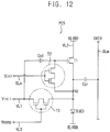
- At least one of the second and third transistors may have a dual gate structure.
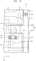
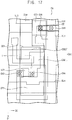
- a first insulating interlayer may be disposed on the control electrode of the first transistor and a first electrode of the first capacitor, the first voltage line and the second electrode of the first capacitor which are disposed on the first insulating interlayer
- a second insulating interlayer may be disposed on the first voltage line and the second electrode of the first capacitor, the m-th data line and a first electrode of the second capacitor which are disposed on the second insulating interlayer
- a third insulating interlayer may be disposed on the m-th data line and a first electrode of the second capacitor, the second voltage line and a second electrode of the second capacitor which are disposed on the third insulating interlayer.
- a method of a display apparatus which includes a plurality of pixels which respectively comprises an organic light emitting diode.
- the method includes applying a low voltage of a first driving signal to an anode electrode of the organic light emitting diode to initialize the anode electrode, applying a low voltage of a first power source signal to a first electrode of a first transistor to diode-connect the first transistor, dividing a data voltage applied to a data line using first and second capacitors which are connected in series to apply divided voltage to a control electrode of the first transistor; and applying a high voltage of the first driving signal to the control electrode of the first transistor to emit a light from the organic light emitting diode.
- the low voltage of the first power source signal may be lower than the low voltage of the first driving signal, and the low voltages of the first power source signal and the first driving signal may be lower than a voltage of second power source signal applied to a cathode electrode of the organic light emitting diode.
- the low voltage of the first power source signal may be higher than the low voltage of the first driving signal, and the low voltages of the first power source signal and the first driving signal may be lower than a voltage of second power source signal applied to a cathode electrode of the organic light emitting diode.
- a difference between the high and low voltages of the first driving signal may be applied to a control electrode of the first transistor, a high voltage of the first driving signal being preset based on a turn-on voltage of the first transistor.
- the method may further include applying a reference voltage to a data line before the data line receives a data voltage corresponding to a first horizontal line of a plurality of horizontal lines, and applying the reference voltage to the data line after the data line receives a data voltage corresponding to a last horizontal line of a plurality of horizontal lines.
- the data line may receive the reference voltage before a control electrode of the first transistor receives the high voltage of the first driving signal.
- each of initializing the anode electrode, diode-coupling the first transistor and emitting the light from the organic light emitting diode may be simultaneously performed in all pixels.
- a display device includes a plurality of pixels.
- a pixel of the plurality of pixels includes a first transistor comprising a control electrode connected to a first node, a first electrode connected to a second voltage line receiving a first power source signal and a second electrode connected to a second node, a first capacitor connected between a first voltage line receiving a first driving signal and the first node, an organic light emitting diode comprising an anode electrode connected to the second node and a cathode electrode receiving a second power source signal, and a second capacitor connected between an m-th data line and the second node (wherein, 'm' is a natural number.
- the pixel may further include a second transistor comprising a control electrode connected to an n-th scan line (wherein, 'n' is a natural number), a first electrode connected to the first node and a second electrode connected to the second node
- the pixel may further include a third transistor comprising a control electrode connected to a third voltage line receiving a second driving signal, a first electrode connected to the first voltage line and a second electrode connected to the second node.
- each of the first, second and third transistors may be an N-type transistor, and a low voltage of the first driving signal is greater than a sum of a low voltage of the first power source and a threshold voltage of the first transistor and less than a sum of the second power source signal and a turn on voltage of the organic light emitting diode.
- each of the first, second and third transistors is a P-type transistor, and a low voltage of the first power source signal is greater than a low voltage of the first driving signal and less than the second power source signal.
- the pixel circuit may include only three transistors and two capacitors and thus, an ultra high definition display may be easily designed using the pixel circuit.
- the compensating period in the frame period may be freely controlled and thus, sufficiently obtained.
- whether the organic light emitting diode emits or not the light may be controlled by adjusting a level of the first power source signal.
- FIG. 1 is a block diagram illustrating a display apparatus according to an embodiment of the invention.
- the display apparatus may include a controller 100, a display part 110, a data driver 130, a scan driver 150 and a voltage generator 170.
- the controller 100 may be configured to generally control the display apparatus to display an image on the display part 110.
- the controller 100 is configured to receive a control signal 101c and image data 101d.
- the controller 100 is configured to provide the data driver 130 with a data control signal 103c and the image data 103d in order to drive the data driver 130.
- the controller 100 is configured to provide the scan driver 150 with a scan control signal 105c in order to drive the scan driver 150.
- the controller 100 is configured to provide the voltage generator 170 with a voltage control signal 107c in order to drive the voltage generator 170.
- the controller 100 is configured to drive the display part 110 during a frame period which may include an initializing period, a compensating period, a data-programming period and a light-emitting period.
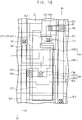
- the display part 110 may include a plurality of pixels P, a plurality of data lines DL1,.., DLm,..., DLM, a plurality of scan lines SL1,..., SLn,..., SLN, a first voltage line VL1, a second voltage line VL2 and a third voltage line VL3.
- Each of the plurality of pixels P may include an organic light emitting diode and three transistors and two capacitors, which drive the organic light emitting diode.
- the data lines DL1, ..., DLm, ..., DLM may respectively extend in a first direction D1 and be arranged in a second direction D2 crossing the first direction D1.
- Each data line DLm is configured to transfer a data voltage to pixels P in a same pixel-column which are arranged in the first direction D1.
- the scan lines SL1,..., SLn,..., SLN may extend in the second direction D2 and be arranged in the first direction D1.
- Each scan line SLn is configured to transfer a scan signal to pixels P in a same pixel-row which are arranged in the second direction D2.
- the first voltage line VL1 may transfer a first driving signal Vinit to the plurality of pixels P and the plurality of pixels P may commonly use the first voltage line VL1.
- the second voltage line VL2 may transfer a first power source signal ELVDD to the plurality of pixels P and the plurality of pixels P may commonly use the second voltage line VL2.
- the third voltage line VL3 may transfer a second driving signal Vcomp to the plurality of pixels P and the plurality of pixels P may commonly use the third voltage line VL3.
- the data driver 130 is configured to provide the data lines DL1,.., DLm,..., DLM with the data voltage corresponding to the image data during the data-programming period of the frame period.
- the data driver 130 is configured to provide the data lines DL1,.., DLm,..., DLM with a reference voltage before or after the data-programming period.
- the reference voltage may be equal to or lower than a black voltage corresponding to a black grayscale.
- the scan driver 150 is configured to sequentially provide the scan lines SL1,..., SLn,..., SLN with the scan signals.
- the scan signal may have a high voltage and a low voltage.
- the voltage generator 170 is configured to generate the first driving signal Vinit, the second driving signal Vcomp, the first power source signal ELVDD and a second power source signal ELVSS.
- the first driving signal Vinit is applied to the first voltage line VL1 and has a high voltage and a low voltage.
- the high voltage and the low voltage of the first driving signal Vinit may have predetermined high and low voltages for driving the pixel P, respectively.
- the second driving signal Vcomp is applied to the third voltage line VL3 and has a high voltage and a low voltage.
- the high voltage and the low voltage of the second driving signal Vcomp may respectively correspond to the high voltage and the low voltage of the scan signal.
- the first power source signal ELVDD is applied to the second voltage line VL2 and has a high voltage and a low voltage.
- the high voltage of the first power source signal ELVDD may have a high voltage of a normal positive power source signal and the low voltage of the first power source signal ELVDD may have a predetermined low voltage for driving the pixel P.
- the second power source signal ELVSS is applied to a common electrode of the pixels P, that is a cathode electrode of an organic light emitting diode and may have a low voltage of a normal negative power source signal.
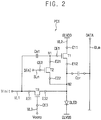
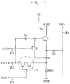
- FIG. 2 is a circuit diagram illustrating a pixel circuit according to an embodiment of the invention.
- the pixel circuit PC1 may be included in the pixel P of the display part 110.
- the pixel circuit PC1 is an equivalent circuit of the pixel P.
- the pixel circuit PC1 may include a first transistor T1, a second transistor T2, a third transistor T3, a first capacitor Cst, a second capacitor Cpr and an organic light emitting diode OLED.
- each of the first, second and third transistors T1, T2 and T3 may be an N-type transistor.
- the N-type transistor may be turned on when a high voltage is applied to a control electrode, and turned off when a low voltage is applied to the control electrode.
- the high voltage may be a turn-on voltage of the N-type transistor and the low voltage may be a turn-off voltage of the N-type transistor.
- the first transistor T1 may include a control electrode CE1 connected to a first node N1, a first electrode E11 connected to a second voltage line VL2 and a second electrode E12 connected to a second node N2.
- the second voltage line VL2 is configured to receive the first power source signal ELVDD.
- the first power source signal ELVDD may have a high voltage which is a voltage of a normal positive power source signal and a low voltage which is a predetermined low voltage for driving the pixel circuit PC1.
- the first power source signal ELVDD may have the low voltage during the compensating period in which a threshold voltage of the first transistor T1 is compensated, and the high voltage during a remaining period of the frame period except for the compensating period.
- the second transistor T2 may include a control electrode CE2 connected to the n-th scan line SLn, a first electrode E21 connected to the first node N1 and a second electrode E22 connected to the second node N2.
- the n-th scan line SLn is configured to receive an n-th scan signal S(n).
- the n-th scan signal S(n) may have a high voltage which turns on the second transistor T2 and a low voltage which turns off the second transistor T2.
- the second transistor T2 may diode-couple the first transistor T1 during the compensating period. That is, the second transistor T2 may connect the control electrode CE1 and the second node N2 of the first transistor T1 during the compensating period.
- the third transistor T3 may include a control electrode CE3 connected to the third voltage line VL3, a first electrode E31 connected to the first voltage line VL1 and a second electrode E32 connected to the second node N2.
- the first voltage line VL1 is configured to receive a first driving signal Vinit.
- the first driving signal Vinit may have high and low voltages which are predetermined high and low voltages driving the pixel circuit PC1.
- the first driving signal Vinit has the high voltage during the light-emitting period during which the organic light emitting diode OLED emits the light, and the low voltage during a remaining period of the frame period except for the light-emitting period.
- the third voltage line VL3 is configured to receive the second driving signal Vcomp.
- the second driving signal Vcomp may have a high voltage which turns on the third transistor T3 and a low voltage which turns off the third transistor T3.
- the first capacitor Cst may be connected between the first voltage line VL1 and the first node N1.
- the first capacitor Cst may store a node voltage applied to the first node N1.
- the second capacitor Cpr may be connected between the second node N2 and m-th data line DLm.
- the second capacitor Cpr may store the data voltage applied to the m-th data line DLm.
- the first and second capacitors Cst and Cpr may be serially connected between the m-th data line DLm and the first voltage line VL1 through the second transistor T2.
- the data voltage applied to the m-th data line DLm may be divided by a voltage division ratio of the first and second capacitors Cst and Cpr and divided data voltage may be applied to the first node N1.
- the organic light emitting diode OLED may include an anode electrode connected to the second node N2 and a cathode electrode which receives the second power source signal ELVSS.
- a driving current corresponding to the data voltage applied to the first node N1 may flow through the organic light emitting diode OLED and thus, the organic light emitting diode OLED may emit the light.
- FIG. 3 is a timing chart illustrating a plurality of input signals of a display apparatus according to an embodiment of the invention.
- the display part may receive a plurality of input signals.
- the plurality of input signal may include the first power source signal ELVDD applied to the second voltage line VL2, the first driving signal Vinit applied to the first voltage line VL1, the second driving signal Vcomp applied to the third voltage line VL3, a plurality of scan signals S(1),.., S(n),.. S(N) applied to the plurality of scan lines, a data voltage DATA applied to the plurality of data lines and the second power source signal ELVSS applied to the cathode electrode of the organic light emitting diode OLED.
- the data voltage DATA may be referred to as a data voltage applied to the m-th data line DLm of the plurality of data lines.
- the frame period may include a first period 'a' during which the anode electrode of the organic light emitting diode OLED is initialized, a second period 'b' during which the threshold voltage of the first transistor T1 is compensated, a third period 'c' during which the data voltage is applied to the pixel and a fourth period 'd' during which the organic light emitting diode OLED emit the light.
- the first voltage line VL1 receives a low voltage initL of the first driving signal Vinit.
- the low voltage initL of the first driving signal Vinit may be defined as the following Equation 1. ELVDD L + V th , T 1 ⁇ Init L ⁇ ELVSS + V on , OLED
- Equation 1 Vth, T1 represents a threshold voltage of the first transistor T1
- Von OLED represents a minimum voltage of the organic light emitting diode OLED while the organic light emitting diode OLED emits the light ('a turn on voltage of the organic light emitting diode OLED').
- the third voltage line VL3 may receive a high voltage VGH of the second driving signal Vcomp.
- the high voltage VGH of the second driving signal Vcomp may have a turn-on voltage of the third transistor T3.
- the high voltage VGH of the second driving signal Vcomp may be about 10 V.
- the second voltage line VL2 may receive a high voltage ELVDDH of the first power source signal ELVDD.
- the high voltage ELVDDH of the first power source signal ELVDD may have a voltage of a normal positive power source signal.
- the low voltage initL of the first driving signal Vinit may be about -2.2 V
- the high voltage ELVDD H of the first power source signal ELVDD may be about 7 V
- the low voltage ELVDDL of the first power source signal ELVDD may be about -7 V
- the second power source signal ELVSS may be about 0 V.
- the plurality of scan lines SL1,.., SLn,..., SLN may simultaneously receive the high voltages VGH of the plurality of scan signals S(1),.., S(n),.. S(N).
- the high voltage VGH of the scan signal may have a turn-on voltage of the second transistor T2.
- the high voltage VGH of the scan signal may be about 10 V.
- the plurality of data lines DL1,.., DLm,..., DLM may receive a reference voltage Vref.
- the reference voltage Vref may be equal to or lower than a lowest voltage in a voltage range of the data voltage. For example, when the voltage range of the data voltage is about 0.5V to about 7.5 V, the reference voltage Vref may be equal to or lower than about 0.5 V.
- the anode electrodes of the organic light emitting diodes OLED which is connected to the second node N2 and the first node N1 in all pixels may be initialized by the low voltage initL of the first driving signal Vinit, simultaneously.
- the first voltage line VL1 is configured to receive the low voltage initL of the first driving signal Vinit.
- the third voltage line VL3 is configured to receive a low voltage VGL of second driving signal Vcomp.
- the low voltage VGL of the second driving signal Vcomp may have a turn-off voltage of the third transistor T3.
- the low voltage VGL of the second driving signal Vcomp may be about -10 V.
- the second voltage line VL2 is configured to receive a low voltage ELVDDL of the first power source signal ELVDD.
- the low voltage ELVDDL of the first power source signal ELVDD may be about -7 V.
- the plurality of scan lines SL1,.., SLn,..., SLN is configured to simultaneously receive high voltages VGH of the plurality of scan signals S(1),.., S(n),.. S(N) as the first period 'a'.
- the plurality of data lines DL1,.., DLm,..., DLM is configured to receive the reference voltage Vref as the first period 'a'.
- the threshold voltages of the first transistors T1 in all pixels may be simultaneously compensated using the sum voltage of the low voltage ELVDDL of the first power source signal ELVDD and the threshold voltage Vth, T1 of corresponding first transistor T1.
- the second voltage line VL2 is configured to receive a high voltage ELVDDH of the first power source signal ELVDD.
- the first voltage line VL1 is configured to receive the low voltage initL of the first driving signal Vinit.
- the third voltage line VL3 is configured to receive the low voltage VGL of the second driving signal Vcomp.
- the plurality of scan lines SL1,.., SLn,.., SLN is configured to sequentially receive high voltages VGH of the plurality of scan signals S(1),.., S(n),.. S(N).
- the plurality of data lines DL1,.., DLm,..., DLM is configured to receive the data voltage DATA respectively corresponding to the plurality of horizontal lines in synchronization with the high voltages VGH of the plurality of scan signals S(1),.., S(n),.. S(N).
- the first node N1 is configured to receive divided data voltage by a voltage division ratio of the first and second capacitors Cst and Cpr during a corresponding horizontal period of the pixel.
- the third period 'c' may include at least one holding period during which the plurality of data lines DL1,.., DLm,..., DLM is configured to receive a reference voltage Vref.
- the holding period may be disposed before a first horizontal period in which a data voltage of a first horizontal line is applied to the plurality of data lines DL1,.., DLm,..., DLM and after a last horizontal period in which a data voltage of a last horizontal line is applied to the plurality of data lines DL1,.., DLm,..., DLM. Therefore, the plurality of data lines DL1,.., DLm,..., DLM may be maintained into the reference voltage Vref during the holding period.
- the second voltage line VL2 is configured to receive the high voltage ELVDDH of the first power source signal ELVDD.
- the first voltage line VL1 is configured to receive a high voltage initH of the first driving signal Vinit.
- the high voltage initH of the first driving signal Vinit may be determined based on a turn-on voltage of the first transistor T1.
- the high voltage initH of the first driving signal Vinit may be about 6.5 V.
- the third voltage line VL3 is configured to receive the low voltage VGL of the second driving signal Vcomp.
- the plurality of scan lines SL1,.., SLn,..., SLN is configured to simultaneously receive the low voltages VGL of the plurality of scan signals S(1),.., S(n),.. S(N).
- the plurality of data lines DL1,.., DLm,..., DLM is configured to simultaneously receive the reference voltage Vref.
- driving current corresponding to the data voltage applied to the first node N1 may be provided to the organic light emitting diode OLED and the organic light emitting diode OLED may emit the light.
- the organic light emitting diodes OLED in all pixels may simultaneously emit the light.
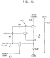
- FIGS. 4A and 4B are conceptual diagrams illustrating a method of driving the pixel circuit according to an embodiment of the invention.
- the first period 'a' may correspond to an initializing period of the organic light emitting diode OLED.
- the low voltage initL of first driving signal Vinit is applied to the first voltage line VL1
- the high voltage VGH of the second driving signal Vcomp is applied to the third voltage line VL3
- the high voltage ELVDDH of the first power source signal ELVDD is applied to the second voltage line VL2.
- the n-th scan line SLn receives the high voltage VGH of the n-th scan signal S(n).
- the m-th data line DLm receives the reference voltage Vref.
- the low voltage initL of the first driving signal Vinit is applied to the first node N1.
- the second transistor T2 is turned on in response to the high voltage VGH of the n-th scan signal S(n).
- the third transistor T3 is turned on in response to the high voltage VGH of the second driving signal Vcomp, and then the low voltage initL of the first driving signal Vinit is provided to the second node N2.
- the anode electrode of the organic light emitting diode OLED connected to the second node N2 may be initialized by the low voltage initL of the first driving signal Vinit.
- the organic light emitting diode OLED may be initialized.
- FIGS. 5A and 5B are conceptual diagrams illustrating a method of driving the pixel circuit according to an embodiment of the invention.
- the second period 'b' may correspond to a compensating period during which the threshold voltage of the first transistor T1 is compensated.
- the low voltage initL of the first driving signal Vinit is applied to the first voltage line VL1
- the low voltage VGL of the second driving signal Vcomp is applied to the third voltage line VL3
- the low voltage ELVDDL of the first power source signal ELVDD is applied to the second voltage line VL2.
- the n-th scan line SLn receives the high voltage VGH of the n-th scan signal S(n).
- the m-th data line receives the reference voltage Vref.
- the second transistor T2 is turned on in response to the high voltage VGH of the n-th scan signal S(n).
- the third transistor T3 is turned off in response to the low voltage VGL of the second driving signal Vcomp.
- the control electrode CE1 and the second electrode E12 of the first transistor T1 are connected to each other and the low voltage ELVDD L of the first power source signal ELVDD is applied to the first electrode E11 of the first transistor T1.
- the transistor is diode-connected.
- a voltage applied to the first electrode E11 of the first transistor T1 is determined to be lower than the low voltage initL of the first driving signal Vinit applied to the second electrode E12 and thus, the first electrode E11 may drive as the source and the second electrode E12 may drive as the drain.
- the gate and drain of the first transistor T1 are connected to each other and the first transistor T1 is diode-connected.
- the first node N1 connected to the control electrode CE1 of the first transistor T1 receives a voltage corresponding to a sum voltage of the low voltage ELVDD L of the first power source signal and the threshold voltage Vth,T1 of the first transistor T1.
- the threshold voltage of the first transistor T1 may be compensated.
- a length of the second period 'b' may be freely adjusted in the frame period and thus a sufficient compensating period may be obtained.
- FIGS. 6A and 6B are conceptual diagrams illustrating a method of driving the pixel circuit according to an embodiment of the invention.
- the third period 'c' may correspond to a data-programming period during which the data voltage is applied to the plurality of pixels.
- the low voltage initL of the first driving signal Vinit is applied to the first voltage line VL1
- the low voltage VGL of the second driving signal Vcomp is applied to the third voltage line VL3
- the high voltage ELVDD H of the first power source signal ELVDD is applied to the second voltage line VL2.
- the n-th scan line SLn receives a high voltage VGH of an n-th scan signal S(n) during an n-th horizontal period Hn of the third period 'c'.
- the m-th data line DLm receives an n-th data voltage Vdata(n) of an n-th horizontal line corresponding to the n-th horizontal period Hn during the n-th horizontal period Hn.
- the first transistor T1 which has the control electrode CE1 connected to the first node N1 is turned off because V GS of the first transistor T1 is less than the threshold voltage Vth,T1.
- the first node N1 receives a voltage (ELVDD L + Vth,T1+ ⁇ Vdata) corresponding to a sum voltage of the low voltage ELVDD L of the first power source signal ELVDD, the threshold voltage Vth,T1 of the first transistor T1 and a divided voltage ⁇ Vdata.
- the third transistor T3 is turned off in response to the low voltage VGL of the second driving signal Vcomp.
- the second transistor T2 is turned on in response to the high voltage VGH of the n-th scan signal S(n), and then the first node N1 is connected to the second node N2.
- the first capacitor Cst and the second capacitor Cpr are connected to the first node N1 in series by the turned-on second transistor T2.
- the n-th data voltage Vdata(n) corresponding to the pixel circuit PC1 is applied to the m-th data line DLm.
- the m-th data line DLm receives a difference voltage ⁇ Vdata between the n-th data voltage Vdata(n) and the reference voltage Vref.
- the first and second capacitors Cst and Cpr which are connected to the first node N1 in series has a voltage division ratio ⁇ corresponding to the first node N1.
- the voltage division ratio ⁇ and the difference voltage ⁇ Vdata may be defined as the following Equation 2.
- the difference voltage ⁇ Vdata is divided by the voltage division ratio ⁇ of the first and second capacitors Cst and Cpr and divided voltage ⁇ Vdata corresponding to the n-th data voltage Vdata(n) is applied to the first node N1.
- a voltage defined as the following Equation 3 may be applied to the first node N1 during the n-th horizontal period Hn.
- the third period 'c' may include a first holding period h1 corresponding to an early period of the third period 'c' and a second holding period h2 corresponding to a late period of the third period 'c'.
- the first holding period h1 may correspond to a period which is before a first horizontal period in which a data voltage Vdata(1) of a first horizontal line is applied to the plurality of data lines DL1,.., DLm,..., DLM.
- the reference voltage Vref is applied to the plurality of data lines DL1,.., DLm,..., DLM and thus, the plurality of data lines DL1,.., DLm,..., DLM may hold the reference voltage Vref before the first horizontal period.
- the second holding period h2 may correspond to a period which is after an N-th horizontal period in which the data voltage Vdata(N) of an N-th horizontal line, that is a last horizontal line, is applied to the plurality of data lines DL1,.., DLm,..., DLM.
- the reference voltage Vref is applied to the plurality of data lines DL1,.., DLm,..., DLM and thus, the plurality of data lines DL1,.., DLm,..., DLM may hold the reference voltage Vref after the N-th horizontal period.
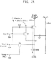
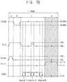
- FIGS. 7A and 7B are conceptual diagrams illustrating a method of driving the pixel circuit according to an embodiment of the invention.
- the fourth period 'd' may correspond to a light-emitting period during which the organic light emitting diode OLED emits the light.
- the high voltage initH of the first driving signal Vinit is applied to the first voltage line VL1
- the low voltage VGL of the second driving signal Vcomp is applied to the third voltage line VL3
- the high voltage ELVDD H of the first power source signal ELVDD is applied to the second voltage line VL2.
- the n-th scan line SLn receives the low voltage VGL of the n-th scan signal S(n).
- the m-th data line DLm receives the reference voltage Vref.
- the high voltage initH of the first driving signal Vinit is applied to the first node N1 and thus, a voltage defined as the following Equation 4 may be applied to the first node N1.
- a difference voltage ⁇ Vinit represents a difference voltage between the high and low voltages initH and initL of the first driving signal Vinit.
- the first transistor T1 When the voltage defined as the following Equation 4 is applied to the control electrode CE1 of the first transistor T1, the first transistor T1 is turned on based on the difference voltage ⁇ Vinit.
- the second transistor T2 is turned off in response to the low voltage VGL of the n-th scan signal S(n) and the third transistor T3 is turned off in response to the low voltage VGL of the second driving signal Vcomp.
- the first transistor T1 is turned on and thus, a driving current ID corresponding to the data voltage may flow through the organic light emitting diode OLED.
- the organic light emitting diode OLED may emit the light.
- the pixel circuit may include only three transistors and two capacitors and thus, an ultra high definition display may be easily designed using the pixel circuit.
- the length of the compensating period in the frame period may be freely controlled and thus, a sufficient compensation period is obtained.
- whether the organic light emitting diode emits or not the light may be controlled by adjusting a level of the first power source signal ELVDD.
- FIG. 8 is a circuit diagram illustrating a pixel circuit according to an embodiment of the invention.
- the pixel circuit PC2 may include a first transistor T1, a second transistor T2, a third transistor T3, a first capacitor Cst, a second capacitor Cpr and an organic light emitting diode OLED.
- the pixel circuit PC2 may include three transistors and two capacitors as the pixel circuit PC1 described in the previous embodiment.
- each of the first, second and third transistors T1, T2 and T3 according to the embodiment may be a P-type transistor.
- the P-type transistor is turned on when a control electrode of the P-type transistor receives a low voltage and is turned off when the control electrode of the P-type transistor receives a high voltage.
- the low voltage may be a turn-on voltage of the transistor and the high voltage may be a turn-off voltage of the transistor.
- the first transistor T1 may include a control electrode CE1 connected to a first node N1, a first electrode E11 connected to a second voltage line VL2 and a second electrode E12 connected to a second node N2.
- the second voltage line VL2 is configured to receive the first power source signal ELVDD.
- the first power source signal ELVDD may have a high voltage which is a voltage of a normal positive power source signal and a low voltage which is a predetermined low voltage for driving the pixel circuit PC2.
- the second transistor T2 may include a control electrode CE2 connected to the n-th scan line SLn, a first electrode E21 connected to the first node N1 and a second electrode E22 connected to the second node N2.
- the n-th scan line SLn is configured to receive an n-th scan signal S(n).
- the n-th scan signal S(n) may have a low voltage which turns on the second transistor T2 and a high voltage which turns off the second transistor T2.
- the third transistor T3 may include a control electrode CE3 connected to the third voltage line VL3, a first electrode E31 connected to the first voltage line VL1 and a second electrode E32 connected to the second node N2.
- the first voltage line VL1 is configured to receive a first driving signal Vinit and the third voltage line VL3 is configured to receive a second driving signal Vcomp.
- the first driving signal Vinit may have high and low voltages which are predetermined high and low voltages for driving the pixel circuit PC2.
- the second driving signal Vcomp may have a low voltage which turns on the third transistor T3 and a high voltage which turns off the third transistor T3.
- the high and low voltages of the second driving signal Vcomp may be equal to those of the n-th scan signal S(n), respectively.
- the first capacitor Cst may be connected between the first voltage line VL1 and the first node N1.
- the first capacitor Cst may store a node voltage applied to the first node N1.
- the second capacitor Cpr may be connected between the second node N2 and m-th data line DLm.
- the second capacitor Cpr may store the data voltage applied to the m-th data line DLm.
- the first and second capacitors Cst and Cpr may be connected to the first node in series N1 through the second transistor T2.
- the data voltage applied to the m-th data line DLm may be divided by a voltage division ratio of the first and second capacitors Cst and Cpr and then, divided data voltage may be applied to the first node N1.
- the organic light emitting diode OLED may include an anode electrode connected to the second node N2 and a cathode electrode which receives the second power source signal ELVSS.
- the second power source signal ELVSS may have a low voltage of a normal negative power source signal.
- a driving current corresponding to the data voltage of the first node N1 may flow through the organic light emitting diode OLED and thus, the organic light emitting diode OLED may emit the light.
- FIG. 9 is a timing chart illustrating a plurality of input signals of a display apparatus according to an embodiment of the invention.
- the frame period may include a first period 'a' during which the anode electrode of the organic light emitting diode OLED is initialized, a second period 'b' during which the threshold voltage of the first transistor T1 is compensated, a third period 'c' during which the data voltage is programmed and a fourth period 'd' during which the organic light emitting diode OLED emit the light.
- a first voltage line VL1 receives a low voltage initL of the first driving signal Vinit.
- the third voltage line VL3 may receive a low voltage VGL of the second driving signal Vcomp.
- the second voltage line VL2 may receive a low voltage ELVDD L of the first power source signal ELVDD.
- the cathode electrode of the organic light emitting diode OLED may receive a second power source signal ELVSS.
- the low voltage initL of the first driving signal Vinit and the second power source signal ELVSS may be defined as the following Equation 5.
- the low voltage initL of the first driving signal Vinit may be about -6 V
- the low voltage ELVDDL of the first power source signal ELVDD may be about -2 V
- the second power source signal ELVSS may be about 0 V.
- the plurality of scan lines SL1,.., SLn,..., SLN may simultaneously receive the low voltages VGL of the plurality of scan signals S(1),.., S(n),.. S(N).
- an n-th scan line SLn receives the low voltage VGL of an n-th scan signal S(n).
- the low voltage VGL of the scan signal may be about -10 V.
- the plurality of data lines DL1,.., DLm,..., DLM may receive a reference voltage Vref.
- the reference voltage Vref may be equal to or lower than a lowest voltage in a voltage range of the data voltage. For example, when the voltage range of the data voltage is about 1.5 V to about 4.5 V, the reference voltage Vref may be equal to or lower than about 1.5 V.
- the low voltage initL of the first driving signal Vinit is applied to the first node N1.
- the first transistor T1 is turned on in response to the low voltage initL of the first driving signal Vinit applied to the first node N1.
- the second transistor T2 is turned on in response to the low voltage VGL of the n-th scan signal S(n).
- the anode electrode of the organic light emitting diode OLED connected to the second node N2 may be initialized by the low voltage initL of the first driving signal Vinit.
- the low voltage ELVDD L of the first power source signal ELVDD may be higher than the low voltage initL of the first driving signal Vinit.
- the low voltage ELVDDL of the first power source signal ELVDD is applied to the second node N2 through the turned-on first transistor T1.
- the anode electrodes of the organic light emitting diodes OLED in all pixels may be initialized by the low voltage initL of the first driving signal Vinit, simultaneously.
- the first voltage line VL1 is configured to receive the low voltage initL of the first driving signal Vinit
- the third voltage line VL3 is configured to receive the high voltage VGH of second driving signal Vcomp
- the second voltage line VL2 is configured to receive a low voltage ELVDD L of the first power source signal ELVDD.
- the cathode electrode of the organic light emitting diode OLED is configured to receive the second power source signal ELVSS.
- the plurality of scan lines SL1,.., SLn,..., SLN is configured to simultaneously receive low voltages VGL of the plurality of scan signals S(1),.., S(n),.. S(N) as the first period 'a'.
- the plurality of data lines DL1,.., DLm,..., DLM is configured to receive the reference voltage Vref as the first period 'a'.
- the second transistor T2 is turned on in response to the low voltage VGL of the n-th scan signal S(n).
- the third transistor T3 is turned off in response to the high voltage VGH of the second driving signal Vcomp.
- the control electrode CE1 and the second electrode E12 of the first transistor T1 are connected to each other through the turned-on second transistor T2.
- the first transistor T1 of the P-type transistor includes the first electrode E11 receiving the low voltage EVDDL of the first power source signal ELVDD and the second electrode E12 receiving the low voltage initL of the first driving signal.
- the first electrode E11 of the first transistor T1 may drive as the source and the second electrode E12 may drive as the drain. Therefore, the gate and the drain of the first transistor T1 may be connected through the turned-on second transistor T2 and thus, the first transistor T1 may be diode-connected.
- the first node N1 connected to the control electrode CE1 of the first transistor T1 receives a voltage corresponding to a difference voltage between the low voltage ELVDD L of the first power source signal and the threshold voltage Vth,T1 of the first transistor T1.
- the threshold voltage of the first transistor T1 may be a negative voltage.
- the threshold voltage of the first transistor T1 being the P-type transistor may be an absolute value of the threshold voltage being the negative number.
- the threshold voltages of the first transistors T1 in all pixels may be simultaneously compensated using the difference voltage between the low voltage ELVDDL of the first power source signal ELVDD and the threshold voltage Vth,T1 of corresponding first transistor T1.
- the first voltage line VL1 is configured to receive the low voltage initL of the first driving signal Vinit
- the third voltage line VL3 is configured to receive the high voltage VGH of the second driving signal Vcomp
- the second voltage line VL2 is configured to receive the low voltage ELVDDL of the first power source signal ELVDD.
- the cathode electrode of the organic light emitting diode OLED is configured to receive the second power source signal ELVSS.
- the plurality of scan lines SL1,.., SLn,.., SLN is configured to sequentially receive low voltages VGL of the plurality of scan signals S(1),.., S(n),.. S(N).
- the plurality of data lines DL1,.., DLm,..., DLM is configured to receive the data voltage DATA corresponding to the plurality of horizontal lines in synchronization with the low voltages VGL of the plurality of scan signals S(1),.., S(n),.. S(N).
- the n-th scan line SLn receives the low voltage VGL of an n-th scan signal S(n) during an n-th horizontal period Hn of the third period 'c'.
- the m-th data line DLm receives an n-th data voltage Vdata(n) of an n-th horizontal line corresponding to the n-th horizontal period Hn during the n-th horizontal period Hn.
- the low voltage ELVDD L of the first power source signal ELVDD is applied to the first electrode E11 of the first transistor T1
- a voltage corresponding to the n-th data voltage Vdata(n) is applied to the second electrode E12 of the first transistor T1.
- a high voltage higher than a voltage of the first electrode E11 of the first transistor T1 is applied to the second electrode E12 of the first transistor T1 and thus, a current may not flow through the first transistor T1.
- the second transistor T2 is turned on in response to the low voltage VGL of the n-th scan signal S(n), and then the first node N1 is connected to the second node N2.
- the first capacitor Cst and the second capacitor Cpr are connected to the first node N1 in series through the turned-on second transistor T2.
- the first transistor T1 which has the control electrode CE1 connected to the first node N1 is turned off.
- the first node N1 receives a voltage corresponding to a difference voltage between the low voltage ELVDD L of the first power source signal ELVDD and the threshold voltage Vth,T1 of the first transistor T1.
- the third transistor T3 is turned off in response to the high voltage VGH of the second driving signal Vcomp.
- the n-th data voltage Vdata(n) corresponding to the pixel circuit PC2 is applied to the m-th data line DLm.
- the first and second capacitors Cst and Cpr which are connected to the first node N1 in series has a voltage division ratio ⁇ corresponding to the first node N1.
- the difference voltage ⁇ Vdata is divided by the voltage division ratio ⁇ of the first and second capacitors Cst and Cpr and the divided voltage ⁇ ⁇ Vdata corresponding to the n-th data voltage Vdata(n) is applied to the first node N1.
- a voltage defined as the following Equation 6 may be applied to the first node N1 during the n-th horizontal period Hn.
- the third period 'c' may include a first holding period h1 corresponding to an early period of the third period 'c' and a second holding period h2 corresponding to a late period of the third period 'c'.
- the first holding period h1 may correspond to a period which is before a first horizontal period in which the data voltage Vdata(1) of a first horizontal line is applied to the plurality of data lines DL1,.., DLm,..., DLM.
- the reference voltage Vref is applied to the plurality of data lines DL1,.., DLm,..., DLM and thus, the plurality of data lines DL1,.., DLm,..., DLM may hold the reference voltage Vref before the first horizontal period.
- the second holding period h2 may correspond to a period which is after an N-th horizontal period in which the data voltage Vdata(N) of an N-th horizontal line, that is a last horizontal line, is applied to the plurality of data lines DL1,.., DLm,..., DLM.
- the reference voltage Vref is applied to the plurality of data lines DL1,.., DLm,..., DLM and thus, the plurality of data lines DL1,.., DLm,..., DLM may hold the reference voltage Vref after the N-th horizontal period.
- the high voltage initH of the first driving signal Vinit is applied to the first voltage line VL1.
- the high voltage initH of the first driving signal Vinit may be determined to a predetermined voltage for turning on the first transistor T1.
- the high voltage initH of the first driving signal Vinit may be about 2.5 V.
- the third voltage line VL3 is configured to receive the high voltage VGH of the second driving signal Vcomp.
- the second voltage line VL2 is configured to receive the high voltage ELVDDH of the first power source signal ELVDD.
- the high voltage ELVDDH of the first power source signal ELVDD may be about 7 V.
- the cathode electrode of the organic light emitting diode OLED is configured to receive the second power source signal ELVSS.
- the plurality of scan lines SL1,.., SLn" SLN is configured to simultaneously receive high voltages VGH of the plurality of scan signals S(1),.., S(n),.. S(N).
- the plurality of data lines DL1,.., DLm, ..., DLM is configured to simultaneously receive the reference voltage Vref.
- the first node N1 may have a node voltage as the following Equation 7.
- Equation 7 ELVDD L ⁇ V th , T 1 + ⁇ ⁇ ⁇ V data + ⁇ V init
- the difference voltage ⁇ Vinit represents a difference voltage between the high and low voltages initH and initL of the first driving signal Vinit.
- the first transistor T1 When the node voltage defined as the following Equation 7 is applied to the control electrode CE1 of the first transistor T1, the first transistor T1 is turned on based on the difference voltage ⁇ Vinit. Then, the high voltage ELVDD H of the first power source signal ELVDD is applied to the first electrode E11 of the first transistor T1 and thus, a driving current corresponding to the data voltage applied to the first node N, may flow through the organic light emitting diode OLED.
- the second transistor T2 is turned off in response to the high voltage VGH of the n-th scan signal S(n) and the third transistor T3 is turned off in response to the high voltage VGH of the second driving signal Vcomp.
- driving currents corresponding to data voltages applied to the plurality of pixels may flow through organic light emitting diodes OLEDs in the plurality of pixels and thus, the organic light emitting diodes OLEDs in the plurality of pixels may simultaneously emit the light.
- the pixel circuit may include only three transistors and two capacitors and thus, an ultra high definition display may be easily designed using the pixel circuit.
- the compensating period in the frame period may be freely controlled and thus, sufficiently obtained.
- whether the organic light emitting diode emits or not the light may be controlled by adjusting a level of the first power source signal.
- FIGS. 10 to 12 are circuit diagrams illustrating pixel circuits according to embodiments of the invention.
- a pixel circuit PC3 may include a first transistor T1, a second transistor T2, a third transistor T3, a first capacitor Cst, a second capacitor Cpr and an organic light emitting diode OLED.
- the second transistor T2 may have a dual gate structure to avoid a leakage current.
- Each of the first, second and third transistors T1, T2 and T3 in the pixel circuit PC3 may be a N-type transistor.
- the pixel circuit PC3 having the N-type transistor may drive as the pixel circuit PC1 described in the previous embodiment referring to FIGS. 2 and 3 .
- each of the first, second and third transistors T1, T2 and T3 in the pixel circuit PC3 may be an P-type transistor.
- the pixel circuit PC3 having the P-type transistor may drive as the pixel circuit PC2 described in the previous embodiment referring to FIGS. 8 and 9 .
- a pixel circuit PC4 may include a first transistor T1, a second transistor T2, a third transistor T3, a first capacitor Cst, a second capacitor Cpr and an organic light emitting diode OLED.
- the third transistor T3 may have a dual gate structure to avoid a leakage current.
- Each of the first, second and third transistors T1, T2 and T3 in the pixel circuit PC4 may be a N-type transistor.
- the pixel circuit PC4 having the N-type transistor may drive as the pixel circuit PC1 described in the previous embodiment referring to FIGS. 2 and 3 .
- each of the first, second and third transistors T1, T2 and T3 in the pixel circuit PC4 may be an P-type transistor.
- the pixel circuit PC4 having the P-type transistor may drive as the pixel circuit PC2 described in the previous embodiment referring to FIGS. 8 and 9 .
- a pixel circuit PC5 may include a first transistor T1, a second transistor T2, a third transistor T3, a first capacitor Cst, a second capacitor Cpr and an organic light emitting diode OLED.
- the second and third transistors T2 and T3 may have a dual gate structure to avoid a leakage current.
- Each of the first, second and third transistors T1, T2 and T3 in the pixel circuit PC5 may be a N-type transistor.
- the pixel circuit PC5 having the N-type transistor may drive as the pixel circuit PC1 described in the previous embodiment referring to FIGS. 2 and 3 .
- each of the first, second and third transistors T1, T2 and T3 in the pixel circuit PC5 may be an P-type transistor.
- the pixel circuit PC5 having the P-type transistor may drive as the pixel circuit PC2 described in the previous embodiment referring to FIGS. 8 and 9 .
- the pixel circuit includes only three transistors and two capacitors and thus, an ultra high definition display may be easily designed using the pixel circuit.
- the length of the compensating period in the frame period may be freely controlled and thus, a sufficient compensating period is obtained.
- whether the organic light emitting diode emits or not the light may be controlled by adjusting a level of the first power source signal.
- the leakage current of the transistor may be avoided.
- FIG. 13 is a plan view illustrating a display part of a display apparatus according to an embodiment of the invention.
- the pixel circuit may be formed in a pixel circuit area PA.
- the first voltage line VL1, the second voltage line VL2, the third voltage line VL3, the n-th scan line SLn, the m-th data line DLm, first transistor T1, the second transistor T2, the third transistor T3, the first capacitor Cst and the second capacitor Cpr may be formed in the pixel circuit area PA.
- the first voltage line VL1 may transfer a first driving signal Vinit and extend in the first direction D1.
- the second voltage line VL2 may transfer a first power source signal ELVDD and extend in the first direction D1.
- the third voltage line VL3 may transfer a second driving signal Vcomp and extend in the second direction D2.
- the n-th scan line SLn may transfer an n-th scan signal S(n) and extend in the second direction D2.
- the m-th data line DLm may transfer a data voltage and extend in the first direction D1.
- the m-th data line DLm may be formed across a central area of the pixel circuit area PA.
- the first transistor T1 may include a control electrode CE1, a first electrode E11, and a second electrode E12.
- the control electrode CE1 may have an island shape and be formed in the central area of the pixel circuit area PA.
- the first electrode E11 may be defined in a portion area of the second voltage line VL2 which is connected to an active pattern ACT through a first contact part CH1.
- the second electrode E12 may be defined in a portion area of the second capacitor Cpr which is connected to the active pattern ACT through a second contact part CH2.
- the second transistor T2 may include a control electrode CE2, a first electrode E21, and a second electrode E22.
- the control electrode CE2 may be defined in a portion area of the n-th scan line SLn.
- the first electrode E21 may be defined as an electrode which is connected to the active pattern ACT through a third contact part CH3.
- the second electrode E22 may be defined in a portion area of the second capacitor Cpr which is connected to the active pattern ACT through the second contact part CH2.
- the first electrode E21 may be connected to the control electrode CE1 of the first transistor T1 through a fourth contact part CH4.
- the third transistor T3 may include a control electrode CE3, a first electrode E31, and a second electrode E32.
- the control electrode CE3 may be defined in a portion area of the third voltage line VL2.
- the first electrode E31 may be defined in a portion area of the third voltage line VL3 which is connected to the active pattern ACT through a fifth contact part CH5.
- the second electrode E32 may be defined in a portion area of the second capacitor Cpr which is connected to the active pattern ACT through the second contact part CH2.
- the third voltage line VL3 may be connected to the third voltage line VL3 which is formed in an adjacent pixel circuit area, through a connection line and a sixth contact part CH6.
- the first capacitor Cst may be defined in an overlapping area in which an electrode extending in the second direction D2 from the first voltage line VL1 overlaps with the control electrode CE1 of the first transistor T1.
- the second capacitor Cpr may be defined in an overlapping area in which an electrode having the island shape in the central area of the pixel circuit area PA overlaps with the m-th data line DLm.
- the second capacitor Cpr may overlap with the first capacitor Cst.
- FIG. 14 is a cross-sectional view taken along a line I-I' of FIG. 13 .
- FIGS. 15 to 19 are plan views illustrating a method of manufacturing of the display part according to an embodiment of the invention.
- the display part may include a base substrate 111.
- the base substrate 111 may include an insulation material.
- the base substrate 111 may include a glass, a transparent plastic, a transparent metal oxide, etc.
- the active pattern ACT may be disposed on the base substrate 111.
- the active pattern ACT may include silicon.
- the active pattern ACT may be formed of a semiconductor oxide including a binary compound (ABx), a ternary compound (ABxCy), a quaternary compound (ABxCyDz), etc. which contain indium, zinc, gallium, tin, titanium, aluminum, hafnium (Hf), zirconium (Zr), magnesium (Mg), etc. These compounds may be used alone or in combination thereof.
- the active pattern ACT may include first to sixth areas a1, a2, a3, a4, a5 and a6.
- the first to sixth areas a1, a2, a3, a4, a5 and a6 may be doped with an impurity, and thus may have electrical conductivity higher than those of other regions of the active pattern ACT.
- the first to sixth areas a1, a2, a3, a4, a5 and a6 may be first and second electrodes of first, second and third transistors T1, T2 and T3.
- first to sixth areas a1, a2, a3, a4, a5 and a6 may not be clearly defined and first to sixth areas a1, a2, a3, a4, a5 and a6 may be electrically connected to each other.
- a gate insulating layer 112 may be disposed on the active pattern ACT.
- the gate insulating layer 112 may include a silicon compound, metal oxide, etc.
- the gate insulation layer may include silicon oxide, silicon nitride, silicon oxynitride, aluminum oxide, tantalum oxide, hafnium oxide, zirconium oxide, titanium oxide, etc., which may be used alone or in combination thereof.
- the gate insulation layer 112 may have a multilayer structure including a silicon oxide layer and silicon nitride layer.
- a first conductive pattern MET1 which is patterned from a first conductive layer, may be disposed on the gate insulating layer 112.
- the first conductive layer may include metal, alloy, metal nitride, conductive metal oxide, transparent conductive material, etc., which may be used alone or in combination thereof.
- the first conductive pattern MET1 may include the n-th scan line SLn, the control electrode CE2 of the second transistor T2, the third voltage line VL3, the control electrode CE3 of the third transistor T3, the control electrode CE1 of the first transistor T1, and the first capacitor electrode CSE1 of the first capacitor Cst.
- the n-th scan line SLn may extend in the second direction D2.
- the control electrode CE2 of the second transistor T2 may be defined in a portion area of the n-th scan line SLn.
- the third voltage line VL3 may be disposed in parallel with the n-th scan line SLn.
- the control electrode CE3 of the third transistor T3 may be defined in a portion area of the third voltage line VL3.
- the control electrode CE1 of the first transistor T1 may have an island shape and be disposed in a central area of the pixel circuit area PA.
- the first capacitor electrode CSE1 of the first capacitor Cst may be defined in a portion area of the control electrode CE1.
- a first insulating interlayer 113 may be disposed on the first conductive pattern MET1.
- the first insulating interlayer 113 may be formed of a silicon oxide, a silicon nitride, a silicon oxynitride, and etc. These may be used alone or in combination with each other.
- the pixel circuit area PA may include a third contact part CH3, a fourth contact part CH4 and a fifth contact part CH5.
- the gate insulating layer 112 and the first insulating interlayer 113 are etched to form the third and fifth contact parts CH3 and CH5.
- the insulating interlayer 113 are etched to form the fourth contact part CH4.
- a second conductive pattern MET2 which is patterned from a second conductive layer, may be disposed on the first insulating interlayer 113.
- the second conductive layer metal, alloy, metal nitride, conductive metal oxide, transparent conductive material, etc., which may be used alone or in combination thereof.
- the second conductive pattern MET2 may include the first voltage line VL1, a second capacitor electrode CSE2 of the first capacitor Cst, a first electrode E21 of the second transistor T2 and the first electrode E31 of the third transistor T3.
- the first voltage line VL1 may extend in the first direction D1.
- the second capacitor electrode CSE2 of the first capacitor Cst may extend in the second direction D2 from the first voltage line VL1.
- the first capacitor Cst may be defined by the first electrode CSE1 of the first conductive pattern MET1 and the second capacitor electrode CSE2 of the second conductive pattern MET2.
- a first end portion of the first electrode E21 may be connected to the active pattern ACT through the third contact part CH3 and a second end portion of the first electrode E21 may be connected to the control electrode CE1 of the first transistor T1 through the fourth contact part CH4.
- the first electrode E31 of the third transistor T3 may be defined in a portion area of the first voltage line VL1 and be connected to the active pattern ACT through the fifth contact part CH5.
- a second insulating interlayer 114 may be disposed on the second conductive pattern MET2.
- the pixel circuit area PA may include a sixth contact part CH6 in which the first and second insulating interlayers 113 and 114 are etched.
- a third conductive pattern MET3 which is patterned from a third conductive layer, may be disposed on the second insulating interlayer 114.
- the third conductive pattern MET3 may include the m-th data line DLm, a third capacitor electrode CPE1 of the second capacitor Cpr and a connection electrode EE.
- the m-th data line DLm may extend in the first direction D1 and be disposed in the central area of the pixel circuit area PA.
- the third capacitor electrode CPE1 of the second capacitor Cpr may extend from the m-th data line DLm.
- connection electrode EE may be connected to the third voltage line VL3 and a third voltage line VL3 which is disposed in an adjacent pixel circuit area, through the sixth contact part CH6.
- a third insulating interlayer 115 may be disposed on the third conductive pattern MET3.
- the pixel circuit area PA may include a first contact part CH1 and a second contact part CH2 in which the gate insulating layer 112, the first insulating interlayer 113, the second insulating interlayer 114 and the third insulating interlayer 115 are etched.
- a fourth conductive pattern MET4 which is patterned from a fourth conductive layer may be disposed on the third insulating interlayer 115.
- the fourth conductive pattern MET4 may include the second voltage line VL2, the first electrode E11 of the first transistor T1, a fourth capacitor electrode CPE2 of the second capacitor Cpr, the second electrode E12 of the first transistor T1, the second electrode E22 of the second transistor T2 and the second electrode E32 of the third transistor T3.
- the second voltage line VL2 may extend in the first direction D1 and may define a width of the pixel circuit area PA in the first direction D1 together with a second voltage line VL2 in the adjacent pixel circuit area PA.
- the first electrode E11 of the first transistor T1 may be defined in a portion area of the second voltage line VL2 connected to the active pattern AC through the first contact part CH1.
- the fourth capacitor electrode CPE2 of the second capacitor Cpr may have an island shape and be disposed in the central area of the pixel circuit area PA.
- the second capacitor Cpr may be defined by the third capacitor electrode CPE1 of the third conductive pattern MET3 and the fourth capacitor electrode CPE2 of the fourth conductive pattern MET4.
- the second electrode E12 of the first transistor T1, the second electrode E22 of the second transistor T2 and the second electrode E32 of the third transistor T3 may respectively defined in portion areas of the fourth capacitor electrode CPE2 connected to the active pattern ACT through the second contact part CH2.
- a fourth insulating interlayer 116 may be disposed on the fourth conductive pattern MET4.
- the fourth insulating interlayer 116 may be formed with a high thickness to sufficiently cover the fourth conductive pattern MET4.
- the pixel circuit area PA may include a seventh contact part CH7 in which the fourth insulating interlayer 116 is etched.
- a first pixel electrode PE1 may be disposed on the fourth insulating interlayer 116.
- the first pixel electrode PE1 may correspond to the anode electrode of the organic light emitting diode.
- a pixel defining layer 117 may be disposed on the fourth insulating interlayer 116 on which the first pixel electrode PE1 is formed.
- the pixel defining layer 117 may form an opening on a portion area of the first pixel electrode PE1, and the organic light emitting layer EL may be disposed in the opening. Thus, the organic light emitting layer EL may be on the first pixel electrode PE1 exposed through the opening of the pixel defined layer 117.
- a second pixel electrode PE2 may be disposed on the organic light emitting layer EL.
- the second pixel electrode PE2 may correspond to the cathode electrode of the organic light emitting diode.
- the second pixel electrode PE2 may be commonly disposed in the plurality of pixel circuit areas.
- the pixel circuit may include only three transistors and two capacitors and thus, an ultra high definition display may be easily designed using the pixel circuit.
- the length of the compensating period in the frame period may be freely controlled and thus, a sufficient compensating period is obtained.
- whether the organic light emitting diode emits or not the light may be controlled by adjusting a level of the first power source signal.
Landscapes
- Engineering & Computer Science (AREA)
- Physics & Mathematics (AREA)
- Computer Hardware Design (AREA)
- General Physics & Mathematics (AREA)
- Theoretical Computer Science (AREA)
- Control Of El Displays (AREA)
- Control Of Indicators Other Than Cathode Ray Tubes (AREA)
- Electroluminescent Light Sources (AREA)
Abstract
Description
- Embodiments of the inventive concept relate to a display apparatus and a method of driving the display apparatus. More particularly, example embodiments of the inventive concept relate to a display apparatus having a simple pixel structure and a method of driving the display apparatus.
- Recently, various flat panel display devices that reduce weight and volume have been developed. The flat panel display devices include a liquid crystal display (LCD) device, a field emission display (FED) device, a plasma display panel (PDP) device, an organic light emitting display (OLED) device, etc.
- The OLED device has advantages such as rapid response speed and low power consumption because the OLED device among the flat panel display devices displays an image using an organic light emitting diode that emits a light during recombination of electrons and holes.
- Embodiments of the inventive concept set out to provide a display apparatus having improved display quality in a standby mode that is a low-power mode.
- Embodiments of the inventive concept also seek to provide a method of driving such a display apparatus.
- According to an embodiment of the inventive concept, there is provided a display apparatus. The display apparatus includes a plurality of pixels. A pixel of the plurality of pixels includes a first capacitor connected between a first voltage line receiving a first driving signal and a first node, a first transistor comprising a control electrode connected to the first node, a first electrode connected to a second voltage line receiving a first power source signal and a second electrode connected to a second node, an organic light emitting diode comprising an anode electrode connected to the second node and a cathode electrode receiving a second power source signal, a second capacitor connected between an m-th data line and the second node (wherein, 'm' is a natural number) and a second transistor comprising a control electrode connected to an n-th scan line (wherein, 'n' is a natural number), a first electrode connected to the first node and a second electrode connected to the second node.
- In an embodiment of the invention, the pixel may further include a third transistor comprising a control electrode connected to a third voltage line receiving a second driving signal, a first electrode connected to the first voltage line and a second electrode connected to the second node.
- In an embodiment of the invention, each of the first, second and third transistors may be an N-type transistor.
- In an embodiment of the invention, during a first period of a frame period, the first voltage line may receive a low voltage of a first driving signal, the second voltage line may receive a high voltage of the first power source signal, the third voltage line may receive a high voltage of the second driving signal and the n-th scan line may receive a high voltage of a scan signal.
- In an embodiment of the invention, during a second period of the frame period, the first voltage line may receive a low voltage of the first driving signal, the second voltage line may receive a low voltage of the first power source signal lower than the low voltage of the first driving signal, the third voltage line may receive a low voltage of the second driving signal, and the n-th scan line may receive a high voltage of the scan signal.
- In an embodiment of the invention, during a third period of the frame period, the first voltage line may receive a low voltage of the first driving signal, the second voltage line may receive a high voltage of the first power source signal, the third voltage line may receive a low voltage of the second driving signal, the n-th scan line may receive a high voltage of the scan signal during an n-th horizontal period in the third period, and the m-th data line may receive a data voltage corresponding to a plurality of horizontal lines.
- In an embodiment of the invention, during the n-th horizontal period, a data voltage corresponding to an n-th horizontal line may be divided by a voltage division ratio of the first and second capacitors which are connected in series and divided voltage may be applied to the first node.
- In an embodiment of the invention, the m-th data line may receive s a reference voltage before the m-th data line receives a data voltage corresponding to a first horizontal line of a plurality of horizontal lines, and the m-th data line may receive a reference voltage after the m-th data line receives a data voltage corresponding to a last horizontal line of a plurality of horizontal lines.
- In an embodiment of the invention, the m-th data line may receive a reference voltage before the first voltage line receives a high voltage of the first driving signal and, the reference voltage may be equal to or lower than a lowest voltage in a voltage range of the data voltage.
- In an embodiment of the invention, during a fourth period of the frame period, the first voltage line may receive a high voltage of the first driving signal, the second voltage line may receive a high voltage of the first power source signal, the third voltage line may receive a low voltage of the second driving signal, and the n-th scan line may receive a low voltage of the scan signal.
- In an embodiment of the invention, when a difference voltage between the high voltage and the low voltage of the first driving signal is applied to the first node, the first transistor may be turned on and a driving current corresponding to the data voltage applied to the first node may flow through the organic light emitting diode.
- In an embodiment of the invention, each of the first, second and third transistors may be a P-type transistor.
- In an embodiment of the invention, during a first period, the first voltage line may receive a low voltage of the first driving signal, the second voltage line may receive a low voltage of the first power source signal, the third voltage line may receive a low voltage of the second driving signal, and the n-th scan line receives a low voltage of the scan signal.
- In an embodiment of the invention, the low voltage of the first power source signal may be higher than the low voltage of the first driving signal.
- In an embodiment of the invention, during a second period of the frame period, the first voltage line may receive a low voltage of the first driving signal, the second voltage line may receive a low voltage of the first power source signal, the third voltage line may receive a high voltage of the second driving signal and the n-th scan line may receive a low voltage of the scan signal.
- In an embodiment of the invention, during a third period of the fame period, the first voltage line may receive a low voltage of the first driving signal, the second voltage line may receive a low voltage of the first power source signal, the third voltage line may receive a high voltage of the second driving signal, the n-th scan line may receive a low voltage of the scan signal during an n-th horizontal period in the third period, and the m-th data line may receive a data voltage corresponding to a plurality of horizontal lines.
- In an embodiment of the invention, during the n-th horizontal period, a data voltage corresponding to an n-th horizontal line may be divided by a voltage division ratio of the first and second capacitors which are connected in series and divided voltage may be applied to the first node.
- In an embodiment of the invention, the m-th data line may receive a reference voltage before the m-th data line receives a data voltage corresponding to a first horizontal line of a plurality of horizontal lines, and the m-th data line may receive a reference voltage after the m-th data line receives a data voltage corresponding to a last horizontal line of a plurality of horizontal lines.
- In an embodiment of the invention, the m-th data line may receive a reference voltage before the first voltage line receives a high voltage of the first driving signal, and the reference voltage mat be equal to or lower than a lowest voltage in a voltage range of the data voltage.
- In an embodiment of the invention, during a fourth period of the frame period, the first voltage line may receive a high voltage of the first driving signal, the second voltage line may receive a high voltage of the first power source signal, the third voltage line may receive a high voltage of the second driving signal, and the n-th scan line may receive a high voltage of the scan signal.
- In an embodiment of the invention, when a difference voltage between the high voltage and the low voltage of the first driving signal may be applied to the first node, the first transistor is turned on and a driving current corresponding to the data voltage applied to the first node may flow through the organic light emitting diode.
- In an embodiment of the invention, at least one of the second and third transistors may have a dual gate structure.
- In an embodiment of the invention, a first insulating interlayer may be disposed on the control electrode of the first transistor and a first electrode of the first capacitor, the first voltage line and the second electrode of the first capacitor which are disposed on the first insulating interlayer, a second insulating interlayer may be disposed on the first voltage line and the second electrode of the first capacitor, the m-th data line and a first electrode of the second capacitor which are disposed on the second insulating interlayer, and a third insulating interlayer may be disposed on the m-th data line and a first electrode of the second capacitor, the second voltage line and a second electrode of the second capacitor which are disposed on the third insulating interlayer.
- According to an embodiment of the inventive concept, there is provided a method of a display apparatus which includes a plurality of pixels which respectively comprises an organic light emitting diode. The method includes applying a low voltage of a first driving signal to an anode electrode of the organic light emitting diode to initialize the anode electrode, applying a low voltage of a first power source signal to a first electrode of a first transistor to diode-connect the first transistor, dividing a data voltage applied to a data line using first and second capacitors which are connected in series to apply divided voltage to a control electrode of the first transistor; and applying a high voltage of the first driving signal to the control electrode of the first transistor to emit a light from the organic light emitting diode.
- In an embodiment of the invention, when the first transistor may be an N-type transistor, the low voltage of the first power source signal may be lower than the low voltage of the first driving signal, and the low voltages of the first power source signal and the first driving signal may be lower than a voltage of second power source signal applied to a cathode electrode of the organic light emitting diode.
- In an embodiment of the invention, when the first transistor may be a P-type transistor, the low voltage of the first power source signal may be higher than the low voltage of the first driving signal, and the low voltages of the first power source signal and the first driving signal may be lower than a voltage of second power source signal applied to a cathode electrode of the organic light emitting diode.
- In an embodiment of the invention, a difference between the high and low voltages of the first driving signal may be applied to a control electrode of the first transistor, a high voltage of the first driving signal being preset based on a turn-on voltage of the first transistor.
- In an embodiment of the invention, the method may further include applying a reference voltage to a data line before the data line receives a data voltage corresponding to a first horizontal line of a plurality of horizontal lines, and applying the reference voltage to the data line after the data line receives a data voltage corresponding to a last horizontal line of a plurality of horizontal lines.
- In an embodiment of the invention, the data line may receive the reference voltage before a control electrode of the first transistor receives the high voltage of the first driving signal.
- In an embodiment of the invention, each of initializing the anode electrode, diode-coupling the first transistor and emitting the light from the organic light emitting diode may be simultaneously performed in all pixels.
- According to an embodiment of the inventive concept, there is provided a display device. The display device includes a plurality of pixels. A pixel of the plurality of pixels includes a first transistor comprising a control electrode connected to a first node, a first electrode connected to a second voltage line receiving a first power source signal and a second electrode connected to a second node, a first capacitor connected between a first voltage line receiving a first driving signal and the first node, an organic light emitting diode comprising an anode electrode connected to the second node and a cathode electrode receiving a second power source signal, and a second capacitor connected between an m-th data line and the second node (wherein, 'm' is a natural number.
- In an embodiment of the invention, the pixel may further include a second transistor comprising a control electrode connected to an n-th scan line (wherein, 'n' is a natural number), a first electrode connected to the first node and a second electrode connected to the second node
- In an embodiment of the invention, the pixel may further include a third transistor comprising a control electrode connected to a third voltage line receiving a second driving signal, a first electrode connected to the first voltage line and a second electrode connected to the second node.
- In an embodiment of the invention, each of the first, second and third transistors may be an N-type transistor, and a low voltage of the first driving signal is greater than a sum of a low voltage of the first power source and a threshold voltage of the first transistor and less than a sum of the second power source signal and a turn on voltage of the organic light emitting diode.
- In an embodiment of the invention, each of the first, second and third transistors is a P-type transistor, and a low voltage of the first power source signal is greater than a low voltage of the first driving signal and less than the second power source signal.
- According to the inventive concept, the pixel circuit may include only three transistors and two capacitors and thus, an ultra high definition display may be easily designed using the pixel circuit. In addition, the compensating period in the frame period may be freely controlled and thus, sufficiently obtained. In addition, whether the organic light emitting diode emits or not the light may be controlled by adjusting a level of the first power source signal.
- At least some of the above and other features of the invention are set out in the claims.
- The above and other features and advantages of the inventive concept will be made more apparent by describing in detail embodiments thereof with reference to the accompanying drawings, in which:
-
FIG. 1 is a block diagram illustrating a display apparatus according to an embodiment of the invention; -
FIG. 2 is a circuit diagram illustrating a pixel circuit according to an embodiment of the invention; -
FIG. 3 is a timing chart illustrating a plurality of input signals of a display apparatus according to an embodiment of the invention; -
FIGS. 4A and4B are conceptual diagrams illustrating a method of driving the pixel circuit according to an embodiment of the invention; -
FIGS. 5A and5B are conceptual diagrams illustrating a method of driving the pixel circuit according to an embodiment of the invention; -
FIGS. 6A and6B are conceptual diagrams illustrating a method of driving the pixel circuit according to an embodiment of the invention; -
FIGS. 7A and7B are conceptual diagrams illustrating a method of driving the pixel circuit according to an embodiment of the invention; -
FIG. 8 is a circuit diagram illustrating a pixel circuit according to an embodiment of the invention; -
FIG. 9 is a timing chart illustrating a plurality of input signals of a display apparatus according to an embodiment of the invention; -
FIGS. 10 to 12 are circuit diagrams illustrating pixel circuits according to embodiments of the invention; -
FIG. 13 is a plan view illustrating a display part of a display apparatus according to an embodiment of the invention; -
FIG. 14 is a cross-sectional view taken along a line I-I' ofFIG. 13 ; and -
FIGS. 15 to 19 are plan views illustrating a method of manufacturing of the display part according to an embodiment of the invention. - Hereinafter, embodiments of the inventive concept will be explained in detail with reference to the accompanying drawings.
-
FIG. 1 is a block diagram illustrating a display apparatus according to an embodiment of the invention. - Referring to
FIG. 1 , the display apparatus may include acontroller 100, adisplay part 110, adata driver 130, ascan driver 150 and avoltage generator 170. - The
controller 100 may be configured to generally control the display apparatus to display an image on thedisplay part 110. Thecontroller 100 is configured to receive acontrol signal 101c andimage data 101d. Thecontroller 100 is configured to provide thedata driver 130 with adata control signal 103c and theimage data 103d in order to drive thedata driver 130. Thecontroller 100 is configured to provide thescan driver 150 with ascan control signal 105c in order to drive thescan driver 150. Thecontroller 100 is configured to provide thevoltage generator 170 with avoltage control signal 107c in order to drive thevoltage generator 170. - The
controller 100 is configured to drive thedisplay part 110 during a frame period which may include an initializing period, a compensating period, a data-programming period and a light-emitting period. - The
display part 110 may include a plurality of pixels P, a plurality of data lines DL1,.., DLm,..., DLM, a plurality of scan lines SL1,..., SLn,..., SLN, a first voltage line VL1, a second voltage line VL2 and a third voltage line VL3. - Each of the plurality of pixels P may include an organic light emitting diode and three transistors and two capacitors, which drive the organic light emitting diode.
- The data lines DL1, ..., DLm, ..., DLM may respectively extend in a first direction D1 and be arranged in a second direction D2 crossing the first direction D1. Each data line DLm is configured to transfer a data voltage to pixels P in a same pixel-column which are arranged in the first direction D1.
- The scan lines SL1,..., SLn,..., SLN may extend in the second direction D2 and be arranged in the first direction D1. Each scan line SLn is configured to transfer a scan signal to pixels P in a same pixel-row which are arranged in the second direction D2.
- The first voltage line VL1 may transfer a first driving signal Vinit to the plurality of pixels P and the plurality of pixels P may commonly use the first voltage line VL1.
- The second voltage line VL2 may transfer a first power source signal ELVDD to the plurality of pixels P and the plurality of pixels P may commonly use the second voltage line VL2.
- The third voltage line VL3 may transfer a second driving signal Vcomp to the plurality of pixels P and the plurality of pixels P may commonly use the third voltage line VL3.
- The
data driver 130 is configured to provide the data lines DL1,.., DLm,..., DLM with the data voltage corresponding to the image data during the data-programming period of the frame period. - In addition, the
data driver 130 is configured to provide the data lines DL1,.., DLm,..., DLM with a reference voltage before or after the data-programming period. The reference voltage may be equal to or lower than a black voltage corresponding to a black grayscale. - The
scan driver 150 is configured to sequentially provide the scan lines SL1,..., SLn,..., SLN with the scan signals. The scan signal may have a high voltage and a low voltage. - The
voltage generator 170 is configured to generate the first driving signal Vinit, the second driving signal Vcomp, the first power source signal ELVDD and a second power source signal ELVSS. - The first driving signal Vinit is applied to the first voltage line VL1 and has a high voltage and a low voltage. The high voltage and the low voltage of the first driving signal Vinit may have predetermined high and low voltages for driving the pixel P, respectively.
- The second driving signal Vcomp is applied to the third voltage line VL3 and has a high voltage and a low voltage. The high voltage and the low voltage of the second driving signal Vcomp may respectively correspond to the high voltage and the low voltage of the scan signal.
- The first power source signal ELVDD is applied to the second voltage line VL2 and has a high voltage and a low voltage. The high voltage of the first power source signal ELVDD may have a high voltage of a normal positive power source signal and the low voltage of the first power source signal ELVDD may have a predetermined low voltage for driving the pixel P.
- The second power source signal ELVSS is applied to a common electrode of the pixels P, that is a cathode electrode of an organic light emitting diode and may have a low voltage of a normal negative power source signal.
-
FIG. 2 is a circuit diagram illustrating a pixel circuit according to an embodiment of the invention. - Referring to
FIGS. 1 and2 , the pixel circuit PC1 may be included in the pixel P of thedisplay part 110. The pixel circuit PC1 is an equivalent circuit of the pixel P. - The pixel circuit PC1 may include a first transistor T1, a second transistor T2, a third transistor T3, a first capacitor Cst, a second capacitor Cpr and an organic light emitting diode OLED.
- According to this embodiment, each of the first, second and third transistors T1, T2 and T3 may be an N-type transistor. The N-type transistor may be turned on when a high voltage is applied to a control electrode, and turned off when a low voltage is applied to the control electrode. According to the embodiment, the high voltage may be a turn-on voltage of the N-type transistor and the low voltage may be a turn-off voltage of the N-type transistor.
- The first transistor T1 may include a control electrode CE1 connected to a first node N1, a first electrode E11 connected to a second voltage line VL2 and a second electrode E12 connected to a second node N2. The second voltage line VL2 is configured to receive the first power source signal ELVDD.
- The first power source signal ELVDD may have a high voltage which is a voltage of a normal positive power source signal and a low voltage which is a predetermined low voltage for driving the pixel circuit PC1. The first power source signal ELVDD may have the low voltage during the compensating period in which a threshold voltage of the first transistor T1 is compensated, and the high voltage during a remaining period of the frame period except for the compensating period.
- The second transistor T2 may include a control electrode CE2 connected to the n-th scan line SLn, a first electrode E21 connected to the first node N1 and a second electrode E22 connected to the second node N2. The n-th scan line SLn is configured to receive an n-th scan signal S(n). The n-th scan signal S(n) may have a high voltage which turns on the second transistor T2 and a low voltage which turns off the second transistor T2. The second transistor T2 may diode-couple the first transistor T1 during the compensating period. That is, the second transistor T2 may connect the control electrode CE1 and the second node N2 of the first transistor T1 during the compensating period.
- The third transistor T3 may include a control electrode CE3 connected to the third voltage line VL3, a first electrode E31 connected to the first voltage line VL1 and a second electrode E32 connected to the second node N2. The first voltage line VL1 is configured to receive a first driving signal Vinit.
- The first driving signal Vinit may have high and low voltages which are predetermined high and low voltages driving the pixel circuit PC1. The first driving signal Vinit has the high voltage during the light-emitting period during which the organic light emitting diode OLED emits the light, and the low voltage during a remaining period of the frame period except for the light-emitting period.
- The third voltage line VL3 is configured to receive the second driving signal Vcomp. The second driving signal Vcomp may have a high voltage which turns on the third transistor T3 and a low voltage which turns off the third transistor T3.
- The first capacitor Cst may be connected between the first voltage line VL1 and the first node N1. The first capacitor Cst may store a node voltage applied to the first node N1.
- The second capacitor Cpr may be connected between the second node N2 and m-th data line DLm. The second capacitor Cpr may store the data voltage applied to the m-th data line DLm.
- The first and second capacitors Cst and Cpr may be serially connected between the m-th data line DLm and the first voltage line VL1 through the second transistor T2. The data voltage applied to the m-th data line DLm may be divided by a voltage division ratio of the first and second capacitors Cst and Cpr and divided data voltage may be applied to the first node N1.
- The organic light emitting diode OLED may include an anode electrode connected to the second node N2 and a cathode electrode which receives the second power source signal ELVSS.
- When the transistor T1 is turned on, a driving current corresponding to the data voltage applied to the first node N1 may flow through the organic light emitting diode OLED and thus, the organic light emitting diode OLED may emit the light.
-
FIG. 3 is a timing chart illustrating a plurality of input signals of a display apparatus according to an embodiment of the invention. - Referring to
FIGS. 1 ,2 and3 , the display part may receive a plurality of input signals. The plurality of input signal may include the first power source signal ELVDD applied to the second voltage line VL2, the first driving signal Vinit applied to the first voltage line VL1, the second driving signal Vcomp applied to the third voltage line VL3, a plurality of scan signals S(1),.., S(n),.. S(N) applied to the plurality of scan lines, a data voltage DATA applied to the plurality of data lines and the second power source signal ELVSS applied to the cathode electrode of the organic light emitting diode OLED. The data voltage DATA may be referred to as a data voltage applied to the m-th data line DLm of the plurality of data lines. - The frame period may include a first period 'a' during which the anode electrode of the organic light emitting diode OLED is initialized, a second period 'b' during which the threshold voltage of the first transistor T1 is compensated, a third period 'c' during which the data voltage is applied to the pixel and a fourth period 'd' during which the organic light emitting diode OLED emit the light.
- Referring to the first period 'a', the first voltage line VL1 receives a low voltage initL of the first driving signal Vinit. The low voltage initL of the first driving signal Vinit may be defined as the following
Equation 1.
- In
Equation 1, Vth,T1 represents a threshold voltage of the first transistor T1, Von,OLED represents a minimum voltage of the organic light emitting diode OLED while the organic light emitting diode OLED emits the light ('a turn on voltage of the organic light emitting diode OLED'). - The third voltage line VL3 may receive a high voltage VGH of the second driving signal Vcomp. The high voltage VGH of the second driving signal Vcomp may have a turn-on voltage of the third transistor T3. For example, the high voltage VGH of the second driving signal Vcomp may be about 10 V.
- The second voltage line VL2 may receive a high voltage ELVDDH of the first power source signal ELVDD. The high voltage ELVDDH of the first power source signal ELVDD may have a voltage of a normal positive power source signal.
- For example, the low voltage initL of the first driving signal Vinit may be about -2.2 V, the high voltage ELVDDH of the first power source signal ELVDD may be about 7 V, the low voltage ELVDDL of the first power source signal ELVDD may be about -7 V, and the second power source signal ELVSS may be about 0 V.
- The plurality of scan lines SL1,.., SLn,..., SLN may simultaneously receive the high voltages VGH of the plurality of scan signals S(1),.., S(n),.. S(N). The high voltage VGH of the scan signal may have a turn-on voltage of the second transistor T2. For example, the high voltage VGH of the scan signal may be about 10 V.
- The plurality of data lines DL1,.., DLm,..., DLM may receive a reference voltage Vref. The reference voltage Vref may be equal to or lower than a lowest voltage in a voltage range of the data voltage. For example, when the voltage range of the data voltage is about 0.5V to about 7.5 V, the reference voltage Vref may be equal to or lower than about 0.5 V.
- During the first period 'a', the anode electrodes of the organic light emitting diodes OLED which is connected to the second node N2 and the first node N1 in all pixels may be initialized by the low voltage initL of the first driving signal Vinit, simultaneously.
- Referring to the second period 'b', the first voltage line VL1 is configured to receive the low voltage initL of the first driving signal Vinit.
- The third voltage line VL3 is configured to receive a low voltage VGL of second driving signal Vcomp. The low voltage VGL of the second driving signal Vcomp may have a turn-off voltage of the third transistor T3. For example, the low voltage VGL of the second driving signal Vcomp may be about -10 V.
- The second voltage line VL2 is configured to receive a low voltage ELVDDL of the first power source signal ELVDD. For example, the low voltage ELVDDL of the first power source signal ELVDD may be about -7 V.
- The plurality of scan lines SL1,.., SLn,..., SLN is configured to simultaneously receive high voltages VGH of the plurality of scan signals S(1),.., S(n),.. S(N) as the first period 'a'.
- The plurality of data lines DL1,.., DLm,..., DLM is configured to receive the reference voltage Vref as the first period 'a'.
- During the second period 'b', the threshold voltages of the first transistors T1 in all pixels may be simultaneously compensated using the sum voltage of the low voltage ELVDDL of the first power source signal ELVDD and the threshold voltage Vth,T1 of corresponding first transistor T1.
- Referring to the third period 'c', the second voltage line VL2 is configured to receive a high voltage ELVDDH of the first power source signal ELVDD.
- The first voltage line VL1 is configured to receive the low voltage initL of the first driving signal Vinit.
- The third voltage line VL3 is configured to receive the low voltage VGL of the second driving signal Vcomp.
- The plurality of scan lines SL1,.., SLn,.., SLN is configured to sequentially receive high voltages VGH of the plurality of scan signals S(1),.., S(n),.. S(N).
- The plurality of data lines DL1,.., DLm,..., DLM is configured to receive the data voltage DATA respectively corresponding to the plurality of horizontal lines in synchronization with the high voltages VGH of the plurality of scan signals S(1),.., S(n),.. S(N).
- The first node N1 is configured to receive divided data voltage by a voltage division ratio of the first and second capacitors Cst and Cpr during a corresponding horizontal period of the pixel.
- In addition, the third period 'c' may include at least one holding period during which the plurality of data lines DL1,.., DLm,..., DLM is configured to receive a reference voltage Vref. The holding period may be disposed before a first horizontal period in which a data voltage of a first horizontal line is applied to the plurality of data lines DL1,.., DLm,..., DLM and after a last horizontal period in which a data voltage of a last horizontal line is applied to the plurality of data lines DL1,.., DLm,..., DLM. Therefore, the plurality of data lines DL1,.., DLm,..., DLM may be maintained into the reference voltage Vref during the holding period.
- Referring to the fourth period 'd', the second voltage line VL2 is configured to receive the high voltage ELVDDH of the first power source signal ELVDD.
- The first voltage line VL1 is configured to receive a high voltage initH of the first driving signal Vinit. The high voltage initH of the first driving signal Vinit may be determined based on a turn-on voltage of the first transistor T1. For example, the high voltage initH of the first driving signal Vinit may be about 6.5 V.
- The third voltage line VL3 is configured to receive the low voltage VGL of the second driving signal Vcomp.
- The plurality of scan lines SL1,.., SLn,..., SLN is configured to simultaneously receive the low voltages VGL of the plurality of scan signals S(1),.., S(n),.. S(N).
- The plurality of data lines DL1,.., DLm,..., DLM is configured to simultaneously receive the reference voltage Vref.
- During the fourth period 'd', driving current corresponding to the data voltage applied to the first node N1 may be provided to the organic light emitting diode OLED and the organic light emitting diode OLED may emit the light. Thus, the organic light emitting diodes OLED in all pixels may simultaneously emit the light.
-
FIGS. 4A and4B are conceptual diagrams illustrating a method of driving the pixel circuit according to an embodiment of the invention. - Referring to
FIGS. 4A and4B , the first period 'a' may correspond to an initializing period of the organic light emitting diode OLED. - In the first period 'a', the low voltage initL of first driving signal Vinit is applied to the first voltage line VL1, the high voltage VGH of the second driving signal Vcomp is applied to the third voltage line VL3, and the high voltage ELVDDH of the first power source signal ELVDD is applied to the second voltage line VL2. The n-th scan line SLn receives the high voltage VGH of the n-th scan signal S(n). The m-th data line DLm receives the reference voltage Vref.
- Referring to a method of driving the pixel circuit PC1, the low voltage initL of the first driving signal Vinit is applied to the first node N1. The second transistor T2 is turned on in response to the high voltage VGH of the n-th scan signal S(n).
- The third transistor T3 is turned on in response to the high voltage VGH of the second driving signal Vcomp, and then the low voltage initL of the first driving signal Vinit is provided to the second node N2. The anode electrode of the organic light emitting diode OLED connected to the second node N2 may be initialized by the low voltage initL of the first driving signal Vinit.
- Therefore, during the first period 'a', the organic light emitting diode OLED may be initialized.
-
FIGS. 5A and5B are conceptual diagrams illustrating a method of driving the pixel circuit according to an embodiment of the invention. - Referring to
FIGS. 5A and5B , the second period 'b' may correspond to a compensating period during which the threshold voltage of the first transistor T1 is compensated. - In the second period 'b', the low voltage initL of the first driving signal Vinit is applied to the first voltage line VL1, the low voltage VGL of the second driving signal Vcomp is applied to the third voltage line VL3, the low voltage ELVDDL of the first power source signal ELVDD is applied to the second voltage line VL2. The n-th scan line SLn receives the high voltage VGH of the n-th scan signal S(n). The m-th data line receives the reference voltage Vref.
- The second transistor T2 is turned on in response to the high voltage VGH of the n-th scan signal S(n). The third transistor T3 is turned off in response to the low voltage VGL of the second driving signal Vcomp.
- When the second transistor T2 is turned on, the control electrode CE1 and the second electrode E12 of the first transistor T1 are connected to each other and the low voltage ELVDDL of the first power source signal ELVDD is applied to the first electrode E11 of the first transistor T1.
- Because a drain electrode E12 which has a higher voltage than a source electrode E11 is connected to the gate, the transistor is diode-connected..
- A voltage applied to the first electrode E11 of the first transistor T1 is determined to be lower than the low voltage initL of the first driving signal Vinit applied to the second electrode E12 and thus, the first electrode E11 may drive as the source and the second electrode E12 may drive as the drain.
- Therefore, when the second transistor T2 is turned on, the gate and drain of the first transistor T1 are connected to each other and the first transistor T1 is diode-connected.
- When the first transistor T1 is diode-connected, the first node N1 connected to the control electrode CE1 of the first transistor T1 receives a voltage corresponding to a sum voltage of the low voltage ELVDDL of the first power source signal and the threshold voltage Vth,T1 of the first transistor T1.
- Therefore, the threshold voltage of the first transistor T1 may be compensated.
- According to the embodiment of the invention, a length of the second period 'b' may be freely adjusted in the frame period and thus a sufficient compensating period may be obtained.
-
FIGS. 6A and6B are conceptual diagrams illustrating a method of driving the pixel circuit according to an embodiment of the invention. - Referring to
FIGS. 6A and6B , the third period 'c' may correspond to a data-programming period during which the data voltage is applied to the plurality of pixels. - In the third period 'c', the low voltage initL of the first driving signal Vinit is applied to the first voltage line VL1, the low voltage VGL of the second driving signal Vcomp is applied to the third voltage line VL3, and the high voltage ELVDDH of the first power source signal ELVDD is applied to the second voltage line VL2. The n-th scan line SLn receives a high voltage VGH of an n-th scan signal S(n) during an n-th horizontal period Hn of the third period 'c'. The m-th data line DLm receives an n-th data voltage Vdata(n) of an n-th horizontal line corresponding to the n-th horizontal period Hn during the n-th horizontal period Hn.
- Referring to the method of driving the pixel circuit PC1, the first transistor T1 which has the control electrode CE1 connected to the first node N1 is turned off because VGS of the first transistor T1 is less than the threshold voltage Vth,T1. The first node N1 receives a voltage (ELVDDL + Vth,T1+αΔVdata) corresponding to a sum voltage of the low voltage ELVDDL of the first power source signal ELVDD, the threshold voltage Vth,T1 of the first transistor T1 and a divided voltage αΔVdata. The third transistor T3 is turned off in response to the low voltage VGL of the second driving signal Vcomp.
- The second transistor T2 is turned on in response to the high voltage VGH of the n-th scan signal S(n), and then the first node N1 is connected to the second node N2. The first capacitor Cst and the second capacitor Cpr are connected to the first node N1 in series by the turned-on second transistor T2.
- The n-th data voltage Vdata(n) corresponding to the pixel circuit PC1 is applied to the m-th data line DLm. The m-th data line DLm receives a difference voltage ΔVdata between the n-th data voltage Vdata(n) and the reference voltage Vref.
- The first and second capacitors Cst and Cpr which are connected to the first node N1 in series has a voltage division ratio α corresponding to the first node N1. The voltage division ratio α and the difference voltage ΔVdata may be defined as the following Equation 2.

- Therefore, the difference voltage ΔVdata is divided by the voltage division ratio α of the first and second capacitors Cst and Cpr and divided voltage αΔVdata corresponding to the n-th data voltage Vdata(n) is applied to the first node N1.
- Therefore, a voltage defined as the following Equation 3 may be applied to the first node N1 during the n-th horizontal period Hn.

- According to the exemplary embodiment, the third period 'c' may include a first holding period h1 corresponding to an early period of the third period 'c' and a second holding period h2 corresponding to a late period of the third period 'c'.
- The first holding period h1 may correspond to a period which is before a first horizontal period in which a data voltage Vdata(1) of a first horizontal line is applied to the plurality of data lines DL1,.., DLm,..., DLM. During the first holding period h1, the reference voltage Vref is applied to the plurality of data lines DL1,.., DLm,..., DLM and thus, the plurality of data lines DL1,.., DLm,..., DLM may hold the reference voltage Vref before the first horizontal period.
- The second holding period h2 may correspond to a period which is after an N-th horizontal period in which the data voltage Vdata(N) of an N-th horizontal line, that is a last horizontal line, is applied to the plurality of data lines DL1,.., DLm,..., DLM. During the second holding period h2, the reference voltage Vref is applied to the plurality of data lines DL1,.., DLm,..., DLM and thus, the plurality of data lines DL1,.., DLm,..., DLM may hold the reference voltage Vref after the N-th horizontal period.
-
FIGS. 7A and7B are conceptual diagrams illustrating a method of driving the pixel circuit according to an embodiment of the invention. - Referring to
FIGS. 7A and7B , the fourth period 'd' may correspond to a light-emitting period during which the organic light emitting diode OLED emits the light. - Referring to the fourth period 'd', the high voltage initH of the first driving signal Vinit is applied to the first voltage line VL1, the low voltage VGL of the second driving signal Vcomp is applied to the third voltage line VL3, and the high voltage ELVDDH of the first power source signal ELVDD is applied to the second voltage line VL2. The n-th scan line SLn receives the low voltage VGL of the n-th scan signal S(n). The m-th data line DLm receives the reference voltage Vref.
- Referring to the method of driving the pixel circuit PC1, the high voltage initH of the first driving signal Vinit is applied to the first node N1 and thus, a voltage defined as the following Equation 4 may be applied to the first node N1.

- In Equation 4, a difference voltage ΔVinit represents a difference voltage between the high and low voltages initH and initL of the first driving signal Vinit.
- When the voltage defined as the following Equation 4 is applied to the control electrode CE1 of the first transistor T1, the first transistor T1 is turned on based on the difference voltage ΔVinit.
- The second transistor T2 is turned off in response to the low voltage VGL of the n-th scan signal S(n) and the third transistor T3 is turned off in response to the low voltage VGL of the second driving signal Vcomp.
- Therefore, the first transistor T1 is turned on and thus, a driving current ID corresponding to the data voltage may flow through the organic light emitting diode OLED. The organic light emitting diode OLED may emit the light.
- According to the embodiment of the invention, the pixel circuit may include only three transistors and two capacitors and thus, an ultra high definition display may be easily designed using the pixel circuit. In addition, the length of the compensating period in the frame period may be freely controlled and thus, a sufficient compensation period is obtained. In addition, whether the organic light emitting diode emits or not the light may be controlled by adjusting a level of the first power source signal ELVDD.
-
FIG. 8 is a circuit diagram illustrating a pixel circuit according to an embodiment of the invention. - Referring to
FIG. 8 , the pixel circuit PC2 may include a first transistor T1, a second transistor T2, a third transistor T3, a first capacitor Cst, a second capacitor Cpr and an organic light emitting diode OLED. - The pixel circuit PC2 may include three transistors and two capacitors as the pixel circuit PC1 described in the previous embodiment. However, each of the first, second and third transistors T1, T2 and T3 according to the embodiment may be a P-type transistor. The P-type transistor is turned on when a control electrode of the P-type transistor receives a low voltage and is turned off when the control electrode of the P-type transistor receives a high voltage. According to this embodiment, the low voltage may be a turn-on voltage of the transistor and the high voltage may be a turn-off voltage of the transistor.
- Hereinafter, the same reference numerals are used to refer to the same or like parts as those described in the previous embodiments, and the same detailed explanations are not repeated unless necessary.
- The first transistor T1 may include a control electrode CE1 connected to a first node N1, a first electrode E11 connected to a second voltage line VL2 and a second electrode E12 connected to a second node N2. The second voltage line VL2 is configured to receive the first power source signal ELVDD.
- The first power source signal ELVDD may have a high voltage which is a voltage of a normal positive power source signal and a low voltage which is a predetermined low voltage for driving the pixel circuit PC2.
- The second transistor T2 may include a control electrode CE2 connected to the n-th scan line SLn, a first electrode E21 connected to the first node N1 and a second electrode E22 connected to the second node N2. The n-th scan line SLn is configured to receive an n-th scan signal S(n). The n-th scan signal S(n) may have a low voltage which turns on the second transistor T2 and a high voltage which turns off the second transistor T2.
- The third transistor T3 may include a control electrode CE3 connected to the third voltage line VL3, a first electrode E31 connected to the first voltage line VL1 and a second electrode E32 connected to the second node N2. The first voltage line VL1 is configured to receive a first driving signal Vinit and the third voltage line VL3 is configured to receive a second driving signal Vcomp.
- The first driving signal Vinit may have high and low voltages which are predetermined high and low voltages for driving the pixel circuit PC2.
- The second driving signal Vcomp may have a low voltage which turns on the third transistor T3 and a high voltage which turns off the third transistor T3. For example, the high and low voltages of the second driving signal Vcomp may be equal to those of the n-th scan signal S(n), respectively.
- The first capacitor Cst may be connected between the first voltage line VL1 and the first node N1. The first capacitor Cst may store a node voltage applied to the first node N1.
- The second capacitor Cpr may be connected between the second node N2 and m-th data line DLm. The second capacitor Cpr may store the data voltage applied to the m-th data line DLm.
- The first and second capacitors Cst and Cpr may be connected to the first node in series N1 through the second transistor T2. The data voltage applied to the m-th data line DLm may be divided by a voltage division ratio of the first and second capacitors Cst and Cpr and then, divided data voltage may be applied to the first node N1.
- The organic light emitting diode OLED may include an anode electrode connected to the second node N2 and a cathode electrode which receives the second power source signal ELVSS. The second power source signal ELVSS may have a low voltage of a normal negative power source signal.
- When the transistor T1 is turned on, a driving current corresponding to the data voltage of the first node N1 may flow through the organic light emitting diode OLED and thus, the organic light emitting diode OLED may emit the light.
-
FIG. 9 is a timing chart illustrating a plurality of input signals of a display apparatus according to an embodiment of the invention. - Referring to
FIGS. 8 and9 , the frame period may include a first period 'a' during which the anode electrode of the organic light emitting diode OLED is initialized, a second period 'b' during which the threshold voltage of the first transistor T1 is compensated, a third period 'c' during which the data voltage is programmed and a fourth period 'd' during which the organic light emitting diode OLED emit the light. - Referring to the first period 'a', a first voltage line VL1 receives a low voltage initL of the first driving signal Vinit. The third voltage line VL3 may receive a low voltage VGL of the second driving signal Vcomp. The second voltage line VL2 may receive a low voltage ELVDDL of the first power source signal ELVDD. The cathode electrode of the organic light emitting diode OLED may receive a second power source signal ELVSS.
- The low voltage initL of the first driving signal Vinit and the second power source signal ELVSS may be defined as the following Equation 5.

- For example, the low voltage initL of the first driving signal Vinit may be about -6 V, the low voltage ELVDDL of the first power source signal ELVDD may be about -2 V, and the second power source signal ELVSS may be about 0 V.
- The plurality of scan lines SL1,.., SLn,..., SLN may simultaneously receive the low voltages VGL of the plurality of scan signals S(1),.., S(n),.. S(N). Thus, an n-th scan line SLn receives the low voltage VGL of an n-th scan signal S(n). For example, the low voltage VGL of the scan signal may be about -10 V.
- The plurality of data lines DL1,.., DLm,..., DLM may receive a reference voltage Vref. The reference voltage Vref may be equal to or lower than a lowest voltage in a voltage range of the data voltage. For example, when the voltage range of the data voltage is about 1.5 V to about 4.5 V, the reference voltage Vref may be equal to or lower than about 1.5 V.
- Referring to a method of driving the pixel circuit PC2 in the first period 'a', the low voltage initL of the first driving signal Vinit is applied to the first node N1. The first transistor T1 is turned on in response to the low voltage initL of the first driving signal Vinit applied to the first node N1. The second transistor T2 is turned on in response to the low voltage VGL of the n-th scan signal S(n). The anode electrode of the organic light emitting diode OLED connected to the second node N2 may be initialized by the low voltage initL of the first driving signal Vinit.
- The low voltage ELVDDL of the first power source signal ELVDD may be higher than the low voltage initL of the first driving signal Vinit. The low voltage ELVDDL of the first power source signal ELVDD is applied to the second node N2 through the turned-on first transistor T1.
- During the first period 'a', the anode electrodes of the organic light emitting diodes OLED in all pixels may be initialized by the low voltage initL of the first driving signal Vinit, simultaneously.
- Referring to the second period 'b', the first voltage line VL1 is configured to receive the low voltage initL of the first driving signal Vinit, the third voltage line VL3 is configured to receive the high voltage VGH of second driving signal Vcomp, and the second voltage line VL2 is configured to receive a low voltage ELVDDL of the first power source signal ELVDD. The cathode electrode of the organic light emitting diode OLED is configured to receive the second power source signal ELVSS.
- The plurality of scan lines SL1,.., SLn,..., SLN is configured to simultaneously receive low voltages VGL of the plurality of scan signals S(1),.., S(n),.. S(N) as the first period 'a'.
- The plurality of data lines DL1,.., DLm,..., DLM is configured to receive the reference voltage Vref as the first period 'a'.
- Referring to the method of driving the pixel circuit PC2 in the second period 'b', the second transistor T2 is turned on in response to the low voltage VGL of the n-th scan signal S(n). The third transistor T3 is turned off in response to the high voltage VGH of the second driving signal Vcomp.
- The control electrode CE1 and the second electrode E12 of the first transistor T1 are connected to each other through the turned-on second transistor T2. The first transistor T1 of the P-type transistor includes the first electrode E11 receiving the low voltage EVDDL of the first power source signal ELVDD and the second electrode E12 receiving the low voltage initL of the first driving signal. Thus, the first electrode E11 of the first transistor T1 may drive as the source and the second electrode E12 may drive as the drain. Therefore, the gate and the drain of the first transistor T1 may be connected through the turned-on second transistor T2 and thus, the first transistor T1 may be diode-connected. The first node N1 connected to the control electrode CE1 of the first transistor T1 receives a voltage corresponding to a difference voltage between the low voltage ELVDDL of the first power source signal and the threshold voltage Vth,T1 of the first transistor T1. When the first transistor T1 is the P-type transistor, the threshold voltage of the first transistor T1 may be a negative voltage. Hereinafter, the threshold voltage of the first transistor T1 being the P-type transistor may be an absolute value of the threshold voltage being the negative number.
- Therefore, the threshold voltages of the first transistors T1 in all pixels may be simultaneously compensated using the difference voltage between the low voltage ELVDDL of the first power source signal ELVDD and the threshold voltage Vth,T1 of corresponding first transistor T1.
- Referring to the third period 'c', the first voltage line VL1 is configured to receive the low voltage initL of the first driving signal Vinit, the third voltage line VL3 is configured to receive the high voltage VGH of the second driving signal Vcomp, and the second voltage line VL2 is configured to receive the low voltage ELVDDL of the first power source signal ELVDD. The cathode electrode of the organic light emitting diode OLED is configured to receive the second power source signal ELVSS.
- The plurality of scan lines SL1,.., SLn,.., SLN is configured to sequentially receive low voltages VGL of the plurality of scan signals S(1),.., S(n),.. S(N). The plurality of data lines DL1,.., DLm,..., DLM is configured to receive the data voltage DATA corresponding to the plurality of horizontal lines in synchronization with the low voltages VGL of the plurality of scan signals S(1),.., S(n),.. S(N).
- Therefore, the n-th scan line SLn receives the low voltage VGL of an n-th scan signal S(n) during an n-th horizontal period Hn of the third period 'c'. The m-th data line DLm receives an n-th data voltage Vdata(n) of an n-th horizontal line corresponding to the n-th horizontal period Hn during the n-th horizontal period Hn.
- Referring to the method of driving the pixel circuit PC2 in the third period 'c', the low voltage ELVDDL of the first power source signal ELVDD is applied to the first electrode E11 of the first transistor T1, and a voltage corresponding to the n-th data voltage Vdata(n) is applied to the second electrode E12 of the first transistor T1. A high voltage higher than a voltage of the first electrode E11 of the first transistor T1 is applied to the second electrode E12 of the first transistor T1 and thus, a current may not flow through the first transistor T1.
- The second transistor T2 is turned on in response to the low voltage VGL of the n-th scan signal S(n), and then the first node N1 is connected to the second node N2. The first capacitor Cst and the second capacitor Cpr are connected to the first node N1 in series through the turned-on second transistor T2.
- The first transistor T1 which has the control electrode CE1 connected to the first node N1 is turned off. The first node N1 receives a voltage corresponding to a difference voltage between the low voltage ELVDDL of the first power source signal ELVDD and the threshold voltage Vth,T1 of the first transistor T1.
- The third transistor T3 is turned off in response to the high voltage VGH of the second driving signal Vcomp.
- The n-th data voltage Vdata(n) corresponding to the pixel circuit PC2 is applied to the m-th data line DLm. The m-th data line DLm receives a difference voltage (ΔVdata = Vdata(n)-Vref) between the n-th data voltage Vdata(n) and the reference voltage Vref.
- The first and second capacitors Cst and Cpr which are connected to the first node N1 in series has a voltage division ratio α corresponding to the first node N1.
- The difference voltage ΔVdata is divided by the voltage division ratio α of the first and second capacitors Cst and Cpr and the divided voltage α ΔVdata corresponding to the n-th data voltage Vdata(n) is applied to the first node N1.
- Therefore, a voltage defined as the following Equation 6 may be applied to the first node N1 during the n-th horizontal period Hn.

- According to this embodiment of the invention, the third period 'c' may include a first holding period h1 corresponding to an early period of the third period 'c' and a second holding period h2 corresponding to a late period of the third period 'c'.
- The first holding period h1 may correspond to a period which is before a first horizontal period in which the data voltage Vdata(1) of a first horizontal line is applied to the plurality of data lines DL1,.., DLm,..., DLM. During the first holding period h1, the reference voltage Vref is applied to the plurality of data lines DL1,.., DLm,..., DLM and thus, the plurality of data lines DL1,.., DLm,..., DLM may hold the reference voltage Vref before the first horizontal period.
- The second holding period h2 may correspond to a period which is after an N-th horizontal period in which the data voltage Vdata(N) of an N-th horizontal line, that is a last horizontal line, is applied to the plurality of data lines DL1,.., DLm,..., DLM. During the second holding period h2, the reference voltage Vref is applied to the plurality of data lines DL1,.., DLm,..., DLM and thus, the plurality of data lines DL1,.., DLm,..., DLM may hold the reference voltage Vref after the N-th horizontal period.
- Referring to the fourth period 'd', the high voltage initH of the first driving signal Vinit is applied to the first voltage line VL1. The high voltage initH of the first driving signal Vinit may be determined to a predetermined voltage for turning on the first transistor T1. For example, the high voltage initH of the first driving signal Vinit may be about 2.5 V.
- The third voltage line VL3 is configured to receive the high voltage VGH of the second driving signal Vcomp.
- The second voltage line VL2 is configured to receive the high voltage ELVDDH of the first power source signal ELVDD. For example, the high voltage ELVDDH of the first power source signal ELVDD may be about 7 V.
- The cathode electrode of the organic light emitting diode OLED is configured to receive the second power source signal ELVSS.
- The plurality of scan lines SL1,.., SLn" SLN is configured to simultaneously receive high voltages VGH of the plurality of scan signals S(1),.., S(n),.. S(N).
- The plurality of data lines DL1,.., DLm, ..., DLM is configured to simultaneously receive the reference voltage Vref.
- Referring to the method of driving the pixel circuit PC2 in the fourth period 'd', the first node N1 may have a node voltage as the following Equation 7.
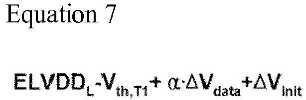
- In Equation 7, the difference voltage ΔVinit represents a difference voltage between the high and low voltages initH and initL of the first driving signal Vinit.
- When the node voltage defined as the following Equation 7 is applied to the control electrode CE1 of the first transistor T1, the first transistor T1 is turned on based on the difference voltage ΔVinit. Then, the high voltage ELVDDH of the first power source signal ELVDD is applied to the first electrode E11 of the first transistor T1 and thus, a driving current corresponding to the data voltage applied to the first node N, may flow through the organic light emitting diode OLED.
- The second transistor T2 is turned off in response to the high voltage VGH of the n-th scan signal S(n) and the third transistor T3 is turned off in response to the high voltage VGH of the second driving signal Vcomp.
- Therefore, during the fourth period 'd', driving currents corresponding to data voltages applied to the plurality of pixels, may flow through organic light emitting diodes OLEDs in the plurality of pixels and thus, the organic light emitting diodes OLEDs in the plurality of pixels may simultaneously emit the light.
- According to this embodiment of the invention, the pixel circuit may include only three transistors and two capacitors and thus, an ultra high definition display may be easily designed using the pixel circuit. In addition, the compensating period in the frame period may be freely controlled and thus, sufficiently obtained. In addition, whether the organic light emitting diode emits or not the light may be controlled by adjusting a level of the first power source signal.
-
FIGS. 10 to 12 are circuit diagrams illustrating pixel circuits according to embodiments of the invention. - Referring to
FIG. 10 , a pixel circuit PC3 may include a first transistor T1, a second transistor T2, a third transistor T3, a first capacitor Cst, a second capacitor Cpr and an organic light emitting diode OLED. According to this embodiment, the second transistor T2 may have a dual gate structure to avoid a leakage current. - Each of the first, second and third transistors T1, T2 and T3 in the pixel circuit PC3 may be a N-type transistor. The pixel circuit PC3 having the N-type transistor may drive as the pixel circuit PC1 described in the previous embodiment referring to
FIGS. 2 and3 . - Alternatively, each of the first, second and third transistors T1, T2 and T3 in the pixel circuit PC3 may be an P-type transistor. The pixel circuit PC3 having the P-type transistor may drive as the pixel circuit PC2 described in the previous embodiment referring to
FIGS. 8 and9 . - Referring to
FIG. 11 , a pixel circuit PC4 may include a first transistor T1, a second transistor T2, a third transistor T3, a first capacitor Cst, a second capacitor Cpr and an organic light emitting diode OLED. According to this embodiment, the third transistor T3 may have a dual gate structure to avoid a leakage current. - Each of the first, second and third transistors T1, T2 and T3 in the pixel circuit PC4 may be a N-type transistor. The pixel circuit PC4 having the N-type transistor may drive as the pixel circuit PC1 described in the previous embodiment referring to
FIGS. 2 and3 . - Alternatively, each of the first, second and third transistors T1, T2 and T3 in the pixel circuit PC4 may be an P-type transistor. The pixel circuit PC4 having the P-type transistor may drive as the pixel circuit PC2 described in the previous embodiment referring to
FIGS. 8 and9 . - Referring to
FIG. 12 , a pixel circuit PC5 may include a first transistor T1, a second transistor T2, a third transistor T3, a first capacitor Cst, a second capacitor Cpr and an organic light emitting diode OLED. According to this embodiment, the second and third transistors T2 and T3 may have a dual gate structure to avoid a leakage current. - Each of the first, second and third transistors T1, T2 and T3 in the pixel circuit PC5 may be a N-type transistor. The pixel circuit PC5 having the N-type transistor may drive as the pixel circuit PC1 described in the previous embodiment referring to
FIGS. 2 and3 . - Alternatively, each of the first, second and third transistors T1, T2 and T3 in the pixel circuit PC5 may be an P-type transistor. The pixel circuit PC5 having the P-type transistor may drive as the pixel circuit PC2 described in the previous embodiment referring to
FIGS. 8 and9 . - According to this embodiment, the pixel circuit includes only three transistors and two capacitors and thus, an ultra high definition display may be easily designed using the pixel circuit. In addition, the length of the compensating period in the frame period may be freely controlled and thus, a sufficient compensating period is obtained. In addition, whether the organic light emitting diode emits or not the light may be controlled by adjusting a level of the first power source signal. In addition, the leakage current of the transistor may be avoided.
-
FIG. 13 is a plan view illustrating a display part of a display apparatus according to an embodiment of the invention. - Referring to
FIGS. 2 and13 , the pixel circuit may be formed in a pixel circuit area PA. Thus, the first voltage line VL1, the second voltage line VL2, the third voltage line VL3, the n-th scan line SLn, the m-th data line DLm, first transistor T1, the second transistor T2, the third transistor T3, the first capacitor Cst and the second capacitor Cpr may be formed in the pixel circuit area PA. - The first voltage line VL1 may transfer a first driving signal Vinit and extend in the first direction D1.
- The second voltage line VL2 may transfer a first power source signal ELVDD and extend in the first direction D1.
- The third voltage line VL3 may transfer a second driving signal Vcomp and extend in the second direction D2.
- The n-th scan line SLn may transfer an n-th scan signal S(n) and extend in the second direction D2.
- The m-th data line DLm may transfer a data voltage and extend in the first direction D1. The m-th data line DLm may be formed across a central area of the pixel circuit area PA.
- The first transistor T1 may include a control electrode CE1, a first electrode E11, and a second electrode E12. The control electrode CE1 may have an island shape and be formed in the central area of the pixel circuit area PA. The first electrode E11 may be defined in a portion area of the second voltage line VL2 which is connected to an active pattern ACT through a first contact part CH1. The second electrode E12 may be defined in a portion area of the second capacitor Cpr which is connected to the active pattern ACT through a second contact part CH2.
- The second transistor T2 may include a control electrode CE2, a first electrode E21, and a second electrode E22. The control electrode CE2 may be defined in a portion area of the n-th scan line SLn. The first electrode E21 may be defined as an electrode which is connected to the active pattern ACT through a third contact part CH3. The second electrode E22 may be defined in a portion area of the second capacitor Cpr which is connected to the active pattern ACT through the second contact part CH2. The first electrode E21 may be connected to the control electrode CE1 of the first transistor T1 through a fourth contact part CH4.
- The third transistor T3 may include a control electrode CE3, a first electrode E31, and a second electrode E32. The control electrode CE3 may be defined in a portion area of the third voltage line VL2. The first electrode E31 may be defined in a portion area of the third voltage line VL3 which is connected to the active pattern ACT through a fifth contact part CH5. The second electrode E32 may be defined in a portion area of the second capacitor Cpr which is connected to the active pattern ACT through the second contact part CH2.
- The third voltage line VL3 may be connected to the third voltage line VL3 which is formed in an adjacent pixel circuit area, through a connection line and a sixth contact part CH6.
- The first capacitor Cst may be defined in an overlapping area in which an electrode extending in the second direction D2 from the first voltage line VL1 overlaps with the control electrode CE1 of the first transistor T1.
- The second capacitor Cpr may be defined in an overlapping area in which an electrode having the island shape in the central area of the pixel circuit area PA overlaps with the m-th data line DLm. The second capacitor Cpr may overlap with the first capacitor Cst.
-
FIG. 14 is a cross-sectional view taken along a line I-I' ofFIG. 13 .FIGS. 15 to 19 are plan views illustrating a method of manufacturing of the display part according to an embodiment of the invention. - Referring to
FIGS. 2 ,14 and15 , the display part may include abase substrate 111. - The
base substrate 111 may include an insulation material. For example, thebase substrate 111 may include a glass, a transparent plastic, a transparent metal oxide, etc. - The active pattern ACT may be disposed on the
base substrate 111. The active pattern ACT may include silicon. Alternatively, the active pattern ACT may be formed of a semiconductor oxide including a binary compound (ABx), a ternary compound (ABxCy), a quaternary compound (ABxCyDz), etc. which contain indium, zinc, gallium, tin, titanium, aluminum, hafnium (Hf), zirconium (Zr), magnesium (Mg), etc. These compounds may be used alone or in combination thereof. - The active pattern ACT may include first to sixth areas a1, a2, a3, a4, a5 and a6. The first to sixth areas a1, a2, a3, a4, a5 and a6 may be doped with an impurity, and thus may have electrical conductivity higher than those of other regions of the active pattern ACT. The first to sixth areas a1, a2, a3, a4, a5 and a6 may be first and second electrodes of first, second and third transistors T1, T2 and T3. Boundaries between the first to sixth areas a1, a2, a3, a4, a5 and a6 may not be clearly defined and first to sixth areas a1, a2, a3, a4, a5 and a6 may be electrically connected to each other.
- A
gate insulating layer 112 may be disposed on the active pattern ACT. Thegate insulating layer 112 may include a silicon compound, metal oxide, etc. For example, the gate insulation layer may include silicon oxide, silicon nitride, silicon oxynitride, aluminum oxide, tantalum oxide, hafnium oxide, zirconium oxide, titanium oxide, etc., which may be used alone or in combination thereof. In one embodiment, thegate insulation layer 112 may have a multilayer structure including a silicon oxide layer and silicon nitride layer. - A first conductive pattern MET1 which is patterned from a first conductive layer, may be disposed on the
gate insulating layer 112. The first conductive layer may include metal, alloy, metal nitride, conductive metal oxide, transparent conductive material, etc., which may be used alone or in combination thereof. - The first conductive pattern MET1 may include the n-th scan line SLn, the control electrode CE2 of the second transistor T2, the third voltage line VL3, the control electrode CE3 of the third transistor T3, the control electrode CE1 of the first transistor T1, and the first capacitor electrode CSE1 of the first capacitor Cst.
- The n-th scan line SLn may extend in the second direction D2.
- The control electrode CE2 of the second transistor T2 may be defined in a portion area of the n-th scan line SLn.
- The third voltage line VL3 may be disposed in parallel with the n-th scan line SLn.
- The control electrode CE3 of the third transistor T3 may be defined in a portion area of the third voltage line VL3.
- The control electrode CE1 of the first transistor T1 may have an island shape and be disposed in a central area of the pixel circuit area PA.
- The first capacitor electrode CSE1 of the first capacitor Cst may be defined in a portion area of the control electrode CE1.
- Referring to
FIGS. 2 ,14 and16 , a first insulatinginterlayer 113 may be disposed on the first conductive pattern MET1. The first insulatinginterlayer 113 may be formed of a silicon oxide, a silicon nitride, a silicon oxynitride, and etc. These may be used alone or in combination with each other. - The pixel circuit area PA may include a third contact part CH3, a fourth contact part CH4 and a fifth contact part CH5. The
gate insulating layer 112 and the first insulatinginterlayer 113 are etched to form the third and fifth contact parts CH3 and CH5. The insulatinginterlayer 113 are etched to form the fourth contact part CH4. - A second conductive pattern MET2 which is patterned from a second conductive layer, may be disposed on the first insulating
interlayer 113. The second conductive layer metal, alloy, metal nitride, conductive metal oxide, transparent conductive material, etc., which may be used alone or in combination thereof. - The second conductive pattern MET2 may include the first voltage line VL1, a second capacitor electrode CSE2 of the first capacitor Cst, a first electrode E21 of the second transistor T2 and the first electrode E31 of the third transistor T3.
- The first voltage line VL1 may extend in the first direction D1. The second capacitor electrode CSE2 of the first capacitor Cst may extend in the second direction D2 from the first voltage line VL1. The first capacitor Cst may be defined by the first electrode CSE1 of the first conductive pattern MET1 and the second capacitor electrode CSE2 of the second conductive pattern MET2.
- A first end portion of the first electrode E21 may be connected to the active pattern ACT through the third contact part CH3 and a second end portion of the first electrode E21 may be connected to the control electrode CE1 of the first transistor T1 through the fourth contact part CH4.
- The first electrode E31 of the third transistor T3 may be defined in a portion area of the first voltage line VL1 and be connected to the active pattern ACT through the fifth contact part CH5.
- Referring to
FIGS. 2 ,14 and17 , a second insulatinginterlayer 114 may be disposed on the second conductive pattern MET2. The pixel circuit area PA may include a sixth contact part CH6 in which the first and secondinsulating interlayers - A third conductive pattern MET3 which is patterned from a third conductive layer, may be disposed on the second insulating
interlayer 114. The third conductive pattern MET3 may include the m-th data line DLm, a third capacitor electrode CPE1 of the second capacitor Cpr and a connection electrode EE. - The m-th data line DLm may extend in the first direction D1 and be disposed in the central area of the pixel circuit area PA.
- The third capacitor electrode CPE1 of the second capacitor Cpr may extend from the m-th data line DLm.
- The connection electrode EE may be connected to the third voltage line VL3 and a third voltage line VL3 which is disposed in an adjacent pixel circuit area, through the sixth contact part CH6.
- Referring to
FIGS. 2 ,14 and18 , a thirdinsulating interlayer 115 may be disposed on the third conductive pattern MET3. The pixel circuit area PA may include a first contact part CH1 and a second contact part CH2 in which thegate insulating layer 112, the first insulatinginterlayer 113, the second insulatinginterlayer 114 and the third insulatinginterlayer 115 are etched. - A fourth conductive pattern MET4 which is patterned from a fourth conductive layer may be disposed on the third insulating
interlayer 115. - The fourth conductive pattern MET4 may include the second voltage line VL2, the first electrode E11 of the first transistor T1, a fourth capacitor electrode CPE2 of the second capacitor Cpr, the second electrode E12 of the first transistor T1, the second electrode E22 of the second transistor T2 and the second electrode E32 of the third transistor T3.
- The second voltage line VL2 may extend in the first direction D1 and may define a width of the pixel circuit area PA in the first direction D1 together with a second voltage line VL2 in the adjacent pixel circuit area PA.
- The first electrode E11 of the first transistor T1 may be defined in a portion area of the second voltage line VL2 connected to the active pattern AC through the first contact part CH1.
- The fourth capacitor electrode CPE2 of the second capacitor Cpr may have an island shape and be disposed in the central area of the pixel circuit area PA. The second capacitor Cpr may be defined by the third capacitor electrode CPE1 of the third conductive pattern MET3 and the fourth capacitor electrode CPE2 of the fourth conductive pattern MET4.
- The second electrode E12 of the first transistor T1, the second electrode E22 of the second transistor T2 and the second electrode E32 of the third transistor T3 may respectively defined in portion areas of the fourth capacitor electrode CPE2 connected to the active pattern ACT through the second contact part CH2.
- Referring to
FIGS. 2 ,14 and19 , a fourth insulatinginterlayer 116 may be disposed on the fourth conductive pattern MET4. The fourth insulatinginterlayer 116 may be formed with a high thickness to sufficiently cover the fourth conductive pattern MET4. - The pixel circuit area PA may include a seventh contact part CH7 in which the fourth insulating
interlayer 116 is etched. - A first pixel electrode PE1 may be disposed on the fourth insulating
interlayer 116. The first pixel electrode PE1 may correspond to the anode electrode of the organic light emitting diode. - A
pixel defining layer 117 may be disposed on the fourth insulatinginterlayer 116 on which the first pixel electrode PE1 is formed. - The
pixel defining layer 117 may form an opening on a portion area of the first pixel electrode PE1, and the organic light emitting layer EL may be disposed in the opening. Thus, the organic light emitting layer EL may be on the first pixel electrode PE1 exposed through the opening of the pixel definedlayer 117. - A second pixel electrode PE2 may be disposed on the organic light emitting layer EL. The second pixel electrode PE2 may correspond to the cathode electrode of the organic light emitting diode. The second pixel electrode PE2 may be commonly disposed in the plurality of pixel circuit areas.
- According to embodiments of the invention, the pixel circuit may include only three transistors and two capacitors and thus, an ultra high definition display may be easily designed using the pixel circuit. In addition, the length of the compensating period in the frame period may be freely controlled and thus, a sufficient compensating period is obtained. In addition, whether the organic light emitting diode emits or not the light may be controlled by adjusting a level of the first power source signal.
- The foregoing description is illustrative of the inventive concept and is not to be construed as limiting thereof. Although a few embodiments of the inventive concept have been described, those skilled in the art will readily appreciate that many modifications are possible without materially departing from the novel teachings and advantages of the inventive concept. Accordingly, all such modifications are intended to be included within the scope of the inventive concept as defined in the claims. In the claims, means-plus-function clauses are intended to cover the structures described herein as performing the recited function and not only structural equivalents but also equivalent structures. Therefore, it is to be understood that the foregoing is illustrative of the inventive concept and is not to be construed as limited to the specific embodiments disclosed, and that modifications to the disclosed embodiments, as well as other embodiments, are intended to be included within the scope of the appended claims.
Claims (30)
- A display apparatus comprising:a plurality of pixels, wherein a pixel of the plurality of pixels comprises:a first capacitor connected between a first voltage line configured to receive a first driving signal and a first node;a first transistor comprising a control electrode connected to the first node, a first electrode connected to a second voltage line configured to receive a first power source signal and a second electrode connected to a second node;an organic light emitting diode comprising an anode electrode connected to the second node and a cathode electrode configured to receive a second power source signal;a second capacitor connected between an m-th data line and the second node (wherein, 'm' is a natural number); anda second transistor comprising a control electrode connected to an n-th scan line (wherein, 'n' is a natural number), a first electrode connected to the first node and a second electrode connected to the second node.
- A display apparatus according to claim 1, wherein the pixel further comprises:a third transistor comprising a control electrode connected to a third voltage line configured to receive a second driving signal, a first electrode connected to the first voltage line and a second electrode connected to the second node.
- A display apparatus according to claim 2, wherein each of the first, second and third transistors is an N-type transistor.
- A display apparatus according to claim 3, wherein during a first period of a frame period, the first voltage line is configured to receive a low voltage of a first driving signal, the second voltage line is configured to receive a high voltage of the first power source signal, the third voltage line is configured to receive a high voltage of the second driving signal and the n-th scan line is configured to receive a high voltage of a scan signal.
- A display apparatus according to claim 4, wherein during a second period of the frame period, the first voltage line is configured to receive a low voltage of the first driving signal, the second voltage line is configured to receive a low voltage of the first power source signal lower than the low voltage of the first driving signal, the third voltage line is configured to receive a low voltage of the second driving signal, and the n-th scan line is configured to receive a high voltage of the scan signal.
- A display apparatus according to claim 5, wherein during a third period of the frame period, the first voltage line is configured to receive a low voltage of the first driving signal, the second voltage line is configured to receive a high voltage of the first power source signal, the third voltage line is configured to receive a low voltage of the second driving signal, the n-th scan line receives a high voltage of the scan signal during an n-th horizontal period in the third period, and the m-th data line is configured to receive a data voltage corresponding to a plurality of horizontal lines.
- A display apparatus according to claim 6, wherein during the n-th horizontal period, a data voltage corresponding to an n-th horizontal line is divided by a voltage division ratio of the first and second capacitors which are connected in series and the divided voltage is applied to the first node.
- A display apparatus according to claim 6, wherein the m-th data line is configured to receive a reference voltage before the m-th data line receives a data voltage corresponding to a first horizontal line of a plurality of horizontal lines, and
the m-th data line is configured to receive a reference voltage after the m-th data line receives a data voltage corresponding to a last horizontal line of a plurality of horizontal lines. - A display apparatus according to claim 8, wherein the m-th data line is configured to receive a reference voltage before the first voltage line receives a high voltage of the first driving signal and,
the reference voltage is equal to or lower than a lowest voltage in a voltage range of the data voltage. - A display apparatus according to claim 6, wherein during a fourth period of the frame period, the first voltage line is configured to receive a high voltage of the first driving signal, the second voltage line is configured to receive a high voltage of the first power source signal, the third voltage line is configured to receive a low voltage of the second driving signal, and the n-th scan line is configured to receive a low voltage of the scan signal.
- A display apparatus according to claim 10, wherein when a difference voltage between the high voltage and the low voltage of the first driving signal is applied to the first node,
the first transistor is turned on and a driving current corresponding to the data voltage applied to the first node flows through the organic light emitting diode. - A display apparatus according to claim 2, wherein each of the first, second and third transistors is a P-type transistor.
- A display apparatus according to claim 12, wherein during a first period, the first voltage line is configured to receive a low voltage of the first driving signal, the second voltage line is configured to receive a low voltage of the first power source signal, the third voltage line is configured to receive a low voltage of the second driving signal, and the n-th scan line is configured to receive a low voltage of the scan signal.
- A display apparatus according to claim 13, wherein the low voltage of the first power source signal is higher than the low voltage of the first driving signal.
- A display apparatus according to claim 13, wherein during a second period of the frame period, the first voltage line is configured to receive a low voltage of the first driving signal, the second voltage line is configured to receive a low voltage of the first power source signal, the third voltage line is configured to receive a high voltage of the second driving signal and the n-th scan line is configured to receive a low voltage of the scan signal.
- A display apparatus according to claim 15, wherein during a third period of the fame period, the first voltage line is configured to receive a low voltage of the first driving signal, the second voltage line is configured to receive a low voltage of the first power source signal, the third voltage line is configured to receive a high voltage of the second driving signal, the n-th scan line is configured to receive a low voltage of the scan signal during an n-th horizontal period in the third period, and the m-th data line is configured to receive a data voltage corresponding to a plurality of horizontal lines.
- A display apparatus according to claim 16, wherein during the n-th horizontal period, a data voltage corresponding to an n-th horizontal line is divided by a voltage division ratio of the first and second capacitors which are connected in series and the divided voltage is applied to the first node.
- A display apparatus according to claim 16, wherein the m-th data line is configured to receive a reference voltage before the m-th data line receives a data voltage corresponding to a first horizontal line of a plurality of horizontal lines, and
the m-th data line is configured to receive a reference voltage after the m-th data line receives a data voltage corresponding to a last horizontal line of a plurality of horizontal lines. - A display apparatus according to claim 18, wherein the m-th data line is configured to receive a reference voltage before the first voltage line receives a high voltage of the first driving signal, and
the reference voltage is equal to or lower than a lowest voltage in a voltage range of the data voltage. - A display apparatus according to claim 16, wherein during a fourth period of the frame period, the first voltage line is configured to receive a high voltage of the first driving signal, the second voltage line is configured to receive a high voltage of the first power source signal, the third voltage line is configured to receive a high voltage of the second driving signal, and the n-th scan line is configured to receive a high voltage of the scan signal.
- A display apparatus according to claim 20, wherein when a difference voltage between the high voltage and the low voltage of the first driving signal is applied to the first node,
the first transistor is turned on and a driving current corresponding to the data voltage applied to the first node flows through the organic light emitting diode. - A display apparatus according to claim 2, wherein at least one of the second and third transistors has a dual gate structure.
- A display apparatus according to claim 1, wherein:a first insulating interlayer is disposed on the control electrode of the first transistor and a first electrode of the first capacitor, the first voltage line and the second electrode of the first capacitor which are disposed on the first insulating interlayer,a second insulating interlayer is disposed on the first voltage line and the second electrode of the first capacitor, the m-th data line and a first electrode of the second capacitor which are disposed on the second insulating interlayer, anda third insulating interlayer is disposed on the m-th data line and a first electrode of the second capacitor, the second voltage line and a second electrode of the second capacitor which are disposed on the third insulating interlayer.
- A method of driving a display apparatus comprising a plurality of pixels which respectively comprises an organic light emitting diode, the method comprising:applying a low voltage of a first driving signal to an anode electrode of the organic light emitting diode to initialize the anode electrode;applying a low voltage of a first power source signal to a first electrode of a first transistor to diode-connect the first transistor;dividing a data voltage applied to a data line using first and second capacitors which are connected in series to apply divided voltage to a control electrode of the first transistor; andapplying a high voltage of the first driving signal to the control electrode of the first transistor to emit a light from the organic light emitting diode.
- A method according to claim 24, wherein when the first transistor is an N-type transistor, the low voltage of the first power source signal is lower than the low voltage of the first driving signal, and
the low voltages of the first power source signal and the first driving signal are lower than a voltage of second power source signal applied to a cathode electrode of the organic light emitting diode. - A method according to claim 24, wherein when the first transistor is a P-type transistor, the low voltage of the first power source signal is higher than the low voltage of the first driving signal, and
the low voltages of the first power source signal and the first driving signal are lower than a voltage of second power source signal applied to a cathode electrode of the organic light emitting diode. - A method according to claim 24, wherein a difference between the high and low voltages of the first driving signal is applied to a control electrode of the first transistor, a high voltage of the first driving signal being preset based on a turn-on voltage of the first transistor.
- A method according to claim 24, further comprising:applying a reference voltage to a data line before the data line receives a data voltage corresponding to a first horizontal line of a plurality of horizontal lines, andapplying the reference voltage to the data line after the data line receives a data voltage corresponding to a last horizontal line of a plurality of horizontal lines.
- A method according to claim 28, wherein the data line receives the reference voltage before a control electrode of the first transistor receives the high voltage of the first driving signal.
- A method according to claim 24, wherein each of initializing the anode electrode, diode-coupling the first transistor and emitting the light from the organic light emitting diode is simultaneously performed in all pixels.
Applications Claiming Priority (1)
| Application Number | Priority Date | Filing Date | Title |
|---|---|---|---|
| KR1020160061093A KR102485572B1 (en) | 2016-05-18 | 2016-05-18 | Display apparatus and method of driving the same |
Publications (3)
| Publication Number | Publication Date |
|---|---|
| EP3246913A2 true EP3246913A2 (en) | 2017-11-22 |
| EP3246913A3 EP3246913A3 (en) | 2017-12-06 |
| EP3246913B1 EP3246913B1 (en) | 2019-12-18 |
Family
ID=58715136
Family Applications (1)
| Application Number | Title | Priority Date | Filing Date |
|---|---|---|---|
| EP17171826.5A Active EP3246913B1 (en) | 2016-05-18 | 2017-05-18 | Display apparatus and method of driving the same |
Country Status (4)
| Country | Link |
|---|---|
| US (6) | US10311793B2 (en) |
| EP (1) | EP3246913B1 (en) |
| KR (1) | KR102485572B1 (en) |
| CN (1) | CN107403608B (en) |
Cited By (1)
| Publication number | Priority date | Publication date | Assignee | Title |
|---|---|---|---|---|
| EP4113499A1 (en) * | 2021-06-28 | 2023-01-04 | Samsung Display Co., Ltd. | Pixel and a display device including the same |
Families Citing this family (11)
| Publication number | Priority date | Publication date | Assignee | Title |
|---|---|---|---|---|
| KR102485572B1 (en) * | 2016-05-18 | 2023-01-09 | 삼성디스플레이 주식회사 | Display apparatus and method of driving the same |
| KR102367752B1 (en) | 2017-07-26 | 2022-03-02 | 삼성디스플레이 주식회사 | Organic Light Emitting Display Device and Driving Method Thereof |
| KR102498274B1 (en) * | 2017-12-06 | 2023-02-10 | 삼성디스플레이 주식회사 | Display apparatus and method of driving the same |
| KR102480426B1 (en) * | 2018-03-15 | 2022-12-22 | 삼성디스플레이 주식회사 | Display device and method for driving the same |
| KR102918010B1 (en) * | 2018-12-28 | 2026-01-27 | 엘지디스플레이 주식회사 | Display device |
| KR102734582B1 (en) * | 2019-03-25 | 2024-11-28 | 삼성디스플레이 주식회사 | Display device and driving method of the display device |
| CN110310603A (en) * | 2019-07-09 | 2019-10-08 | 京东方科技集团股份有限公司 | A kind of pixel-driving circuit and its driving method, display panel, display device |
| KR102921909B1 (en) * | 2019-08-08 | 2026-02-03 | 삼성디스플레이 주식회사 | Organic light emitting diode display device |
| KR102715313B1 (en) | 2019-11-18 | 2024-10-14 | 삼성디스플레이 주식회사 | Display panel |
| KR102712610B1 (en) | 2020-01-22 | 2024-10-04 | 삼성전자주식회사 | An electronic device including a display and a driving method of the display |
| CN112289267A (en) * | 2020-10-30 | 2021-01-29 | 昆山国显光电有限公司 | Pixel circuits and display panels |
Family Cites Families (20)
| Publication number | Priority date | Publication date | Assignee | Title |
|---|---|---|---|---|
| US7196699B1 (en) * | 1998-04-28 | 2007-03-27 | Sharp Kabushiki Kaisha | Latch circuit, shift register circuit, logical circuit and image display device operated with a low consumption of power |
| KR100698681B1 (en) * | 2004-06-29 | 2007-03-23 | 삼성에스디아이 주식회사 | Light emitting display |
| JP4160032B2 (en) * | 2004-09-01 | 2008-10-01 | シャープ株式会社 | Display device and driving method thereof |
| US20080136795A1 (en) | 2005-03-25 | 2008-06-12 | Takaji Numao | Display Device and Driving Method Thereof |
| JP4240059B2 (en) | 2006-05-22 | 2009-03-18 | ソニー株式会社 | Display device and driving method thereof |
| KR100823199B1 (en) * | 2007-04-05 | 2008-04-18 | 삼성에스디아이 주식회사 | Organic light emitting display |
| KR101429711B1 (en) * | 2007-11-06 | 2014-08-13 | 삼성디스플레이 주식회사 | OLED display and driving method thereof |
| KR101341011B1 (en) * | 2008-05-17 | 2013-12-13 | 엘지디스플레이 주식회사 | Light emitting display |
| KR100926634B1 (en) * | 2008-05-26 | 2009-11-11 | 삼성모바일디스플레이주식회사 | Organic electroluminescent display |
| JP4582216B2 (en) * | 2008-07-12 | 2010-11-17 | ソニー株式会社 | Semiconductor device, display panel and electronic equipment |
| KR20100041085A (en) * | 2008-10-13 | 2010-04-22 | 삼성모바일디스플레이주식회사 | Organic light emitting display device and driving method thereof |
| KR101056428B1 (en) * | 2009-03-27 | 2011-08-11 | 삼성모바일디스플레이주식회사 | Thin film transistor, manufacturing method thereof, and organic light emitting display device comprising the same |
| KR101528147B1 (en) * | 2011-10-14 | 2015-06-12 | 엘지디스플레이 주식회사 | Light emitting display device |
| KR101947810B1 (en) | 2012-08-22 | 2019-02-13 | 엘지디스플레이 주식회사 | Organic light emitting display device |
| KR101970574B1 (en) | 2012-12-28 | 2019-08-27 | 엘지디스플레이 주식회사 | Organic light emitting diode display device |
| CN105830143B (en) * | 2013-12-19 | 2018-11-23 | 夏普株式会社 | Display device and driving method thereof |
| KR102246342B1 (en) | 2014-06-26 | 2021-05-03 | 삼성전자주식회사 | Data storage device with multi-stack chip package and operating method thereof |
| KR102152690B1 (en) | 2014-06-26 | 2020-09-07 | 에스케이하이닉스 주식회사 | Latch circuit and semiconductor device including the same |
| KR102578715B1 (en) * | 2015-12-31 | 2023-09-18 | 엘지디스플레이 주식회사 | Organic light emitting diode display |
| KR102485572B1 (en) * | 2016-05-18 | 2023-01-09 | 삼성디스플레이 주식회사 | Display apparatus and method of driving the same |
-
2016
- 2016-05-18 KR KR1020160061093A patent/KR102485572B1/en active Active
-
2017
- 2017-01-06 US US15/400,465 patent/US10311793B2/en active Active
- 2017-05-15 CN CN201710337776.6A patent/CN107403608B/en active Active
- 2017-05-18 EP EP17171826.5A patent/EP3246913B1/en active Active
-
2019
- 2019-04-22 US US16/391,142 patent/US10733938B2/en active Active
-
2020
- 2020-06-23 US US16/908,803 patent/US11164525B2/en active Active
-
2021
- 2021-09-30 US US17/449,642 patent/US11610547B2/en active Active
-
2023
- 2023-03-20 US US18/123,334 patent/US12087228B2/en active Active
-
2024
- 2024-09-09 US US18/827,881 patent/US20240428739A1/en active Pending
Non-Patent Citations (1)
| Title |
|---|
| None |
Cited By (2)
| Publication number | Priority date | Publication date | Assignee | Title |
|---|---|---|---|---|
| EP4113499A1 (en) * | 2021-06-28 | 2023-01-04 | Samsung Display Co., Ltd. | Pixel and a display device including the same |
| US12207499B2 (en) | 2021-06-28 | 2025-01-21 | Samsung Display Co., Ltd. | Pixel and a display device including the same |
Also Published As
| Publication number | Publication date |
|---|---|
| US10311793B2 (en) | 2019-06-04 |
| US20200320936A1 (en) | 2020-10-08 |
| CN107403608A (en) | 2017-11-28 |
| US11610547B2 (en) | 2023-03-21 |
| US20220020331A1 (en) | 2022-01-20 |
| EP3246913A3 (en) | 2017-12-06 |
| US12087228B2 (en) | 2024-09-10 |
| US20190251906A1 (en) | 2019-08-15 |
| EP3246913B1 (en) | 2019-12-18 |
| KR102485572B1 (en) | 2023-01-09 |
| US11164525B2 (en) | 2021-11-02 |
| CN107403608B (en) | 2022-08-05 |
| KR20170130681A (en) | 2017-11-29 |
| US20230230546A1 (en) | 2023-07-20 |
| US20170337872A1 (en) | 2017-11-23 |
| US20240428739A1 (en) | 2024-12-26 |
| US10733938B2 (en) | 2020-08-04 |
Similar Documents
| Publication | Publication Date | Title |
|---|---|---|
| US12087228B2 (en) | Display apparatus having pixel including three transistors and two capacitors, and method of driving the same | |
| US11056058B2 (en) | Scan driver and display device having the same | |
| US9818345B2 (en) | Organic light emitting display device and method of driving thereof | |
| US10700146B2 (en) | Pixel and organic light-emitting display device having the same | |
| US9214506B2 (en) | Pixel unit driving circuit, method for driving pixel unit driving circuit and display device | |
| US9786222B2 (en) | Pixel circuit and organic light-emitting diode display including the same | |
| EP2889862B1 (en) | Organic light emitting display device and method for driving the same | |
| US8654041B2 (en) | Organic light emitting display device having more uniform luminance and method of driving the same | |
| US11587513B2 (en) | Emission driver, display apparatus including the same and method of driving display apparatus | |
| US20180190204A1 (en) | Scan driver and display device including the same | |
| EP2234093A1 (en) | Organic Light Emitting Display Device | |
| CN108231007A (en) | Display device and its driving method | |
| US20140368414A1 (en) | Capacitor, driving circuit comprising the capacitor, and display device comprising the driving circuit | |
| KR20180004370A (en) | Pixel and stage circuit and organic light emitting display device having the pixel and the stage circuit | |
| KR20180003390A (en) | Organic light emitting display device and driving method of the same | |
| US10777131B2 (en) | Pixel and organic light emitting display device including the same | |
| US8284124B2 (en) | Organic electroluminescent display device and driving method of the same | |
| CN108022960A (en) | Show substrate and include its display device | |
| KR20160074772A (en) | Organic light emitting display device and method for driving thereof | |
| US10937364B2 (en) | Display device and driving method thereof | |
| US20180197467A1 (en) | Circuit and method for driving amoled pixel |
Legal Events
| Date | Code | Title | Description |
|---|---|---|---|
| PUAI | Public reference made under article 153(3) epc to a published international application that has entered the european phase |
Free format text: ORIGINAL CODE: 0009012 |
|
| STAA | Information on the status of an ep patent application or granted ep patent |
Free format text: STATUS: THE APPLICATION HAS BEEN PUBLISHED |
|
| PUAL | Search report despatched |
Free format text: ORIGINAL CODE: 0009013 |
|
| AK | Designated contracting states |
Kind code of ref document: A2 Designated state(s): AL AT BE BG CH CY CZ DE DK EE ES FI FR GB GR HR HU IE IS IT LI LT LU LV MC MK MT NL NO PL PT RO RS SE SI SK SM TR |
|
| AX | Request for extension of the european patent |
Extension state: BA ME |
|
| AK | Designated contracting states |
Kind code of ref document: A3 Designated state(s): AL AT BE BG CH CY CZ DE DK EE ES FI FR GB GR HR HU IE IS IT LI LT LU LV MC MK MT NL NO PL PT RO RS SE SI SK SM TR |
|
| AX | Request for extension of the european patent |
Extension state: BA ME |
|
| RIC1 | Information provided on ipc code assigned before grant |
Ipc: G09G 3/3266 20160101ALN20171030BHEP Ipc: H01L 27/32 20060101ALN20171030BHEP Ipc: G09G 3/3233 20160101AFI20171030BHEP |
|
| STAA | Information on the status of an ep patent application or granted ep patent |
Free format text: STATUS: REQUEST FOR EXAMINATION WAS MADE |
|
| 17P | Request for examination filed |
Effective date: 20180531 |
|
| RBV | Designated contracting states (corrected) |
Designated state(s): AL AT BE BG CH CY CZ DE DK EE ES FI FR GB GR HR HU IE IS IT LI LT LU LV MC MK MT NL NO PL PT RO RS SE SI SK SM TR |
|
| STAA | Information on the status of an ep patent application or granted ep patent |
Free format text: STATUS: EXAMINATION IS IN PROGRESS |
|
| 17Q | First examination report despatched |
Effective date: 20180718 |
|
| GRAP | Despatch of communication of intention to grant a patent |
Free format text: ORIGINAL CODE: EPIDOSNIGR1 |
|
| STAA | Information on the status of an ep patent application or granted ep patent |
Free format text: STATUS: GRANT OF PATENT IS INTENDED |
|
| RIC1 | Information provided on ipc code assigned before grant |
Ipc: G09G 3/3233 20160101AFI20190611BHEP Ipc: H01L 27/32 20060101ALN20190611BHEP Ipc: G09G 3/3266 20160101ALN20190611BHEP |
|
| INTG | Intention to grant announced |
Effective date: 20190705 |
|
| GRAS | Grant fee paid |
Free format text: ORIGINAL CODE: EPIDOSNIGR3 |
|
| GRAA | (expected) grant |
Free format text: ORIGINAL CODE: 0009210 |
|
| STAA | Information on the status of an ep patent application or granted ep patent |
Free format text: STATUS: THE PATENT HAS BEEN GRANTED |
|
| AK | Designated contracting states |
Kind code of ref document: B1 Designated state(s): AL AT BE BG CH CY CZ DE DK EE ES FI FR GB GR HR HU IE IS IT LI LT LU LV MC MK MT NL NO PL PT RO RS SE SI SK SM TR |
|
| REG | Reference to a national code |
Ref country code: CH Ref legal event code: EP |
|
| REG | Reference to a national code |
Ref country code: DE Ref legal event code: R096 Ref document number: 602017009754 Country of ref document: DE |
|
| REG | Reference to a national code |
Ref country code: IE Ref legal event code: FG4D |
|
| REG | Reference to a national code |
Ref country code: AT Ref legal event code: REF Ref document number: 1215468 Country of ref document: AT Kind code of ref document: T Effective date: 20200115 |
|
| REG | Reference to a national code |
Ref country code: NL Ref legal event code: FP |
|
| PG25 | Lapsed in a contracting state [announced via postgrant information from national office to epo] |
Ref country code: BG Free format text: LAPSE BECAUSE OF FAILURE TO SUBMIT A TRANSLATION OF THE DESCRIPTION OR TO PAY THE FEE WITHIN THE PRESCRIBED TIME-LIMIT Effective date: 20200318 Ref country code: FI Free format text: LAPSE BECAUSE OF FAILURE TO SUBMIT A TRANSLATION OF THE DESCRIPTION OR TO PAY THE FEE WITHIN THE PRESCRIBED TIME-LIMIT Effective date: 20191218 Ref country code: SE Free format text: LAPSE BECAUSE OF FAILURE TO SUBMIT A TRANSLATION OF THE DESCRIPTION OR TO PAY THE FEE WITHIN THE PRESCRIBED TIME-LIMIT Effective date: 20191218 Ref country code: LV Free format text: LAPSE BECAUSE OF FAILURE TO SUBMIT A TRANSLATION OF THE DESCRIPTION OR TO PAY THE FEE WITHIN THE PRESCRIBED TIME-LIMIT Effective date: 20191218 Ref country code: LT Free format text: LAPSE BECAUSE OF FAILURE TO SUBMIT A TRANSLATION OF THE DESCRIPTION OR TO PAY THE FEE WITHIN THE PRESCRIBED TIME-LIMIT Effective date: 20191218 Ref country code: GR Free format text: LAPSE BECAUSE OF FAILURE TO SUBMIT A TRANSLATION OF THE DESCRIPTION OR TO PAY THE FEE WITHIN THE PRESCRIBED TIME-LIMIT Effective date: 20200319 Ref country code: NO Free format text: LAPSE BECAUSE OF FAILURE TO SUBMIT A TRANSLATION OF THE DESCRIPTION OR TO PAY THE FEE WITHIN THE PRESCRIBED TIME-LIMIT Effective date: 20200318 |
|
| REG | Reference to a national code |
Ref country code: LT Ref legal event code: MG4D |
|
| PG25 | Lapsed in a contracting state [announced via postgrant information from national office to epo] |
Ref country code: HR Free format text: LAPSE BECAUSE OF FAILURE TO SUBMIT A TRANSLATION OF THE DESCRIPTION OR TO PAY THE FEE WITHIN THE PRESCRIBED TIME-LIMIT Effective date: 20191218 Ref country code: RS Free format text: LAPSE BECAUSE OF FAILURE TO SUBMIT A TRANSLATION OF THE DESCRIPTION OR TO PAY THE FEE WITHIN THE PRESCRIBED TIME-LIMIT Effective date: 20191218 |
|
| PG25 | Lapsed in a contracting state [announced via postgrant information from national office to epo] |
Ref country code: AL Free format text: LAPSE BECAUSE OF FAILURE TO SUBMIT A TRANSLATION OF THE DESCRIPTION OR TO PAY THE FEE WITHIN THE PRESCRIBED TIME-LIMIT Effective date: 20191218 |
|
| PG25 | Lapsed in a contracting state [announced via postgrant information from national office to epo] |
Ref country code: EE Free format text: LAPSE BECAUSE OF FAILURE TO SUBMIT A TRANSLATION OF THE DESCRIPTION OR TO PAY THE FEE WITHIN THE PRESCRIBED TIME-LIMIT Effective date: 20191218 Ref country code: PT Free format text: LAPSE BECAUSE OF FAILURE TO SUBMIT A TRANSLATION OF THE DESCRIPTION OR TO PAY THE FEE WITHIN THE PRESCRIBED TIME-LIMIT Effective date: 20200513 Ref country code: CZ Free format text: LAPSE BECAUSE OF FAILURE TO SUBMIT A TRANSLATION OF THE DESCRIPTION OR TO PAY THE FEE WITHIN THE PRESCRIBED TIME-LIMIT Effective date: 20191218 Ref country code: RO Free format text: LAPSE BECAUSE OF FAILURE TO SUBMIT A TRANSLATION OF THE DESCRIPTION OR TO PAY THE FEE WITHIN THE PRESCRIBED TIME-LIMIT Effective date: 20191218 |
|
| PG25 | Lapsed in a contracting state [announced via postgrant information from national office to epo] |
Ref country code: SK Free format text: LAPSE BECAUSE OF FAILURE TO SUBMIT A TRANSLATION OF THE DESCRIPTION OR TO PAY THE FEE WITHIN THE PRESCRIBED TIME-LIMIT Effective date: 20191218 Ref country code: IS Free format text: LAPSE BECAUSE OF FAILURE TO SUBMIT A TRANSLATION OF THE DESCRIPTION OR TO PAY THE FEE WITHIN THE PRESCRIBED TIME-LIMIT Effective date: 20200418 Ref country code: SM Free format text: LAPSE BECAUSE OF FAILURE TO SUBMIT A TRANSLATION OF THE DESCRIPTION OR TO PAY THE FEE WITHIN THE PRESCRIBED TIME-LIMIT Effective date: 20191218 |
|
| REG | Reference to a national code |
Ref country code: DE Ref legal event code: R097 Ref document number: 602017009754 Country of ref document: DE |
|
| REG | Reference to a national code |
Ref country code: AT Ref legal event code: MK05 Ref document number: 1215468 Country of ref document: AT Kind code of ref document: T Effective date: 20191218 |
|
| PLBE | No opposition filed within time limit |
Free format text: ORIGINAL CODE: 0009261 |
|
| STAA | Information on the status of an ep patent application or granted ep patent |
Free format text: STATUS: NO OPPOSITION FILED WITHIN TIME LIMIT |
|
| PG25 | Lapsed in a contracting state [announced via postgrant information from national office to epo] |
Ref country code: DK Free format text: LAPSE BECAUSE OF FAILURE TO SUBMIT A TRANSLATION OF THE DESCRIPTION OR TO PAY THE FEE WITHIN THE PRESCRIBED TIME-LIMIT Effective date: 20191218 Ref country code: ES Free format text: LAPSE BECAUSE OF FAILURE TO SUBMIT A TRANSLATION OF THE DESCRIPTION OR TO PAY THE FEE WITHIN THE PRESCRIBED TIME-LIMIT Effective date: 20191218 |
|
| 26N | No opposition filed |
Effective date: 20200921 |
|
| PG25 | Lapsed in a contracting state [announced via postgrant information from national office to epo] |
Ref country code: AT Free format text: LAPSE BECAUSE OF FAILURE TO SUBMIT A TRANSLATION OF THE DESCRIPTION OR TO PAY THE FEE WITHIN THE PRESCRIBED TIME-LIMIT Effective date: 20191218 Ref country code: SI Free format text: LAPSE BECAUSE OF FAILURE TO SUBMIT A TRANSLATION OF THE DESCRIPTION OR TO PAY THE FEE WITHIN THE PRESCRIBED TIME-LIMIT Effective date: 20191218 |
|
| PG25 | Lapsed in a contracting state [announced via postgrant information from national office to epo] |
Ref country code: IT Free format text: LAPSE BECAUSE OF FAILURE TO SUBMIT A TRANSLATION OF THE DESCRIPTION OR TO PAY THE FEE WITHIN THE PRESCRIBED TIME-LIMIT Effective date: 20191218 Ref country code: CH Free format text: LAPSE BECAUSE OF NON-PAYMENT OF DUE FEES Effective date: 20200531 Ref country code: LI Free format text: LAPSE BECAUSE OF NON-PAYMENT OF DUE FEES Effective date: 20200531 Ref country code: MC Free format text: LAPSE BECAUSE OF FAILURE TO SUBMIT A TRANSLATION OF THE DESCRIPTION OR TO PAY THE FEE WITHIN THE PRESCRIBED TIME-LIMIT Effective date: 20191218 |
|
| PG25 | Lapsed in a contracting state [announced via postgrant information from national office to epo] |
Ref country code: PL Free format text: LAPSE BECAUSE OF FAILURE TO SUBMIT A TRANSLATION OF THE DESCRIPTION OR TO PAY THE FEE WITHIN THE PRESCRIBED TIME-LIMIT Effective date: 20191218 |
|
| REG | Reference to a national code |
Ref country code: BE Ref legal event code: MM Effective date: 20200531 |
|
| PG25 | Lapsed in a contracting state [announced via postgrant information from national office to epo] |
Ref country code: LU Free format text: LAPSE BECAUSE OF NON-PAYMENT OF DUE FEES Effective date: 20200518 |
|
| PG25 | Lapsed in a contracting state [announced via postgrant information from national office to epo] |
Ref country code: IE Free format text: LAPSE BECAUSE OF NON-PAYMENT OF DUE FEES Effective date: 20200518 |
|
| PG25 | Lapsed in a contracting state [announced via postgrant information from national office to epo] |
Ref country code: BE Free format text: LAPSE BECAUSE OF NON-PAYMENT OF DUE FEES Effective date: 20200531 |
|
| PG25 | Lapsed in a contracting state [announced via postgrant information from national office to epo] |
Ref country code: TR Free format text: LAPSE BECAUSE OF FAILURE TO SUBMIT A TRANSLATION OF THE DESCRIPTION OR TO PAY THE FEE WITHIN THE PRESCRIBED TIME-LIMIT Effective date: 20191218 Ref country code: MT Free format text: LAPSE BECAUSE OF FAILURE TO SUBMIT A TRANSLATION OF THE DESCRIPTION OR TO PAY THE FEE WITHIN THE PRESCRIBED TIME-LIMIT Effective date: 20191218 Ref country code: CY Free format text: LAPSE BECAUSE OF FAILURE TO SUBMIT A TRANSLATION OF THE DESCRIPTION OR TO PAY THE FEE WITHIN THE PRESCRIBED TIME-LIMIT Effective date: 20191218 |
|
| PG25 | Lapsed in a contracting state [announced via postgrant information from national office to epo] |
Ref country code: MK Free format text: LAPSE BECAUSE OF FAILURE TO SUBMIT A TRANSLATION OF THE DESCRIPTION OR TO PAY THE FEE WITHIN THE PRESCRIBED TIME-LIMIT Effective date: 20191218 |
|
| P01 | Opt-out of the competence of the unified patent court (upc) registered |
Effective date: 20230530 |
|
| PGFP | Annual fee paid to national office [announced via postgrant information from national office to epo] |
Ref country code: NL Payment date: 20250422 Year of fee payment: 9 |
|
| PGFP | Annual fee paid to national office [announced via postgrant information from national office to epo] |
Ref country code: DE Payment date: 20250422 Year of fee payment: 9 |
|
| PGFP | Annual fee paid to national office [announced via postgrant information from national office to epo] |
Ref country code: FR Payment date: 20250422 Year of fee payment: 9 |
|
| PGFP | Annual fee paid to national office [announced via postgrant information from national office to epo] |
Ref country code: GB Payment date: 20260324 Year of fee payment: 10 |