EP3246428A1 - Method for manufacturing metal carbonitride film or metalloid carbonitride film, metal carbonitride film or metalloid carbonitride film, and apparatus for manufacturing metal carbonitride film or metalloid carbonitride film - Google Patents
Method for manufacturing metal carbonitride film or metalloid carbonitride film, metal carbonitride film or metalloid carbonitride film, and apparatus for manufacturing metal carbonitride film or metalloid carbonitride film Download PDFInfo
- Publication number
- EP3246428A1 EP3246428A1 EP16737228.3A EP16737228A EP3246428A1 EP 3246428 A1 EP3246428 A1 EP 3246428A1 EP 16737228 A EP16737228 A EP 16737228A EP 3246428 A1 EP3246428 A1 EP 3246428A1
- Authority
- EP
- European Patent Office
- Prior art keywords
- carbonitride film
- metalloid
- metal
- film
- manufacturing
- Prior art date
- Legal status (The legal status is an assumption and is not a legal conclusion. Google has not performed a legal analysis and makes no representation as to the accuracy of the status listed.)
- Withdrawn
Links
- 0 *c1nc(*)n[n]1* Chemical compound *c1nc(*)n[n]1* 0.000 description 1
Images
Classifications
-
- C—CHEMISTRY; METALLURGY
- C23—COATING METALLIC MATERIAL; COATING MATERIAL WITH METALLIC MATERIAL; CHEMICAL SURFACE TREATMENT; DIFFUSION TREATMENT OF METALLIC MATERIAL; COATING BY VACUUM EVAPORATION, BY SPUTTERING, BY ION IMPLANTATION OR BY CHEMICAL VAPOUR DEPOSITION, IN GENERAL; INHIBITING CORROSION OF METALLIC MATERIAL OR INCRUSTATION IN GENERAL
- C23C—COATING METALLIC MATERIAL; COATING MATERIAL WITH METALLIC MATERIAL; SURFACE TREATMENT OF METALLIC MATERIAL BY DIFFUSION INTO THE SURFACE, BY CHEMICAL CONVERSION OR SUBSTITUTION; COATING BY VACUUM EVAPORATION, BY SPUTTERING, BY ION IMPLANTATION OR BY CHEMICAL VAPOUR DEPOSITION, IN GENERAL
- C23C16/00—Chemical coating by decomposition of gaseous compounds, without leaving reaction products of surface material in the coating, i.e. chemical vapour deposition [CVD] processes
- C23C16/22—Chemical coating by decomposition of gaseous compounds, without leaving reaction products of surface material in the coating, i.e. chemical vapour deposition [CVD] processes characterised by the deposition of inorganic material, other than metallic material
- C23C16/30—Deposition of compounds, mixtures or solid solutions, e.g. borides, carbides, nitrides
- C23C16/36—Carbonitrides
-
- C—CHEMISTRY; METALLURGY
- C07—ORGANIC CHEMISTRY
- C07F—ACYCLIC, CARBOCYCLIC OR HETEROCYCLIC COMPOUNDS CONTAINING ELEMENTS OTHER THAN CARBON, HYDROGEN, HALOGEN, OXYGEN, NITROGEN, SULFUR, SELENIUM OR TELLURIUM
- C07F7/00—Compounds containing elements of Groups 4 or 14 of the Periodic Table
- C07F7/02—Silicon compounds
- C07F7/08—Compounds having one or more C—Si linkages
- C07F7/10—Compounds having one or more C—Si linkages containing nitrogen having a Si-N linkage
-
- C—CHEMISTRY; METALLURGY
- C23—COATING METALLIC MATERIAL; COATING MATERIAL WITH METALLIC MATERIAL; CHEMICAL SURFACE TREATMENT; DIFFUSION TREATMENT OF METALLIC MATERIAL; COATING BY VACUUM EVAPORATION, BY SPUTTERING, BY ION IMPLANTATION OR BY CHEMICAL VAPOUR DEPOSITION, IN GENERAL; INHIBITING CORROSION OF METALLIC MATERIAL OR INCRUSTATION IN GENERAL
- C23C—COATING METALLIC MATERIAL; COATING MATERIAL WITH METALLIC MATERIAL; SURFACE TREATMENT OF METALLIC MATERIAL BY DIFFUSION INTO THE SURFACE, BY CHEMICAL CONVERSION OR SUBSTITUTION; COATING BY VACUUM EVAPORATION, BY SPUTTERING, BY ION IMPLANTATION OR BY CHEMICAL VAPOUR DEPOSITION, IN GENERAL
- C23C16/00—Chemical coating by decomposition of gaseous compounds, without leaving reaction products of surface material in the coating, i.e. chemical vapour deposition [CVD] processes
- C23C16/22—Chemical coating by decomposition of gaseous compounds, without leaving reaction products of surface material in the coating, i.e. chemical vapour deposition [CVD] processes characterised by the deposition of inorganic material, other than metallic material
- C23C16/30—Deposition of compounds, mixtures or solid solutions, e.g. borides, carbides, nitrides
- C23C16/34—Nitrides
- C23C16/345—Silicon nitride
-
- C—CHEMISTRY; METALLURGY
- C23—COATING METALLIC MATERIAL; COATING MATERIAL WITH METALLIC MATERIAL; CHEMICAL SURFACE TREATMENT; DIFFUSION TREATMENT OF METALLIC MATERIAL; COATING BY VACUUM EVAPORATION, BY SPUTTERING, BY ION IMPLANTATION OR BY CHEMICAL VAPOUR DEPOSITION, IN GENERAL; INHIBITING CORROSION OF METALLIC MATERIAL OR INCRUSTATION IN GENERAL
- C23C—COATING METALLIC MATERIAL; COATING MATERIAL WITH METALLIC MATERIAL; SURFACE TREATMENT OF METALLIC MATERIAL BY DIFFUSION INTO THE SURFACE, BY CHEMICAL CONVERSION OR SUBSTITUTION; COATING BY VACUUM EVAPORATION, BY SPUTTERING, BY ION IMPLANTATION OR BY CHEMICAL VAPOUR DEPOSITION, IN GENERAL
- C23C16/00—Chemical coating by decomposition of gaseous compounds, without leaving reaction products of surface material in the coating, i.e. chemical vapour deposition [CVD] processes
- C23C16/22—Chemical coating by decomposition of gaseous compounds, without leaving reaction products of surface material in the coating, i.e. chemical vapour deposition [CVD] processes characterised by the deposition of inorganic material, other than metallic material
- C23C16/30—Deposition of compounds, mixtures or solid solutions, e.g. borides, carbides, nitrides
- C23C16/42—Silicides
-
- C—CHEMISTRY; METALLURGY
- C23—COATING METALLIC MATERIAL; COATING MATERIAL WITH METALLIC MATERIAL; CHEMICAL SURFACE TREATMENT; DIFFUSION TREATMENT OF METALLIC MATERIAL; COATING BY VACUUM EVAPORATION, BY SPUTTERING, BY ION IMPLANTATION OR BY CHEMICAL VAPOUR DEPOSITION, IN GENERAL; INHIBITING CORROSION OF METALLIC MATERIAL OR INCRUSTATION IN GENERAL
- C23C—COATING METALLIC MATERIAL; COATING MATERIAL WITH METALLIC MATERIAL; SURFACE TREATMENT OF METALLIC MATERIAL BY DIFFUSION INTO THE SURFACE, BY CHEMICAL CONVERSION OR SUBSTITUTION; COATING BY VACUUM EVAPORATION, BY SPUTTERING, BY ION IMPLANTATION OR BY CHEMICAL VAPOUR DEPOSITION, IN GENERAL
- C23C16/00—Chemical coating by decomposition of gaseous compounds, without leaving reaction products of surface material in the coating, i.e. chemical vapour deposition [CVD] processes
- C23C16/44—Chemical coating by decomposition of gaseous compounds, without leaving reaction products of surface material in the coating, i.e. chemical vapour deposition [CVD] processes characterised by the method of coating
- C23C16/448—Chemical coating by decomposition of gaseous compounds, without leaving reaction products of surface material in the coating, i.e. chemical vapour deposition [CVD] processes characterised by the method of coating characterised by the method used for generating reactive gas streams, e.g. by evaporation or sublimation of precursor materials
- C23C16/4481—Chemical coating by decomposition of gaseous compounds, without leaving reaction products of surface material in the coating, i.e. chemical vapour deposition [CVD] processes characterised by the method of coating characterised by the method used for generating reactive gas streams, e.g. by evaporation or sublimation of precursor materials by evaporation using carrier gas in contact with the source material
-
- C—CHEMISTRY; METALLURGY
- C23—COATING METALLIC MATERIAL; COATING MATERIAL WITH METALLIC MATERIAL; CHEMICAL SURFACE TREATMENT; DIFFUSION TREATMENT OF METALLIC MATERIAL; COATING BY VACUUM EVAPORATION, BY SPUTTERING, BY ION IMPLANTATION OR BY CHEMICAL VAPOUR DEPOSITION, IN GENERAL; INHIBITING CORROSION OF METALLIC MATERIAL OR INCRUSTATION IN GENERAL
- C23C—COATING METALLIC MATERIAL; COATING MATERIAL WITH METALLIC MATERIAL; SURFACE TREATMENT OF METALLIC MATERIAL BY DIFFUSION INTO THE SURFACE, BY CHEMICAL CONVERSION OR SUBSTITUTION; COATING BY VACUUM EVAPORATION, BY SPUTTERING, BY ION IMPLANTATION OR BY CHEMICAL VAPOUR DEPOSITION, IN GENERAL
- C23C16/00—Chemical coating by decomposition of gaseous compounds, without leaving reaction products of surface material in the coating, i.e. chemical vapour deposition [CVD] processes
- C23C16/44—Chemical coating by decomposition of gaseous compounds, without leaving reaction products of surface material in the coating, i.e. chemical vapour deposition [CVD] processes characterised by the method of coating
- C23C16/455—Chemical coating by decomposition of gaseous compounds, without leaving reaction products of surface material in the coating, i.e. chemical vapour deposition [CVD] processes characterised by the method of coating characterised by the method used for introducing gases into reaction chamber or for modifying gas flows in reaction chamber
- C23C16/45523—Pulsed gas flow or change of composition over time
- C23C16/45525—Atomic layer deposition [ALD]
-
- C—CHEMISTRY; METALLURGY
- C23—COATING METALLIC MATERIAL; COATING MATERIAL WITH METALLIC MATERIAL; CHEMICAL SURFACE TREATMENT; DIFFUSION TREATMENT OF METALLIC MATERIAL; COATING BY VACUUM EVAPORATION, BY SPUTTERING, BY ION IMPLANTATION OR BY CHEMICAL VAPOUR DEPOSITION, IN GENERAL; INHIBITING CORROSION OF METALLIC MATERIAL OR INCRUSTATION IN GENERAL
- C23C—COATING METALLIC MATERIAL; COATING MATERIAL WITH METALLIC MATERIAL; SURFACE TREATMENT OF METALLIC MATERIAL BY DIFFUSION INTO THE SURFACE, BY CHEMICAL CONVERSION OR SUBSTITUTION; COATING BY VACUUM EVAPORATION, BY SPUTTERING, BY ION IMPLANTATION OR BY CHEMICAL VAPOUR DEPOSITION, IN GENERAL
- C23C16/00—Chemical coating by decomposition of gaseous compounds, without leaving reaction products of surface material in the coating, i.e. chemical vapour deposition [CVD] processes
- C23C16/44—Chemical coating by decomposition of gaseous compounds, without leaving reaction products of surface material in the coating, i.e. chemical vapour deposition [CVD] processes characterised by the method of coating
- C23C16/455—Chemical coating by decomposition of gaseous compounds, without leaving reaction products of surface material in the coating, i.e. chemical vapour deposition [CVD] processes characterised by the method of coating characterised by the method used for introducing gases into reaction chamber or for modifying gas flows in reaction chamber
- C23C16/45523—Pulsed gas flow or change of composition over time
- C23C16/45525—Atomic layer deposition [ALD]
- C23C16/45553—Atomic layer deposition [ALD] characterized by the use of precursors specially adapted for ALD
Definitions
- the present invention relates to a method for manufacturing a metal carbonitride film or a metalloid carbonitride film, a metal carbonitride film or a metalloid carbonitride film, and an apparatus for manufacturing a metal carbonitride film or a metalloid carbonitride film.
- a principal object of the present invention is to provide a method capable of manufacturing a metal carbonitride film or a metalloid carbonitride film at low temperature.
- a metal carbonitride film or a metalloid carbonitride film is formed using as a nitrogen source at least one of an N-trialkylsilyl-1,2,3-triazole compound and a 1,2,4-triazole compound represented by the following general formula (1): where Rs are the same or different, each represent a hydrogen atom, a linear, branched or cyclic alkyl group of 1 to 5 carbon atoms or a trialkylsilyl group of 1 to 5 carbon atoms, and, depending on circumstances, bond to each other to form a ring.
- a metal carbonitride film or a metalloid carbonitride film according to the present invention is one obtained by the method for manufacturing a metal carbonitride film or a metalloid carbonitride film according to the present invention.
- An apparatus for manufacturing a metal carbonitride film or a metalloid carbonitride film according to the present invention is an apparatus for manufacturing a metal carbonitride film or a metalloid carbonitride film for use in the method for manufacturing a metal carbonitride film or a metalloid carbonitride film according to the present invention.
- the apparatus for manufacturing a metal carbonitride film or a metalloid carbonitride film according to the present invention includes a reaction chamber, a metal or metalloid source supplying section, and a nitrogen source supplying section.
- the reaction chamber includes a placement section in which a film formation object is to be placed.
- the metal or metalloid source supplying section supplies a metal source or a metalloid source into the reaction chamber.
- the nitrogen source supplying section supplies the nitrogen source into the reaction chamber.
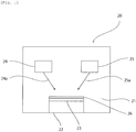
- Fig. 1 is a schematic view showing an apparatus for manufacturing a metal carbonitride film or a metalloid carbonitride film according to one embodiment of the present invention.
- a metal carbonitride film or a metalloid carbonitride film is formed using as a nitrogen source at least one of an N-trialkylsilyl-1,2,3-triazole compound and a 1,2,4-triazole compound represented by the following general formula (1): where Rs are the same or different, each represent a hydrogen atom, a linear, branched or cyclic alkyl group of 1 to 5 carbon atoms or a trialkylsilyl group of 1 to 5 carbon atoms, and, depending on circumstances, bond to each other to form a ring.
- a metal carbonitride film or a metalloid carbonitride film is formed on a film formation object by supplying a metal or metalloid source and at least one of an N-trialkylsilyl-1,2,3-triazole compound and a 1,2,4-triazole compound represented by the general formula (1).
- the formation of the metal carbonitride film or the metalloid carbonitride film can be suitably performed, for example, by the chemical vapor deposition process (hereinafter, referred to as the CVD process) or the atomic layer deposition process (hereinafter, referred to as the ALD process).
- a nitrogen source needs to be vaporized in order to form a film on a film formation object.
- a method for vaporizing the nitrogen source that can be used include not only a method for vaporizing the nitrogen source by filling or conveying the nitrogen source itself into a vaporizing chamber but also a method for vaporizing the nitrogen source by introducing a solution thereof diluted with a suitable solvent (for example, an aliphatic hydrocarbon, such as hexane, methylcyclohexane, ethylcyclohexane or octane; an aromatic hydrocarbon, such as toluene; or an ether, such as tetrahydrofuran or dibutyl ether) into a vaporizing chamber with a liquid conveying pump (solution method).
- a suitable solvent for example, an aliphatic hydrocarbon, such as hexane, methylcyclohexane, ethylcyclohexane or octane
- a film 26 is formed by supplying, to a film formation object 23 placed on a placement section 22 provided in a reaction chamber 21 of an apparatus 20 for manufacturing a metal carbonitride film or a metalloid carbonitride film, a metal or metalloid source 24a and a nitrogen source 25a from a metal or metalloid source supplying section 24 and a nitrogen source supplying section 25, respectively, provided inside the reaction chamber 21.
- the content of gas of the N-trialkylsilyl-1,2,3-triazole compound or the 1,2,4-triazole compound in the total amount of gas during vapor deposition of the metal carbonitride film or the metalloid carbonitride film is preferably 0.1% to 99% by volume and more preferably 0.5% to 95% by volume.
- the internal pressure in the reaction system during formation of the metal carbonitride film or the metalloid carbonitride film is preferably 1 Pa to 200 kPa and more preferably 10 Pa to 110 kPa.
- the temperature of the film formation object during formation of the metal carbonitride film or the metalloid carbonitride film is preferably 100 to 600°C and more preferably 200 to 500°C.
- the temperature for vaporizing the N-trialkylsilyl-1,2,3-triazole compound or the 1,2,4-triazole compound during formation of the metal carbonitride film or the metalloid carbonitride film is preferably 0°C to 180°C and more preferably 10°C to 100°C.
- the N-trialkylsilyl-1,2,3-triazole compound is at least one compound selected from the group consisting of compounds represented by the formulas (2) and (3) below.
- the compounds represented by the formulas (2) and (3) are tautomers. where R 1 s are the same or different, each represent a linear, branched or cyclic alkyl group of 1 to 3 carbon atoms, and, depending on circumstances, bond to each other to form a ring, and where R 2 s are the same or different, each represent a hydrogen atom, a linear, branched or cyclic alkyl group of 1 to 5 carbon atoms or a trialkylsilyl group of 1 to 5 carbon atoms, and, depending on circumstances, bond to each other to form a ring.
- linear or branched alkyl group of 1 to 3 carbon atoms examples include, for example, a methyl group, an ethyl group, an n-propyl group, an isopropyl group, and a cyclopropyl group.
- R 2 is a hydrogen atom, a linear, branched or cyclic alkyl group of 1 to 5 carbon atoms or a trialkylsilyl group of 1 to 5 carbon atoms.
- Examples of the linear, branched or cyclic alkyl group of 1 to 5 carbon atoms include, for example, a methyl group, an ethyl group, an n-propyl group, an isopropyl group, an n-butyl group, an isobutyl group, a t-butyl group, a pentyl group, a cyclopropyl group, a cyclobutyl group, and a cyclopentyl group.
- trialkylsilyl group of 1 to 5 carbon atoms examples include, for example, a trimethylsilyl group, a triethylsilyl group, a dimethylethylsilyl group, and a methyldiethylsilyl group.
- the plurality of R 2 s may bond to each other to form a ring and examples of the ring to be formed include, for example, saturated or unsaturated rings of 2 to 10 carbon atoms.
- N-trialkylsilyl-1,2,3-triazole compounds that can be preferably used in the present invention are represented, for example, by the formulas (4) to (27) below.
- the following N-trialkylsilyl-1,2,3-triazole compounds may be used alone or in combination of two or more of them.
- N-trialkylsilyl-1,2,3-triazole compound can be performed in accordance with a known method (see, for example, MAGNETIC RESONANCE IN CHEMISTRY, Vol. 36, 110, (1998 )). According to this, it is disclosed that N-trimethylsilyl-1,2,3-triazole formed by reaction between 1,2,3-triazole and hexamethyldisilazane (bis (trimethylsilyl) amine) is produced as a mixture of two kinds of compounds.
- the 1,2,4-triazole compound used in the present invention is a compound represented by the following formula (1): where Rs are the same or different, each represent a hydrogen atom, a linear, branched or cyclic alkyl group of 1 to 5 carbon atoms or a trialkylsilyl group of 1 to 5 carbon atoms, and, depending on circumstances, bond to each other to form a ring.
- Examples of the linear, branched or cyclic alkyl group of 1 to 5 carbon atoms include, for example, a methyl group, an ethyl group, an n-propyl group, an isopropyl group, an n-butyl group, an isobutyl group, a t-butyl group, a pentyl group, a cyclopropyl group, a cyclobutyl group, and a cyclopentyl group.
- trialkylsilyl group of 1 to 5 carbon atoms examples include, for example, a trimethylsilyl group, a triethylsilyl group, a dimethylethylsilyl group, and a methyldiethylsilyl group.
- the plurality of Rs may bond to each other to form a ring and examples of the ring to be formed include, for example, saturated or unsaturated rings of 2 to 10 carbon atoms.
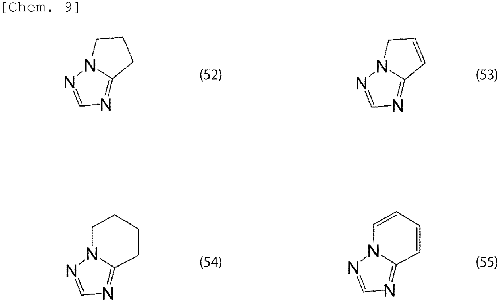
- 1,2,4-triazole compounds that can be preferably used in the present invention are represented, for example, by the formulas (28) to (55) below.
- the following 1,2,4-triazole compounds may be used alone or in combination of two or more of them.
- Metal Source or Metalloid Source Metal Source or Metalloid Source
- the metal source or metalloid source that is preferably used is, for example, a metal halide or a metalloid halide.
- metal halide examples include trichloroaluminum, tribromoaluminum, trifluoroaluminum, triiodoaluminum, tetrabromotitanium, tetrachlorotitanium, tetrafluorotitanium, tetraiodotitanium, tetrabromozirconium, tetrachlorozirconium, tetrafluorozirconium, tetraiodozirconium, tetrabromohafnium, tetrachlorohafnium, tetrafluorohafnium, tetraiodohafnium, pentachlorotantalum, pentachloromolybdenum, hexafluoromolybdenum, bis(cyclopentadienyl)dichloromolybdenum, hexachlorotungsten, hex
- metalloid halide examples include tetrachlorosilane, tetrafluorosilane, hexachlorodisilane, chloropentamethyldisilane, dichlorotetramethyldisilane, monochlorosilane, dichlorosilane, trichlorosilane, tetrabromogermanium, tetrachlorogermanium, tetraiodogermanium, tribromoboron, trichloroboron, trifluoroboron, and triiodoboron.
- the method for manufacturing a metal carbonitride film or a metalloid carbonitride film according to the present invention is suitable particularly for manufacturing a silicon carbonitride film.
- a nitrogen source needs to be vaporized in order to form a film on a film formation object.
- a method for vaporizing the nitrogen source that can be used include not only a method for vaporizing the nitrogen source by filling or conveying the nitrogen source itself into a vaporizing chamber but also a method for vaporizing the nitrogen source by introducing a solution thereof diluted with a suitable solvent (for example, an aliphatic hydrocarbon, such as hexane, methylcyclohexane, ethylcyclohexane or octane; an aromatic hydrocarbon, such as toluene; or an ether, such as tetrahydrofuran or dibutyl ether) into a vaporizing chamber with a liquid conveying pump (solution method).
- a suitable solvent for example, an aliphatic hydrocarbon, such as hexane, methylcyclohexane, ethylcyclohexane or octane
- Each film was formed on a 20 mmx20 mm substrate by the CVD process using the compound shown in Table 1 under the conditions shown in Table 1. Furthermore, the formed film was analyzed by XPS (X-ray Photoelectron Spectroscopy) to identify the film.
- XPS X-ray Photoelectron Spectroscopy
- Silicon source hexachlorodisilane Vaporization temperature of hexachlorodisilane; 30°C Flow rate of Ar carrier for hexachlorodisilane; 5ml/min.
- Substrate material SiO 2 /Si Substrate temperature; 500°C Internal pressure in reaction system; 3990Pa Vapor deposition time; 60 min.
- Example 2 N-trialkylsilyl-1,2,3-triazole compound; mixture of (4) and (5) Film thickness; 50nm XPS analysis; silicon carbonitride film Vaporization temperature of N-trialkylsilyl-1,2,3-triazole compound; 60°C Flow rate of Ar carrier for N-trialkylsilyl-1,2,3-triazole compound; 5ml/min. Silicon source; hexachlorodisilane Vaporization temperature of hexachlorodisilane; 30°C Flow rate of Ar carrier for hexachlorodisilane; 5ml/min.
- Silicon source hexachlorodisilane Vaporization temperature of hexachlorodisilane; 30°C Flow rate of Ar carrier for hexachlorodisilane; 5ml/min.
- Substrate material SiO 2 /Si Substrate temperature; 300°C Internal pressure in reaction system; 3990Pa Vapor deposition time; 60 min.
- Each film was formed on a 20 mm x 20 mm substrate by the CVD process using the compound shown in Table 2 under the conditions shown in Table 1. Furthermore, the formed film was analyzed by XPS (X-ray Photoelectron Spectroscopy) to identify the film.
- XPS X-ray Photoelectron Spectroscopy
- Silicon source hexachlorodisilane Vaporization temperature of hexachlorodisilane; 30°C Flow rate of Ar carrier for hexachlorodisilane; 5ml/min.
- Substrate material SiO 2 /Si Substrate temperature; 500°C Internal pressure in reaction system; 3990Pa Vapor deposition time; 60 min.
- Silicon source hexachlorodisilane Vaporization temperature of hexachlorodisilane; 30°C Flow rate of Ar carrier for hexachlorodisilane; 5ml/min.
- Substrate material SiO 2 /Si Substrate temperature; 350°C Internal pressure in reaction system; 3990Pa Vapor deposition time; 60 min.
- Example 6 1,2,4-triazole compound; (40) Film thickness; 300nm XPS analysis; silicon carbonitride film Vaporization temperature of 1,2,4-triazole compound; 100°C Flow rate of Ar carrier for 1,2,4-triazole compound; 5ml/min.
- Silicon source hexachlorodisilane Vaporization temperature of hexachlorodisilane; 30°C Flow rate of Ar carrier for hexachlorodisilane; 5ml/min.
- Substrate material SiO 2 /Si Substrate temperature; 500°C Internal pressure in reaction system; 3990Pa Vapor deposition time; 60 min.
- Example 7 1,2,4-triazole compound; (40) Film thickness; 100nm XPS analysis; silicon carbonitride film Vaporization temperature of 1,2,4-triazole compound; 100°C Flow rate of Ar carrier for 1,2,4-triazole compound; 5ml/min.
- Silicon source hexachlorodisilane Vaporization temperature of hexachlorodisilane; 30°C Flow rate of Ar carrier for hexachlorodisilane; 5ml/min.
- Substrate material SiO 2 /Si Substrate temperature; 350°C Internal pressure in reaction system; 3990Pa Vapor deposition time; 60 min.
- Example 8 1,2,4-triazole compound; (40) Film thickness; 50nm XPS analysis; silicon carbonitride film Vaporization temperature of 1,2,4-triazole compound; 100°C Flow rate of Ar carrier for 1,2,4-triazole compound; 5ml/min.
- Silicon source hexachlorodisilane Vaporization temperature of hexachlorodisilane; 30°C Flow rate of Ar carrier for hexachlorodisilane; 5ml/min.
- Substrate material SiO 2 /Si Substrate temperature; 250°C Internal pressure in reaction system; 3990Pa Vapor deposition time; 60 min.
Landscapes
- Chemical & Material Sciences (AREA)
- Organic Chemistry (AREA)
- General Chemical & Material Sciences (AREA)
- Chemical Kinetics & Catalysis (AREA)
- Engineering & Computer Science (AREA)
- Materials Engineering (AREA)
- Mechanical Engineering (AREA)
- Metallurgy (AREA)
- Inorganic Chemistry (AREA)
- Chemical Vapour Deposition (AREA)
- Formation Of Insulating Films (AREA)
Abstract
Provided is a method capable of manufacturing a metal carbonitride film or a metalloid carbonitride film at low temperature. A metal carbonitride film or a metalloid carbonitride film is formed using as a nitrogen source at least one of an N-trialkylsilyl-1,2,3-triazole compound and a 1,2,4-triazole compound represented by the following general formula (1):
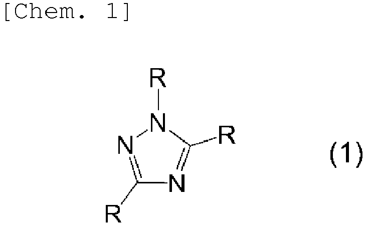
where Rs are the same or different, each represent a hydrogen atom, a linear, branched or cyclic alkyl group of 1 to 5 carbon atoms or a trialkylsilyl group of 1 to 5 carbon atoms, and, depending on circumstances, bond to each other to form a ring.
Description
- The present invention relates to a method for manufacturing a metal carbonitride film or a metalloid carbonitride film, a metal carbonitride film or a metalloid carbonitride film, and an apparatus for manufacturing a metal carbonitride film or a metalloid carbonitride film.
- Recently, in the fields of semiconductors, electronic components, and the like, much research and development has been done on highly chemical-resistant "carbonitride films in which carbon exists in metal nitride films or metalloid nitride films". As methods for manufacturing a metal carbonitride film or a metalloid carbonitride film, there are known, for example, a method for manufacturing it by combining an inorganic nitrogen gas, such as ammonia, and a hydrocarbon gas, such as acetylene (see, for example, Patent Literature 1) and a method in which isopropylamine is used as a supply source of carbon and nitrogen (carbonitriding agent) (see, for example, Patent Literature 2).
- Furthermore, there are disclosed methods in which aminosilane (see, for example, Patent Literatures 3 to 5) is used as a carbonitriding agent for manufacturing a silicon carbonitride film.
-
- Patent Literature 1:
JP-A-2007-189173 - Patent Literature 2:
JP-A-2009-283587 - Patent Literature 3:
JP-A-2014-177471 - Patent Literature 4:
JP-A-2010-267971 - Patent Literature 5:
JP-A-2010-43081 - However, in the method where an inorganic nitrogen gas and a hydrocarbon gas are used, there are problems, such as the necessity of separately providing respective means for supplying the respective gases and the necessity for high temperatures of 600°C or more during film formation.
- On the other hand, in the method where aminosilane is used, there is a problem that a substrate incapable of resisting plasma cannot be selected because the method is performed in a plasma atmosphere.
- A principal object of the present invention is to provide a method capable of manufacturing a metal carbonitride film or a metalloid carbonitride film at low temperature.
- In a method for manufacturing a metal carbonitride film or a metalloid carbonitride film according to the present invention, a metal carbonitride film or a metalloid carbonitride film is formed using as a nitrogen source at least one of an N-trialkylsilyl-1,2,3-triazole compound and a 1,2,4-triazole compound represented by the following general formula (1):

- A metal carbonitride film or a metalloid carbonitride film according to the present invention is one obtained by the method for manufacturing a metal carbonitride film or a metalloid carbonitride film according to the present invention.
- An apparatus for manufacturing a metal carbonitride film or a metalloid carbonitride film according to the present invention is an apparatus for manufacturing a metal carbonitride film or a metalloid carbonitride film for use in the method for manufacturing a metal carbonitride film or a metalloid carbonitride film according to the present invention. The apparatus for manufacturing a metal carbonitride film or a metalloid carbonitride film according to the present invention includes a reaction chamber, a metal or metalloid source supplying section, and a nitrogen source supplying section. The reaction chamber includes a placement section in which a film formation object is to be placed. The metal or metalloid source supplying section supplies a metal source or a metalloid source into the reaction chamber. The nitrogen source supplying section supplies the nitrogen source into the reaction chamber. Advantageous Effects of Invention
- According to the present invention, it is possible to provide a method capable of manufacturing a metal carbonitride film or a metalloid carbonitride film at low temperature. Brief Description of Drawings
- [
Fig. 1] Fig. 1 is a schematic view showing an apparatus for manufacturing a metal carbonitride film or a metalloid carbonitride film according to one embodiment of the present invention. - In a method for manufacturing a metal carbonitride film or a metalloid carbonitride film, a metal carbonitride film or a metalloid carbonitride film is formed using as a nitrogen source at least one of an N-trialkylsilyl-1,2,3-triazole compound and a 1,2,4-triazole compound represented by the following general formula (1):

- Specifically, a metal carbonitride film or a metalloid carbonitride film is formed on a film formation object by supplying a metal or metalloid source and at least one of an N-trialkylsilyl-1,2,3-triazole compound and a 1,2,4-triazole compound represented by the general formula (1). The formation of the metal carbonitride film or the metalloid carbonitride film can be suitably performed, for example, by the chemical vapor deposition process (hereinafter, referred to as the CVD process) or the atomic layer deposition process (hereinafter, referred to as the ALD process).
- In the CVD process and the ALD process, a nitrogen source needs to be vaporized in order to form a film on a film formation object. Examples of a method for vaporizing the nitrogen source that can be used include not only a method for vaporizing the nitrogen source by filling or conveying the nitrogen source itself into a vaporizing chamber but also a method for vaporizing the nitrogen source by introducing a solution thereof diluted with a suitable solvent (for example, an aliphatic hydrocarbon, such as hexane, methylcyclohexane, ethylcyclohexane or octane; an aromatic hydrocarbon, such as toluene; or an ether, such as tetrahydrofuran or dibutyl ether) into a vaporizing chamber with a liquid conveying pump (solution method).
- More specifically, as shown in
Fig. 1 , afilm 26 is formed by supplying, to afilm formation object 23 placed on aplacement section 22 provided in areaction chamber 21 of anapparatus 20 for manufacturing a metal carbonitride film or a metalloid carbonitride film, a metal ormetalloid source 24a and anitrogen source 25a from a metal or metalloidsource supplying section 24 and a nitrogensource supplying section 25, respectively, provided inside thereaction chamber 21. - The content of gas of the N-trialkylsilyl-1,2,3-triazole compound or the 1,2,4-triazole compound in the total amount of gas during vapor deposition of the metal carbonitride film or the metalloid carbonitride film is preferably 0.1% to 99% by volume and more preferably 0.5% to 95% by volume.
- The internal pressure in the reaction system during formation of the metal carbonitride film or the metalloid carbonitride film is preferably 1 Pa to 200 kPa and more preferably 10 Pa to 110 kPa. The temperature of the film formation object during formation of the metal carbonitride film or the metalloid carbonitride film is preferably 100 to 600°C and more preferably 200 to 500°C. The temperature for vaporizing the N-trialkylsilyl-1,2,3-triazole compound or the 1,2,4-triazole compound during formation of the metal carbonitride film or the metalloid carbonitride film is preferably 0°C to 180°C and more preferably 10°C to 100°C.
- The N-trialkylsilyl-1,2,3-triazole compound is at least one compound selected from the group consisting of compounds represented by the formulas (2) and (3) below. The compounds represented by the formulas (2) and (3) are tautomers.

where R2s are the same or different, each represent a hydrogen atom, a linear, branched or cyclic alkyl group of 1 to 5 carbon atoms or a trialkylsilyl group of 1 to 5 carbon atoms, and, depending on circumstances, bond to each other to form a ring. - Examples of the linear or branched alkyl group of 1 to 3 carbon atoms include, for example, a methyl group, an ethyl group, an n-propyl group, an isopropyl group, and a cyclopropyl group.
- In the formulas (2) and (3), R2 is a hydrogen atom, a linear, branched or cyclic alkyl group of 1 to 5 carbon atoms or a trialkylsilyl group of 1 to 5 carbon atoms.
- Examples of the linear, branched or cyclic alkyl group of 1 to 5 carbon atoms include, for example, a methyl group, an ethyl group, an n-propyl group, an isopropyl group, an n-butyl group, an isobutyl group, a t-butyl group, a pentyl group, a cyclopropyl group, a cyclobutyl group, and a cyclopentyl group.
- Examples of the trialkylsilyl group of 1 to 5 carbon atoms include, for example, a trimethylsilyl group, a triethylsilyl group, a dimethylethylsilyl group, and a methyldiethylsilyl group.
- The plurality of R2s may bond to each other to form a ring and examples of the ring to be formed include, for example, saturated or unsaturated rings of 2 to 10 carbon atoms.
- The N-trialkylsilyl-1,2,3-triazole compounds that can be preferably used in the present invention are represented, for example, by the formulas (4) to (27) below. The following N-trialkylsilyl-1,2,3-triazole compounds may be used alone or in combination of two or more of them.


- The manufacture of the N-trialkylsilyl-1,2,3-triazole compound can be performed in accordance with a known method (see, for example, MAGNETIC RESONANCE IN CHEMISTRY, Vol. 36, 110, (1998)). According to this, it is disclosed that N-trimethylsilyl-1,2,3-triazole formed by reaction between 1,2,3-triazole and hexamethyldisilazane (bis (trimethylsilyl) amine) is produced as a mixture of two kinds of compounds.
- The 1,2,4-triazole compound used in the present invention is a compound represented by the following formula (1):

- Examples of the linear, branched or cyclic alkyl group of 1 to 5 carbon atoms include, for example, a methyl group, an ethyl group, an n-propyl group, an isopropyl group, an n-butyl group, an isobutyl group, a t-butyl group, a pentyl group, a cyclopropyl group, a cyclobutyl group, and a cyclopentyl group.
- Examples of the trialkylsilyl group of 1 to 5 carbon atoms include, for example, a trimethylsilyl group, a triethylsilyl group, a dimethylethylsilyl group, and a methyldiethylsilyl group.
- The plurality of Rs may bond to each other to form a ring and examples of the ring to be formed include, for example, saturated or unsaturated rings of 2 to 10 carbon atoms.
- The 1,2,4-triazole compounds that can be preferably used in the present invention are represented, for example, by the formulas (28) to (55) below. The following 1,2,4-triazole compounds may be used alone or in combination of two or more of them.


- The metal source or metalloid source that is preferably used is, for example, a metal halide or a metalloid halide.
- Examples of the metal halide include trichloroaluminum, tribromoaluminum, trifluoroaluminum, triiodoaluminum, tetrabromotitanium, tetrachlorotitanium, tetrafluorotitanium, tetraiodotitanium, tetrabromozirconium, tetrachlorozirconium, tetrafluorozirconium, tetraiodozirconium, tetrabromohafnium, tetrachlorohafnium, tetrafluorohafnium, tetraiodohafnium, pentachlorotantalum, pentachloromolybdenum, hexafluoromolybdenum, bis(cyclopentadienyl)dichloromolybdenum, hexachlorotungsten, hexafluorotungsten, dibromocobalt, dichlorocobalt, difluorocobalt, diiodocobalt, dibromonickel, dichloronickel, diiodonickel, dibromomanganese, dichloromanganese, difluoromanganese, diiodomanganese, monobromocopper, dibromocopper, monochlorocopper, dichlorocopper, difluorocopper, diiodocopper, tribromogallium, trichlorogallium, trifluorogallium, triiodogallium, tribromobismuth, trichlorobismuth, trifluorobismuth, triiodobismuth, tribromoruthenium, trichlororuthenium, trifluororuthenium, trichlororhodium, dibromoplatinum, dichloroplatinum, tetrachloroplatinum, diiodoplatinum, dibromopalladium, dichloropalladium, diiodopalladium, triiodoruthenium, benzenedichlororuthenium, dibromozinc, dichlorozinc, difluorozinc, and diiodozinc.
- Examples of the metalloid halide include tetrachlorosilane, tetrafluorosilane, hexachlorodisilane, chloropentamethyldisilane, dichlorotetramethyldisilane, monochlorosilane, dichlorosilane, trichlorosilane, tetrabromogermanium, tetrachlorogermanium, tetraiodogermanium, tribromoboron, trichloroboron, trifluoroboron, and triiodoboron.
- The method for manufacturing a metal carbonitride film or a metalloid carbonitride film according to the present invention is suitable particularly for manufacturing a silicon carbonitride film.
- In the CVD process and the ALD process, a nitrogen source needs to be vaporized in order to form a film on a film formation object. Examples of a method for vaporizing the nitrogen source that can be used include not only a method for vaporizing the nitrogen source by filling or conveying the nitrogen source itself into a vaporizing chamber but also a method for vaporizing the nitrogen source by introducing a solution thereof diluted with a suitable solvent (for example, an aliphatic hydrocarbon, such as hexane, methylcyclohexane, ethylcyclohexane or octane; an aromatic hydrocarbon, such as toluene; or an ether, such as tetrahydrofuran or dibutyl ether) into a vaporizing chamber with a liquid conveying pump (solution method).
- Next, the present invention will be described in concrete terms with reference to examples but the scope of the invention is not limited to these examples.
- An amount of 8.68 g (125.7 mmol) of 1,2,3-triazole and 10.14 g(62.8 mmol) of hexamethyldisilazane were added into a 100 ml volume flask equipped with a stirrer, a thermometer, and a drip funnel and the mixture liquid was reacted at 145°C to 150°C for two hours with stirring.
- After the end of the reaction, the resultant reaction liquid was distilled under reduced pressure (at 120°C and 27 kPa) to obtain 16.07 g of N-trimethylsilyl-1,2,3-triazole as a clear, colorless liquid (isolated yield; 90%).
- The values of physical properties of N-trimethylsilyl-1,2,3-triazole were as follows: 1H-NMR (CDCl3, δ (ppm)); 0.55 (9H, s), 7.76 (2H, s)
- Each film was formed on a 20 mmx20 mm substrate by the CVD process using the compound shown in Table 1 under the conditions shown in Table 1. Furthermore, the formed film was analyzed by XPS (X-ray Photoelectron Spectroscopy) to identify the film.
[Table 1] Film Formation Conditions Characteristics of Silicon Carbonitride Film Example 1 N-trialkylsilyl-1,2,3-triazole compound; mixture of (4) and (5) Film thickness; 200nm XPS analysis; silicon carbonitride film Vaporization temperature of N-trialkylsilyl-1,2,3-triazole compound; 60°C Flow rate of Ar carrier for N-trialkylsilyl-1,2,3-triazole compound; 5ml/min. Silicon source; hexachlorodisilane Vaporization temperature of hexachlorodisilane; 30°C Flow rate of Ar carrier for hexachlorodisilane; 5ml/min. Substrate material; SiO2/Si Substrate temperature; 500°C Internal pressure in reaction system; 3990Pa Vapor deposition time; 60 min. Example 2 N-trialkylsilyl-1,2,3-triazole compound; mixture of (4) and (5) Film thickness; 50nm XPS analysis; silicon carbonitride film Vaporization temperature of N-trialkylsilyl-1,2,3-triazole compound; 60°C Flow rate of Ar carrier for N-trialkylsilyl-1,2,3-triazole compound; 5ml/min. Silicon source; hexachlorodisilane Vaporization temperature of hexachlorodisilane; 30°C Flow rate of Ar carrier for hexachlorodisilane; 5ml/min. Substrate material; SiO2/Si Substrate temperature; 400°C Internal pressure in reaction system; 3990Pa Vapor deposition time; 60 min. Example 3 N-trialkylsilyl-1,2,3-triazole compound; mixture of (4) and (5) Film thickness; 10nm XPS analysis; silicon carbonitride film Vaporization temperature of N-trialkylsilyl-1,2,3-triazole compound; 60°C Flow rate of Ar carrier for N-trialkylsilyl-1,2,3-triazole compound; 5ml/min. Silicon source; hexachlorodisilane Vaporization temperature of hexachlorodisilane; 30°C Flow rate of Ar carrier for hexachlorodisilane; 5ml/min. Substrate material; SiO2/Si Substrate temperature; 300°C Internal pressure in reaction system; 3990Pa Vapor deposition time; 60 min. - It can be seen from the results in Examples 1 to 3 that with the use of an N-trialkylsilyl-1,2,3-triazole compound, a silicon carbonitride film can be manufactured at low temperature.
- An amount of 5.00 g (72.4 mmol) of 1,2,4-triazole and 5.84 g(32.6 mmol) of hexamethyldisilazane were added into a 100 ml volume flask equipped with a stirrer, a thermometer, and a drip funnel and the mixture liquid was reacted at 145 to 150°C for four hours with stirring.
- After the end of the reaction, the resultant reaction liquid was distilled under reduced pressure (at 120°C and 6.7 kPa) to obtain 5.33 g of N-trimethylsilyl-1,2,4-triazole as a clear, colorless liquid (isolated yield; 52%).
- The values of physical properties of N-trimethylsilyl-1,2,4-triazole were as follows: 1H-NMR (CDCl3, δ (ppm)); 0.50 (9H, s), 8.09 (1H, s), 8.21 (1H, s)
- Each film was formed on a 20 mm x 20 mm substrate by the CVD process using the compound shown in Table 2 under the conditions shown in Table 1. Furthermore, the formed film was analyzed by XPS (X-ray Photoelectron Spectroscopy) to identify the film.
[Table 2] Film Formation Conditions Characteristics of Silicon Carbonitride Film Example 4 1,2,4-triazole compound; (28) Film thickness; 300nm XPS analysis; silicon carbonitride film Vaporization temperature of 1,2,4-triazole compound; 120°C Flow rate of Ar carrier for 1,2,4-triazole compound; 5ml/min. Silicon source; hexachlorodisilane Vaporization temperature of hexachlorodisilane; 30°C Flow rate of Ar carrier for hexachlorodisilane; 5ml/min. Substrate material; SiO2/Si Substrate temperature; 500°C Internal pressure in reaction system; 3990Pa Vapor deposition time; 60 min. Example 5 1,2,4-triazole compound; (28) Film thickness; 100nm XPS analysis; silicon carbonitride film Vaporization temperature of 1,2,4-triazole compound; 120°C Flow rate of Ar carrier for 1,2,4-triazole compound; 5ml/min. Silicon source; hexachlorodisilane Vaporization temperature of hexachlorodisilane; 30°C Flow rate of Ar carrier for hexachlorodisilane; 5ml/min. Substrate material; SiO2/Si Substrate temperature; 350°C Internal pressure in reaction system; 3990Pa Vapor deposition time; 60 min. Example 6 1,2,4-triazole compound; (40) Film thickness; 300nm XPS analysis; silicon carbonitride film Vaporization temperature of 1,2,4-triazole compound; 100°C Flow rate of Ar carrier for 1,2,4-triazole compound; 5ml/min. Silicon source; hexachlorodisilane Vaporization temperature of hexachlorodisilane; 30°C Flow rate of Ar carrier for hexachlorodisilane; 5ml/min. Substrate material; SiO2/Si Substrate temperature; 500°C Internal pressure in reaction system; 3990Pa Vapor deposition time; 60 min. Example 7 1,2,4-triazole compound; (40) Film thickness; 100nm XPS analysis; silicon carbonitride film Vaporization temperature of 1,2,4-triazole compound; 100°C Flow rate of Ar carrier for 1,2,4-triazole compound; 5ml/min. Silicon source; hexachlorodisilane Vaporization temperature of hexachlorodisilane; 30°C Flow rate of Ar carrier for hexachlorodisilane; 5ml/min. Substrate material; SiO2/Si Substrate temperature; 350°C Internal pressure in reaction system; 3990Pa Vapor deposition time; 60 min. Example 8 1,2,4-triazole compound; (40) Film thickness; 50nm XPS analysis; silicon carbonitride film Vaporization temperature of 1,2,4-triazole compound; 100°C Flow rate of Ar carrier for 1,2,4-triazole compound; 5ml/min. Silicon source; hexachlorodisilane Vaporization temperature of hexachlorodisilane; 30°C Flow rate of Ar carrier for hexachlorodisilane; 5ml/min. Substrate material; SiO2/Si Substrate temperature; 250°C Internal pressure in reaction system; 3990Pa Vapor deposition time; 60 min. - It can be seen from the results in Examples 4 to 8 that with the use of a 1,2,4-triazole compound, a silicon carbonitride film can be manufactured at low temperature.
-
- 20 apparatus for manufacturing a metal carbonitride film or a metalloid carbonitride film
- 21 reaction chamber
- 22 placement section
- 23 film formation object
- 24 metal or metalloid source supplying section
- 24a metal or metalloid source
- 25 nitrogen source supplying section
- 25a nitrogen source
- 26 film
Claims (12)
- A method for manufacturing a metal carbonitride film or a metalloid carbonitride film, the method comprising forming a metal carbonitride film or a metalloid carbonitride film using as a nitrogen source at least one of an N-trialkylsilyl-1,2,3-triazole compound and a 1,2,4-triazole compound represented by the following general formula (1):

- The method for manufacturing a metal carbonitride film or a metalloid carbonitride film according to claim 1, wherein the N-trialkylsilyl-1,2,3-triazole compound is at least one compound selected from the group consisting of compounds represented by the following formulas (2) and (3):

where R2s are the same or different, each represent a hydrogen atom, a linear, branched or cyclic alkyl group of 1 to 5 carbon atoms or a trialkylsilyl group of 1 to 5 carbon atoms, and, depending on circumstances, bond to each other to form a ring. - The method for manufacturing a metal carbonitride film or a metalloid carbonitride film according to claim 1 or 2, wherein a silicon carbonitride film is formed as the metalloid carbonitride film.
- The method for manufacturing a metal carbonitride film or a metalloid carbonitride film according to any one of claims 1 to 3, wherein a solution of at least one of an N-trialkylsilyl-1,2,3-triazole compound and a 1,2,4-triazole compound represented by the general formula (1) using as a solvent at least one selected from the group consisting of aliphatic hydrocarbons, aromatic hydrocarbons, and ethers is used as a supply source of nitrogen.
- The method for manufacturing a metal carbonitride film or a metalloid carbonitride film according to any one of claims 1 to 4, wherein a metal carbonitride film or a metalloid carbonitride film is formed on a film formation object by supplying a metal or metalloid source and at least one of an N-trialkylsilyl-1,2,3-triazole compound and a 1,2,4-triazole compound represented by the general formula (1).
- The method for manufacturing a metal carbonitride film or a metalloid carbonitride film according to claim 5, wherein a metal halide or a metalloid halide is supplied as the metal or metalloid source.
- The method for manufacturing a metal carbonitride film or a metalloid carbonitride film according to any one of claims 1 to 6, wherein a film formation temperature for the metal carbonitride film or the metalloid carbonitride film is below 600°C.
- The method for manufacturing a metal carbonitride film or a metalloid carbonitride film according to claim 7, wherein the film formation temperature for the metal carbonitride film or the metalloid carbonitride film is below 550°C.
- The method for manufacturing a metal carbonitride film or a metalloid carbonitride film according to claim 8, wherein the film formation temperature for the metal carbonitride film or the metalloid carbonitride film is not more than 500°C.
- A metal carbonitride film or metalloid carbonitride film obtained by the manufacturing method according to any one of claims 1 to 9.
- The metal carbonitride film or metalloid carbonitride film according to claim 10, wherein the metalloid is silicon.
- An apparatus for manufacturing a metal carbonitride film or a metalloid carbonitride film, the apparatus being for use in the method for manufacturing a metal carbonitride film or a metalloid carbonitride film according to any one of claims 1 to 11, the apparatus comprising:a reaction chamber including a placement section in which a film formation object is to be placed;a metal or metalloid source supplying section that supplies the metal source or the metalloid source into the reaction chamber; anda nitrogen source supplying section that supplies the nitrogen source into the reaction chamber.
Applications Claiming Priority (3)
| Application Number | Priority Date | Filing Date | Title |
|---|---|---|---|
| JP2015004617A JP2016130337A (en) | 2015-01-14 | 2015-01-14 | Method for producing metal or metalloid carbonitride film |
| JP2015015194A JP2016138325A (en) | 2015-01-29 | 2015-01-29 | Production method of metal or semimetal carbonitride film |
| PCT/JP2016/050050 WO2016114157A1 (en) | 2015-01-14 | 2016-01-04 | Method for manufacturing metal carbonitride film or metalloid carbonitride film, metal carbonitride film or metalloid carbonitride film, and apparatus for manufacturing metal carbonitride film or metalloid carbonitride film |
Publications (1)
| Publication Number | Publication Date |
|---|---|
| EP3246428A1 true EP3246428A1 (en) | 2017-11-22 |
Family
ID=56405704
Family Applications (1)
| Application Number | Title | Priority Date | Filing Date |
|---|---|---|---|
| EP16737228.3A Withdrawn EP3246428A1 (en) | 2015-01-14 | 2016-01-04 | Method for manufacturing metal carbonitride film or metalloid carbonitride film, metal carbonitride film or metalloid carbonitride film, and apparatus for manufacturing metal carbonitride film or metalloid carbonitride film |
Country Status (6)
| Country | Link |
|---|---|
| US (1) | US20170342551A1 (en) |
| EP (1) | EP3246428A1 (en) |
| KR (1) | KR20170105483A (en) |
| CN (1) | CN107075675A (en) |
| TW (1) | TW201634729A (en) |
| WO (1) | WO2016114157A1 (en) |
Families Citing this family (1)
| Publication number | Priority date | Publication date | Assignee | Title |
|---|---|---|---|---|
| CN110560125B (en) * | 2019-09-06 | 2020-10-27 | 北京交通大学 | Preparation method and application of N-g-C3N4 visible light catalytic material |
Family Cites Families (4)
| Publication number | Priority date | Publication date | Assignee | Title |
|---|---|---|---|---|
| US7361930B2 (en) * | 2005-03-21 | 2008-04-22 | Agilent Technologies, Inc. | Method for forming a multiple layer passivation film and a device incorporating the same |
| DE102005049393B4 (en) * | 2005-10-15 | 2019-08-08 | Kennametal Widia Produktions Gmbh & Co. Kg | Method for producing a coated substrate body, substrate body with a coating and use of the coated substrate body |
| JP5064296B2 (en) * | 2008-05-21 | 2012-10-31 | 東京エレクトロン株式会社 | Method and apparatus for forming silicon carbonitride film |
| US8557702B2 (en) * | 2009-02-02 | 2013-10-15 | Asm America, Inc. | Plasma-enhanced atomic layers deposition of conductive material over dielectric layers |
-
2016
- 2016-01-04 KR KR1020177013897A patent/KR20170105483A/en not_active Withdrawn
- 2016-01-04 WO PCT/JP2016/050050 patent/WO2016114157A1/en not_active Ceased
- 2016-01-04 CN CN201680003675.9A patent/CN107075675A/en active Pending
- 2016-01-04 US US15/528,770 patent/US20170342551A1/en not_active Abandoned
- 2016-01-04 EP EP16737228.3A patent/EP3246428A1/en not_active Withdrawn
- 2016-01-13 TW TW105100983A patent/TW201634729A/en unknown
Also Published As
| Publication number | Publication date |
|---|---|
| KR20170105483A (en) | 2017-09-19 |
| TW201634729A (en) | 2016-10-01 |
| WO2016114157A1 (en) | 2016-07-21 |
| US20170342551A1 (en) | 2017-11-30 |
| CN107075675A (en) | 2017-08-18 |
Similar Documents
| Publication | Publication Date | Title |
|---|---|---|
| US11725111B2 (en) | Compositions and processes for depositing carbon-doped silicon-containing films | |
| US12230496B2 (en) | Organoaminosilane precursors and methods for depositing films comprising same | |
| US9920077B2 (en) | Amine substituted trisilylamine and tridisilylamine compounds and synthesis methods thereof | |
| EP2669249B1 (en) | Method for depositing silicon-containing films using organoaminodisilane precursors | |
| US9200167B2 (en) | Alkoxyaminosilane compounds and applications thereof | |
| EP2574611B1 (en) | Halogenated Organoaminosilane Precursors and Methods for Depositing Films Comprising Same | |
| EP2669248B1 (en) | Organoaminodisilane precursors and methods for depositing films comprising same | |
| US12421603B2 (en) | Composition for high temperature atomic layer deposition of high quality silicon oxide thin films | |
| US20200111665A1 (en) | Composition for depositing silicon-containing thin film and method for manufacturing silicon-containing thin film using the same | |
| JP2020502044A (en) | Metal complexes containing cyclopentadienyl ligand | |
| CN106459098A (en) | Monoaminosilane compounds | |
| CN106414462A (en) | Diaminosilane compounds | |
| US11401166B2 (en) | Process for producing isomer enriched higher silanes | |
| US20170342551A1 (en) | Method for manufacturing metal carbonitride film or metalloid carbonitride film, metal carbonitride film or metalloid carbonitride film, and apparatus for manufacturing metal carbonitride film or metalloid carbonitride film | |
| US9677178B2 (en) | Alkoxyaminosilane compounds and applications thereof | |
| US20170247786A1 (en) | Method for producing metal carbonitride film or metalloid carbonitride film, metal carbonitride film or metalloid carbonitride film, and apparatus for producing metal carbonitride film or metalloid carbonitride film | |
| JP2016138325A (en) | Production method of metal or semimetal carbonitride film | |
| JP6565448B2 (en) | Method for producing aluminum oxide film and raw material for producing aluminum oxide film | |
| US20200115238A1 (en) | Process for producing isomer enriched higher silanes | |
| JP2016130337A (en) | Method for producing metal or metalloid carbonitride film | |
| CN120752245A (en) | Cyclodisilazane compound, composition for depositing silicon-containing film comprising the same, and method for manufacturing silicon-containing film using the same |
Legal Events
| Date | Code | Title | Description |
|---|---|---|---|
| PUAI | Public reference made under article 153(3) epc to a published international application that has entered the european phase |
Free format text: ORIGINAL CODE: 0009012 |
|
| 17P | Request for examination filed |
Effective date: 20170710 |
|
| AK | Designated contracting states |
Kind code of ref document: A1 Designated state(s): AL AT BE BG CH CY CZ DE DK EE ES FI FR GB GR HR HU IE IS IT LI LT LU LV MC MK MT NL NO PL PT RO RS SE SI SK SM TR |
|
| AX | Request for extension of the european patent |
Extension state: BA ME |
|
| STAA | Information on the status of an ep patent application or granted ep patent |
Free format text: STATUS: THE APPLICATION HAS BEEN WITHDRAWN |
|
| 18W | Application withdrawn |
Effective date: 20171107 |