EP3245664B1 - A non-conductive substrate with tracks formed by sand blasting - Google Patents
A non-conductive substrate with tracks formed by sand blasting Download PDFInfo
- Publication number
- EP3245664B1 EP3245664B1 EP16737136.8A EP16737136A EP3245664B1 EP 3245664 B1 EP3245664 B1 EP 3245664B1 EP 16737136 A EP16737136 A EP 16737136A EP 3245664 B1 EP3245664 B1 EP 3245664B1
- Authority
- EP
- European Patent Office
- Prior art keywords
- layer
- coating material
- conductive substrate
- conductive
- tracks
- Prior art date
- Legal status (The legal status is an assumption and is not a legal conclusion. Google has not performed a legal analysis and makes no representation as to the accuracy of the status listed.)
- Active
Links
Images



Classifications
-
- B—PERFORMING OPERATIONS; TRANSPORTING
- B24—GRINDING; POLISHING
- B24C—ABRASIVE OR RELATED BLASTING WITH PARTICULATE MATERIAL
- B24C3/00—Abrasive blasting machines or devices; Plants
- B24C3/32—Abrasive blasting machines or devices; Plants designed for abrasive blasting of particular work, e.g. the internal surfaces of cylinder blocks
- B24C3/322—Abrasive blasting machines or devices; Plants designed for abrasive blasting of particular work, e.g. the internal surfaces of cylinder blocks for electrical components
-
- B—PERFORMING OPERATIONS; TRANSPORTING
- B24—GRINDING; POLISHING
- B24C—ABRASIVE OR RELATED BLASTING WITH PARTICULATE MATERIAL
- B24C1/00—Methods for use of abrasive blasting for producing particular effects; Use of auxiliary equipment in connection with such methods
- B24C1/04—Methods for use of abrasive blasting for producing particular effects; Use of auxiliary equipment in connection with such methods for treating only selected parts of a surface, e.g. for carving stone or glass
-
- B—PERFORMING OPERATIONS; TRANSPORTING
- B24—GRINDING; POLISHING
- B24C—ABRASIVE OR RELATED BLASTING WITH PARTICULATE MATERIAL
- B24C11/00—Selection of abrasive materials or additives for abrasive blasts
-
- H—ELECTRICITY
- H05—ELECTRIC TECHNIQUES NOT OTHERWISE PROVIDED FOR
- H05K—PRINTED CIRCUITS; CASINGS OR CONSTRUCTIONAL DETAILS OF ELECTRIC APPARATUS; MANUFACTURE OF ASSEMBLAGES OF ELECTRICAL COMPONENTS
- H05K3/00—Apparatus or processes for manufacturing printed circuits
- H05K3/02—Apparatus or processes for manufacturing printed circuits in which the conductive material is applied to the surface of the insulating support and is thereafter removed from such areas of the surface which are not intended for current conducting or shielding
- H05K3/027—Apparatus or processes for manufacturing printed circuits in which the conductive material is applied to the surface of the insulating support and is thereafter removed from such areas of the surface which are not intended for current conducting or shielding the conductive material being removed by irradiation, e.g. by photons, alpha or beta particles
-
- H—ELECTRICITY
- H05—ELECTRIC TECHNIQUES NOT OTHERWISE PROVIDED FOR
- H05K—PRINTED CIRCUITS; CASINGS OR CONSTRUCTIONAL DETAILS OF ELECTRIC APPARATUS; MANUFACTURE OF ASSEMBLAGES OF ELECTRICAL COMPONENTS
- H05K2203/00—Indexing scheme relating to apparatus or processes for manufacturing printed circuits covered by H05K3/00
- H05K2203/02—Details related to mechanical or acoustic processing, e.g. drilling, punching, cutting, using ultrasound
- H05K2203/025—Abrading, e.g. grinding or sand blasting
-
- H—ELECTRICITY
- H05—ELECTRIC TECHNIQUES NOT OTHERWISE PROVIDED FOR
- H05K—PRINTED CIRCUITS; CASINGS OR CONSTRUCTIONAL DETAILS OF ELECTRIC APPARATUS; MANUFACTURE OF ASSEMBLAGES OF ELECTRICAL COMPONENTS
- H05K2203/00—Indexing scheme relating to apparatus or processes for manufacturing printed circuits covered by H05K3/00
- H05K2203/11—Treatments characterised by their effect, e.g. heating, cooling, roughening
- H05K2203/1126—Firing, i.e. heating a powder or paste above the melting temperature of at least one of its constituents
Definitions
- the present disclosure generally relates to a method for forming one or more tracks, on a non-conductive substrate, particularly for forming the tracks by sand blasting.
- a method for forming one or more tracks, on a non-conductive substrate, particularly for forming the tracks by sand blasting.
- Such a method according to the preamble of independent claim 1, is known from document US 3 240 624 A .
- LTCC devices are monolithic microelectronic devices. In these devices, the entire ceramic support structure and any conductive, resistive, and dielectric materials are fired in a kiln simultaneously.
- Typical LTCC devices include capacitors, inductors, resistors, transformers, and hybrid circuits.
- LTCC technology is also used for a multilayer packaging for the electronics industry, MEMS (microelectromechanical switches), microprocessor and RF (radio frequency) applications.
- LTCC technology as compared to other packaging technologies exhibits the advantage that the LTCC can be generally fired at temperatures below 1000°C. This can be attributed to the special composition of the LTCC material. Due to this low temperature, it is possible to cofire the LTCC with at least one material selected from a group consisting of conductive, semi-conductive, non-conductive materials, and combination thereof.
- LTCC may be used to fabricate microwave devices, such as microwave antennas that are compact and lightweight.
- the microwave devices are fabricated using the LTCC technology by printing conductive, semi-conductive, and non-conductive tracks (hereinafter referred to as 'track' or 'tracks') by using thick film screen printing method.
- Typical dimensions of the devices may range from about 50 microns to about 200 microns with a typical thickness in the range from about 10 microns to 30 microns.
- An object of the present disclosure is to provide a method for forming tracks on non-conductive substrates
- Yet another object of the present disclosure is to provide a non-conductive substrate with tracks formed thereon.
- the present disclosure envisages a method for forming one or more tracks on a non-conductive substrate according to independent claim 1.
- the layer of coating material can be selected from at least one group from the following:
- the stencil can be composed of a material that is resistant to the abrasive material such as steel, aluminum, copper, brass, FRP sheets and the like.
- the abrasive material is a mixture of alumina and glass; wherein the glass is composed of Bi 2 O 3 , V 2 O 5 , P 2 O 5 and SiO 2 such that the shrinkage and coefficient of thermal expansion of the mixture of alumina and glass is compatible with that of the non-conductive substrate (LTCC).
- LTCC non-conductive substrate
- the particle size of the abrasive material used to erode and/or remove the exposed layer of coating material can be in the range from 10 ⁇ m to 50 ⁇ m.
- the coefficients of thermal expansion of the abrasive material and the non-conductive substrate are substantially equal. More specifically, the difference in the thermal expansion coefficient of the abrasive material and the non-conductive substrate is equal to or less than 5 x 10 -6 /°C.
- the shrinkages of the abrasive material and the non-conductive substrate are substantially equal, whereby the difference in the shrinkage of the two is equal to or less than 0.5%.
- the film formed on the non-conductive substrate can have a thickness in the range from 10 ⁇ m to 30 ⁇ m.
- a non-conductive substrate with tracks formed is disclosed using the method as described herein.
- the present disclosure provides a method for forming one or more tracks on a non-conductive substrate that obviates one or more drawbacks of the conventional method.
- FIG. 1 that illustrates a flow chart 100 depicting the steps involved in the fabrication of the micron level tracks on the LTCC substrate using the method disclosed in accordance with an embodiment of the present disclosure.
- the method for forming track(s) on a non-conductive substrate comprises the following steps:
- a non-conductive substrate with tracks formed thereon wherein the tracks are formed by sand blasting method.
- the present disclosure envisages a non-conductive substrate with tracks formed thereon wherein the tracks are formed by sand blasting method, wherein the method comprises the following steps:
- the layer of coating material is formed by applying the paste and is dried to remove the solvent therefrom.
- At least the shrinkage and the coefficient of thermal expansion of the abrasive material that is used to abrade the layer of coating material formed on the non-conductive substrate are compatible with each other.
- the chemical composition of the abrasive material used to abrade the layer of coating material is compatible with that of the non-conductive substrate.
- the physical and chemical properties of the non-conductive substrate, the layer of coating material formed thereon, and the abrasive material, used to abrade the layer of coating material are compatible with each other.
- composition of the sand or the abrasive material used to abrade the layer of coating material has a very significant impact on the properties of the non-conductive substrates including the shrinkage and the coefficient of thermal expansion.
- the abrasive material that is propelled on the material to erode it does remove the material, but at the same time gets embedded in the non-conductive substrate. This changes the physical and chemical properties of the non-conductive substrate substantially, which is not desired.
- the change in the physical and chemical properties due to embedding of the abrasive particles may generate strain or stress in the LTCC tape that may fracture or break the LTCC tape or can deform the shape the LTCC tape during the step of co-firing.
- This is attributed to changes in the coefficient of the thermal expansion and shrinkage of the LTCC tape due to infusion or embedding to the abrasive particles during the step of abrading the layer of coating material formed on the non-conducting substrate (LTCC in this case).
- the inventors of the present disclosure envisaged that if the physical and chemical properties of the abrasive material or particles and that of the non-conducting substrate (LTCC) are compatible with each other, that is, if the physical and chemical properties of the abrasive material are chosen such that even on embedding of the abrasive material in the LTCC substrate the physical and chemical properties of the LTCC substrate are not changed substantially, the problem of strain or stress generation in the LTCC tape that may fracture or break the LTCC tape or deform the shape of the LTCC tape during the step of co-firing may be averted.
- LTCC non-conducting substrate
- the problem of strain or stress generation in the LTCC tape that may fracture or break the LTCC tape or deform the shape of the LTCC tape during the step of co-firing can be averted.
- the method for forming one or more tracks on a LTCC substrate comprises the following steps:
- the layer of coating material is formed by applying a paste of the material chosen from a group consisting of conductive material, semi-conductive material, non-conductive material and any combinations thereof. The paste is then dried to remove the solvent therefrom.
- the layer of coating material is formed by screen printing process.
- the layer of coating material is selected from a group of metals (or conductive materials) consisting of silver, copper, gold, aluminum, iron and combinations thereof.
- the layer of coating material is selected from a group of semi-conductive materials consisting of silicon, germanium binary ternary oxide semiconductors in the form of paste or photoresists.
- the layer of coating material is selected from a group of non-conductive materials consisting of glass dielectric oxides including binary, ternary, quaternary combinations in the form of paste, taper and/ or photoresist.
- the stencil is composed of a material that is resistant to the abrasive material such as steel, aluminum, copper, brass and FRP sheets.
- a proper contact between the non-conductive substrate with the layer of coating material applied thereon, and the stencil that is placed on the layer of coating material is essential. It is necessary that during the whole process of sandblasting the stencil remains in contact with and in place on the layer of coating material. In the event of failing to provide proper contact between the two, it is observed that improper track formation takes place.
- the non-conductive substrate or the LTCC tape is pushed towards the stencil by applying fluid pressure at a surface that is opposite to the operative face.
- the fluid may be a gas such as pressurized air or nitrogen.
- the distance between the sandblasting gun that emits the abrasive particles or material is placed at a suitable distance so as to achieve optimum particle speed that would be sufficient to abrade the layer of coating material while keeping non-conductive substrate intact.
- the desired speed of the abrasive particles may be achieved by controlling one of the following:
- the abraded non-conductive substrate with the tracks formed thereon is cleaned with a pressurized fluid such as air or nitrogen so as to remove the loose dust particles settled thereon after the process of sandblasting, before and after removal of the stencil.
- a pressurized fluid such as air or nitrogen
- the abraded and cleaned non-conductive substrate with the tracks formed thereon are then vacuum sealed in polyethylene bag (106), laminated, and cut into individual packages and are co-fired (107) to obtain the required final LTCC or non-conductive substrate with the tracks thereon.
- the abrasive material is a mixture of alumina and glass, wherein the glass is composed of Bi 2 O 3 , V 2 O 5 , P 2 O 5 and SiO 2 so that the shrinkage and coefficient of thermal expansion of the mixture of alumina and glass is compatible with that of the non-conductive substrate.
- the proportion of alumina -glass and the glass composition of the abrasive material particles is chosen so that the difference in the thermal expansion coefficient of the abrasive material and the non-conductive substrate is less than or equal to 5 x 10 -6 /°C.
- the proportion of alumina and glass and the glass composition of the abrasive material particles is chosen so that the difference in the shrinkage of the abrasive material and the non-conductive substrate is less than or equal to 0.5%.
- the abrasive material has a particle size in the range from 10 ⁇ m to 50 ⁇ m.
- the particle size depends on the thickness of the tracks to be formed and/or eroded on the non-conductive substrate.
- the layer of coating material has thickness in the range from 10 ⁇ m to 30 ⁇ m.
- the thickness of the LTCC tape is in the range from 100 ⁇ m to 250 ⁇ m.
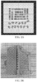
- FIG. 2A illustrates a photograph of a stencil
- FIG. 2B illustrates a photograph of a jig used for sandblasting, in accordance with an embodiment of the present disclosure, wherein the jig or stencil has patterns formed thereon that are complimentary to the tracks to be formed on non-conductive substrate with the paste.
- the tracks can be formed with at least one of the conductive, semi-conductive and non-conductive material applied thereon in the form of a layer of coating material.
- Precision laser cutting or any other method can be employed that is capable of providing sub-micron cutting accuracy from the stencil or jig.
- the jig and the stencil are made of steel.
- FIG. 3A is a photograph of conductive tracks obtained on the LTCC substrate by conventional screen printing method, wherein the conductive tracks of the conductive layer of coating material that are formed on the non-conductive substrate are blurred. This indicates that the screen printing method is not suitable for obtaining micron level precision.
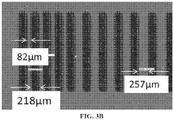
- FIG. 3B is a photograph of conductive tracks obtained on the LTCC substrate by the method of sandblasting or abrasive eroding as disclosed in accordance with the present disclosure, wherein the conductive tracks of the conductive layer of coating material that are formed on the non-conductive substrate are clear and sharp in contrast to that obtained by using the conventional screen printing technique.
- the presently disclosed method facilitates the formation of conductive tracks that are sharp, distinct and clear.
- FIG. 4A is a photograph of conductive tracks obtained on the LTCC substrate by the conventional screen printing method, wherein it is observed that the thickness of the conductive tracks that can be achieved using the conventional screen printing technique is 100 microns or above.
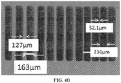
- FIG. 4B is a photograph of conductive tracks obtained on the LTCC substrate by the method of sandblasting or abrasive eroding as disclosed in accordance with the present disclosure, wherein the conductive track with 52 micron is achieved.
- FIG. 3B and 4B relate to photographic images of the 'conductive tracks' formed on the LTCC substrate by the sandblasting method as disclosed in accordance with the embodiments of the present disclosure
- similar tracks can be formed by using the method of sand blasting as disclosed in accordance with the embodiments of the present disclosure by applying a layer of coating of semi-conductive or non-conductive material or any possible combination of the conductive, semi-conductive and non-conductive material on the non-conductive substrate or LTCC substrate.
- the method for forming tracks on a non-conductive substrate in accordance with the present disclosure described herein above has several technical advantages including but not limited to the realization of conductive tracks on a non-conducting substrate, the method:
Landscapes
- Engineering & Computer Science (AREA)
- Mechanical Engineering (AREA)
- Manufacturing & Machinery (AREA)
- Microelectronics & Electronic Packaging (AREA)
- Manufacturing Of Printed Wiring (AREA)
- Electronic Switches (AREA)
- Apparatuses And Processes For Manufacturing Resistors (AREA)
Description
- The present disclosure generally relates to a method for forming one or more tracks, on a non-conductive substrate, particularly for forming the tracks by sand blasting. Such a method, according to the preamble of independent claim 1, is known from document
US 3 240 624 A . -
- Conductive track: herein means a conductive or electrical track or connector formed by using the presently disclosed method, by using an electrically conducting material.
- Semi-conductive track: herein means a semi-conductive track or connector formed by using the presently disclosed method, by using a semi-conducting material such as silicon.
- Non-conductive track: herein means a non-conductive track or connector formed by using the presently disclosed method, by using a non-conducting material such as non conducting polymers, glass-reinforced epoxy laminate sheet (FR4 sheets) /Glass Epoxy Fiberglass Sheets, and quartz or glass.
- FRP: fiber-reinforced plastic (FRP) herein refers to a composite material made of a polymer matrix reinforced with fibers. The fibers may include glass, carbon, basalt or aramid, but are not limited to these.
- Green Tape: as used herein refers to a low temperature co-fired ceramic (LTCC) material system from DuPont Microcircuit Materials (MCM) that provides the combined benefits of low sintering temperature co-fired glass-ceramic tape as a substrate for thick film.
- Shrinkage: as used herein means the change in the package dimensions (length, width and height) in percentage (%) after the sintering process, as compared to the green state package dimensions. The after firing dimensions are usually less than the before firing dimension due to agglomeration of crystalline materials and due to recrystallization of glass and evaporation of the organic part during the sintering process.
- Non-conducting substrate: herein means a base or mandrel that is electrically non-conducting or is made of an electrically non-conducting material.
- Stencil: herein means a mask or a sheet with a pattern cut out of it, such that when the stencil is placed on the layer of coating material that is applied on the non-conducting substrate and sand blasted, the unwanted portion of the layer of coating material is 'eroded' or 'removed' due to sand blasting whereas that portion of the layer of coating material remains intact on the substrate which corresponds to the desired track.
- Abrasive material: herein means the particles used to abrade or erode or remove the layer of coating material formed or disposed on the non-conductive substrate. The abrasive material is also referred to as sand or abrading material or particles.
- Low temperature co-fired ceramic (LTCC) devices are monolithic microelectronic devices. In these devices, the entire ceramic support structure and any conductive, resistive, and dielectric materials are fired in a kiln simultaneously. Typical LTCC devices include capacitors, inductors, resistors, transformers, and hybrid circuits.
- LTCC technology is also used for a multilayer packaging for the electronics industry, MEMS (microelectromechanical switches), microprocessor and RF (radio frequency) applications.
- LTCC technology as compared to other packaging technologies exhibits the advantage that the LTCC can be generally fired at temperatures below 1000°C. This can be attributed to the special composition of the LTCC material. Due to this low temperature, it is possible to cofire the LTCC with at least one material selected from a group consisting of conductive, semi-conductive, non-conductive materials, and combination thereof.
- In particular, LTCC may be used to fabricate microwave devices, such as microwave antennas that are compact and lightweight.
- Typically, the microwave devices are fabricated using the LTCC technology by printing conductive, semi-conductive, and non-conductive tracks (hereinafter referred to as 'track' or 'tracks') by using thick film screen printing method. Typical dimensions of the devices (such as antennas) may range from about 50 microns to about 200 microns with a typical thickness in the range from about 10 microns to 30 microns.
- In order to achieve the desired attenuation losses of the microwave devices (or circuit) it is necessary that the tracks formed have accurate dimension.
- It is observed that using the conventional screen printing technology for forming the tracks, the dimensional accuracy of the devices and/or the circuits is difficult to achieve.
- Further, it is observed that the method of forming tracks, using the conventional screen printing technique, inevitably necessitates control of one or more of the following factors including:
- environmental conditions;
- paste properties;
- operator skills; and
- paste and substrate interactions.
- These factors affect the reproducibility of the tracks and hence the device being fabricated.
- Thus, there is a need for providing a method of forming tracks on the LTCC substrate that obviates one or more disadvantages of the conventional screen printing technique. There is a need for providing a method that forms tracks that are reproducible. Further, there is a need for providing a method that facilitates in achieving the desired dimensional accuracy of the tracks being formed. Still further, there is a need for a method that does not necessitates control of one or more of the following factors including environmental conditions, paste properties, operator skills and paste and substrate interactions.
- Some of the objects of the present disclosure, which at least one embodiment herein satisfies are as follows:
It is an object of the present disclosure to ameliorate one or more problems of the prior art or to at least provide a useful alternative. - An object of the present disclosure is to provide a method for forming tracks on non-conductive substrates;
- Another object of the present disclosure is to provide a method for forming tracks on LTCC substrate;
- Still another object of the present disclosure is to provide a method for forming tracks on LTCC substrates with improved dimensional accuracy;
- Yet another object of the present disclosure is to provide a method for forming tracks on LTCC substrates that is not affected by ambient environmental conditions;
- Another object of the present disclosure is to provide a method for forming tracks on LTCC substrates that is independent of human operator skills;
- Still another object of the present disclosure is to provide a method for forming tracks on LTCC substrates that is not limited by the paste properties applied on it.
- Yet another object of the present disclosure is to provide a non-conductive substrate with tracks formed thereon.
- Other objects and advantages of the method of the present disclosure will be more apparent from the following description, which are not intended to limit the scope of the present disclosure.
- The present disclosure envisages a method for forming one or more tracks on a non-conductive substrate according to independent claim 1.
- The layer of coating material can be selected from at least one group from the following:
- a group of metals (or conductive materials) consisting of, but not limited to, silver, copper, gold, aluminum, iron and combinations thereof;
- a group of semi-conductive materials consisting of silicon, germanium binary ternary oxide semiconductors in the form of paste or photoresists
- a group of non-conductive materials consisting of dielectric oxides including binary, ternary, quaternary combinations in the form of paste, taper and/ or photoresist
- The stencil can be composed of a material that is resistant to the abrasive material such as steel, aluminum, copper, brass, FRP sheets and the like.
- The abrasive material is a mixture of alumina and glass; wherein the glass is composed of Bi2O3, V2O5, P2O5 and SiO2 such that the shrinkage and coefficient of thermal expansion of the mixture of alumina and glass is compatible with that of the non-conductive substrate (LTCC).
- Further, the particle size of the abrasive material used to erode and/or remove the exposed layer of coating material can be in the range from 10 µm to 50 µm.
- The coefficients of thermal expansion of the abrasive material and the non-conductive substrate are substantially equal. More specifically, the difference in the thermal expansion coefficient of the abrasive material and the non-conductive substrate is equal to or less than 5 x 10⁻⁶/°C.
- Alternatively or additionally, the shrinkages of the abrasive material and the non-conductive substrate are substantially equal, whereby the difference in the shrinkage of the two is equal to or less than 0.5%.
- The film formed on the non-conductive substrate can have a thickness in the range from 10 µm to 30 µm.
- In accordance with another embodiment of the present disclosure, a non-conductive substrate with tracks formed is disclosed using the method as described herein.
- The non-conductive substrate with the tracks fromed thereon and the method for forming one or more tracks on a non-conductive substrate will now be described with the help of the accompanying drawing in which:
-
FIG. 1 illustrates a flow chart depicting the steps involved in the fabrication of the micron level tracks on the LTCC substrate using the method disclosed in accordance with an embodiment of the present disclosure; -
FIG. 2A illustrates a photograph of a stencil used for sandblasting in accordance with an embodiment of the present disclosure; -
FIG. 2B illustrates a photograph of a jig used for sandblasting in accordance with an embodiment of the present disclosure; -
FIG. 3A illustrates a photograph of conductive tracks obtained on the LTCC substrate by conventional screen printing method; -
FIG. 3B illustrates a photograph of conductive tracks obtained on the LTCC substrate by the method of sandblasting or abrasive eroding as disclosed in accordance with the present disclosure; -
FIG. 4A illustrates a photograph of conductive tracks obtained on the LTCC substrate by the conventional screen printing method; and -
FIG. 4B illustrates a photograph of conductive tracks obtained on the LTCC substrate by the method of sandblasting or abrasive eroding as disclosed in accordance with the present disclosure, wherein a conductive track with 52 microns is achieved. - The non-conductive substrate with the tracks formed thereon and the method for forming one or more tracks on a non-conductive substrate of the present disclosure will now be described with reference to the embodiments, which do not limit the scope and ambit of the disclosure. The description provided is purely by way of example and illustration. The embodiment herein, the various features, and advantageous details thereof are explained with reference to the non-limiting embodiments in the following description. Descriptions of well-known components and processing techniques are omitted so as to not unnecessarily obscure the embodiments herein. The examples used herein are intended merely to facilitate an understanding of ways in which the embodiments herein may be practiced and to further enable those of skill in the art to practice the embodiments herein. Accordingly, the examples should not be construed as limiting the scope of the embodiments herein.
- The present disclosure provides a method for forming one or more tracks on a non-conductive substrate that obviates one or more drawbacks of the conventional method. Referring to
FIG. 1 that illustrates aflow chart 100 depicting the steps involved in the fabrication of the micron level tracks on the LTCC substrate using the method disclosed in accordance with an embodiment of the present disclosure. - In accordance with an embodiment of the present disclosure, the method for forming track(s) on a non-conductive substrate comprises the following steps:
- providing the non-conductive substrate (101);
- forming a layer of coating material on an operative face of the non-conductive substrate (102);
- disposing a stencil on the layer of coating material, thereby covering a selected portion of the layer of coating material while leaving exposed a portion of the layer of coating material corresponding to a pattern to be formed thus forming an assembly of the non-conductive substrate, the layer of coating material and the stencil (103);
- eroding the exposed portion of the layer of coating material by propelling an abrasive material using a blasting gun towards the assembly on the face on which the layer of coating material is formed and the stencil is disposed (104); and
- separating the stencil from the abraded assembly to obtain the desired tracks on the non-conducting substrate (105);
- In accordance with another embodiment of the present disclosure, a non-conductive substrate with tracks formed thereon is disclosed, wherein the tracks are formed by sand blasting method. In particular, the present disclosure envisages a non-conductive substrate with tracks formed thereon wherein the tracks are formed by sand blasting method, wherein the method comprises the following steps:
- providing the non-conductive substrate;
- forming a layer of coating material on an operative face of the non-conductive substrate;
- disposing a stencil on the layer of coating material, thereby covering a selected portion of the layer of coating material while leaving exposed a portion of the layer of coating material corresponding to a pattern to be formed thus forming an assembly of the non-conductive substrate, the layer of coating material and the stencil;
- eroding the exposed portion of the layer of coating material by propelling an abrasive material using a blasting gun towards the assembly on the face on which the layer of coating material is formed and the stencil is disposed; and
- separating the stencil from the abraded assembly to obtain the desired tracks on the non-conducting substrate;
- In accordance with the present disclosure, in the step of forming the layer of coating material on the operative face of the non-conductive substrate, the layer of coating material is formed by applying the paste and is dried to remove the solvent therefrom.
- In particular, in accordance with the present disclosure, at least the shrinkage and the coefficient of thermal expansion of the abrasive material that is used to abrade the layer of coating material formed on the non-conductive substrate are compatible with each other.
- Typically, the chemical composition of the abrasive material used to abrade the layer of coating material is compatible with that of the non-conductive substrate.
- In accordance with the present disclosure, the physical and chemical properties of the non-conductive substrate, the layer of coating material formed thereon, and the abrasive material, used to abrade the layer of coating material, are compatible with each other.
- It is observed that the composition of the sand or the abrasive material used to abrade the layer of coating material has a very significant impact on the properties of the non-conductive substrates including the shrinkage and the coefficient of thermal expansion.
- More specifically, the abrasive material that is propelled on the material to erode it, does remove the material, but at the same time gets embedded in the non-conductive substrate. This changes the physical and chemical properties of the non-conductive substrate substantially, which is not desired.
- In particular, for non-conducting substrates like that of LTCC the change in the physical and chemical properties due to embedding of the abrasive particles may generate strain or stress in the LTCC tape that may fracture or break the LTCC tape or can deform the shape the LTCC tape during the step of co-firing. This is attributed to changes in the coefficient of the thermal expansion and shrinkage of the LTCC tape due to infusion or embedding to the abrasive particles during the step of abrading the layer of coating material formed on the non-conducting substrate (LTCC in this case).
- The inventors of the present disclosure envisaged that if the physical and chemical properties of the abrasive material or particles and that of the non-conducting substrate (LTCC) are compatible with each other, that is, if the physical and chemical properties of the abrasive material are chosen such that even on embedding of the abrasive material in the LTCC substrate the physical and chemical properties of the LTCC substrate are not changed substantially, the problem of strain or stress generation in the LTCC tape that may fracture or break the LTCC tape or deform the shape of the LTCC tape during the step of co-firing may be averted.
- More specifically, if the shrinkage and the coefficient of the thermal expansion of the LTCC tape and that of the abrasive material grains or particles used to abrade the layer of coating material are similar, then the problem of strain or stress generation in the LTCC tape that may fracture or break the LTCC tape or deform the shape of the LTCC tape during the step of co-firing can be averted.
- In accordance with an embodiment of the present disclosure, the method for forming one or more tracks on a LTCC substrate comprises the following steps:
- providing the LTCC green tape substrate;
- forming a layer of coating material on an operative face of the LTCC green tape substrate;
- disposing a stencil on the layer of coating material thereby covering a selected portion of the layer of coating material while leaving exposed a portion of the layer of coating material corresponding to one or more tracks to be formed thus forming an assembly of the LTCC green tape substrate, the layer of coating material and the stencil;
- eroding the exposed portion of the layer of coating material by propelling an abrasive material using a blasting gun towards the assembly on the face on which the layer of coating material is formed and the stencil is disposed; and
- separating the stencil from the abraded assembly to obtain the desired tracks on the LTCC green tape substrate;
- In accordance with the present disclosure, in the step of forming the layer of coating material on the operative face of the LTCC green tape substrate, the layer of coating material is formed by applying a paste of the material chosen from a group consisting of conductive material, semi-conductive material, non-conductive material and any combinations thereof. The paste is then dried to remove the solvent therefrom.
- In accordance with the present disclosure, the layer of coating material is formed by screen printing process.
- In accordance with the present disclosure, the layer of coating material is selected from a group of metals (or conductive materials) consisting of silver, copper, gold, aluminum, iron and combinations thereof.
- In accordance with the present disclosure, the layer of coating material is selected from a group of semi-conductive materials consisting of silicon, germanium binary ternary oxide semiconductors in the form of paste or photoresists.
- In accordance with the present disclosure, the layer of coating material is selected from a group of non-conductive materials consisting of glass dielectric oxides including binary, ternary, quaternary combinations in the form of paste, taper and/ or photoresist.
- In accordance with the present disclosure, the stencil is composed of a material that is resistant to the abrasive material such as steel, aluminum, copper, brass and FRP sheets.
- In accordance with an embodiment of the present disclosure, it is observed that a proper contact between the non-conductive substrate with the layer of coating material applied thereon, and the stencil that is placed on the layer of coating material is essential. It is necessary that during the whole process of sandblasting the stencil remains in contact with and in place on the layer of coating material. In the event of failing to provide proper contact between the two, it is observed that improper track formation takes place.
- In order to achieve a proper contact without any gaps in between the layer of coating material and the stencil during the whole process of the sandblasting, the non-conductive substrate or the LTCC tape is pushed towards the stencil by applying fluid pressure at a surface that is opposite to the operative face. The fluid may be a gas such as pressurized air or nitrogen.
- Further, the distance between the sandblasting gun that emits the abrasive particles or material is placed at a suitable distance so as to achieve optimum particle speed that would be sufficient to abrade the layer of coating material while keeping non-conductive substrate intact.
- Still further, the desired speed of the abrasive particles may be achieved by controlling one of the following:
- distance between the sandblasting gun and the assembly of the stencil and non-conductive substrate with the layer of coating material; and
- the pressure of the fluid that facilitates in providing the required speed to the abrasive particles.
- In accordance with the present disclosure, after abrading the layer of coating material with the abrasive material using the sandblasting process the abraded non-conductive substrate with the tracks formed thereon is cleaned with a pressurized fluid such as air or nitrogen so as to remove the loose dust particles settled thereon after the process of sandblasting, before and after removal of the stencil.
- In accordance with the present disclosure, the abraded and cleaned non-conductive substrate with the tracks formed thereon are then vacuum sealed in polyethylene bag (106), laminated, and cut into individual packages and are co-fired (107) to obtain the required final LTCC or non-conductive substrate with the tracks thereon.
- The process of co-firing of the LTCC is well known in the art. For example, the DuPont™ Green Tape™ low temperature co-fired ceramic system Design and Layout Guidelines describes the conventional co-firing process of LTCC and is incorporated herein in its entirety.
- In accordance with the present disclosure, the abrasive material is a mixture of alumina and glass, wherein the glass is composed of Bi2O3, V2O5, P2O5 and SiO2 so that the shrinkage and coefficient of thermal expansion of the mixture of alumina and glass is compatible with that of the non-conductive substrate.
- In accordance with the present disclosure, the proportion of alumina -glass and the glass composition of the abrasive material particles is chosen so that the difference in the thermal expansion coefficient of the abrasive material and the non-conductive substrate is less than or equal to 5 x 10⁻⁶/°C.
- In accordance with the present disclosure, the proportion of alumina and glass and the glass composition of the abrasive material particles is chosen so that the difference in the shrinkage of the abrasive material and the non-conductive substrate is less than or equal to 0.5%.
- In accordance with the present disclosure, the abrasive material has a particle size in the range from 10 µm to 50 µm. The particle size depends on the thickness of the tracks to be formed and/or eroded on the non-conductive substrate.
- Typically, in accordance with the present disclosure, the layer of coating material has thickness in the range from 10 µm to 30 µm.
- Typically, the thickness of the LTCC tape is in the range from 100 µm to 250 µm.
- Further,
FIG. 2A illustrates a photograph of a stencil, whereasFIG. 2B illustrates a photograph of a jig used for sandblasting, in accordance with an embodiment of the present disclosure, wherein the jig or stencil has patterns formed thereon that are complimentary to the tracks to be formed on non-conductive substrate with the paste. The tracks can be formed with at least one of the conductive, semi-conductive and non-conductive material applied thereon in the form of a layer of coating material. Precision laser cutting or any other method can be employed that is capable of providing sub-micron cutting accuracy from the stencil or jig. In an exemplary embodiment of the present disclosure, the jig and the stencil are made of steel. -
FIG. 3A is a photograph of conductive tracks obtained on the LTCC substrate by conventional screen printing method, wherein the conductive tracks of the conductive layer of coating material that are formed on the non-conductive substrate are blurred. This indicates that the screen printing method is not suitable for obtaining micron level precision. -
FIG. 3B is a photograph of conductive tracks obtained on the LTCC substrate by the method of sandblasting or abrasive eroding as disclosed in accordance with the present disclosure, wherein the conductive tracks of the conductive layer of coating material that are formed on the non-conductive substrate are clear and sharp in contrast to that obtained by using the conventional screen printing technique. Thus, the presently disclosed method facilitates the formation of conductive tracks that are sharp, distinct and clear. -
FIG. 4A is a photograph of conductive tracks obtained on the LTCC substrate by the conventional screen printing method, wherein it is observed that the thickness of the conductive tracks that can be achieved using the conventional screen printing technique is 100 microns or above. -
FIG. 4B is a photograph of conductive tracks obtained on the LTCC substrate by the method of sandblasting or abrasive eroding as disclosed in accordance with the present disclosure, wherein the conductive track with 52 micron is achieved. - Though the
figures (3B and4B ) relate to photographic images of the 'conductive tracks' formed on the LTCC substrate by the sandblasting method as disclosed in accordance with the embodiments of the present disclosure, it is to be noted that similar tracks can be formed by using the method of sand blasting as disclosed in accordance with the embodiments of the present disclosure by applying a layer of coating of semi-conductive or non-conductive material or any possible combination of the conductive, semi-conductive and non-conductive material on the non-conductive substrate or LTCC substrate. - The method for forming tracks on a non-conductive substrate in accordance with the present disclosure described herein above has several technical advantages including but not limited to the realization of conductive tracks on a non-conducting substrate, the method:
- facilitates formation of tracks on non-conductive substrate which may be LTCC substrate;
- provides improved dimensional accuracy of the tracks formed on the substrate;
- is not affected by ambient environmental conditions;
- is independent of human operator skills;
- is not limited by the paste properties applied on it.
Claims (6)
- A method for forming one or more tracks on a non-conductive substrate, said method comprising the following steps:• forming a layer of coating material on an operative face of said non-conductive substrate;• disposing a stencil on said layer of coating material thereby covering a selected portion of said layer of coating material while leaving exposed a portion of said layer of coating material corresponding to a pattern to be formed thereby forming an assembly of said non-conductive substrate, said layer of coating material and said stencil;• eroding said exposed portion of said layer of coating material by propelling an abrasive material using a blasting gun towards said assembly on said operative face; and• separating said stencil from said abraded assembly;characterised in that said non-conductive substrate is low temperature co-fired ceramic (LTCC) and said abrasive material is a mixture of alumina and glass, wherein said glass is composed of Bi2O3, V2O5, P2O5 and SiO2 so that the shrinkage and coefficient of thermal expansion of said mixture of alumina and glass is compatible with that of said non-conductive substrate;
wherein said non-conductive substrate and said abrasive material has at least one of the following properties:• the difference in the thermal expansion coefficient between said non-conductive substrate and said abrasive material is equal to or less than 5 × 10⁻⁶/°C; and• the difference in the shrinkage between said non-conductive substrate and said abrasive material is equal to or less than 0.5%. - The method as claimed in claim 1, wherein said layer of coating material is selected from a group of conductive materials consisting of silver, copper, gold, aluminum, iron and combinations thereof.
- The method as claimed in claim 1, wherein said layer of coating material is selected from a group of semi-conductive materials consisting of silicon, germanium and combinations thereof.
- The method as claimed in claim 1, wherein said layer of coating material is selected from a group of non-conductive materials consisting of dielectric oxides including binary, ternary, quaternary combinations in the form of paste, tapes and/or photoresist quartz, glass and combinations thereof.
- The method as claimed in claim 1, wherein said stencil is composed of a material that is resistant to said abrasive material including steel, aluminum, copper, brass, non-conducting polymers, glass-reinforced epoxy laminate sheet, and glass epoxy fiberglass sheets.
- The method as claimed in claim 1, wherein said abrasive material has a particle size in the range from 10 µm to 50 µm; and
wherein said layer of coating material has a thickness in the range from 10 µm to 30 µm.
Applications Claiming Priority (2)
| Application Number | Priority Date | Filing Date | Title |
|---|---|---|---|
| IN130MU2015 | 2015-01-13 | ||
| PCT/IB2016/050083 WO2016113651A2 (en) | 2015-01-13 | 2016-01-08 | A non-conductive substrate with tracks formed by sand blasting |
Publications (3)
| Publication Number | Publication Date |
|---|---|
| EP3245664A2 EP3245664A2 (en) | 2017-11-22 |
| EP3245664A4 EP3245664A4 (en) | 2018-09-12 |
| EP3245664B1 true EP3245664B1 (en) | 2021-07-21 |
Family
ID=56406535
Family Applications (1)
| Application Number | Title | Priority Date | Filing Date |
|---|---|---|---|
| EP16737136.8A Active EP3245664B1 (en) | 2015-01-13 | 2016-01-08 | A non-conductive substrate with tracks formed by sand blasting |
Country Status (3)
| Country | Link |
|---|---|
| US (1) | US10335922B2 (en) |
| EP (1) | EP3245664B1 (en) |
| WO (1) | WO2016113651A2 (en) |
Families Citing this family (3)
| Publication number | Priority date | Publication date | Assignee | Title |
|---|---|---|---|---|
| US11577355B2 (en) * | 2017-12-29 | 2023-02-14 | The Boeing Company | Closed chamber abrasive flow machine systems and methods |
| US11707815B2 (en) * | 2019-07-09 | 2023-07-25 | General Electric Company | Creating 3D mark on protective coating on metal part using mask and metal part so formed |
| CN112312670A (en) * | 2020-11-05 | 2021-02-02 | 中国兵器工业集团第二一四研究所苏州研发中心 | Method for manufacturing high-precision micro-line radio frequency device |
Family Cites Families (17)
| Publication number | Priority date | Publication date | Assignee | Title |
|---|---|---|---|---|
| US2960417A (en) * | 1958-07-23 | 1960-11-15 | West Point Mfg Co | Multiple photocells and method of making same |
| US3240624A (en) * | 1962-03-07 | 1966-03-15 | Corning Glass Works | Method of forming a patterned electroconductive coating |
| US4232059A (en) * | 1979-06-06 | 1980-11-04 | E-Systems, Inc. | Process of defining film patterns on microelectronic substrates by air abrading |
| US4447519A (en) * | 1981-12-16 | 1984-05-08 | Nathan Pritikin | Solid photoresist and method of making photoresist |
| US5197234A (en) * | 1990-02-27 | 1993-03-30 | Gillenwater R Lee | Abrasive engraving process |
| US5069004A (en) * | 1990-02-27 | 1991-12-03 | Gillenwater R Lee | Abrasive engraving process |
| US5989689A (en) * | 1991-12-11 | 1999-11-23 | The Chromaline Corporation | Sandblast mask laminate with blastable pressure sensitive adhesive |
| US6047637A (en) * | 1999-06-17 | 2000-04-11 | Fujitsu Limited | Method of paste printing using stencil and masking layer |
| US6673522B2 (en) * | 2001-12-05 | 2004-01-06 | Plasmion Displays Llc | Method of forming capillary discharge site of plasma display panel using sand blasting |
| US7709766B2 (en) * | 2002-08-05 | 2010-05-04 | Research Foundation Of The State University Of New York | System and method for manufacturing embedded conformal electronics |
| GB2401485B (en) * | 2002-12-11 | 2006-07-26 | Dainippon Printing Co Ltd | Multilayer wiring board and manufacture method thereof |
| JP4361434B2 (en) * | 2003-08-29 | 2009-11-11 | 富士フイルム株式会社 | Mask, mask manufacturing method, and material processing method |
| US7444727B2 (en) * | 2006-03-10 | 2008-11-04 | Motorola, Inc. | Method for forming multi-layer embedded capacitors on a printed circuit board |
| US7367869B2 (en) * | 2006-05-02 | 2008-05-06 | U.S. Technology Corporation | Method of masking and a hot melt adhesive for use therewith |
| SG154342A1 (en) * | 2008-01-08 | 2009-08-28 | Opulent Electronics Internat P | Insulated metal substrate fabrication |
| JP5113114B2 (en) * | 2009-04-06 | 2013-01-09 | 新光電気工業株式会社 | Wiring board manufacturing method and wiring board |
| US20110052828A1 (en) * | 2009-09-03 | 2011-03-03 | Randy Allen Normann | Method for high-temperature ceramic circuits |
-
2016
- 2016-01-08 WO PCT/IB2016/050083 patent/WO2016113651A2/en not_active Ceased
- 2016-01-08 US US15/542,567 patent/US10335922B2/en active Active
- 2016-01-08 EP EP16737136.8A patent/EP3245664B1/en active Active
Non-Patent Citations (1)
| Title |
|---|
| None * |
Also Published As
| Publication number | Publication date |
|---|---|
| WO2016113651A2 (en) | 2016-07-21 |
| EP3245664A2 (en) | 2017-11-22 |
| US10335922B2 (en) | 2019-07-02 |
| WO2016113651A3 (en) | 2017-01-05 |
| EP3245664A4 (en) | 2018-09-12 |
| US20180264623A1 (en) | 2018-09-20 |
Similar Documents
| Publication | Publication Date | Title |
|---|---|---|
| US20180043618A1 (en) | Embedding apparatus and method utilizing additive manufacturing | |
| US20020174935A1 (en) | Methods for manufacturing patterned ceramic green-sheets and multilayered ceramic packages | |
| EP1786250B1 (en) | Composite wiring board and manufacturing method thereof | |
| US10335922B2 (en) | Non-conductive substrate with tracks formed by sand blasting | |
| KR20060061809A (en) | Semiconductor substrate and manufacturing method thereof | |
| KR20180099627A (en) | Method for forming a structured coating layer on a molded part and apparatus for carrying out the method | |
| CN115701648A (en) | Electrostatic Chuck and Substrate Fixing Device | |
| Brown | RF/microwave hybrids: basics, materials and processes | |
| Tummala et al. | High-performance glass-ceramic/copper multilayer substrate with thin-film redistribution | |
| US4555285A (en) | Forming patterns in metallic or ceramic substrates | |
| JP5279455B2 (en) | Electrostatic chuck | |
| JPH1112041A (en) | Production of ceramic article | |
| KR102895528B1 (en) | Cutting method and manufacturing method of laminated ceramic parts | |
| KR20090059740A (en) | Manufacturing method of ceramic substrate and ceramic laminated substrate manufactured by the method | |
| KR20160055991A (en) | Internal member applying plasma treatment apparatus and method for manufacturing the same | |
| EP0993242B1 (en) | Method of producing ceramic multilayer substrate | |
| JP7366551B2 (en) | Composite green sheet, ceramic member, method for manufacturing composite green sheet, and method for manufacturing ceramic member | |
| Lacrotte et al. | Fabrication of a low temperature co-fired ceramic package using powder blasting technology | |
| KR20090026270A (en) | Circuit carrier | |
| Lacrotte et al. | LTCC package manufacturing using powder blasting technology | |
| JP2007227881A (en) | Composite wiring board and manufacturing method thereof | |
| Kaneko et al. | Powder Process with Photoresist for Ceramic Electronic | |
| TWI814872B (en) | Temporary-fixing substrates, temporary-fixing method and a method of producing electronic parts | |
| US20100285725A1 (en) | Method of depth routing an electronic layup and apparatus for effecting such a method | |
| JP2004022842A (en) | Transfer sheet and method for manufacturing the same, and wiring board and method for manufacturing the same |
Legal Events
| Date | Code | Title | Description |
|---|---|---|---|
| STAA | Information on the status of an ep patent application or granted ep patent |
Free format text: STATUS: THE INTERNATIONAL PUBLICATION HAS BEEN MADE |
|
| PUAI | Public reference made under article 153(3) epc to a published international application that has entered the european phase |
Free format text: ORIGINAL CODE: 0009012 |
|
| STAA | Information on the status of an ep patent application or granted ep patent |
Free format text: STATUS: REQUEST FOR EXAMINATION WAS MADE |
|
| 17P | Request for examination filed |
Effective date: 20170718 |
|
| AK | Designated contracting states |
Kind code of ref document: A2 Designated state(s): AL AT BE BG CH CY CZ DE DK EE ES FI FR GB GR HR HU IE IS IT LI LT LU LV MC MK MT NL NO PL PT RO RS SE SI SK SM TR |
|
| AX | Request for extension of the european patent |
Extension state: BA ME |
|
| DAV | Request for validation of the european patent (deleted) | ||
| DAX | Request for extension of the european patent (deleted) | ||
| A4 | Supplementary search report drawn up and despatched |
Effective date: 20180813 |
|
| RIC1 | Information provided on ipc code assigned before grant |
Ipc: H01L 21/00 20060101AFI20180807BHEP Ipc: H05K 1/11 20060101ALI20180807BHEP Ipc: B24C 1/00 20060101ALI20180807BHEP Ipc: H01L 23/00 20060101ALI20180807BHEP |
|
| STAA | Information on the status of an ep patent application or granted ep patent |
Free format text: STATUS: EXAMINATION IS IN PROGRESS |
|
| 17Q | First examination report despatched |
Effective date: 20191031 |
|
| GRAP | Despatch of communication of intention to grant a patent |
Free format text: ORIGINAL CODE: EPIDOSNIGR1 |
|
| STAA | Information on the status of an ep patent application or granted ep patent |
Free format text: STATUS: GRANT OF PATENT IS INTENDED |
|
| INTG | Intention to grant announced |
Effective date: 20210208 |
|
| RIN1 | Information on inventor provided before grant (corrected) |
Inventor name: KULKARNI, SHRIKANT Inventor name: PHATAK, GIRISH Inventor name: JOSEPH, SHANY Inventor name: GIRAMKAR, VIJAYA |
|
| GRAS | Grant fee paid |
Free format text: ORIGINAL CODE: EPIDOSNIGR3 |
|
| GRAA | (expected) grant |
Free format text: ORIGINAL CODE: 0009210 |
|
| STAA | Information on the status of an ep patent application or granted ep patent |
Free format text: STATUS: THE PATENT HAS BEEN GRANTED |
|
| AK | Designated contracting states |
Kind code of ref document: B1 Designated state(s): AL AT BE BG CH CY CZ DE DK EE ES FI FR GB GR HR HU IE IS IT LI LT LU LV MC MK MT NL NO PL PT RO RS SE SI SK SM TR |
|
| REG | Reference to a national code |
Ref country code: GB Ref legal event code: FG4D |
|
| REG | Reference to a national code |
Ref country code: CH Ref legal event code: EP |
|
| REG | Reference to a national code |
Ref country code: DE Ref legal event code: R096 Ref document number: 602016060903 Country of ref document: DE |
|
| REG | Reference to a national code |
Ref country code: AT Ref legal event code: REF Ref document number: 1413371 Country of ref document: AT Kind code of ref document: T Effective date: 20210815 |
|
| REG | Reference to a national code |
Ref country code: IE Ref legal event code: FG4D |
|
| REG | Reference to a national code |
Ref country code: LT Ref legal event code: MG9D |
|
| REG | Reference to a national code |
Ref country code: NL Ref legal event code: MP Effective date: 20210721 |
|
| REG | Reference to a national code |
Ref country code: AT Ref legal event code: MK05 Ref document number: 1413371 Country of ref document: AT Kind code of ref document: T Effective date: 20210721 |
|
| PG25 | Lapsed in a contracting state [announced via postgrant information from national office to epo] |
Ref country code: RS Free format text: LAPSE BECAUSE OF FAILURE TO SUBMIT A TRANSLATION OF THE DESCRIPTION OR TO PAY THE FEE WITHIN THE PRESCRIBED TIME-LIMIT Effective date: 20210721 Ref country code: SE Free format text: LAPSE BECAUSE OF FAILURE TO SUBMIT A TRANSLATION OF THE DESCRIPTION OR TO PAY THE FEE WITHIN THE PRESCRIBED TIME-LIMIT Effective date: 20210721 Ref country code: NL Free format text: LAPSE BECAUSE OF FAILURE TO SUBMIT A TRANSLATION OF THE DESCRIPTION OR TO PAY THE FEE WITHIN THE PRESCRIBED TIME-LIMIT Effective date: 20210721 Ref country code: PT Free format text: LAPSE BECAUSE OF FAILURE TO SUBMIT A TRANSLATION OF THE DESCRIPTION OR TO PAY THE FEE WITHIN THE PRESCRIBED TIME-LIMIT Effective date: 20211122 Ref country code: NO Free format text: LAPSE BECAUSE OF FAILURE TO SUBMIT A TRANSLATION OF THE DESCRIPTION OR TO PAY THE FEE WITHIN THE PRESCRIBED TIME-LIMIT Effective date: 20211021 Ref country code: FI Free format text: LAPSE BECAUSE OF FAILURE TO SUBMIT A TRANSLATION OF THE DESCRIPTION OR TO PAY THE FEE WITHIN THE PRESCRIBED TIME-LIMIT Effective date: 20210721 Ref country code: ES Free format text: LAPSE BECAUSE OF FAILURE TO SUBMIT A TRANSLATION OF THE DESCRIPTION OR TO PAY THE FEE WITHIN THE PRESCRIBED TIME-LIMIT Effective date: 20210721 Ref country code: HR Free format text: LAPSE BECAUSE OF FAILURE TO SUBMIT A TRANSLATION OF THE DESCRIPTION OR TO PAY THE FEE WITHIN THE PRESCRIBED TIME-LIMIT Effective date: 20210721 Ref country code: AT Free format text: LAPSE BECAUSE OF FAILURE TO SUBMIT A TRANSLATION OF THE DESCRIPTION OR TO PAY THE FEE WITHIN THE PRESCRIBED TIME-LIMIT Effective date: 20210721 Ref country code: BG Free format text: LAPSE BECAUSE OF FAILURE TO SUBMIT A TRANSLATION OF THE DESCRIPTION OR TO PAY THE FEE WITHIN THE PRESCRIBED TIME-LIMIT Effective date: 20211021 Ref country code: LT Free format text: LAPSE BECAUSE OF FAILURE TO SUBMIT A TRANSLATION OF THE DESCRIPTION OR TO PAY THE FEE WITHIN THE PRESCRIBED TIME-LIMIT Effective date: 20210721 |
|
| PG25 | Lapsed in a contracting state [announced via postgrant information from national office to epo] |
Ref country code: PL Free format text: LAPSE BECAUSE OF FAILURE TO SUBMIT A TRANSLATION OF THE DESCRIPTION OR TO PAY THE FEE WITHIN THE PRESCRIBED TIME-LIMIT Effective date: 20210721 Ref country code: LV Free format text: LAPSE BECAUSE OF FAILURE TO SUBMIT A TRANSLATION OF THE DESCRIPTION OR TO PAY THE FEE WITHIN THE PRESCRIBED TIME-LIMIT Effective date: 20210721 Ref country code: GR Free format text: LAPSE BECAUSE OF FAILURE TO SUBMIT A TRANSLATION OF THE DESCRIPTION OR TO PAY THE FEE WITHIN THE PRESCRIBED TIME-LIMIT Effective date: 20211022 |
|
| REG | Reference to a national code |
Ref country code: DE Ref legal event code: R097 Ref document number: 602016060903 Country of ref document: DE |
|
| PG25 | Lapsed in a contracting state [announced via postgrant information from national office to epo] |
Ref country code: DK Free format text: LAPSE BECAUSE OF FAILURE TO SUBMIT A TRANSLATION OF THE DESCRIPTION OR TO PAY THE FEE WITHIN THE PRESCRIBED TIME-LIMIT Effective date: 20210721 |
|
| PLBE | No opposition filed within time limit |
Free format text: ORIGINAL CODE: 0009261 |
|
| STAA | Information on the status of an ep patent application or granted ep patent |
Free format text: STATUS: NO OPPOSITION FILED WITHIN TIME LIMIT |
|
| PG25 | Lapsed in a contracting state [announced via postgrant information from national office to epo] |
Ref country code: SM Free format text: LAPSE BECAUSE OF FAILURE TO SUBMIT A TRANSLATION OF THE DESCRIPTION OR TO PAY THE FEE WITHIN THE PRESCRIBED TIME-LIMIT Effective date: 20210721 Ref country code: SK Free format text: LAPSE BECAUSE OF FAILURE TO SUBMIT A TRANSLATION OF THE DESCRIPTION OR TO PAY THE FEE WITHIN THE PRESCRIBED TIME-LIMIT Effective date: 20210721 Ref country code: RO Free format text: LAPSE BECAUSE OF FAILURE TO SUBMIT A TRANSLATION OF THE DESCRIPTION OR TO PAY THE FEE WITHIN THE PRESCRIBED TIME-LIMIT Effective date: 20210721 Ref country code: EE Free format text: LAPSE BECAUSE OF FAILURE TO SUBMIT A TRANSLATION OF THE DESCRIPTION OR TO PAY THE FEE WITHIN THE PRESCRIBED TIME-LIMIT Effective date: 20210721 Ref country code: CZ Free format text: LAPSE BECAUSE OF FAILURE TO SUBMIT A TRANSLATION OF THE DESCRIPTION OR TO PAY THE FEE WITHIN THE PRESCRIBED TIME-LIMIT Effective date: 20210721 Ref country code: AL Free format text: LAPSE BECAUSE OF FAILURE TO SUBMIT A TRANSLATION OF THE DESCRIPTION OR TO PAY THE FEE WITHIN THE PRESCRIBED TIME-LIMIT Effective date: 20210721 |
|
| 26N | No opposition filed |
Effective date: 20220422 |
|
| PG25 | Lapsed in a contracting state [announced via postgrant information from national office to epo] |
Ref country code: IT Free format text: LAPSE BECAUSE OF FAILURE TO SUBMIT A TRANSLATION OF THE DESCRIPTION OR TO PAY THE FEE WITHIN THE PRESCRIBED TIME-LIMIT Effective date: 20210721 |
|
| PG25 | Lapsed in a contracting state [announced via postgrant information from national office to epo] |
Ref country code: MC Free format text: LAPSE BECAUSE OF FAILURE TO SUBMIT A TRANSLATION OF THE DESCRIPTION OR TO PAY THE FEE WITHIN THE PRESCRIBED TIME-LIMIT Effective date: 20210721 |
|
| REG | Reference to a national code |
Ref country code: CH Ref legal event code: PL |
|
| GBPC | Gb: european patent ceased through non-payment of renewal fee |
Effective date: 20220108 |
|
| REG | Reference to a national code |
Ref country code: BE Ref legal event code: MM Effective date: 20220131 |
|
| PG25 | Lapsed in a contracting state [announced via postgrant information from national office to epo] |
Ref country code: LU Free format text: LAPSE BECAUSE OF NON-PAYMENT OF DUE FEES Effective date: 20220108 Ref country code: GB Free format text: LAPSE BECAUSE OF NON-PAYMENT OF DUE FEES Effective date: 20220108 |
|
| PG25 | Lapsed in a contracting state [announced via postgrant information from national office to epo] |
Ref country code: FR Free format text: LAPSE BECAUSE OF NON-PAYMENT OF DUE FEES Effective date: 20220131 Ref country code: BE Free format text: LAPSE BECAUSE OF NON-PAYMENT OF DUE FEES Effective date: 20220131 |
|
| PG25 | Lapsed in a contracting state [announced via postgrant information from national office to epo] |
Ref country code: LI Free format text: LAPSE BECAUSE OF NON-PAYMENT OF DUE FEES Effective date: 20220131 Ref country code: CH Free format text: LAPSE BECAUSE OF NON-PAYMENT OF DUE FEES Effective date: 20220131 |
|
| PG25 | Lapsed in a contracting state [announced via postgrant information from national office to epo] |
Ref country code: IE Free format text: LAPSE BECAUSE OF NON-PAYMENT OF DUE FEES Effective date: 20220108 |
|
| PG25 | Lapsed in a contracting state [announced via postgrant information from national office to epo] |
Ref country code: HU Free format text: LAPSE BECAUSE OF FAILURE TO SUBMIT A TRANSLATION OF THE DESCRIPTION OR TO PAY THE FEE WITHIN THE PRESCRIBED TIME-LIMIT; INVALID AB INITIO Effective date: 20160108 |
|
| PG25 | Lapsed in a contracting state [announced via postgrant information from national office to epo] |
Ref country code: MK Free format text: LAPSE BECAUSE OF FAILURE TO SUBMIT A TRANSLATION OF THE DESCRIPTION OR TO PAY THE FEE WITHIN THE PRESCRIBED TIME-LIMIT Effective date: 20210721 Ref country code: CY Free format text: LAPSE BECAUSE OF FAILURE TO SUBMIT A TRANSLATION OF THE DESCRIPTION OR TO PAY THE FEE WITHIN THE PRESCRIBED TIME-LIMIT Effective date: 20210721 |
|
| PG25 | Lapsed in a contracting state [announced via postgrant information from national office to epo] |
Ref country code: MT Free format text: LAPSE BECAUSE OF FAILURE TO SUBMIT A TRANSLATION OF THE DESCRIPTION OR TO PAY THE FEE WITHIN THE PRESCRIBED TIME-LIMIT Effective date: 20210721 |
|
| REG | Reference to a national code |
Ref country code: DE Ref legal event code: R079 Ref document number: 602016060903 Country of ref document: DE Free format text: PREVIOUS MAIN CLASS: H01L0021000000 Ipc: H10P0095000000 |
|
| PG25 | Lapsed in a contracting state [announced via postgrant information from national office to epo] |
Ref country code: TR Free format text: LAPSE BECAUSE OF FAILURE TO SUBMIT A TRANSLATION OF THE DESCRIPTION OR TO PAY THE FEE WITHIN THE PRESCRIBED TIME-LIMIT Effective date: 20210721 |
|
| PGFP | Annual fee paid to national office [announced via postgrant information from national office to epo] |
Ref country code: DE Payment date: 20260202 Year of fee payment: 11 |