EP3244532A1 - Magnetic operational amplifier - Google Patents
Magnetic operational amplifier Download PDFInfo
- Publication number
- EP3244532A1 EP3244532A1 EP16169019.3A EP16169019A EP3244532A1 EP 3244532 A1 EP3244532 A1 EP 3244532A1 EP 16169019 A EP16169019 A EP 16169019A EP 3244532 A1 EP3244532 A1 EP 3244532A1
- Authority
- EP
- European Patent Office
- Prior art keywords
- magfet
- differential
- stage
- field effect
- magnetic
- Prior art date
- Legal status (The legal status is an assumption and is not a legal conclusion. Google has not performed a legal analysis and makes no representation as to the accuracy of the status listed.)
- Withdrawn
Links
Images




Classifications
-
- H—ELECTRICITY
- H03—ELECTRONIC CIRCUITRY
- H03F—AMPLIFIERS
- H03F3/00—Amplifiers with only discharge tubes or only semiconductor devices as amplifying elements
- H03F3/45—Differential amplifiers
- H03F3/45071—Differential amplifiers with semiconductor devices only
- H03F3/45076—Differential amplifiers with semiconductor devices only characterised by the way of implementation of the active amplifying circuit in the differential amplifier
- H03F3/45179—Differential amplifiers with semiconductor devices only characterised by the way of implementation of the active amplifying circuit in the differential amplifier using MOSFET transistors as the active amplifying circuit
- H03F3/45183—Long tailed pairs
-
- G—PHYSICS
- G01—MEASURING; TESTING
- G01R—MEASURING ELECTRIC VARIABLES; MEASURING MAGNETIC VARIABLES
- G01R33/00—Arrangements or instruments for measuring magnetic variables
- G01R33/0023—Electronic aspects, e.g. circuits for stimulation, evaluation, control; Treating the measured signals; calibration
- G01R33/0029—Treating the measured signals, e.g. removing offset or noise
-
- G—PHYSICS
- G01—MEASURING; TESTING
- G01R—MEASURING ELECTRIC VARIABLES; MEASURING MAGNETIC VARIABLES
- G01R33/00—Arrangements or instruments for measuring magnetic variables
- G01R33/0088—Arrangements or instruments for measuring magnetic variables use of bistable or switching devices, e.g. Reed-switches
-
- H—ELECTRICITY
- H03—ELECTRONIC CIRCUITRY
- H03F—AMPLIFIERS
- H03F15/00—Amplifiers using galvano-magnetic effects not involving mechanical movement, e.g. using Hall effect
-
- H—ELECTRICITY
- H03—ELECTRONIC CIRCUITRY
- H03F—AMPLIFIERS
- H03F3/00—Amplifiers with only discharge tubes or only semiconductor devices as amplifying elements
- H03F3/38—DC amplifiers with modulator at input and demodulator at output; Modulators or demodulators specially adapted for use in such amplifiers
- H03F3/387—DC amplifiers with modulator at input and demodulator at output; Modulators or demodulators specially adapted for use in such amplifiers with semiconductor devices only
- H03F3/393—DC amplifiers with modulator at input and demodulator at output; Modulators or demodulators specially adapted for use in such amplifiers with semiconductor devices only with field-effect devices
-
- H—ELECTRICITY
- H03—ELECTRONIC CIRCUITRY
- H03F—AMPLIFIERS
- H03F3/00—Amplifiers with only discharge tubes or only semiconductor devices as amplifying elements
- H03F3/45—Differential amplifiers
- H03F3/45071—Differential amplifiers with semiconductor devices only
- H03F3/45076—Differential amplifiers with semiconductor devices only characterised by the way of implementation of the active amplifying circuit in the differential amplifier
- H03F3/45475—Differential amplifiers with semiconductor devices only characterised by the way of implementation of the active amplifying circuit in the differential amplifier using IC blocks as the active amplifying circuit
-
- H—ELECTRICITY
- H03—ELECTRONIC CIRCUITRY
- H03F—AMPLIFIERS
- H03F3/00—Amplifiers with only discharge tubes or only semiconductor devices as amplifying elements
- H03F3/45—Differential amplifiers
- H03F3/45071—Differential amplifiers with semiconductor devices only
- H03F3/45479—Differential amplifiers with semiconductor devices only characterised by the way of common mode signal rejection
- H03F3/45632—Differential amplifiers with semiconductor devices only characterised by the way of common mode signal rejection in differential amplifiers with FET transistors as the active amplifying circuit
- H03F3/45636—Differential amplifiers with semiconductor devices only characterised by the way of common mode signal rejection in differential amplifiers with FET transistors as the active amplifying circuit by using feedback means
- H03F3/45641—Measuring at the loading circuit of the differential amplifier
- H03F3/45659—Controlling the loading circuit of the differential amplifier
-
- H—ELECTRICITY
- H03—ELECTRONIC CIRCUITRY
- H03F—AMPLIFIERS
- H03F9/00—Magnetic amplifiers
-
- H—ELECTRICITY
- H03—ELECTRONIC CIRCUITRY
- H03F—AMPLIFIERS
- H03F2200/00—Indexing scheme relating to amplifiers
- H03F2200/129—Indexing scheme relating to amplifiers there being a feedback over the complete amplifier
-
- H—ELECTRICITY
- H03—ELECTRONIC CIRCUITRY
- H03F—AMPLIFIERS
- H03F2200/00—Indexing scheme relating to amplifiers
- H03F2200/372—Noise reduction and elimination in amplifier
-
- H—ELECTRICITY
- H03—ELECTRONIC CIRCUITRY
- H03F—AMPLIFIERS
- H03F2200/00—Indexing scheme relating to amplifiers
- H03F2200/375—Circuitry to compensate the offset being present in an amplifier
-
- H—ELECTRICITY
- H03—ELECTRONIC CIRCUITRY
- H03F—AMPLIFIERS
- H03F2200/00—Indexing scheme relating to amplifiers
- H03F2200/411—Indexing scheme relating to amplifiers the output amplifying stage of an amplifier comprising two power stages
-
- H—ELECTRICITY
- H03—ELECTRONIC CIRCUITRY
- H03F—AMPLIFIERS
- H03F2200/00—Indexing scheme relating to amplifiers
- H03F2200/75—Indexing scheme relating to amplifiers the amplifier stage being a common source configuration MOSFET
-
- H—ELECTRICITY
- H03—ELECTRONIC CIRCUITRY
- H03F—AMPLIFIERS
- H03F2203/00—Indexing scheme relating to amplifiers with only discharge tubes or only semiconductor devices as amplifying elements covered by H03F3/00
- H03F2203/45—Indexing scheme relating to differential amplifiers
- H03F2203/45082—Indexing scheme relating to differential amplifiers the common mode signal being taken or deducted from the one or more outputs of the differential amplifier
-
- H—ELECTRICITY
- H03—ELECTRONIC CIRCUITRY
- H03F—AMPLIFIERS
- H03F2203/00—Indexing scheme relating to amplifiers with only discharge tubes or only semiconductor devices as amplifying elements covered by H03F3/00
- H03F2203/45—Indexing scheme relating to differential amplifiers
- H03F2203/45088—Indexing scheme relating to differential amplifiers the resulting deducted common mode signal being added to or controls the differential amplifier, and being a voltage signal
-
- H—ELECTRICITY
- H03—ELECTRONIC CIRCUITRY
- H03F—AMPLIFIERS
- H03F2203/00—Indexing scheme relating to amplifiers with only discharge tubes or only semiconductor devices as amplifying elements covered by H03F3/00
- H03F2203/45—Indexing scheme relating to differential amplifiers
- H03F2203/45116—Feedback coupled to the input of the differential amplifier
-
- H—ELECTRICITY
- H03—ELECTRONIC CIRCUITRY
- H03F—AMPLIFIERS
- H03F2203/00—Indexing scheme relating to amplifiers with only discharge tubes or only semiconductor devices as amplifying elements covered by H03F3/00
- H03F2203/45—Indexing scheme relating to differential amplifiers
- H03F2203/45134—Indexing scheme relating to differential amplifiers the whole differential amplifier together with other coupled stages being fully differential realised
-
- H—ELECTRICITY
- H03—ELECTRONIC CIRCUITRY
- H03F—AMPLIFIERS
- H03F2203/00—Indexing scheme relating to amplifiers with only discharge tubes or only semiconductor devices as amplifying elements covered by H03F3/00
- H03F2203/45—Indexing scheme relating to differential amplifiers
- H03F2203/45138—Two or more differential amplifiers in IC-block form are combined, e.g. measuring amplifiers
-
- H—ELECTRICITY
- H03—ELECTRONIC CIRCUITRY
- H03F—AMPLIFIERS
- H03F2203/00—Indexing scheme relating to amplifiers with only discharge tubes or only semiconductor devices as amplifying elements covered by H03F3/00
- H03F2203/45—Indexing scheme relating to differential amplifiers
- H03F2203/45188—Indexing scheme relating to differential amplifiers the differential amplifier contains one or more current sources in the load
-
- H—ELECTRICITY
- H03—ELECTRONIC CIRCUITRY
- H03F—AMPLIFIERS
- H03F2203/00—Indexing scheme relating to amplifiers with only discharge tubes or only semiconductor devices as amplifying elements covered by H03F3/00
- H03F2203/45—Indexing scheme relating to differential amplifiers
- H03F2203/45192—Indexing scheme relating to differential amplifiers the differential amplifier contains current mirrors comprising diodes which act as a load for the differential amplifier
-
- H—ELECTRICITY
- H03—ELECTRONIC CIRCUITRY
- H03F—AMPLIFIERS
- H03F2203/00—Indexing scheme relating to amplifiers with only discharge tubes or only semiconductor devices as amplifying elements covered by H03F3/00
- H03F2203/45—Indexing scheme relating to differential amplifiers
- H03F2203/45208—Indexing scheme relating to differential amplifiers the dif amp being of the long tail pair type, one current source being coupled to the common emitter of the amplifying transistors
-
- H—ELECTRICITY
- H03—ELECTRONIC CIRCUITRY
- H03F—AMPLIFIERS
- H03F2203/00—Indexing scheme relating to amplifiers with only discharge tubes or only semiconductor devices as amplifying elements covered by H03F3/00
- H03F2203/45—Indexing scheme relating to differential amplifiers
- H03F2203/45226—Indexing scheme relating to differential amplifiers the output signal being switched taken from the one or more output terminals of the differential amplifier
-
- H—ELECTRICITY
- H03—ELECTRONIC CIRCUITRY
- H03F—AMPLIFIERS
- H03F2203/00—Indexing scheme relating to amplifiers with only discharge tubes or only semiconductor devices as amplifying elements covered by H03F3/00
- H03F2203/45—Indexing scheme relating to differential amplifiers
- H03F2203/45276—An op amp as stage being coupled to the output of a dif amp
-
- H—ELECTRICITY
- H03—ELECTRONIC CIRCUITRY
- H03F—AMPLIFIERS
- H03F2203/00—Indexing scheme relating to amplifiers with only discharge tubes or only semiconductor devices as amplifying elements covered by H03F3/00
- H03F2203/45—Indexing scheme relating to differential amplifiers
- H03F2203/45346—Indexing scheme relating to differential amplifiers the AAC comprising one or more FETs with multiple drains
-
- H—ELECTRICITY
- H03—ELECTRONIC CIRCUITRY
- H03F—AMPLIFIERS
- H03F2203/00—Indexing scheme relating to amplifiers with only discharge tubes or only semiconductor devices as amplifying elements covered by H03F3/00
- H03F2203/45—Indexing scheme relating to differential amplifiers
- H03F2203/45361—Indexing scheme relating to differential amplifiers the AAC comprising multiple transistors parallel coupled at their drains only, e.g. in a cascode dif amp, only those forming the composite common source transistor
-
- H—ELECTRICITY
- H03—ELECTRONIC CIRCUITRY
- H03F—AMPLIFIERS
- H03F2203/00—Indexing scheme relating to amplifiers with only discharge tubes or only semiconductor devices as amplifying elements covered by H03F3/00
- H03F2203/45—Indexing scheme relating to differential amplifiers
- H03F2203/45434—Indexing scheme relating to differential amplifiers the CMCL output control signal being a voltage signal
-
- H—ELECTRICITY
- H03—ELECTRONIC CIRCUITRY
- H03F—AMPLIFIERS
- H03F2203/00—Indexing scheme relating to amplifiers with only discharge tubes or only semiconductor devices as amplifying elements covered by H03F3/00
- H03F2203/45—Indexing scheme relating to differential amplifiers
- H03F2203/45642—Indexing scheme relating to differential amplifiers the LC, and possibly also cascaded stages following it, being (are) controlled by the common mode signal derived to control a dif amp
-
- H—ELECTRICITY
- H03—ELECTRONIC CIRCUITRY
- H03F—AMPLIFIERS
- H03F2203/00—Indexing scheme relating to amplifiers with only discharge tubes or only semiconductor devices as amplifying elements covered by H03F3/00
- H03F2203/45—Indexing scheme relating to differential amplifiers
- H03F2203/45656—Indexing scheme relating to differential amplifiers the LC comprising one diode of a current mirror, i.e. forming an asymmetrical load
-
- H—ELECTRICITY
- H03—ELECTRONIC CIRCUITRY
- H03F—AMPLIFIERS
- H03F2203/00—Indexing scheme relating to amplifiers with only discharge tubes or only semiconductor devices as amplifying elements covered by H03F3/00
- H03F2203/45—Indexing scheme relating to differential amplifiers
- H03F2203/45674—Indexing scheme relating to differential amplifiers the LC comprising one current mirror
-
- H—ELECTRICITY
- H03—ELECTRONIC CIRCUITRY
- H03F—AMPLIFIERS
- H03F2203/00—Indexing scheme relating to amplifiers with only discharge tubes or only semiconductor devices as amplifying elements covered by H03F3/00
- H03F2203/45—Indexing scheme relating to differential amplifiers
- H03F2203/45681—Indexing scheme relating to differential amplifiers the LC comprising offset compensating means
-
- H—ELECTRICITY
- H03—ELECTRONIC CIRCUITRY
- H03F—AMPLIFIERS
- H03F2203/00—Indexing scheme relating to amplifiers with only discharge tubes or only semiconductor devices as amplifying elements covered by H03F3/00
- H03F2203/45—Indexing scheme relating to differential amplifiers
- H03F2203/45684—Indexing scheme relating to differential amplifiers the LC comprising one or more buffers or driving stages not being of the emitter respectively source follower type, between the output of the dif amp and the output stage
Definitions
- An aspect of the present invention relates to the technical field of magnetic field effect transistors MAGFET, and in particular to the technical field of magnetic operational amplifiers.
- Figure 1 illustrates the structure of a classical differential amplifier stage A1 that comprises:
- a biasing current source injects and maintains a constant current in a branch of an electric circuit.
- the constant current injected and maintained by the biasing current source 155 is named Ipol.
- the difference between the currents IN and IP is proportional to the difference between the potentials applied to the terminal Vin- and to the terminal Vin+.
- the charge stage 151 the difference between the currents IN and IP is converted into a voltage, thus giving an amplified image of the potential difference applied to the terminals Vin- and Vin+.
- Figure 2 illustrates a first differential stage A2 of a MOP comprising:
- the MAGFET 255 Used in a current mirror as a biasing current source, the MAGFET 255 has to insure a total biasing current in the differential input pair 153 that allows biasing-current proportional open-loop gain of the MOP. Said constraint prevents from controlling the gate voltage of the MAGFET 255. Said constraint thus prevents from choosing the operating regime of the MAGFET 255 and affects its performances, in particular in terms of sensitivity, thermal noise, consumption.
- Figure 3 illustrates a second differential stage A3 of a MOP comprising:
- the gate of the MAGFET 351 has to be controlled by the application of a constant voltage or by a control amplifier of the common mode used in a negative feedback. Controlling the gate of the MAGFET 351 by the application of a constant voltage prevents from choosing the operating regime of the MAGFET 255.
- a variation of the gate voltage implies a variation in sensitivity for the MOP. In other words, the sensitivity of the MOP varies according to the control voltage of the common mode: the sensing function of the MOP A3 is therefore unusable.
- FIG. 4 illustrates a third differential stage A4 of a MOP comprising:
- An objective of the invention is to realize a magnetic operational amplifier MOP based on a magnetic field effect transistor MAGFET whose operating regime may be freely chosen.
- a magnetic operational amplifier having a differential stage comprising:
- the gate voltage and the biasing current of the magnetic field effect transistor MAGFET are independent of the biasing current of the differential input pair.
- the operating regime of the magnetic field effect transistor MAGFET is thus totally controllable.
- the magnetic operational amplifier according to an aspect of the invention may have one or several complementary characteristics among the following characteristics considered individually or in any technically possible combinations:
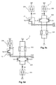
- FIG. 5a shows a differential stage 1 of a magnetic operational amplifier MOP according to a first embodiment of the invention.
- the differential stage 1 comprises a first magnetic field effect transistor MAGFET 11 and a differential signal conditioner.
- the first MAGFET 11 has a source S, a first drain D1 and a second drain D2, a gate voltage Vgate.
- the differential signal conditioner comprises:
- Figure 5b shows a differential stage 1 of a magnetic operational amplifier MOP according to a second embodiment of the invention, wherein the first magnetic field effect transistor MAGFET 11 is n-type magnetic field effect transistor MAGFET and the differential input pair 153 is a p-type differential input pair.
- Figure 5c shows a differential stage 1 of a magnetic operational amplifier MOP according to a third embodiment of the invention, wherein the first magnetic field effect transistor MAGFET 11 is a p-type magnetic field effect transistor and the differential input pair 153 is a p-type differential input pair.
- Figure 5d shows a differential stage 1 of a magnetic operational amplifier MOP according to a fourth embodiment of the invention, wherein the first magnetic field effect transistor MAGFET 11 is p-type magnetic field effect transistor and the differential input pair 153 is an n-type differential input pair.
- the differential stage 1 of the magnetic operational amplifier MOP may be associated to at least one amplification stage Amp1.
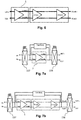
- Figure 6 shows the differential stage 1 of a magnetic operational amplifier MOP according to an embodiment of the invention, associated to N differential amplification stages Amp1, ..., AmpN with N a natural number greater than or equal to 2.
- Figure 7a shows the differential stage 1 of a magnetic operational amplifier MOP according to an embodiment of the invention, wherein the differential signal conditioner further comprises a chopper comprising a first stage 157 of modulation of a useful signal and a second stage 158 of demodulation of the useful signal.
- Figure 7b shows the differential stage 1 of a magnetic operational amplifier MOP according to an embodiment of the invention, associated to at least one amplification stage Amp1, and wherein the differential signal conditioner comprises the chopper having the first stage 157 of modulation of a useful signal and the second stage 158 of demodulation of the useful signal.
- Figure 8 shows a magnetic sensor 20 based on the use of four MOS transistors arranged in two parallel pairs crossing each other in order to form a pattern inscribed in a square.
- the magnetic sensor 20 comprises a square gate G that is common to all transistors. At each angle of the square gate G, two perpendicular contacts of the original transistors are connected so as to form a so called "angle-contact".
- the magnetic sensor 20 thus comprises four angle-contacts positioned at each angle of the square gate G: a first angle-contact A, a second angle-contact B, a third angle-contact C and a fourth angle-contact D.
- the structure of such a magnetic sensor is for example further described in the article " A Novel Chopping-Spinning MAGFET Device", by V. Frick et al. (2010 ).
- Figure 9a illustrates a first configuration of the magnetic sensor 20, wherein the third angle-contact C and the fourth angle-contact D are connected together to form a source, the first angle-contact A is a first drain and the second angle-contact B is a second drain.
- the magnetic sensor 20 in its first configuration is the first MAGFET 11.
- a source current I S is used to bias the magnetic sensor 20 forming the first MAGFET 11.
- a first drain current I D1 circulates in the first drain A and a second drain current I D2 circulates in the second drain B of the magnetic sensor 20 forming the first MAGFET 11.
- Figure 9b illustrates a second configuration of the magnetic sensor 20, wherein the first angle-contact A and the fourth angle-contact D are connected together to form a source, the second angle-contact B is a first drain and the third angle-contact C is a second drain.
- the magnetic sensor 20 in its second configuration is a second MAGFET 12.
- a source current I S is used to bias the magnetic sensor 20 forming the second MAGFET 12.
- a first drain current I D1 circulates in the first drain B and a second drain current I D2 circulates in the second drain C of the magnetic sensor 20 forming the second MAGFET 12.
- Figure 9c illustrates a third configuration of the magnetic sensor 20, wherein the second angle-contact B and the third angle-contact C are connected together to form a source, the fourth angle-contact D is a first drain and the first angle-contact A is a second drain.
- the magnetic sensor 20 in its third configuration is a third MAGFET 13.
- a source current I S is used to bias the magnetic sensor 20 forming the third MAGFET 13.
- a first drain current I D1 circulates in the first drain D and a second drain current I D2 circulates in the second drain A of the magnetic sensor 20 forming the third MAGFET 13.
- Figure 9d illustrates a fourth configuration of the magnetic sensor 20, wherein the first angle-contact A and the second angle-contact B are connected together to form a source, the third angle-contact C is a first drain and the fourth angle-contact D is a second drain.
- the magnetic sensor 20 in its fourth configuration is a fourth MAGFET 14.
- a source current I S is used to bias the magnetic sensor 20 forming the fourth MAGFET 14.
- a first drain current I D1 circulates in the first drain C and a second drain current I D2 circulates in the second drain D of the magnetic sensor 20 forming the fourth MAGFET 14.
- the magnetic sensor 20 comprising four MAGFET configurations is preferentially used in a magnetic operational amplifier according to an embodiment of the invention, instead of a single classical MAGFET.
- the symmetrical shape of the magnetic sensor 20 allows applying a spinning-current technique in order to remove the offset and low-frequency noise of the magnetic sensor 20.
- Figure 10 shows the differential stage 1 of a magnetic amplifier MOP comprising the magnetic sensor 20, wherein the differential signal conditioner further comprises a spinning-current module 159 that periodically alternates the first, second, third and fourth configurations of the magnetic sensor 20.
- Figure 10 shows a particular embodiment where each MAGFET configuration of the magnetic sensor 20 is an n-type MAGFET configuration and the differential input pair 153 is an n-type differential input pair; connections are thus similar to those of figure 5a .
- Other embodiments, not shown, are possible, where:
Landscapes
- Engineering & Computer Science (AREA)
- Power Engineering (AREA)
- Physics & Mathematics (AREA)
- Condensed Matter Physics & Semiconductors (AREA)
- General Physics & Mathematics (AREA)
- Amplifiers (AREA)
- Measuring Magnetic Variables (AREA)
Abstract
According to an aspect of the invention, it is provided a magnetic operational amplifier having a differential stage (1) comprising a first magnetic field effect transistor MAGFET (11) and a differential signal conditioner, the differential signal conditioner comprising a charge stage (151), a differential input pair (153) connected to the charge stage (151) and a biasing current source (155) connected to the differential input pair (153); the magnetic field effect transistor MAGFET (11) being connected to the charge stage (151) as a second differential input pair and the differential signal conditioner comprising a second biasing current source (156) connected to the magnetic field effect transistor MAGFET (11).
Description
- An aspect of the present invention relates to the technical field of magnetic field effect transistors MAGFET, and in particular to the technical field of magnetic operational amplifiers.
-
Figure 1 illustrates the structure of a classical differential amplifier stage A1 that comprises: - a
charge stage 151, - a
differential input pair 153 having a terminal Vin- and a terminal Vin+, - and a biasing
current source 155. - A biasing current source injects and maintains a constant current in a branch of an electric circuit. In the example of
figure 1 , the constant current injected and maintained by the biasingcurrent source 155 is named Ipol. The biasing current Ipol is maintained constant regardless of the variations applied to the currents IN and IP circulating in thedifferential input pair 153 and the following equation applies:
- Thanks to the
differential input pair 153, the difference between the currents IN and IP is proportional to the difference between the potentials applied to the terminal Vin- and to the terminal Vin+. - Thanks to the
charge stage 151, the difference between the currents IN and IP is converted into a voltage, thus giving an amplified image of the potential difference applied to the terminals Vin- and Vin+. - Three configurations of the differential stage of a magnetic operational amplifier MOP using a magnetic field effect transistor MAGFET are known.
-
Figure 2 illustrates a first differential stage A2 of a MOP comprising: - the
charge stage 151, - the
differential input pair 153 with terminals Vin- and Vin+, and - a
MAGFET 255 used in a current mirror. - Used in a current mirror as a biasing current source, the MAGFET 255 has to insure a total biasing current in the
differential input pair 153 that allows biasing-current proportional open-loop gain of the MOP. Said constraint prevents from controlling the gate voltage of theMAGFET 255. Said constraint thus prevents from choosing the operating regime of theMAGFET 255 and affects its performances, in particular in terms of sensitivity, thermal noise, consumption. -
Figure 3 illustrates a second differential stage A3 of a MOP comprising: - a MAGFET 351 as a charge stage,
- the
differential input pair 153 with terminals Vin- and Vin+, and - the biasing
current source 155. - Used as a charge stage and in order to insure the stability of the common mode at the output of the MOP, the gate of the
MAGFET 351 has to be controlled by the application of a constant voltage or by a control amplifier of the common mode used in a negative feedback. Controlling the gate of theMAGFET 351 by the application of a constant voltage prevents from choosing the operating regime of theMAGFET 255. When controlling the gate of theMAGFET 351 by a negative feedback of a control amplifier of the common mode, a variation of the gate voltage implies a variation in sensitivity for the MOP. In other words, the sensitivity of the MOP varies according to the control voltage of the common mode: the sensing function of the MOP A3 is therefore unusable. - Finally, two MAGFET may be used as a differential input pair, allowing to apply an external voltage and thus to realize a function, such as an amplifier or a follower for example.
Figure 4 illustrates a third differential stage A4 of a MOP comprising: - the
charge stage 151, - a first MAGFET 453 and a
second MAGFET 454 as a differential input pair with terminals Vin- and Vin+, and - the biasing
current source 155. - But applying an external voltage on the gate of a MAGFET implies a variation of its sensitivity: the same problem arises, as for the MAGFET used as charge stage.
- An objective of the invention is to realize a magnetic operational amplifier MOP based on a magnetic field effect transistor MAGFET whose operating regime may be freely chosen.
- To this end, according to an aspect of the invention, it is provided a magnetic operational amplifier having a differential stage comprising:
- a first magnetic field effect transistor MAGFET and
- a differential signal conditioner comprising:
- o a charge stage,
- o a differential input pair connected to the charge stage and
- o a biasing current source connected to the differential input pair,
- Thanks to the invention, the gate voltage and the biasing current of the magnetic field effect transistor MAGFET are independent of the biasing current of the differential input pair. The operating regime of the magnetic field effect transistor MAGFET is thus totally controllable.
- Apart from the characteristics mentioned above in the previous paragraph, the magnetic operational amplifier according to an aspect of the invention may have one or several complementary characteristics among the following characteristics considered individually or in any technically possible combinations:
- The first magnetic field effect transistor MAGFET is preferentially an n-type magnetic field effect transistor MAGFET, because an n-type magnetic field effect transistor MAGFET typically has a better mobility and thus a better sensitivity to a magnetic field than a p-type magnetic field effect transistor MAGFET. The first magnetic field effect transistor MAGFET may alternatively be a p-type magnetic field effect transistor MAGFET.
- The differential input pair can equally bean n-type or p-type differential input pair.
- The differential signal conditioner comprises at least one differential amplification stage to further amplify a useful signal.
- The differential signal conditioner further comprises a chopper to eliminate the offset and low-frequency noise of the differential signal conditioner, the chopper comprising a first stage of modulation of a useful signal and a second stage of demodulation of the useful signal, the useful signal entering the second stage of demodulation being a voltage.
- When the differential signal conditioner comprises at least one differential amplification stage and a chopper, the second stage of demodulation of the chopper is placed after the last differential amplification stage to eliminate the offset and low-frequency noise of the differential signal conditioner and of each differential amplification stage.
- The magnetic operational amplifier comprises a magnetic sensor connected to the charge stage as a second differential input pair and having:
- o a first configuration corresponding to the first magnetic field effect transistor MAGFET,
- o a second configuration corresponding to a second magnetic field effect transistor MAGFET,
- o a third configuration corresponding to a third magnetic field effect transistor MAGFET and
- o a fourth configuration corresponding to a fourth magnetic field effect transistor MAGFET,
-
- -
Figure 1 illustrates the structure of a classical differential amplifier stage. - -
Figure 2 illustrates a first differential stage of a magnetic operational amplifier MOP based on a magnetic field effect transistor MAGFET, according to the previous art. - -
Figure 3 illustrates a second differential stage of a magnetic operational amplifier MOP based on a magnetic field effect transistor MAGFET, according to the previous art. - -
Figure 4 illustrates a third differential stage of a magnetic operational amplifier MOP based on a magnetic field effect transistor MAGFET, according to the previous art. - -
Figure 5a illustrates a differential stage of a magnetic operational amplifier MOP based on a first magnetic field effect transistor MAGFET, according to a first embodiment of the invention. - -
Figure 5b illustrates a differential stage of a magnetic operational amplifier MOP based on a first magnetic field effect transistor MAGFET, according to a second embodiment of the invention. - -
Figure 5c illustrates a differential stage of a magnetic operational amplifier MOP based on a first magnetic field effect transistor MAGFET, according to a third embodiment of the invention. - -
Figure 5d illustrates a differential stage of a magnetic operational amplifier MOP based on a first magnetic field effect transistor MAGFET, according to a fourth embodiment of the invention. - -
Figure 6 illustrates the differential stage of a magnetic operational amplifier MOP based on a first magnetic field effect transistor MAGFET according to an embodiment of the invention, associated to differential amplification stages. - -
Figure 7a illustrates the differential stage of a magnetic operational amplifier MOP based on a first magnetic field effect transistor MAGFET according to an embodiment of the invention, associated to a chopper. - -
Figure 7b illustrates the differential stage of a magnetic operational amplifier MOP based on a first magnetic field effect transistor MAGFET according to an embodiment of the invention, associated to differential amplification stages and to a chopper. - -
Figure 8 illustrates a magnetic sensor having four possible symmetric MAGFET configurations. - -
Figure 9a illustrates a first configuration of the magnetic sensor offigure 8 , corresponding to the first magnetic field effect transistor MAGFET offigures 5a, 5b ,5c and 5d . - -
Figure 9b illustrates a second configuration of the magnetic sensor offigure 8 , corresponding to a second magnetic field effect transistor MAGFET. - -
Figure 9c illustrates a third configuration of the magnetic sensor offigure 8 , corresponding to a third magnetic field effect transistor MAGFET. - -
Figure 9d illustrates a fourth configuration of the magnetic sensor offigure 8 , corresponding to a fourth magnetic field effect transistor MAGFET. - -
Figure 10 illustrates the differential stage of a magnetic operational amplifier MOP based on the magnetic sensor offigure 8 having four possible symmetric MAGFET configurations, associated to a spinning current module. - Some embodiments of apparatus and methods in accordance with embodiments of the present invention are now described, by way of example only, and with reference to the accompanying drawings. The description is to be regarded as illustrative in nature and not as restricted.
-
Figure 1, figure 2, figure 3 and figure 4 have been previously described. -
Figure 5a shows adifferential stage 1 of a magnetic operational amplifier MOP according to a first embodiment of the invention. Thedifferential stage 1 comprises a first magnetic fieldeffect transistor MAGFET 11 and a differential signal conditioner. Thefirst MAGFET 11 has a source S, a first drain D1 and a second drain D2, a gate voltage Vgate. The differential signal conditioner comprises: - a
charge stage 151, - a
differential input pair 153 connected to thecharge stage 151, - a biasing
current source 155 connected to thedifferential input pair 153 and - a second biasing
current source 156 connected to thefirst MAGFET 11. -
Figure 5b shows adifferential stage 1 of a magnetic operational amplifier MOP according to a second embodiment of the invention, wherein the first magnetic fieldeffect transistor MAGFET 11 is n-type magnetic field effect transistor MAGFET and thedifferential input pair 153 is a p-type differential input pair. -
Figure 5c shows adifferential stage 1 of a magnetic operational amplifier MOP according to a third embodiment of the invention, wherein the first magnetic fieldeffect transistor MAGFET 11 is a p-type magnetic field effect transistor and thedifferential input pair 153 is a p-type differential input pair. -
Figure 5d shows adifferential stage 1 of a magnetic operational amplifier MOP according to a fourth embodiment of the invention, wherein the first magnetic fieldeffect transistor MAGFET 11 is p-type magnetic field effect transistor and thedifferential input pair 153 is an n-type differential input pair. - The
differential stage 1 of the magnetic operational amplifier MOP may be associated to at least one amplification stage Amp1.Figure 6 shows thedifferential stage 1 of a magnetic operational amplifier MOP according to an embodiment of the invention, associated to N differential amplification stages Amp1, ..., AmpN with N a natural number greater than or equal to 2. -
Figure 7a shows thedifferential stage 1 of a magnetic operational amplifier MOP according to an embodiment of the invention, wherein the differential signal conditioner further comprises a chopper comprising afirst stage 157 of modulation of a useful signal and asecond stage 158 of demodulation of the useful signal. -
Figure 7b shows thedifferential stage 1 of a magnetic operational amplifier MOP according to an embodiment of the invention, associated to at least one amplification stage Amp1, and wherein the differential signal conditioner comprises the chopper having thefirst stage 157 of modulation of a useful signal and thesecond stage 158 of demodulation of the useful signal. -
Figure 8 shows amagnetic sensor 20 based on the use of four MOS transistors arranged in two parallel pairs crossing each other in order to form a pattern inscribed in a square. Themagnetic sensor 20 comprises a square gate G that is common to all transistors. At each angle of the square gate G, two perpendicular contacts of the original transistors are connected so as to form a so called "angle-contact". Themagnetic sensor 20 thus comprises four angle-contacts positioned at each angle of the square gate G: a first angle-contact A, a second angle-contact B, a third angle-contact C and a fourth angle-contact D. The structure of such a magnetic sensor is for example further described in the article "A Novel Chopping-Spinning MAGFET Device", by V. Frick et al. (2010). - By electronically connecting two adjacent angle-contacts together to create a source and leaving the remaining two angle-contacts independent to create split drains, one creates a split-drain MAGFET structure where the source is twice the width of each drain. The symmetry of the
magnetic sensor 20 allows creating four identical MAGFET devices in four perpendicular directions. -
Figure 9a illustrates a first configuration of themagnetic sensor 20, wherein the third angle-contact C and the fourth angle-contact D are connected together to form a source, the first angle-contact A is a first drain and the second angle-contact B is a second drain. Themagnetic sensor 20 in its first configuration is thefirst MAGFET 11. A source current IS is used to bias themagnetic sensor 20 forming thefirst MAGFET 11. A first drain current ID1 circulates in the first drain A and a second drain current ID2 circulates in the second drain B of themagnetic sensor 20 forming thefirst MAGFET 11. -
Figure 9b illustrates a second configuration of themagnetic sensor 20, wherein the first angle-contact A and the fourth angle-contact D are connected together to form a source, the second angle-contact B is a first drain and the third angle-contact C is a second drain. Themagnetic sensor 20 in its second configuration is asecond MAGFET 12. A source current IS is used to bias themagnetic sensor 20 forming thesecond MAGFET 12. A first drain current ID1 circulates in the first drain B and a second drain current ID2 circulates in the second drain C of themagnetic sensor 20 forming thesecond MAGFET 12. -
Figure 9c illustrates a third configuration of themagnetic sensor 20, wherein the second angle-contact B and the third angle-contact C are connected together to form a source, the fourth angle-contact D is a first drain and the first angle-contact A is a second drain. Themagnetic sensor 20 in its third configuration is athird MAGFET 13. A source current IS is used to bias themagnetic sensor 20 forming thethird MAGFET 13. A first drain current ID1 circulates in the first drain D and a second drain current ID2 circulates in the second drain A of themagnetic sensor 20 forming thethird MAGFET 13. -
Figure 9d illustrates a fourth configuration of themagnetic sensor 20, wherein the first angle-contact A and the second angle-contact B are connected together to form a source, the third angle-contact C is a first drain and the fourth angle-contact D is a second drain. Themagnetic sensor 20 in its fourth configuration is afourth MAGFET 14. A source current IS is used to bias themagnetic sensor 20 forming thefourth MAGFET 14. A first drain current ID1 circulates in the first drain C and a second drain current ID2 circulates in the second drain D of themagnetic sensor 20 forming thefourth MAGFET 14. - The
magnetic sensor 20 comprising four MAGFET configurations is preferentially used in a magnetic operational amplifier according to an embodiment of the invention, instead of a single classical MAGFET. Indeed the symmetrical shape of themagnetic sensor 20 allows applying a spinning-current technique in order to remove the offset and low-frequency noise of themagnetic sensor 20.Figure 10 shows thedifferential stage 1 of a magnetic amplifier MOP comprising themagnetic sensor 20, wherein the differential signal conditioner further comprises a spinning-current module 159 that periodically alternates the first, second, third and fourth configurations of themagnetic sensor 20.Figure 10 shows a particular embodiment where each MAGFET configuration of themagnetic sensor 20 is an n-type MAGFET configuration and thedifferential input pair 153 is an n-type differential input pair; connections are thus similar to those offigure 5a . Other embodiments, not shown, are possible, where: - each MAGFET configuration of the
magnetic sensor 20 is an n-type MAGFET configuration and thedifferential input pair 153 is a p-type differential input pair; connections are then similar to those offigure 5b , or - each MAGFET configuration of the
magnetic sensor 20 is a p-type MAGFET configuration and thedifferential input pair 153 is a p-type differential input pair; connections are then similar to those offigure 5c , or - each MAGFET configuration of the
magnetic sensor 20 is a p-type MAGFET configuration and thedifferential input pair 153 is a n-type differential input pair; connections are then similar to those offigure 5d .
Claims (6)
- A magnetic operational amplifier having a differential stage (1) comprising:- a first magnetic field effect transistor MAGFET (11) and- a differential signal conditioner comprising:characterised in that the first magnetic field effect transistor MAGFET (11) is connected to the charge stage (151) as a second differential input pair and in that the differential signal conditioner comprises a second biasing current source (156) connected to the magnetic field effect transistor MAGFET (11).o a charge stage (151),o a differential input pair (153) connected to the charge stage (151) ando a biasing current source (155) connected to the differential input pair (153),
- The magnetic operational amplifier according to the preceding claim characterised in that the first magnetic field effect transistor MAGFET (11) is an n-type magnetic field effect transistor MAGFET.
- The magnetic operational amplifier according to one of the preceding claims characterised in that the differential signal conditioner comprises at least one differential amplification stage (Amp1, AmpN) to further amplify a useful signal.
- The magnetic operational amplifier according to one of the preceding claims characterised in that the differential signal conditioner further comprises a chopper to eliminate the offset and low-frequency noise of the differential signal conditioner, the chopper comprising a first stage (157) of modulation of a useful signal and a second stage (158) of demodulation of the useful signal, the useful signal entering the second stage (158) of demodulation being a voltage.
- The magnetic operational amplifier according to claims 3 and 4 characterised in that the second stage (158) of demodulation of the chopper is placed after the last differential amplification stage to eliminate the offset and low-frequency noise of the differential signal conditioner and of each differential amplification stage.
- The magnetic operational amplifier according to one of the preceding claims characterised in that it comprises a magnetic sensor (20) connected to the charge stage (151) as a second differential input pair and having:- a first configuration corresponding to the first magnetic field effect transistor MAGFET (11),- a second configuration corresponding to a second magnetic field effect transistor MAGFET (12),- a third configuration corresponding to a third magnetic field effect transistor MAGFET (13) and- a fourth configuration corresponding to a fourth magnetic field effect transistor MAGFET (14),and characterised in that the differential signal conditioner further comprises a spinning current module (159) to eliminate the offset and low-frequency noise of the magnetic sensor (20), the spinning current module (159) periodically alternating the first (11), second (12), third (13) and fourth (14) configurations of the magnetic sensor (20).
Priority Applications (5)
| Application Number | Priority Date | Filing Date | Title |
|---|---|---|---|
| EP16169019.3A EP3244532A1 (en) | 2016-05-10 | 2016-05-10 | Magnetic operational amplifier |
| PCT/EP2017/060245 WO2017194334A1 (en) | 2016-05-10 | 2017-04-28 | Magnetic operational amplifier |
| EP17720133.2A EP3455937A1 (en) | 2016-05-10 | 2017-04-28 | Magnetic operational amplifier |
| US16/099,902 US10879860B2 (en) | 2016-05-10 | 2017-04-28 | Magnetic operational amplifier |
| CN201780027374.4A CN109155613A (en) | 2016-05-10 | 2017-04-28 | magnetic operational amplifier |
Applications Claiming Priority (1)
| Application Number | Priority Date | Filing Date | Title |
|---|---|---|---|
| EP16169019.3A EP3244532A1 (en) | 2016-05-10 | 2016-05-10 | Magnetic operational amplifier |
Publications (1)
| Publication Number | Publication Date |
|---|---|
| EP3244532A1 true EP3244532A1 (en) | 2017-11-15 |
Family
ID=55963224
Family Applications (2)
| Application Number | Title | Priority Date | Filing Date |
|---|---|---|---|
| EP16169019.3A Withdrawn EP3244532A1 (en) | 2016-05-10 | 2016-05-10 | Magnetic operational amplifier |
| EP17720133.2A Withdrawn EP3455937A1 (en) | 2016-05-10 | 2017-04-28 | Magnetic operational amplifier |
Family Applications After (1)
| Application Number | Title | Priority Date | Filing Date |
|---|---|---|---|
| EP17720133.2A Withdrawn EP3455937A1 (en) | 2016-05-10 | 2017-04-28 | Magnetic operational amplifier |
Country Status (4)
| Country | Link |
|---|---|
| US (1) | US10879860B2 (en) |
| EP (2) | EP3244532A1 (en) |
| CN (1) | CN109155613A (en) |
| WO (1) | WO2017194334A1 (en) |
Families Citing this family (1)
| Publication number | Priority date | Publication date | Assignee | Title |
|---|---|---|---|---|
| CN108377137B (en) * | 2018-05-07 | 2024-06-04 | 贵州大学 | High-voltage high-power integrated operational amplifier |
Citations (3)
| Publication number | Priority date | Publication date | Assignee | Title |
|---|---|---|---|---|
| EP1830162A1 (en) * | 2004-12-14 | 2007-09-05 | Ntn Corporation | Rotation detecting apparatus and bearing provided with same |
| US20070268060A1 (en) * | 2006-05-19 | 2007-11-22 | National Semiconductor Germany Ag | Method and circuit arrangement for generating a periodic electric signal with controllable phase |
| EP2005582A1 (en) * | 2006-03-23 | 2008-12-24 | Nxp B.V. | Converter with parallel coupled differential input pairs |
Family Cites Families (13)
| Publication number | Priority date | Publication date | Assignee | Title |
|---|---|---|---|---|
| WO1994012238A1 (en) * | 1992-11-24 | 1994-06-09 | Medtronic, Inc. | Implantable medical device with magnetically actuated switch |
| US5801533A (en) * | 1996-09-17 | 1998-09-01 | Intel Corporation | Method and apparatus with cascode biasing magneto field effect transistors for improved sensitivity and amplification |
| US6469538B1 (en) * | 2000-06-09 | 2002-10-22 | Stmicroelectronics, Inc. | Current monitoring and latchup detection circuit and method of operation |
| US6831513B2 (en) * | 2002-01-16 | 2004-12-14 | Oki Electric Industry Co., Ltd. | Differential amplifier |
| US7199434B2 (en) * | 2003-12-05 | 2007-04-03 | Nanyang Technological University | Magnetic field effect transistor, latch and method |
| US7642851B2 (en) * | 2007-06-25 | 2010-01-05 | Metalink Ltd. | Variable gain amplifier insensitive to process voltage and temperature variations |
| US7733179B2 (en) * | 2007-10-31 | 2010-06-08 | Texas Instruments Incorporated | Combination trim and CMFB circuit and method for differential amplifiers |
| JPWO2011092769A1 (en) * | 2010-02-01 | 2013-05-30 | パナソニック株式会社 | Operational amplifier circuit, signal driving device, display device, and offset voltage adjusting method |
| US8482352B2 (en) * | 2010-06-30 | 2013-07-09 | International Business Machines Corporation | Differential amplifier stage with integrated offset cancellation circuit |
| CN103051298B (en) * | 2011-10-17 | 2016-07-06 | 中国科学院微电子研究所 | Programmable Gain Amplifier Circuit and programmable gain amplifier |
| JP2015095830A (en) * | 2013-11-13 | 2015-05-18 | 株式会社東芝 | Differential amplification circuit |
| US9915641B2 (en) * | 2013-12-04 | 2018-03-13 | California Institute Of Technology | Sensing and actuation of biological function using addressable transmitters operated as magnetic spins |
| US9312825B2 (en) * | 2014-05-09 | 2016-04-12 | Analog Devices Global | Amplifier input stage and amplifier |
-
2016
- 2016-05-10 EP EP16169019.3A patent/EP3244532A1/en not_active Withdrawn
-
2017
- 2017-04-28 CN CN201780027374.4A patent/CN109155613A/en active Pending
- 2017-04-28 EP EP17720133.2A patent/EP3455937A1/en not_active Withdrawn
- 2017-04-28 US US16/099,902 patent/US10879860B2/en not_active Expired - Fee Related
- 2017-04-28 WO PCT/EP2017/060245 patent/WO2017194334A1/en not_active Ceased
Patent Citations (3)
| Publication number | Priority date | Publication date | Assignee | Title |
|---|---|---|---|---|
| EP1830162A1 (en) * | 2004-12-14 | 2007-09-05 | Ntn Corporation | Rotation detecting apparatus and bearing provided with same |
| EP2005582A1 (en) * | 2006-03-23 | 2008-12-24 | Nxp B.V. | Converter with parallel coupled differential input pairs |
| US20070268060A1 (en) * | 2006-05-19 | 2007-11-22 | National Semiconductor Germany Ag | Method and circuit arrangement for generating a periodic electric signal with controllable phase |
Non-Patent Citations (5)
| Title |
|---|
| CHIEN-HUNG KUO ET AL: "CMOS Oversampling Magnetic-to-Digital Converters", IEEE JOURNAL OF SOLID-STATE CIRCUITS, IEEE SERVICE CENTER, PISCATAWAY, NJ, USA, vol. 36, no. 10, 1 October 2001 (2001-10-01), XP011061607, ISSN: 0018-9200 * |
| LEE-AN HO ET AL: "CMOS oversampling /spl Delta Sigma/ magnetic to digital converters", CONFERENCE PROCEEDINGS / ISCAS 2001, THE 2001 IEEE INTERNATIONAL SYMPOSIUM ON CIRCUITS AND SYSTEMS : 06 - 09 MAY 2001, SYDNEY CONVENTION AND EXHIBITION CENTRE, DARLING HARBOUR, SYDNEY, AUSTRALIA, IEEE SERVICE CENTER, PISCATAWAY, NJ, vol. 1, 6 May 2001 (2001-05-06), pages 388 - 391, XP010541448, ISBN: 978-0-7803-6685-5, DOI: 10.1109/ISCAS.2001.921874 * |
| LIU S ET AL: "SPICE MACRO MODEL FOR MAGFET AND ITS APPLICATIONS", IEEE TRANSACTIONS ON CIRCUITS AND SYSTEMS II: ANALOG AND DIGITALSIGNAL PROCESSING, INSTITUTE OF ELECTRICAL AND ELECTRONICS ENGINEERS INC, 345 EAST 47 STREET, NEW YORK, N.Y. 10017, USA, vol. 46, no. 4, 1 April 1999 (1999-04-01), pages 370 - 375, XP000902763, ISSN: 1057-7130, DOI: 10.1109/82.803472 * |
| V. FRICK ET AL., A NOVEL CHOPPING-SPINNING MAGFET DEVICE, 2010 |
| VINCENT FRICK ET AL: "A novel chopping-spinning MAGFET device", ELECTRONICS, CIRCUITS, AND SYSTEMS (ICECS), 2010 17TH IEEE INTERNATIONAL CONFERENCE ON, IEEE, 12 December 2010 (2010-12-12), pages 815 - 818, XP031923079, ISBN: 978-1-4244-8155-2, DOI: 10.1109/ICECS.2010.5724637 * |
Also Published As
| Publication number | Publication date |
|---|---|
| US10879860B2 (en) | 2020-12-29 |
| US20190181818A1 (en) | 2019-06-13 |
| CN109155613A (en) | 2019-01-04 |
| WO2017194334A1 (en) | 2017-11-16 |
| EP3455937A1 (en) | 2019-03-20 |
Similar Documents
| Publication | Publication Date | Title |
|---|---|---|
| JP2009159610A (en) | Current sampling method and circuit | |
| US9887689B2 (en) | Pseudo resistance circuit and charge detection circuit | |
| EP1435693B1 (en) | Amplification circuit | |
| EP3244532A1 (en) | Magnetic operational amplifier | |
| US20190081625A1 (en) | Device modifying the impedance value of a reference resistor | |
| US10224886B2 (en) | Operational amplifier circuit using variable bias control | |
| KR100574968B1 (en) | Operational Amplifier with Offset Compensation Circuit | |
| US20150263679A1 (en) | Inverting amplifier | |
| US9246455B2 (en) | Three stage amplifier | |
| US11095258B2 (en) | Class AB amplifier and operational amplifier | |
| US7629846B2 (en) | Source follower circuit and semiconductor apparatus | |
| US7714653B2 (en) | Differential amplifier | |
| US10404228B2 (en) | Transconductance amplifier and phase shifter | |
| US8416021B2 (en) | Amplifier circuit | |
| US20090261905A1 (en) | Open gain adjustment circuit for operational amplifier | |
| KR102089870B1 (en) | Hall sensor using current signal | |
| EP2216902B1 (en) | Bias circuit and method for controlling bias circuit | |
| US7646243B2 (en) | Controlled transconductance differential stage | |
| US20150015326A1 (en) | Bulk-modulated current source | |
| EP3187885B1 (en) | A current sensing circuit and method | |
| US9515624B2 (en) | Semiconductor device | |
| EP1655833A1 (en) | Class B amplifier with process variation independent deadband | |
| JP2015035761A (en) | Switched capacitor circuit | |
| JP2003273672A (en) | Differential amplifier circuit | |
| US9923522B2 (en) | Operational amplifier circuit and bias current supply method |
Legal Events
| Date | Code | Title | Description |
|---|---|---|---|
| PUAI | Public reference made under article 153(3) epc to a published international application that has entered the european phase |
Free format text: ORIGINAL CODE: 0009012 |
|
| AK | Designated contracting states |
Kind code of ref document: A1 Designated state(s): AL AT BE BG CH CY CZ DE DK EE ES FI FR GB GR HR HU IE IS IT LI LT LU LV MC MK MT NL NO PL PT RO RS SE SI SK SM TR |
|
| AX | Request for extension of the european patent |
Extension state: BA ME |
|
| STAA | Information on the status of an ep patent application or granted ep patent |
Free format text: STATUS: THE APPLICATION IS DEEMED TO BE WITHDRAWN |
|
| 18D | Application deemed to be withdrawn |
Effective date: 20180516 |