EP3244486A1 - Antenna device for the coexistence of wireless systems - Google Patents
Antenna device for the coexistence of wireless systems Download PDFInfo
- Publication number
- EP3244486A1 EP3244486A1 EP16305532.0A EP16305532A EP3244486A1 EP 3244486 A1 EP3244486 A1 EP 3244486A1 EP 16305532 A EP16305532 A EP 16305532A EP 3244486 A1 EP3244486 A1 EP 3244486A1
- Authority
- EP
- European Patent Office
- Prior art keywords
- antenna
- slot
- antennas
- conductive layer
- antenna device
- Prior art date
- Legal status (The legal status is an assumption and is not a legal conclusion. Google has not performed a legal analysis and makes no representation as to the accuracy of the status listed.)
- Withdrawn
Links
- 230000005540 biological transmission Effects 0.000 claims abstract description 7
- 230000001360 synchronised effect Effects 0.000 claims description 4
- PEZNEXFPRSOYPL-UHFFFAOYSA-N (bis(trifluoroacetoxy)iodo)benzene Chemical compound FC(F)(F)C(=O)OI(OC(=O)C(F)(F)F)C1=CC=CC=C1 PEZNEXFPRSOYPL-UHFFFAOYSA-N 0.000 description 8
- 238000002955 isolation Methods 0.000 description 6
- 238000004088 simulation Methods 0.000 description 4
- IYZWUWBAFUBNCH-UHFFFAOYSA-N 2,6-dichlorobiphenyl Chemical compound ClC1=CC=CC(Cl)=C1C1=CC=CC=C1 IYZWUWBAFUBNCH-UHFFFAOYSA-N 0.000 description 1
- 239000003990 capacitor Substances 0.000 description 1
- 230000015556 catabolic process Effects 0.000 description 1
- 230000008878 coupling Effects 0.000 description 1
- 238000010168 coupling process Methods 0.000 description 1
- 238000005859 coupling reaction Methods 0.000 description 1
- 238000006731 degradation reaction Methods 0.000 description 1
- 230000000694 effects Effects 0.000 description 1
- 238000005516 engineering process Methods 0.000 description 1
- 230000007613 environmental effect Effects 0.000 description 1
- 238000009413 insulation Methods 0.000 description 1
- 239000002184 metal Substances 0.000 description 1
- 229910052751 metal Inorganic materials 0.000 description 1
- 239000000758 substrate Substances 0.000 description 1
Images




Classifications
-
- H—ELECTRICITY
- H01—ELECTRIC ELEMENTS
- H01Q—ANTENNAS, i.e. RADIO AERIALS
- H01Q1/00—Details of, or arrangements associated with, antennas
- H01Q1/36—Structural form of radiating elements, e.g. cone, spiral, umbrella; Particular materials used therewith
- H01Q1/38—Structural form of radiating elements, e.g. cone, spiral, umbrella; Particular materials used therewith formed by a conductive layer on an insulating support
-
- H—ELECTRICITY
- H01—ELECTRIC ELEMENTS
- H01Q—ANTENNAS, i.e. RADIO AERIALS
- H01Q1/00—Details of, or arrangements associated with, antennas
- H01Q1/48—Earthing means; Earth screens; Counterpoises
-
- H—ELECTRICITY
- H01—ELECTRIC ELEMENTS
- H01Q—ANTENNAS, i.e. RADIO AERIALS
- H01Q1/00—Details of, or arrangements associated with, antennas
- H01Q1/52—Means for reducing coupling between antennas; Means for reducing coupling between an antenna and another structure
- H01Q1/521—Means for reducing coupling between antennas; Means for reducing coupling between an antenna and another structure reducing the coupling between adjacent antennas
-
- H—ELECTRICITY
- H01—ELECTRIC ELEMENTS
- H01Q—ANTENNAS, i.e. RADIO AERIALS
- H01Q13/00—Waveguide horns or mouths; Slot antennas; Leaky-waveguide antennas; Equivalent structures causing radiation along the transmission path of a guided wave
- H01Q13/10—Resonant slot antennas
-
- H—ELECTRICITY
- H01—ELECTRIC ELEMENTS
- H01Q—ANTENNAS, i.e. RADIO AERIALS
- H01Q21/00—Antenna arrays or systems
- H01Q21/28—Combinations of substantially independent non-interacting antenna units or systems
Definitions
- the present invention relates generally to the field of antennas for wireless systems. Particularly but not exclusively, embodiments of the invention relate to antenna devices comprising at least two antennas printed on a printed circuit board and arranged to operate on a time sharing transmission model, one of the antennas being a slot-type antenna.
- multimedia devices now comprise one or more antennas for exchanging data signals with other multimedia devices. These devices may comprise one or several antennas for transmitting and/or receiving data signals according to different communication standards.
- the multimedia device may for example comprise one or more antenna(s) for Wi-Fi communication and an antenna for Bluetooth (also referred to as BT) communication.
- Embodiments of the present invention will be introduced for a system comprising two MIMO antennas for Wi-Fi transmissions and one antenna for BT transmissions but it will be appreciated that the invention is not limited to such a system.
- Fig.1 represents a basic architecture of a printed circuit board (or PCB) 10 used for implementing such a system.
- the PCB 10 comprises two antennas, 11 and 12, for Wi-Fi communication and one antenna 13 for BT communication. These antennas are connected to respective radio chains.
- Wi-Fi and BT operate in the same frequency band, between 2.4 and 2.5GHz, interference issues arise when they operate simultaneously. There are two ways to manage these interference issues:
- Embodiments of the present invention concern devices wherein the second way is applied.
- Dedicated algorithms are used to control the radios according to a time sharing transmission model.
- embodiments of the present invention concerns antenna devices comprising at least two antennas operating in a same frequency band or close frequency bands, one of the two antennas being a slot-type antenna.
- the presence of the slot of the slot-type antenna has a negative impact on the efficiency of the other antennas of the device when they are in operation.
- the efficiency of the other antennas is reduced by a few percent (10% in the case of the antenna device of Figs.1 to 5 ).
- Embodiments of the present invention set out to to alleviate at least partially this drawback.
- a first aspect of the invention relates to an antenna device comprising a printed circuit board and at least first and second antennas printed on said printed circuit board, the printed circuit board comprising at least one conductive layer, wherein said first and second antennas are arranged to operate on a time sharing transmission model, and wherein the second antenna comprises a slot etched in said conductive layer, said slot having an open end at an edge of said conductive layer.
- the antenna device comprises a shunt circuit for shunting the open end of the slot of the second antenna when the first antenna is in operation.
- the slot-type antenna disrupt the flow of ground currents in the conductive layer of the printed circuit board when the first antenna is in operation.
- the open end of the slot is shunted when the first antenna is in operation in order to reduce the impact of the slot on the ground currents in the conductive layer of PCB when the first antenna is in operation. Consequently, the efficiency of the first antenna is improved.
- the shunt circuit comprises a PIN diode.
- the PIN diode is biased when the first antenna is in operation.
- the antenna device comprises a bias circuit for biasing the PIN diode, said bias circuit being synchronized on the operation of the first antenna.
- the first and second antennas operate in a same frequency band, for example the frequency band [2.4-2.5 GHz].
- Embodiments of the invention will be described by comparing the simulation results of the antenna system of Fig.1 (prior art) with the simulation results of a same antenna system equipped with a shunt circuit for shunting the open end of the slot-type antenna (embodiment of the invention).
- Figs.1 to 7 refer to an antenna system not equipped with a shunt circuit as proposed by embodiments of the present invention while Figs.8 to 10 refer to a same system antenna equipped with a shunt circuit as proposed by an embodiment of the present invention.
- the antenna system comprises a printed circuit board 10 and three antennas 11 to 13 printed on the printed circuit board.
- the printed circuit board 10 comprises a multi-layered substrate comprising three conductive layers separated from each other by dielectric layers.
- the antennas 11 and 12 are two identical dual-band MIMO antennas for Wi-Fi communications. These antennas are described in detail in the patent application EP2790268A1 .
- each of these antennas comprises two cascaded PIFAs (Printed Inverted-F Antenna) each resonating in a specific portion of the Wi-Fi bands.
- the dual-band antenna 11 comprises a first PIFA 21 on a first conductive layer and a second PIFA 22 on a second conductive layer.
- the ground planes are on both conductive layers.
- the PIFAs are cascaded in order to achieve a compact antenna.
- the first PIFA 21 comprises a first radiating element 210, a first feed element 211 connected to the first radiating element and a first ground return element 212
- the second PIFA 22 comprises a second radiating element 220, a second feed element 221 connected to the second radiating element and a second ground return element 222. Both ground return elements 212 222 are connected to the ground planes of all layers.
- Impedance matching components 23 are also provided at the common feeding port of the antenna.
- the operation and the detailed structure of such an antenna are described in detail in the patent application EP2790268A1 as mentioned before.
- other Wi-Fi antenna structures could be used for presenting embodiments of the invention.
- the antenna 13 which is the BT antenna, is a compact slot antenna which described in detail in the patent application EP2725658A1 .
- This antenna is briefly described hereinafter by referring to Figs.3 to 5 .
- M1, M2 and M3 designate the three superimposed conductive layers of the printed circuit board. These conductive layers are separated by dielectric layers D1 and D2. These layers are visible on Fig.4 .
- the antenna 13 is formed by a slot-line 30 etched in the intermediate conductive layer M2 and excited at the feeding point F by electromagnetic coupling with a feeding line 34 realised in micro-strip technology, either on the upper face of the dielectric layer D1 or on the lower face of the dielectric layer D2.
- the slot-line 30 continues by a slot-line 31 realised in the upper conductive layer M1 then by a slot-line 32 realised in the lower conductive layer M3, the slot-lines 30, 31, 32 being superimposed and their total electrical length being equal to k* ⁇ g where ⁇ g is the wavelength at the operating frequency.
- the feeding line 34 is connected to an impedance matching circuit 35.
- the slot-line 31 realised in the conductive layer M1 is delimited by two conductive strips S31 and S'31.
- the slot-line 32 is delimited by two conductive strips S32, S'32 in the conductive layer M3.
- the different conductive strips are interconnected in the following manner.
- the intermediate conductive layer M2 has, on each side of the slot-line 30, at the feeding side, two apertures W, W' through which pass two via-holes V1, V1' respectively connecting one of the ends of the conductive strip S31 to the corresponding end of the conductive strip S32 and one of the ends of the conductive strip S'31 with the corresponding end of the conductive strip S'32.
- the other end of the conductive strip S31 is connected through a via-hole V2 to the conductive layer M2 and to an isolated element EM of the conductive layer M3 located in the continuation of the conductive strip S32.
- the end of the conductive strip S'31 is connected to the intermediate layer M2 and to an isolated element EM' of the conductive layer M3 located in the continuation of the conductive strip S'32.
- This enables a connection to be obtained between the different slot-lines 30, 31, 32 as shown by the arrows in FIG.4 .
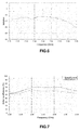
- These antennas have been 3D electromagnetically simulated with predefined mechanical and environmental constraints. The simulation results are illustrated by graphs of Fig.6 and Fig.7 .
- Fig.6 shows the isolation between the antenna 12 (Wi-Fi antenna) and the antenna 13 (BT antenna). As can be seen in this figure, the isolation level is around 11dB in the 2.4-2.5 GHz band. This level is low.
- Fig.7 shows two curves illustrating the efficiency of the antenna 12 in the presence and in the absence of the slot-type antenna 13. This Figure shows that, in presence of the slot-type antenna, the efficiency of the antenna 12 is reduced by around 10-12%, from around 70% to less than 60%, which is critical.
- the antenna device with a shunt circuit for shunting the open end of the slot of the slot-type antenna when the other antenna(s) of the antenna system is in operation in order to preserve the intrinsic performances of this or these other antenna(s).
- a shunt circuit 35 is provided between both sides of the open end of the slot of the antenna 13.
- shunt circuit 35 is shown schematically on Fig.8 . It comprises a PIN diode 350 and a bias circuit 351 for biasing the PIN diode, the whole circuit being placed between two connexion points P1 and P2 connected to both sides of the open end of the slot of the slot-type antenna.
- the bias circuit 351 comprises two capacitors C1 and C2 and an inductor L1 arranged to bias the diode 350 and control its state (conducting or not conducting) as a function of a control voltage Vb.
- Such a bias circuit is well known in the art.
- the role of the shunt circuit 35 is to neutralize the effect of the slot on the surrounding antennas of the antenna device when the latter are in operation.
- the shunting of the open end of the slot of the antenna 13 has been simulated by providing the open end of the slot of the antenna 13 with a short circuit SC acting as a shunt circuit as shown in Fig.9 .
- a metal strip forming the short circuit SC is placed at the open end of the slot.
- Fig.10 shows two curves illustrating the efficiency of the antenna 12 in the presence and in the absence of the slot-type antenna 13 equipped with the shunt circuit 35.
- the efficiency of the antenna 12 is recovered when the slot of the antenna 13 is shunted.
- This example shows that the efficiency degradation of the antenna 12 can be at least partially avoided by equipping the slot-type antenna 13 with a shunt circuit as disclosed hereinabove.
- the shunt circuit is advantageously a PIN diode and the bias circuit of the PIN diode is synchronized on the operation of the antenna 12. More specifically, the biasing of the PIN diode is synchronized with the operation of the antenna 12 such that:
- the antenna device comprises one slot-type antenna (antenna 13) and two PIFA antennas (antennas 11 and 12).
- the antenna device could comprise only one slot-type antenna and one PIFA antenna.
- the antenna(s) 11 and/or 12 are antennas designed on a PCB and not necessarily PIFA antennas.
- the slot-type antenna (antenna 13) and the PIFA antennas (antennas 11 and 12) operates in a same frequency band.
- Embodiments of the invention could be applied to antennas operating in close frequency bands.
Landscapes
- Waveguide Aerials (AREA)
- Details Of Aerials (AREA)
- Support Of Aerials (AREA)
Abstract
Embodiments of the present invention concern an antenna device comprising a printed circuit board and at least first and second antennas printed on said printed circuit board, said printed circuit board comprising at least one conductive layer. The first and second antennas are arranged to operate on a time sharing transmission model, and the second antenna comprises a slot (30,31,32) etched in said conductive layer, said slot having an open end at an edge of said conductive layer. According to an embodiment of the invention, the antenna device further comprises a shunt circuit for shunting the open end of the slot of the second antenna when the first antenna is in operation.
Description
- The present invention relates generally to the field of antennas for wireless systems. Particularly but not exclusively, embodiments of the invention relate to antenna devices comprising at least two antennas printed on a printed circuit board and arranged to operate on a time sharing transmission model, one of the antennas being a slot-type antenna.
- Many multimedia devices now comprise one or more antennas for exchanging data signals with other multimedia devices. These devices may comprise one or several antennas for transmitting and/or receiving data signals according to different communication standards. The multimedia device may for example comprise one or more antenna(s) for Wi-Fi communication and an antenna for Bluetooth (also referred to as BT) communication.
- Embodiments of the present invention will be introduced for a system comprising two MIMO antennas for Wi-Fi transmissions and one antenna for BT transmissions but it will be appreciated that the invention is not limited to such a system.
- Bluetooth (BT) and Wi-Fi complying with the standard IEEE-802.11 b/g/n operate in the same frequency band, between 2.4 and 2.5GHz, leading consequently to coexistence issues.
Fig.1 represents a basic architecture of a printed circuit board (or PCB) 10 used for implementing such a system. ThePCB 10 comprises two antennas, 11 and 12, for Wi-Fi communication and oneantenna 13 for BT communication. These antennas are connected to respective radio chains. - Since Wi-Fi and BT operate in the same frequency band, between 2.4 and 2.5GHz, interference issues arise when they operate simultaneously. There are two ways to manage these interference issues:
- 1) the first way, which is the most common one, is to ensure high insulation between the Wi-Fi and the Bluetooth antennas. To achieve this there are two solutions:
- 1.a) physically separating the antennas, for instance by a distance of more than half wavelength; this distance may be greater than 6 cm for a 2.4GHz wireless systems; this solution enables both radios to run "freely" without each performance being degraded by the concurrent radio; it allows also each Wi-Fi and BT antenna radiating omni-directionally without having to share the spatial radiating coverage; however this solution supposes that there is enough room to dispose the antennas in the device, which is rarely the case;
- 1.b) adding an isolation slot between the Wi-Fi and BT antennas or using other decoupling solutions; with this solution, the distance between antennas can be greatly reduced (lower than a quarter-wavelength) while achieving the required isolation; however the main drawback is that each antenna radiates selectively in a given direction without overlapping, thus not enabling them to radiate omni-directionally; consequently, this solution affects both Wi-Fi and BT radio performances in terms of spatial coverage; in addition, this solution still needs to have enough room to insert the isolation slot;
- 2/ the second way involves using an algorithm to manage the coexistence of both radios, enabling only one radio to run at the same time, sharing thus timely the wireless communication; as can be understood, with this way to manage the coexistence of the two systems, the Wi-Fi performances will depend strongly on the use case of the BT radio or inversely; if Wi-Fi is used for a video streaming application and BT is used for a remote control application, the impact for Wi-Fi will be huge and low for BT.
- Embodiments of the present invention concern devices wherein the second way is applied. Dedicated algorithms are used to control the radios according to a time sharing transmission model.
- More specifically, embodiments of the present invention concerns antenna devices comprising at least two antennas operating in a same frequency band or close frequency bands, one of the two antennas being a slot-type antenna.
- As will be described later in the present application in reference to
Figs.1 to 7 , the presence of the slot of the slot-type antenna has a negative impact on the efficiency of the other antennas of the device when they are in operation. The efficiency of the other antennas is reduced by a few percent (10% in the case of the antenna device ofFigs.1 to 5 ). - Embodiments of the present invention set out to to alleviate at least partially this drawback.
- A first aspect of the invention relates to an antenna device comprising a printed circuit board and at least first and second antennas printed on said printed circuit board, the printed circuit board comprising at least one conductive layer, wherein said first and second antennas are arranged to operate on a time sharing transmission model, and wherein the second antenna comprises a slot etched in said conductive layer, said slot having an open end at an edge of said conductive layer. According to an embodiment of the invention, the antenna device comprises a shunt circuit for shunting the open end of the slot of the second antenna when the first antenna is in operation.
- Indeed, simulations have demonstrated that the slot-type antenna disrupt the flow of ground currents in the conductive layer of the printed circuit board when the first antenna is in operation. In an embodiment of the invention, the open end of the slot is shunted when the first antenna is in operation in order to reduce the impact of the slot on the ground currents in the conductive layer of PCB when the first antenna is in operation. Consequently, the efficiency of the first antenna is improved.
- In a particular embodiment, the shunt circuit comprises a PIN diode.
- In a particular embodiment, the PIN diode is biased when the first antenna is in operation.
- In a particular embodiment, the antenna device comprises a bias circuit for biasing the PIN diode, said bias circuit being synchronized on the operation of the first antenna.
- In a particular embodiment, the first and second antennas operate in a same frequency band, for example the frequency band [2.4-2.5 GHz].
- The invention can be better understood with reference to the following description and drawings, given by way of example and not limiting the scope of protection, and in which:
-
Fig.1 is a schematic view of an antenna device comprising two Wi-Fi antennas and one Bluetooth antenna designed on a printed circuit board, the Bluetooth being a slot-type antenna; -
Fig.2 is an enlarged schematic view of one Wi-Fi antenna of the antenna device of Fig.l; -
Fig.3 is an enlarged schematic view of the Bluetooth antenna of the antenna device of Fig.l; -
Fig.4 is a schematic view showing the slot of the Wi-Fi antenna through the different conductive layers of the printed circuit board; -
Fig.5 is a perspective view of the Bluetooth antenna ofFig.3 ; -
Fig.6 is a graph illustrating the isolation between the Wi-Fi antenna 12 and the Bluetoothantenna 13 of antenna device of Fig.l; -
Fig.7 is a graph illustrating the efficiency of the Wi-Fi antenna 12 ofFig.1 with and without the presence of the Bluetoothantenna 13; -
Fig.8 is a schematic view of a shunting circuit in accordance with an embodiment of the invention; -
Fig.9 is a view identical to the view ofFig.5 wherein a short circuit is placed at the open end of the slot of the Bluetoothantenna 13; and -
Fig.10 is a graph illustrating the efficiency of the Wi-Fi antenna 12 ofFig.1 when theBT antenna 13 is equipped with a short circuit as illustrated byFig.9 . - The components in the figures are not necessarily to scale, emphasis instead being placed upon illustrating the principles of the invention.
- Embodiments of the invention will be described by comparing the simulation results of the antenna system of
Fig.1 (prior art) with the simulation results of a same antenna system equipped with a shunt circuit for shunting the open end of the slot-type antenna (embodiment of the invention). -
Figs.1 to 7 refer to an antenna system not equipped with a shunt circuit as proposed by embodiments of the present invention whileFigs.8 to 10 refer to a same system antenna equipped with a shunt circuit as proposed by an embodiment of the present invention. - Referring to
Fig.1 and as described previously, the antenna system comprises a printedcircuit board 10 and threeantennas 11 to 13 printed on the printed circuit board. The printedcircuit board 10 comprises a multi-layered substrate comprising three conductive layers separated from each other by dielectric layers. - In this embodiment, the
antennas EP2790268A1 . In summary, each of these antennas comprises two cascaded PIFAs (Printed Inverted-F Antenna) each resonating in a specific portion of the Wi-Fi bands. -
Fig.2 shows a schematic view of theantenna 11. In Reference to this figure, the dual-band antenna 11 comprises afirst PIFA 21 on a first conductive layer and asecond PIFA 22 on a second conductive layer. The ground planes are on both conductive layers. The PIFAs are cascaded in order to achieve a compact antenna. Thefirst PIFA 21 comprises afirst radiating element 210, afirst feed element 211 connected to the first radiating element and a firstground return element 212 and thesecond PIFA 22 comprises asecond radiating element 220, asecond feed element 221 connected to the second radiating element and a secondground return element 222. Both ground returnelements 212 222 are connected to the ground planes of all layers.Impedance matching components 23 are also provided at the common feeding port of the antenna. The operation and the detailed structure of such an antenna are described in detail in the patent applicationEP2790268A1 as mentioned before. Of course, other Wi-Fi antenna structures could be used for presenting embodiments of the invention. - The
antenna 13, which is the BT antenna, is a compact slot antenna which described in detail in the patent applicationEP2725658A1 . This antenna is briefly described hereinafter by referring toFigs.3 to 5 . In this brief description, M1, M2 and M3 designate the three superimposed conductive layers of the printed circuit board. These conductive layers are separated by dielectric layers D1 and D2. These layers are visible onFig.4 . - The
antenna 13 is formed by a slot-line 30 etched in the intermediate conductive layer M2 and excited at the feeding point F by electromagnetic coupling with afeeding line 34 realised in micro-strip technology, either on the upper face of the dielectric layer D1 or on the lower face of the dielectric layer D2. The slot-line 30 continues by a slot-line 31 realised in the upper conductive layer M1 then by a slot-line 32 realised in the lower conductive layer M3, the slot-lines feeding line 34 is connected to animpedance matching circuit 35. - As shown in
Fig.3 and/orFig.5 , the slot-line 31 realised in the conductive layer M1 is delimited by two conductive strips S31 and S'31. Identically, the slot-line 32 is delimited by two conductive strips S32, S'32 in the conductive layer M3. To obtain a continuous radiating slot-line, the different conductive strips are interconnected in the following manner. The intermediate conductive layer M2 has, on each side of the slot-line 30, at the feeding side, two apertures W, W' through which pass two via-holes V1, V1' respectively connecting one of the ends of the conductive strip S31 to the corresponding end of the conductive strip S32 and one of the ends of the conductive strip S'31 with the corresponding end of the conductive strip S'32. The other end of the conductive strip S31 is connected through a via-hole V2 to the conductive layer M2 and to an isolated element EM of the conductive layer M3 located in the continuation of the conductive strip S32. Likewise, the end of the conductive strip S'31 is connected to the intermediate layer M2 and to an isolated element EM' of the conductive layer M3 located in the continuation of the conductive strip S'32. This enables a connection to be obtained between the different slot-lines FIG.4 . These antennas have been 3D electromagnetically simulated with predefined mechanical and environmental constraints. The simulation results are illustrated by graphs ofFig.6 and Fig.7 . -
Fig.6 shows the isolation between the antenna 12 (Wi-Fi antenna) and the antenna 13 (BT antenna). As can be seen in this figure, the isolation level is around 11dB in the 2.4-2.5 GHz band. This level is low. -
Fig.7 shows two curves illustrating the efficiency of theantenna 12 in the presence and in the absence of the slot-type antenna 13. This Figure shows that, in presence of the slot-type antenna, the efficiency of theantenna 12 is reduced by around 10-12%, from around 70% to less than 60%, which is critical. - This is the problem that some embodiments of the invention aim to deal with.
- According to an embodiment of the invention, it is proposed to provide the antenna device with a shunt circuit for shunting the open end of the slot of the slot-type antenna when the other antenna(s) of the antenna system is in operation in order to preserve the intrinsic performances of this or these other antenna(s). In case of the antenna system of
Fig.1 , ashunt circuit 35 is provided between both sides of the open end of the slot of theantenna 13. - An example of
shunt circuit 35 is shown schematically onFig.8 . It comprises aPIN diode 350 and abias circuit 351 for biasing the PIN diode, the whole circuit being placed between two connexion points P1 and P2 connected to both sides of the open end of the slot of the slot-type antenna. Thebias circuit 351 comprises two capacitors C1 and C2 and an inductor L1 arranged to bias thediode 350 and control its state (conducting or not conducting) as a function of a control voltage Vb. Such a bias circuit is well known in the art. - The role of the
shunt circuit 35 is to neutralize the effect of the slot on the surrounding antennas of the antenna device when the latter are in operation. - The shunting of the open end of the slot of the
antenna 13 has been simulated by providing the open end of the slot of theantenna 13 with a short circuit SC acting as a shunt circuit as shown inFig.9 . In this figure, a metal strip forming the short circuit SC is placed at the open end of the slot. -
Fig.10 shows two curves illustrating the efficiency of theantenna 12 in the presence and in the absence of the slot-type antenna 13 equipped with theshunt circuit 35. - As can be seen on
Fig.10 , the efficiency of theantenna 12 is recovered when the slot of theantenna 13 is shunted. - This example shows that the efficiency degradation of the
antenna 12 can be at least partially avoided by equipping the slot-type antenna 13 with a shunt circuit as disclosed hereinabove. - The shunt circuit is advantageously a PIN diode and the bias circuit of the PIN diode is synchronized on the operation of the
antenna 12. More specifically, the biasing of the PIN diode is synchronized with the operation of theantenna 12 such that: - the diode provides a short circuit when the
antenna 12 is in operation, and - the diode provides an open circuit when the
antenna 12 is not in operation. - In the embodiment described hereinabove, the antenna device comprises one slot-type antenna (antenna 13) and two PIFA antennas (
antennas 11 and 12). Of course, the antenna device could comprise only one slot-type antenna and one PIFA antenna. - In addition, the antenna(s) 11 and/or 12 are antennas designed on a PCB and not necessarily PIFA antennas.
- Likewise, in the embodiment described hereinabove, the slot-type antenna (antenna 13) and the PIFA antennas (
antennas 11 and 12) operates in a same frequency band. Embodiments of the invention could be applied to antennas operating in close frequency bands.
Claims (5)
- Antenna device comprising a printed circuit board (10) and at least first and second antennas (12,13) printed on said printed circuit board, the printed circuit board comprising at least one conductive layer, wherein
said first and second antennas (12,13) are arranged to operate on a time sharing transmission model, and
the second antenna (13) comprises a slot (30,31,32) etched in said conductive layer, said slot having an open end at an edge of said conductive layer, and
the antenna device further comprises a shunt circuit (35) for shunting the open end of the slot of the second antenna when the first antenna (12) is in operation. - Antenna device according to claim 1, wherein the shunt circuit (35) comprises a PIN diode (350).
- Antenna device according to claim 2, wherein the PIN diode (350) is biased when the first antenna (12) is in operation.
- Antenna device according to claim 2 or 3, further comprising a bias circuit for biasing the PIN diode, said bias circuit being synchronized on the operation of the first antenna.
- Antenna device according to any one of claims 1 to 4, wherein the first and second antennas (12,13) operate in a same frequency band.
Priority Applications (2)
| Application Number | Priority Date | Filing Date | Title |
|---|---|---|---|
| EP16305532.0A EP3244486A1 (en) | 2016-05-09 | 2016-05-09 | Antenna device for the coexistence of wireless systems |
| PCT/EP2017/060122 WO2017194325A1 (en) | 2016-05-09 | 2017-04-27 | Antenna device for the coexistence of wireless systems |
Applications Claiming Priority (1)
| Application Number | Priority Date | Filing Date | Title |
|---|---|---|---|
| EP16305532.0A EP3244486A1 (en) | 2016-05-09 | 2016-05-09 | Antenna device for the coexistence of wireless systems |
Publications (1)
| Publication Number | Publication Date |
|---|---|
| EP3244486A1 true EP3244486A1 (en) | 2017-11-15 |
Family
ID=55970937
Family Applications (1)
| Application Number | Title | Priority Date | Filing Date |
|---|---|---|---|
| EP16305532.0A Withdrawn EP3244486A1 (en) | 2016-05-09 | 2016-05-09 | Antenna device for the coexistence of wireless systems |
Country Status (2)
| Country | Link |
|---|---|
| EP (1) | EP3244486A1 (en) |
| WO (1) | WO2017194325A1 (en) |
Cited By (2)
| Publication number | Priority date | Publication date | Assignee | Title |
|---|---|---|---|---|
| EP3540852A1 (en) * | 2018-03-13 | 2019-09-18 | Antennentechnik ABB Bad Blankenburg GmbH | Multi-range antenna for a receiving and/or transmitting device for mobile use, especially for vehicles, comprising a double copper-clad circuit board |
| US12555888B2 (en) * | 2021-08-16 | 2026-02-17 | Shenzhen Tcl Digital Technology Ltd. | Antenna devices and smart televisions |
Citations (5)
| Publication number | Priority date | Publication date | Assignee | Title |
|---|---|---|---|---|
| EP0548975A1 (en) * | 1991-12-26 | 1993-06-30 | Kabushiki Kaisha Toshiba | Portable radio and telephones having notches therein |
| US20140043201A1 (en) * | 2012-08-09 | 2014-02-13 | Intel Mobile Communications GmbH | Antenna system, method and mobile communication device |
| EP2725658A1 (en) | 2012-10-23 | 2014-04-30 | Thomson Licensing | Compact slot antenna |
| EP2790268A1 (en) | 2013-04-12 | 2014-10-15 | Thomson Licensing | Multi-band antenna |
| US20140333495A1 (en) * | 2013-05-08 | 2014-11-13 | Apple Inc. | Electronic Device Antenna With Multiple Feeds for Covering Three Communications Bands |
-
2016
- 2016-05-09 EP EP16305532.0A patent/EP3244486A1/en not_active Withdrawn
-
2017
- 2017-04-27 WO PCT/EP2017/060122 patent/WO2017194325A1/en not_active Ceased
Patent Citations (5)
| Publication number | Priority date | Publication date | Assignee | Title |
|---|---|---|---|---|
| EP0548975A1 (en) * | 1991-12-26 | 1993-06-30 | Kabushiki Kaisha Toshiba | Portable radio and telephones having notches therein |
| US20140043201A1 (en) * | 2012-08-09 | 2014-02-13 | Intel Mobile Communications GmbH | Antenna system, method and mobile communication device |
| EP2725658A1 (en) | 2012-10-23 | 2014-04-30 | Thomson Licensing | Compact slot antenna |
| EP2790268A1 (en) | 2013-04-12 | 2014-10-15 | Thomson Licensing | Multi-band antenna |
| US20140333495A1 (en) * | 2013-05-08 | 2014-11-13 | Apple Inc. | Electronic Device Antenna With Multiple Feeds for Covering Three Communications Bands |
Cited By (2)
| Publication number | Priority date | Publication date | Assignee | Title |
|---|---|---|---|---|
| EP3540852A1 (en) * | 2018-03-13 | 2019-09-18 | Antennentechnik ABB Bad Blankenburg GmbH | Multi-range antenna for a receiving and/or transmitting device for mobile use, especially for vehicles, comprising a double copper-clad circuit board |
| US12555888B2 (en) * | 2021-08-16 | 2026-02-17 | Shenzhen Tcl Digital Technology Ltd. | Antenna devices and smart televisions |
Also Published As
| Publication number | Publication date |
|---|---|
| WO2017194325A1 (en) | 2017-11-16 |
Similar Documents
| Publication | Publication Date | Title |
|---|---|---|
| EP3883061B1 (en) | Antenna device and terminal | |
| CN105264714B (en) | Multi-polarization Substrate Integrated Waveguide Antenna | |
| EP2899807A1 (en) | Dual-polarized antenna | |
| US20130187816A1 (en) | Band-notched ultra-wideband antenna | |
| US20160294062A1 (en) | Multi-band antenna | |
| EP2725658B1 (en) | Compact slot antenna | |
| US9960483B2 (en) | Antenna, printed circuit board, and wireless communication device | |
| US9425498B2 (en) | Wideband antenna module | |
| US20150097752A1 (en) | Printed Circuit Board Antenna and Printed Circuit Board | |
| CN102655268B (en) | Multiband antenna | |
| KR20080025703A (en) | Cards for radio communication devices having an antenna system with secondary diversity and one such system | |
| EP2850692B1 (en) | Method for creating a slot-line on a multilayer substrate and multilayer printed circuit comprising at least one slot-line realized according to said method and used as an isolating slot or antenna | |
| US20160072194A1 (en) | Mimo antenna device | |
| US10283867B2 (en) | Square shaped multi-slotted 2.45 GHz wearable antenna | |
| US8593368B2 (en) | Multi-band antenna and electronic apparatus having the same | |
| WO2017194325A1 (en) | Antenna device for the coexistence of wireless systems | |
| US12068526B2 (en) | Antenna device | |
| Pereira et al. | Dual-band dual-polarized microstrip antenna for Rx/Tx terminals for high altitude platforms | |
| CN116454628A (en) | Electronic equipment | |
| CN101997564A (en) | multi-antenna communication device | |
| Kumar et al. | Blue-tooth shaped SIW antenna for RADAR applications | |
| US12580605B1 (en) | System for reducing interference between components of a wireless device | |
| US20160261051A1 (en) | Monopole antenna | |
| EP3364499A1 (en) | Antenna | |
| US10840591B2 (en) | Miniature sharkfin wireless device with a shaped ground plane |
Legal Events
| Date | Code | Title | Description |
|---|---|---|---|
| PUAI | Public reference made under article 153(3) epc to a published international application that has entered the european phase |
Free format text: ORIGINAL CODE: 0009012 |
|
| AK | Designated contracting states |
Kind code of ref document: A1 Designated state(s): AL AT BE BG CH CY CZ DE DK EE ES FI FR GB GR HR HU IE IS IT LI LT LU LV MC MK MT NL NO PL PT RO RS SE SI SK SM TR |
|
| AX | Request for extension of the european patent |
Extension state: BA ME |
|
| STAA | Information on the status of an ep patent application or granted ep patent |
Free format text: STATUS: THE APPLICATION IS DEEMED TO BE WITHDRAWN |
|
| 18D | Application deemed to be withdrawn |
Effective date: 20180516 |