EP3244445A1 - Method to provide die attach stress relief using gold stud bumps - Google Patents
Method to provide die attach stress relief using gold stud bumps Download PDFInfo
- Publication number
- EP3244445A1 EP3244445A1 EP17166195.2A EP17166195A EP3244445A1 EP 3244445 A1 EP3244445 A1 EP 3244445A1 EP 17166195 A EP17166195 A EP 17166195A EP 3244445 A1 EP3244445 A1 EP 3244445A1
- Authority
- EP
- European Patent Office
- Prior art keywords
- stud bumps
- microns
- substrate
- mils
- height
- Prior art date
- Legal status (The legal status is an assumption and is not a legal conclusion. Google has not performed a legal analysis and makes no representation as to the accuracy of the status listed.)
- Withdrawn
Links
Images


Classifications
-
- H—ELECTRICITY
- H10—SEMICONDUCTOR DEVICES; ELECTRIC SOLID-STATE DEVICES NOT OTHERWISE PROVIDED FOR
- H10W—GENERIC PACKAGES, INTERCONNECTIONS, CONNECTORS OR OTHER CONSTRUCTIONAL DETAILS OF DEVICES COVERED BY CLASS H10
- H10W90/00—Package configurations
- H10W90/701—Package configurations characterised by the relative positions of pads or connectors relative to package parts
-
- H—ELECTRICITY
- H10—SEMICONDUCTOR DEVICES; ELECTRIC SOLID-STATE DEVICES NOT OTHERWISE PROVIDED FOR
- H10W—GENERIC PACKAGES, INTERCONNECTIONS, CONNECTORS OR OTHER CONSTRUCTIONAL DETAILS OF DEVICES COVERED BY CLASS H10
- H10W70/00—Package substrates; Interposers; Redistribution layers [RDL]
- H10W70/01—Manufacture or treatment
- H10W70/05—Manufacture or treatment of insulating or insulated package substrates, or of interposers, or of redistribution layers
- H10W70/093—Connecting or disconnecting other interconnections thereto or therefrom, e.g. connecting bond wires or bumps
-
- H—ELECTRICITY
- H10—SEMICONDUCTOR DEVICES; ELECTRIC SOLID-STATE DEVICES NOT OTHERWISE PROVIDED FOR
- H10W—GENERIC PACKAGES, INTERCONNECTIONS, CONNECTORS OR OTHER CONSTRUCTIONAL DETAILS OF DEVICES COVERED BY CLASS H10
- H10W72/00—Interconnections or connectors in packages
- H10W72/30—Die-attach connectors
-
- H—ELECTRICITY
- H10—SEMICONDUCTOR DEVICES; ELECTRIC SOLID-STATE DEVICES NOT OTHERWISE PROVIDED FOR
- H10W—GENERIC PACKAGES, INTERCONNECTIONS, CONNECTORS OR OTHER CONSTRUCTIONAL DETAILS OF DEVICES COVERED BY CLASS H10
- H10W42/00—Arrangements for protection of devices
- H10W42/121—Arrangements for protection of devices protecting against mechanical damage
-
- H—ELECTRICITY
- H10—SEMICONDUCTOR DEVICES; ELECTRIC SOLID-STATE DEVICES NOT OTHERWISE PROVIDED FOR
- H10W—GENERIC PACKAGES, INTERCONNECTIONS, CONNECTORS OR OTHER CONSTRUCTIONAL DETAILS OF DEVICES COVERED BY CLASS H10
- H10W72/00—Interconnections or connectors in packages
- H10W72/071—Connecting or disconnecting
- H10W72/073—Connecting or disconnecting of die-attach connectors
-
- H—ELECTRICITY
- H10—SEMICONDUCTOR DEVICES; ELECTRIC SOLID-STATE DEVICES NOT OTHERWISE PROVIDED FOR
- H10W—GENERIC PACKAGES, INTERCONNECTIONS, CONNECTORS OR OTHER CONSTRUCTIONAL DETAILS OF DEVICES COVERED BY CLASS H10
- H10W72/00—Interconnections or connectors in packages
- H10W72/071—Connecting or disconnecting
- H10W72/073—Connecting or disconnecting of die-attach connectors
- H10W72/07321—Aligning
- H10W72/07327—Aligning involving guiding structures, e.g. spacers or supporting members
-
- H—ELECTRICITY
- H10—SEMICONDUCTOR DEVICES; ELECTRIC SOLID-STATE DEVICES NOT OTHERWISE PROVIDED FOR
- H10W—GENERIC PACKAGES, INTERCONNECTIONS, CONNECTORS OR OTHER CONSTRUCTIONAL DETAILS OF DEVICES COVERED BY CLASS H10
- H10W72/00—Interconnections or connectors in packages
- H10W72/071—Connecting or disconnecting
- H10W72/073—Connecting or disconnecting of die-attach connectors
- H10W72/07331—Connecting techniques
- H10W72/07337—Connecting techniques using a polymer adhesive, e.g. an adhesive based on silicone or epoxy
- H10W72/07338—Connecting techniques using a polymer adhesive, e.g. an adhesive based on silicone or epoxy hardening the adhesive by curing, e.g. thermosetting
-
- H—ELECTRICITY
- H10—SEMICONDUCTOR DEVICES; ELECTRIC SOLID-STATE DEVICES NOT OTHERWISE PROVIDED FOR
- H10W—GENERIC PACKAGES, INTERCONNECTIONS, CONNECTORS OR OTHER CONSTRUCTIONAL DETAILS OF DEVICES COVERED BY CLASS H10
- H10W72/00—Interconnections or connectors in packages
- H10W72/30—Die-attach connectors
- H10W72/351—Materials of die-attach connectors
- H10W72/353—Materials of die-attach connectors not comprising solid metals or solid metalloids, e.g. ceramics
- H10W72/354—Materials of die-attach connectors not comprising solid metals or solid metalloids, e.g. ceramics comprising polymers
-
- H—ELECTRICITY
- H10—SEMICONDUCTOR DEVICES; ELECTRIC SOLID-STATE DEVICES NOT OTHERWISE PROVIDED FOR
- H10W—GENERIC PACKAGES, INTERCONNECTIONS, CONNECTORS OR OTHER CONSTRUCTIONAL DETAILS OF DEVICES COVERED BY CLASS H10
- H10W72/00—Interconnections or connectors in packages
- H10W72/50—Bond wires
- H10W72/531—Shapes of wire connectors
- H10W72/536—Shapes of wire connectors the connected ends being ball-shaped
-
- H—ELECTRICITY
- H10—SEMICONDUCTOR DEVICES; ELECTRIC SOLID-STATE DEVICES NOT OTHERWISE PROVIDED FOR
- H10W—GENERIC PACKAGES, INTERCONNECTIONS, CONNECTORS OR OTHER CONSTRUCTIONAL DETAILS OF DEVICES COVERED BY CLASS H10
- H10W72/00—Interconnections or connectors in packages
- H10W72/50—Bond wires
- H10W72/531—Shapes of wire connectors
- H10W72/5363—Shapes of wire connectors the connected ends being wedge-shaped
-
- H—ELECTRICITY
- H10—SEMICONDUCTOR DEVICES; ELECTRIC SOLID-STATE DEVICES NOT OTHERWISE PROVIDED FOR
- H10W—GENERIC PACKAGES, INTERCONNECTIONS, CONNECTORS OR OTHER CONSTRUCTIONAL DETAILS OF DEVICES COVERED BY CLASS H10
- H10W72/00—Interconnections or connectors in packages
- H10W72/851—Dispositions of multiple connectors or interconnections
- H10W72/874—On different surfaces
- H10W72/884—Die-attach connectors and bond wires
-
- H—ELECTRICITY
- H10—SEMICONDUCTOR DEVICES; ELECTRIC SOLID-STATE DEVICES NOT OTHERWISE PROVIDED FOR
- H10W—GENERIC PACKAGES, INTERCONNECTIONS, CONNECTORS OR OTHER CONSTRUCTIONAL DETAILS OF DEVICES COVERED BY CLASS H10
- H10W72/00—Interconnections or connectors in packages
- H10W72/90—Bond pads, in general
- H10W72/931—Shapes of bond pads
Definitions
- CTE coefficient of thermal expansion
- MEMS and IC devices may require stress relief for die attach at the device level as well as at the board level. Stress relief may be achieved by mechanical compliance at the attachment points.
- mechanically compliant adhesives are silicones, epoxies, and polyimides. Silicone adhesives are popular compliant prior art die and board attach adhesives and may be employed in the form of silicone dots positioned at attachment points. If stand-off is an issue, silicone dots alone may not control the stand-off of a device from a substrate. If the stand-off provided by the silicone dots varies, the stress imparted to the die or board may vary by how much silicone touches the back side of the device.
- a prior art method to control the stand-off height is to incorporate glass beads in the silicone adhesive. An improved method to control the stand-off with silicone dot adhesives for die attach would be helpful.
- An integrated circuit is attached to a substrate with a controlled stand-off height, by mounting a plurality of stud bumps of the controlled stand-off height to the substrate at predetermined locations, placing adhesive dots over the stud bumps, placing the integrated circuit on the substrate over the adhesive dots, and applying downward pressure on the integrated circuit until the integrated circuit is in mechanical contact with the stud bumps.
- An attachment feature for an integrated circuit on a substrate provides a controlled stand-off height.
- the attachment feature includes a plurality of stud bumps on the substrate, and a plurality of adhesive dots covering the stud bumps.
- the plurality of stud bumps and the plurality of adhesive dots on the substrate are configured to attach the integrated circuit to the substrate at the controlled stand-off height determined by heights of the stud bumps upon pressing down of the integrated circuit on the adhesive dots to achieve physical contact between the substrate and the stud bumps.
- a non-limiting method to control the stand-off distance during die attach of a MEMS, IC or circuit board to a substrate is to insert a rigid core with a specific height in the adhesive before attachment.
- the rigid core of the present disclosure may be a stud bump.
- the stud bumps may be formed using any stud bumping machine and method known in the art.
- An example of a stud bumping operation may include melting an end of a wire of a desired stud bump material to form a ball on the end of the wire.
- the stud bumping apparatus may then bond the ball onto a package substrate.
- the wire is then cut close to the ball, leaving the stud bump.
- the total height of the stud bumps may be varied by adding stud bumps to the initial stud bump until a predetermined stand-off height is reached.
- FIG. 1 is a flow diagram of die attach assembly process 10 using stud bumps.
- a suitable substrate is acquired (step 12). Stud bumps may then be mounted on the substrate at predetermined positions on the substrate at predetermined heights (step 14).
- silicone adhesive dots may be placed on the stud bumps (step 16). In other embodiments, other polymer adhesives known in the art may be used.
- an application specific integrated circuit (ASIC) may then be placed on the substrate containing the stud bumps and silicone adhesive dots (step 18). The ASIC may be pressed down to cause physical contact between the ASIC and the stud bumps, with the silicon adhesive dots being forced to the sides to laterally surround the location where the ASIC and the stud bumps contact one another.
- ASIC application specific integrated circuit
- the stud bumps and silicone adhesive dots together provide adhesion (due to the silicon adhesive dots) and a consistent stand-off height (due to the stud bumps) between the substrate and the ASIC attached thereto.
- the silicone adhesive may then be thermally cured by heating the assembly to about 150° C (step 20).
- wire bonds may then be made from the ASIC to contacts on the substrate (step 20).
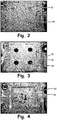
- FIG. 2 is a top view photograph of substrate 30 on which four stud bumps 32 are mounted in preparation for bonding an ASIC to substrate 30 (step 14 of FIG. 1 ).
- FIG. 3 is a top view photograph of substrate 30 on which silicone adhesive dots 34 are placed on stud bumps 32 (step 16 of FIG. 1 ).
- FIG. 4 is a top view photograph of substrate 30 in which ASIC 36 is placed on stud bumps 32 and silicone adhesive dots 34 (not visible in FIG. 4 ) (step 18 of FIG. 1 ).
- ASIC 36 is about 150 mils (3.8 mm) on a side.
- FIG. 5 is a side view photograph of substrate 30 showing the stand-off height between substrate 30 and ASIC 36 provided by stud bumps 32 (not visible in FIG. 5 ) and silicone adhesive dots 34 that laterally surround the stud bumps. Wire bonds 38 are provided to make electrical contacts from ASIC 36 to substrate 30.
- FIG. 6 is a scanning electron micrograph of multiple stud bumps formed on a substrate, to illustrate possible stand-off heights that can be achieved by stacking multiple stud bumps on top of one another.
- each stud bump may be formed from 1 mil (25.4 microns) gold wires and may be bonded to a substrate by a thermosonic ball bonder.
- multiple stud bump 40 is formed by vertically stacking two stud bumps, thereby providing a stand-off height of 2 mils (50.8 microns)
- multiple stud bump 42 is formed by vertically stacking three stud bumps, thereby providing a stand-off height of 3 mils (76.2 microns).
- the total stand-off height provided by the stud bumps may be from 1 mils (25.4 microns) to 10 mils (254 microns). In other embodiments, the total stand-off height provided by the stud bumps may be from 2 mils (50.8 microns) to 4 mils (101.6 microns). In some embodiment, the stud bumps may be from 1 mil (25.4 microns) to 10 mils (254 microns) in diameter. In other embodiments, the stud bumps may be from 2 mils (50.8 microns) to 4 mils (101.6 microns) in diameter.
- a method of attaching an integrated circuit to a substrate with a controlled stand-off height may include: mounting a plurality of stud bumps of the controlled stand-off height to the substrate at predetermined locations; placing adhesive dots over the stud bumps; placing the integrated circuit on the substrate over the adhesive dots; applying downward pressure on the integrated circuit until the integrated circuit is in mechanical contact with the stud bumps; and thermally curing the adhesive dots.
- the method of the preceding paragraph can optionally include, additionally and/or alternatively any, one or more of the following features, configurations and/or additional components:
- the plurality of stud bumps may be made of gold.
- the controlled stand-off height may be 1 mil (25.4 microns) to 10 mils (254 microns).
- the controlled stand-off height may be 2 mils (50.8 microns) to 4 mils (101.6 microns).
- the plurality of stud bumps may be 1 mil (25.4 microns) to 10 mils (254 microns) in diameter.
- the plurality of stud bumps may be 2 mils (50.8 microns) to 4 mils (101.6 microns) in diameter.
- the adhesive dots may be silicone adhesive dots.
- Thermally curing the adhesive may include heating to about 302°F (150°C).
- An attachment feature for an integrated circuit on a substrate that provides a controlled stand-off height may include: a plurality of stud bumps on the substrate; and a plurality of adhesive dots covering the stud bumps; wherein the plurality of stud bumps and plurality of adhesive dots on the substrate may be configured to attach the integrated circuit to the substrate at the controlled stand-off height determined by heights of the stud bumps upon pressing down of the integrated circuit on the adhesive dots to achieve physical contact between the substrate and the stud bumps.
- the plurality of stud bumps may include multiple stud bumps stacked on top of one another.
- the plurality of stud bumps may be made of gold.
- the controlled stand-off height may be 1 mil (25.4 microns) to 10 mils (254 microns).
- the controlled stand-of height may be 2 mils (50.8 microns) to 4 mils (101.6 microns).
- the plurality of stud bumps may be 1 mil (25.4 microns) to 10 mils (254 microns) in diameter.
- the plurality of stud bumps may be 2 mils (50.8 microns) to 4 mils (101.6 microns) in diameter.
- the plurality of adhesive dots may be silicone adhesive dots.
Landscapes
- Wire Bonding (AREA)
- Adhesives Or Adhesive Processes (AREA)
Abstract


Description
- A number of issues affect the performance of a high density microelectronic package. Many of these are related to die attach technology. One example is thermal management, and particularly concerns over thermal heating and stress due to differences in the coefficient of thermal expansion (CTE) in different adjacent materials assembled in the package. Internal stress at the chip level as well as at the circuit board level can affect the electronic performance of a microelectronic package.
- MEMS and IC devices may require stress relief for die attach at the device level as well as at the board level. Stress relief may be achieved by mechanical compliance at the attachment points. Examples of mechanically compliant adhesives are silicones, epoxies, and polyimides. Silicone adhesives are popular compliant prior art die and board attach adhesives and may be employed in the form of silicone dots positioned at attachment points. If stand-off is an issue, silicone dots alone may not control the stand-off of a device from a substrate. If the stand-off provided by the silicone dots varies, the stress imparted to the die or board may vary by how much silicone touches the back side of the device. A prior art method to control the stand-off height is to incorporate glass beads in the silicone adhesive. An improved method to control the stand-off with silicone dot adhesives for die attach would be helpful.
- An integrated circuit is attached to a substrate with a controlled stand-off height, by mounting a plurality of stud bumps of the controlled stand-off height to the substrate at predetermined locations, placing adhesive dots over the stud bumps, placing the integrated circuit on the substrate over the adhesive dots, and applying downward pressure on the integrated circuit until the integrated circuit is in mechanical contact with the stud bumps.
- An attachment feature for an integrated circuit on a substrate provides a controlled stand-off height. The attachment feature includes a plurality of stud bumps on the substrate, and a plurality of adhesive dots covering the stud bumps. The plurality of stud bumps and the plurality of adhesive dots on the substrate are configured to attach the integrated circuit to the substrate at the controlled stand-off height determined by heights of the stud bumps upon pressing down of the integrated circuit on the adhesive dots to achieve physical contact between the substrate and the stud bumps.
-
-
FIG. 1 is a flow diagram of a die attach process using stud bumps. -
FIG. 2 is a top view photograph of a substrate with stud bumps mounted on the substrate. -
FIG. 3 is a top view photograph of the substrate with silicone dots over the stud bumps. -
FIG. 4 is a top view photograph of an ASIC placed on top of the silicone dots and stud bumps on the substrate. -
FIG. 5 is a side view photograph of the ASIC showing the stand-off height and wire bonds. -
FIG. 6 is a scanning electron micrograph of multiple stud bumps formed on a substrate, to illustrate possible stand-off heights that can be achieved by stacking multiple stud bumps on top of one another. - A non-limiting method to control the stand-off distance during die attach of a MEMS, IC or circuit board to a substrate is to insert a rigid core with a specific height in the adhesive before attachment. In an embodiment, the rigid core of the present disclosure may be a stud bump. The stud bumps may be formed using any stud bumping machine and method known in the art. An example of a stud bumping operation may include melting an end of a wire of a desired stud bump material to form a ball on the end of the wire. The stud bumping apparatus may then bond the ball onto a package substrate. The wire is then cut close to the ball, leaving the stud bump. The total height of the stud bumps may be varied by adding stud bumps to the initial stud bump until a predetermined stand-off height is reached.
-
FIG. 1 is a flow diagram of dieattach assembly process 10 using stud bumps. First, a suitable substrate is acquired (step 12). Stud bumps may then be mounted on the substrate at predetermined positions on the substrate at predetermined heights (step 14). Next, silicone adhesive dots may be placed on the stud bumps (step 16). In other embodiments, other polymer adhesives known in the art may be used. In an embodiment an application specific integrated circuit (ASIC) may then be placed on the substrate containing the stud bumps and silicone adhesive dots (step 18). The ASIC may be pressed down to cause physical contact between the ASIC and the stud bumps, with the silicon adhesive dots being forced to the sides to laterally surround the location where the ASIC and the stud bumps contact one another. The stud bumps and silicone adhesive dots together provide adhesion (due to the silicon adhesive dots) and a consistent stand-off height (due to the stud bumps) between the substrate and the ASIC attached thereto. The silicone adhesive may then be thermally cured by heating the assembly to about 150° C (step 20). In the last step, wire bonds may then be made from the ASIC to contacts on the substrate (step 20). -
FIG. 2 is a top view photograph ofsubstrate 30 on which fourstud bumps 32 are mounted in preparation for bonding an ASIC to substrate 30 (step 14 ofFIG. 1 ).FIG. 3 is a top view photograph ofsubstrate 30 on which siliconeadhesive dots 34 are placed on stud bumps 32 (step 16 ofFIG. 1 ).FIG. 4 is a top view photograph ofsubstrate 30 in which ASIC 36 is placed onstud bumps 32 and silicone adhesive dots 34 (not visible inFIG. 4 ) (step 18 ofFIG. 1 ). In an exemplary embodiment, ASIC 36 is about 150 mils (3.8 mm) on a side.FIG. 5 is a side view photograph ofsubstrate 30 showing the stand-off height betweensubstrate 30 andASIC 36 provided by stud bumps 32 (not visible inFIG. 5 ) and siliconeadhesive dots 34 that laterally surround the stud bumps.Wire bonds 38 are provided to make electrical contacts from ASIC 36 tosubstrate 30. -
FIG. 6 is a scanning electron micrograph of multiple stud bumps formed on a substrate, to illustrate possible stand-off heights that can be achieved by stacking multiple stud bumps on top of one another. In an exemplary embodiment, each stud bump may be formed from 1 mil (25.4 microns) gold wires and may be bonded to a substrate by a thermosonic ball bonder. As shown inFIG. 6 ,multiple stud bump 40 is formed by vertically stacking two stud bumps, thereby providing a stand-off height of 2 mils (50.8 microns), andmultiple stud bump 42 is formed by vertically stacking three stud bumps, thereby providing a stand-off height of 3 mils (76.2 microns). In some embodiments, the total stand-off height provided by the stud bumps may be from 1 mils (25.4 microns) to 10 mils (254 microns). In other embodiments, the total stand-off height provided by the stud bumps may be from 2 mils (50.8 microns) to 4 mils (101.6 microns). In some embodiment, the stud bumps may be from 1 mil (25.4 microns) to 10 mils (254 microns) in diameter. In other embodiments, the stud bumps may be from 2 mils (50.8 microns) to 4 mils (101.6 microns) in diameter. - As a result of providing stud bumps on a substrate in the regions of silicone adhesive (such as gold stud bumps in an exemplary embodiment), consistent stand-off heights and locations can be provided through the use of auto ball bonders, without the need for special mixtures of glass beads and silicone adhesives. Consistent stand-off heights and repeatable contact area of silicone adhesive to a device (such as an ASIC) minimize stress and geometric variations in the electrical performance of the device. Wire bond connections to the device are also improved due to the Z axis stiffness provided by the stud bumps.
- The following are non-exclusive descriptions of possible embodiments of the present invention.
- A method of attaching an integrated circuit to a substrate with a controlled stand-off height may include: mounting a plurality of stud bumps of the controlled stand-off height to the substrate at predetermined locations; placing adhesive dots over the stud bumps; placing the integrated circuit on the substrate over the adhesive dots; applying downward pressure on the integrated circuit until the integrated circuit is in mechanical contact with the stud bumps; and thermally curing the adhesive dots.
- The method of the preceding paragraph can optionally include, additionally and/or alternatively any, one or more of the following features, configurations and/or additional components:
- The plurality of stud bumps may include multiple stud bumps stacked on top of one another at the predetermined locations.
- The plurality of stud bumps may be made of gold.
- The controlled stand-off height may be 1 mil (25.4 microns) to 10 mils (254 microns).
- The controlled stand-off height may be 2 mils (50.8 microns) to 4 mils (101.6 microns).
- The plurality of stud bumps may be 1 mil (25.4 microns) to 10 mils (254 microns) in diameter.
- The plurality of stud bumps may be 2 mils (50.8 microns) to 4 mils (101.6 microns) in diameter.
- The adhesive dots may be silicone adhesive dots.
- Thermally curing the adhesive may include heating to about 302°F (150°C).
- An attachment feature for an integrated circuit on a substrate that provides a controlled stand-off height may include: a plurality of stud bumps on the substrate; and a plurality of adhesive dots covering the stud bumps; wherein the plurality of stud bumps and plurality of adhesive dots on the substrate may be configured to attach the integrated circuit to the substrate at the controlled stand-off height determined by heights of the stud bumps upon pressing down of the integrated circuit on the adhesive dots to achieve physical contact between the substrate and the stud bumps.
- The feature of the preceding paragraph can optionally include, additionally and/or alternatively any, one or more of the following features, configurations and/or additional components:
- The plurality of stud bumps may include multiple stud bumps stacked on top of one another.
- The plurality of stud bumps may be made of gold.
- The controlled stand-off height may be 1 mil (25.4 microns) to 10 mils (254 microns).
- The controlled stand-of height may be 2 mils (50.8 microns) to 4 mils (101.6 microns).
- The plurality of stud bumps may be 1 mil (25.4 microns) to 10 mils (254 microns) in diameter.
- The plurality of stud bumps may be 2 mils (50.8 microns) to 4 mils (101.6 microns) in diameter.
- The plurality of adhesive dots may be silicone adhesive dots.
- While the invention has been described with reference to an exemplary embodiment(s), it will be understood by those skilled in the art that various changes may be made and equivalents may be substituted for elements thereof without departing from the scope of the invention. In addition, many modifications may be made to adapt a particular situation or material to the teachings of the invention without departing from the essential scope thereof. Therefore, it is intended that the invention not be limited to the particular embodiment(s) disclosed, but that the invention will include all embodiments falling within the scope of the appended claims.
Claims (15)
- A method of attaching an integrated circuit (36) to a substrate (30) with a controlled stand-off height, the method comprising:mounting a plurality of stud bumps (32) of the controlled stand-off height to the substrate (30) at predetermined locations;placing adhesive dots (34) over the stud bumps (32);placing the integrated circuit (36) on the substrate (30) over the adhesive dots (34);applying downward pressure on the integrated circuit (36) until the integrated circuit is in mechanical contact with the stud bumps (32); andthermally curing the adhesive dots (34).
- The method of claim 1, wherein the plurality of stud bumps (32) includes multiple stud bumps (32) stacked on top of one another at the predetermined locations.
- The method of claim 1, wherein the plurality of stud bumps (32) are made of gold.
- The method of claim 1, wherein the controlled stand-off height is 1 mil (25.4 microns) to 10 mils (254 microns), and wherein preferably the controlled stand-off height is 2 mils (50.8 microns) to 4 mils (101.6 microns).
- The method of any preceding claim, wherein the plurality of stud bumps (32) are 1 mil (25.4 microns) to 10 mils (254 microns) in diameter.
- The method of claim 5, wherein the plurality of stud bumps (32) are 2 mils (50.8 microns) to 4 mils (101.6 microns) in diameter.
- The method of any preceding claim, wherein the adhesive dots (34) are silicone adhesive dots.
- The method of claim 7 wherein thermally curing the adhesive dots (34) comprises heating to about 302°F (150°C).
- An attachment feature for an integrated circuit (36) on a substrate (30) that provides a controlled stand-off height, comprising:a plurality of stud bumps (32) on the substrate (30); anda plurality of adhesive dots (34) covering the stud bumps (32);wherein the plurality of stud bumps (32) and the plurality of adhesive dots (34) on the substrate (30) are configured to attach the integrated circuit (36) to the substrate (30) at the controlled stand-off height determined by heights of the stud bumps (32) upon pressing down of the integrated circuit (36) on the adhesive dots (34) to achieve physical contact between the substrate (30) and the stud bumps (32).
- The feature of claim 9, wherein the plurality of stud bumps (32) includes multiple stud bumps (32) stacked on top of one another.
- The feature of claim 9 or 10, wherein the plurality of stud bumps (32) are made of gold.
- The feature of claim 9, 10 or 11, wherein the controlled stand-off height is 1 mil (25.4 microns) to 10 mils (254 microns), and wherein preferably the controlled stand-off height is 2 mils (50.8 microns) to 4 mils (101.6 microns).
- The feature of any of claims 9 to 12, wherein the plurality of stud bumps (32) are 1 mil (25.4 microns) to 10 mils (254 microns) in diameter.
- The feature of claim 13, wherein the plurality of stud bumps (32) are 2 mils (50.8 microns) to 4 mils (101.6 microns) in diameter.
- The feature of any of claims 9 to 14, wherein the plurality of adhesive dots (34) are silicone adhesive dots.
Applications Claiming Priority (1)
| Application Number | Priority Date | Filing Date | Title |
|---|---|---|---|
| US15/151,160 US9754914B1 (en) | 2016-05-10 | 2016-05-10 | Method to provide die attach stress relief using gold stud bumps |
Publications (1)
| Publication Number | Publication Date |
|---|---|
| EP3244445A1 true EP3244445A1 (en) | 2017-11-15 |
Family
ID=58548569
Family Applications (1)
| Application Number | Title | Priority Date | Filing Date |
|---|---|---|---|
| EP17166195.2A Withdrawn EP3244445A1 (en) | 2016-05-10 | 2017-04-12 | Method to provide die attach stress relief using gold stud bumps |
Country Status (4)
| Country | Link |
|---|---|
| US (1) | US9754914B1 (en) |
| EP (1) | EP3244445A1 (en) |
| BR (1) | BR102017006202B1 (en) |
| CA (1) | CA2957999A1 (en) |
Citations (5)
| Publication number | Priority date | Publication date | Assignee | Title |
|---|---|---|---|---|
| JPH09306953A (en) * | 1996-05-10 | 1997-11-28 | Aisin Aw Co Ltd | Bare chip mounted semiconductor device and manufacturing method thereof |
| GB2339332A (en) * | 1998-07-08 | 2000-01-19 | Infrared Integrated Syst Ltd | Assembling planar electrical components |
| KR20050008121A (en) * | 2003-07-14 | 2005-01-21 | 주식회사 에이엠아이 씨 | Solid-State Imaging Apparatus and Method For Manufacturing The Same |
| JP2011258794A (en) * | 2010-06-10 | 2011-12-22 | Denso Corp | Electronic apparatus and method of manufacturing the same |
| JP2013110188A (en) * | 2011-11-18 | 2013-06-06 | Semiconductor Components Industries Llc | Semiconductor device and manufacturing method of the same |
Family Cites Families (16)
| Publication number | Priority date | Publication date | Assignee | Title |
|---|---|---|---|---|
| US6223429B1 (en) * | 1995-06-13 | 2001-05-01 | Hitachi Chemical Company, Ltd. | Method of production of semiconductor device |
| KR100352865B1 (en) * | 1998-04-07 | 2002-09-16 | 신꼬오덴기 고교 가부시키가이샤 | Semiconductor device and method for manufacturing the same |
| US5969461A (en) * | 1998-04-08 | 1999-10-19 | Cts Corporation | Surface acoustic wave device package and method |
| US6784541B2 (en) * | 2000-01-27 | 2004-08-31 | Hitachi, Ltd. | Semiconductor module and mounting method for same |
| US6297562B1 (en) * | 1999-09-20 | 2001-10-02 | Telefonaktieboalget Lm Ericsson (Publ) | Semiconductive chip having a bond pad located on an active device |
| EP1603170B1 (en) * | 2003-03-10 | 2018-08-01 | Toyoda Gosei Co., Ltd. | Method for manufacturing a solid-state optical element device |
| US6856009B2 (en) * | 2003-03-11 | 2005-02-15 | Micron Technology, Inc. | Techniques for packaging multiple device components |
| US7118389B2 (en) * | 2004-06-18 | 2006-10-10 | Palo Alto Research Center Incorporated | Stud bump socket |
| US7754507B2 (en) * | 2005-06-09 | 2010-07-13 | Philips Lumileds Lighting Company, Llc | Method of removing the growth substrate of a semiconductor light emitting device |
| US7838988B1 (en) | 2009-05-28 | 2010-11-23 | Texas Instruments Incorporated | Stud bumps as local heat sinks during transient power operations |
| US7880287B1 (en) | 2009-08-07 | 2011-02-01 | Triquint Semiconductor, Inc. | Stud bumps for die alignment |
| US8884431B2 (en) * | 2011-09-09 | 2014-11-11 | Taiwan Semiconductor Manufacturing Company, Ltd. | Packaging methods and structures for semiconductor devices |
| US9351436B2 (en) * | 2013-03-08 | 2016-05-24 | Cochlear Limited | Stud bump bonding in implantable medical devices |
| US9299671B2 (en) * | 2013-10-15 | 2016-03-29 | Invensense, Inc. | Integrated CMOS back cavity acoustic transducer and the method of producing the same |
| TWI538762B (en) * | 2014-01-03 | 2016-06-21 | 樂金股份有限公司 | Solder ball bump and package structure and method of forming same |
| US10319890B2 (en) * | 2015-01-26 | 2019-06-11 | Cooledge Lighting Inc. | Systems for adhesive bonding of electronic devices |
-
2016
- 2016-05-10 US US15/151,160 patent/US9754914B1/en active Active
-
2017
- 2017-02-14 CA CA2957999A patent/CA2957999A1/en active Pending
- 2017-03-27 BR BR102017006202-3A patent/BR102017006202B1/en active IP Right Grant
- 2017-04-12 EP EP17166195.2A patent/EP3244445A1/en not_active Withdrawn
Patent Citations (5)
| Publication number | Priority date | Publication date | Assignee | Title |
|---|---|---|---|---|
| JPH09306953A (en) * | 1996-05-10 | 1997-11-28 | Aisin Aw Co Ltd | Bare chip mounted semiconductor device and manufacturing method thereof |
| GB2339332A (en) * | 1998-07-08 | 2000-01-19 | Infrared Integrated Syst Ltd | Assembling planar electrical components |
| KR20050008121A (en) * | 2003-07-14 | 2005-01-21 | 주식회사 에이엠아이 씨 | Solid-State Imaging Apparatus and Method For Manufacturing The Same |
| JP2011258794A (en) * | 2010-06-10 | 2011-12-22 | Denso Corp | Electronic apparatus and method of manufacturing the same |
| JP2013110188A (en) * | 2011-11-18 | 2013-06-06 | Semiconductor Components Industries Llc | Semiconductor device and manufacturing method of the same |
Non-Patent Citations (1)
| Title |
|---|
| JONG-KAI LIN: "LOW THERMO-MECHANICAL STRESS FLIP CHIP BUMPS", MOTOROLA TECHNICAL DEVELOPMENTS, MOTOROLA INC. SCHAUMBURG, ILLINOIS, US, vol. 18, 1 March 1993 (1993-03-01), pages 76 - 77, XP000349565, ISSN: 0887-5286 * |
Also Published As
| Publication number | Publication date |
|---|---|
| US9754914B1 (en) | 2017-09-05 |
| BR102017006202A2 (en) | 2017-11-28 |
| BR102017006202B1 (en) | 2023-03-07 |
| CA2957999A1 (en) | 2017-11-10 |
Similar Documents
| Publication | Publication Date | Title |
|---|---|---|
| CN100390990C (en) | Stacked multi-chip package and method of manufacturing stacked multi-chip package | |
| TWI588949B (en) | Microelectronic package with integrated carrier surface | |
| US10008477B2 (en) | Microelectronic element with bond elements to encapsulation surface | |
| US6476503B1 (en) | Semiconductor device having columnar electrode and method of manufacturing same | |
| US5773896A (en) | Semiconductor device having offsetchips | |
| US7238548B2 (en) | Flip-chip type semiconductor device, production process for manufacturing such flip-chip type semiconductor device, and production process for manufacturing electronic product using such flip-chip type semiconductor device | |
| US8058717B2 (en) | Laminated body of semiconductor chips including pads mutually connected to conductive member | |
| WO2010070806A1 (en) | Semiconductor device, flip-chip mounting method and flip-chip mounting apparatus | |
| CN105621343A (en) | Package for semiconductor devices sensitive to mechanical and thermo-mechanical stresses, such as MEMS pressure sensors | |
| CN106206327A (en) | For the method and apparatus assembling semiconductor packages | |
| CN104340947A (en) | Assembly and packaging of MEMS device | |
| KR100698527B1 (en) | Chip stack package having pillar bumps using metal bumps and method for manufacturing same | |
| JP2012009655A (en) | Semiconductor package and method of manufacturing the semiconductor package | |
| CN103531581B (en) | Multi-chip module | |
| US20080185717A1 (en) | Semiconductor device including bump electrodes | |
| US8643159B2 (en) | Lead frame with grooved lead finger | |
| US9754914B1 (en) | Method to provide die attach stress relief using gold stud bumps | |
| JP4594777B2 (en) | Manufacturing method of multilayer electronic component | |
| JP2009246079A (en) | Semiconductor package and method of manufacturing the same | |
| US8927877B2 (en) | Looped interconnect structure | |
| KR101688077B1 (en) | Semiconductor package structure and manufacturing method thereof | |
| CN105742300A (en) | Chip package and method for fabricating the same | |
| JPH11204572A (en) | Semiconductor device mounting structure and method of manufacturing the same | |
| JP3973615B2 (en) | Manufacturing method of semiconductor device | |
| JPH1140697A (en) | Tape carrier for semiconductor device |
Legal Events
| Date | Code | Title | Description |
|---|---|---|---|
| PUAI | Public reference made under article 153(3) epc to a published international application that has entered the european phase |
Free format text: ORIGINAL CODE: 0009012 |
|
| STAA | Information on the status of an ep patent application or granted ep patent |
Free format text: STATUS: THE APPLICATION HAS BEEN PUBLISHED |
|
| AK | Designated contracting states |
Kind code of ref document: A1 Designated state(s): AL AT BE BG CH CY CZ DE DK EE ES FI FR GB GR HR HU IE IS IT LI LT LU LV MC MK MT NL NO PL PT RO RS SE SI SK SM TR |
|
| AX | Request for extension of the european patent |
Extension state: BA ME |
|
| STAA | Information on the status of an ep patent application or granted ep patent |
Free format text: STATUS: REQUEST FOR EXAMINATION WAS MADE |
|
| 17P | Request for examination filed |
Effective date: 20180515 |
|
| RBV | Designated contracting states (corrected) |
Designated state(s): AL AT BE BG CH CY CZ DE DK EE ES FI FR GB GR HR HU IE IS IT LI LT LU LV MC MK MT NL NO PL PT RO RS SE SI SK SM TR |
|
| STAA | Information on the status of an ep patent application or granted ep patent |
Free format text: STATUS: EXAMINATION IS IN PROGRESS |
|
| 17Q | First examination report despatched |
Effective date: 20220321 |
|
| STAA | Information on the status of an ep patent application or granted ep patent |
Free format text: STATUS: THE APPLICATION HAS BEEN WITHDRAWN |
|
| 18W | Application withdrawn |
Effective date: 20250207 |