EP3244416A1 - Memory and reference circuit calibration method thereof - Google Patents
Memory and reference circuit calibration method thereof Download PDFInfo
- Publication number
- EP3244416A1 EP3244416A1 EP17169809.5A EP17169809A EP3244416A1 EP 3244416 A1 EP3244416 A1 EP 3244416A1 EP 17169809 A EP17169809 A EP 17169809A EP 3244416 A1 EP3244416 A1 EP 3244416A1
- Authority
- EP
- European Patent Office
- Prior art keywords
- calibration
- current
- voltage
- connection terminal
- circuit
- Prior art date
- Legal status (The legal status is an assumption and is not a legal conclusion. Google has not performed a legal analysis and makes no representation as to the accuracy of the status listed.)
- Granted
Links
Images


Classifications
-
- G—PHYSICS
- G11—INFORMATION STORAGE
- G11C—STATIC STORES
- G11C5/00—Details of stores covered by group G11C11/00
- G11C5/14—Power supply arrangements, e.g. power down, chip selection or deselection, layout of wirings or power grids, or multiple supply levels
- G11C5/147—Voltage reference generators, voltage or current regulators; Internally lowered supply levels; Compensation for voltage drops
-
- G—PHYSICS
- G11—INFORMATION STORAGE
- G11C—STATIC STORES
- G11C16/00—Erasable programmable read-only memories
- G11C16/02—Erasable programmable read-only memories electrically programmable
- G11C16/06—Auxiliary circuits, e.g. for writing into memory
- G11C16/26—Sensing or reading circuits; Data output circuits
-
- G—PHYSICS
- G11—INFORMATION STORAGE
- G11C—STATIC STORES
- G11C29/00—Checking stores for correct operation ; Subsequent repair; Testing stores during standby or offline operation
- G11C29/02—Detection or location of defective auxiliary circuits, e.g. defective refresh counters
- G11C29/026—Detection or location of defective auxiliary circuits, e.g. defective refresh counters in sense amplifiers
-
- G—PHYSICS
- G11—INFORMATION STORAGE
- G11C—STATIC STORES
- G11C29/00—Checking stores for correct operation ; Subsequent repair; Testing stores during standby or offline operation
- G11C29/02—Detection or location of defective auxiliary circuits, e.g. defective refresh counters
- G11C29/028—Detection or location of defective auxiliary circuits, e.g. defective refresh counters with adaption or trimming of parameters
-
- G—PHYSICS
- G11—INFORMATION STORAGE
- G11C—STATIC STORES
- G11C7/00—Arrangements for writing information into, or reading information out from, a digital store
- G11C7/06—Sense amplifiers; Associated circuits, e.g. timing or triggering circuits
-
- G—PHYSICS
- G11—INFORMATION STORAGE
- G11C—STATIC STORES
- G11C7/00—Arrangements for writing information into, or reading information out from, a digital store
- G11C7/14—Dummy cell management; Sense reference voltage generators
Definitions
- the present invention generally relates to the field of semiconductor manufacturing technology and, more particularly, relates to a memory and reference circuit calibration method thereof.
- a flash memory uses the flash technology to achieve storage of electronic information.
- the flash memory has many advantages such as driverless, fast speed, small size, desired compatibility, and large capacity, etc., and, therefore, has been widely used.
- the flash memory can perform read and write, erase and copy operations on data. Different operations have different drive circuits.
- the data is stored in two forms, '1' and '0', which correspond to two basic memory cells, an erase cell and a program cell, respectively.
- the type of the memory cell first needs to be determined, whether it is the program cell or the erase cell.
- a sense amplifier (SA) circuit needs to be used.
- An array formed by the sense amplifier circuits is usually referred to as a sense array.
- a reference signal needs to be used. By comparing the reference signal and a signal outputted from the memory cell, the type of the memory cell can be determined. Therefore, the reference signal is important for the accuracy of a reading result.
- the reference signal is generated by a reference circuit.
- the design of the reference circuit directly impacts the output of the reference signal, and impacts the accuracy of the reading result.
- errors may easily occur in the reading result of the flash memory.
- the disclosed device structures and methods are directed to solve one or more problems set forth above and other problems.
- a first aspect of the present invention provides a memory.
- the memory includes a memory array including a plurality of memory cells, and a reference circuit including a reference memory cell and a reference connection terminal, wherein the reference memory cell is a same as the memory cell.
- the memory also includes a calibration circuit including a calibration connection terminal, and a mirror circuit including a first mirror terminal and a second mirror terminal, wherein the first mirror terminal is connected to the reference connection terminal, and the second mirror terminal is connected to the calibration connection terminal.
- the memory includes a clamp circuit, configured to set one of a voltage of the reference connection terminal and a voltage of the calibration connection terminal as a preset voltage and to set the other thereof as a comparison voltage.
- the memory includes a comparison circuit configured to input the comparison voltage and the preset voltage, and to output a comparison result.
- the mirror circuit includes: a first MOS transistor; and a second MOS transistor group, wherein a gate of the first MOS transistor is connected to a gate of the second MOS transistor group.
- the clamp circuit includes: an operational amplifier including a first operational input terminal, a second operational input terminal, and an operational output terminal, wherein the first operational input terminal is connected to one of the reference connection terminal and the calibration connection terminal, the second operational input terminal is configured to apply the preset voltage, and the operational output terminal is connected to the gate of the first MOS transistor.
- the comparison circuit includes: a comparison amplifier including a first comparison terminal, a second comparison terminal, and a comparison output terminal, wherein the first comparison terminal is connected to the other of the reference connection terminal and the calibration connection terminal, and the second comparison terminal is configured to apply the preset voltage.
- the calibration circuit includes: a plurality of calibration memory cells; a plurality of calibration word lines; and a plurality of calibration bit lines, wherein the calibration memory cell is a same as the memory cell, a plurality of the calibration memory cells are arranged to form a calibration memory array, the calibration memory cells in a same row of the calibration memory array share a same calibration word line, and the calibration memory cells in a same column of the calibration memory array share a same calibration bit line.
- the calibration memory array is a matrix with two rows and a plurality of columns.
- the memory further includes approximately 4-16 columns of the calibration memory array.
- a scaling factor of the mirror circuit is calculated by dividing the number of columns of the calibration memory array by a value of approximately 0.1-0.4.
- a second aspect of the present invention provides a reference circuit calibration method.
- the method includes providing a memory, and adjusting the clamp circuit to set one of the voltage of the reference connection terminal and the voltage of the calibration connection terminal as a preset voltage.
- the method also includes adjusting the calibration circuit to generate a second current from the calibration connection terminal.
- the method includes adjusting the reference circuit to perform a weak programming on the reference memory cell, and to generate a first current from the reference connection terminal, wherein when the voltage of the reference connection terminal is the preset voltage, through the mirror circuit, the calibration connection terminal generates a mirror current corresponding to the first current as well as a comparison voltage; and when the voltage of the calibration connection terminal is the preset voltage, through the mirror circuit, the reference connection terminal generates a mirror current corresponding to the second current as well as a comparison voltage. Further, the method includes outputting the reference current from the reference connection terminal when the comparison voltage is equal to the preset voltage, determined by the comparison circuit.
- the reference circuit also includes a reference word line and a reference bit line, wherein performing the weak programming on the reference memory cell includes adjusting a voltage applied onto the reference word line to output the first current from the reference bit line.
- adjusting the calibration circuit includes: programming a plurality of the calibration memory cells; erasing portions of the plurality of the calibration memory cells; selecting two calibration word lines; applying a voltages onto the two selected calibration word lines; and applying voltages onto a plurality of the calibration bit lines to output a plurality of calibration current from the plurality of the calibration bit lines, and to form the second current.
- erasing portions of the calibration memory cells includes: erasing the calibration memory cells in a calibration memory array with odd rows and odd columns; and erasing the calibration memory cells in the calibration memory array with even rows and even columns.
- selecting the two calibration word lines includes: selecting a calibration word line connecting to the calibration memory cells in the calibration memory array with an odd row; and selecting a calibration word line connecting to the calibration memory cells in the calibration memory array with an even row.
- the reference current is smaller than the calibration current.
- the calibration current is the same as the programming current.
- a ratio of the reference current over the calibration current is in a range of approximately 0.1-0.4.
- the voltages onto the plurality of the calibration bit lines approximately 4-16 calibration bit lines are applied with a voltage.
- adjusting the reference circuit includes: adjusting the voltage applied onto the reference word line to change the first current outputted from the reference bit line.
- adjusting the clamp circuit includes: applying the preset voltage onto a second operational input terminal of an operational amplifier.
- the method further includes: repeating the process of adjusting the reference circuit when the comparison voltage is unequal to the preset voltage.
- the memory of the first aspect of the present invention is preferably used or useable the method according to the second aspect of the present invention.
- a flash memory usually includes a reference circuit configured to generate a reference current, a memory cell configured to output a storage current, and a sense amplifier configured to input the storage current and the reference current and to output a reading result.
- the reference circuit includes a plurality of current sources and resistors connected in series. The reference current is generated by the current sources and the resistors.
- the current sources and the resistors do not change, or change in a different way from the memory cell. Therefore, it is easy to cause the reference current to be larger than the storage current outputted from the memory cell in a programming state, or to cause the reference current to be smaller than the storage current outputted from the memory cell in an erasing state, thus resulting in the occurrence of errors in the reading result.
- the present invention provides a memory and reference circuit calibration method.
- Figures 1-3 illustrate an exemplary memory consistent with the disclosed embodiments.
- the memory may include a memory array, a reference circuit 130, a calibration circuit 140, a mirror circuit 110, a clamp circuit 131, and a comparison circuit 120. Other components or circuits may also be included.
- the memory array may include a plurality of memory cells 111.
- the reference circuit 130 may include a reference memory cell and a reference connection terminal, and the reference memory cell may be the same as the memory cell 111.
- the calibration circuit 140 may include a calibration connection terminal.
- the mirror circuit 110 may include a first mirror terminal and a second mirror terminal.
- the first mirror terminal may be connected to the reference connection terminal of the reference circuit 130 and the second mirror terminal may be connected to the calibration connection terminal of the calibration circuit 140.
- the clamp circuit 131 may be configured to set the voltage of the reference connection terminal as a preset voltage, and to set the voltage of the calibration connection terminal as a comparison voltage. Or the clamp circuit 131 may be configured to set the voltage of the calibration connection terminal as a preset voltage, and to set the voltage of the reference connection terminal as a comparison voltage.
- the comparison circuit 120 may be configured to input the comparison voltage and the preset voltage, and to output a comparison result.
- the memory array may be configured to store digital information, and the memory cell 111 may be configured to output storage current.
- the memory array may include a plurality of the memory cells 111, and the memory cells 111 may be arranged in a matrix arrangement.
- the memory array may include program cells in a programming state and erase cells in an erasing state.
- the storage current outputted from the program cells may be programming current
- the storage current outputted from the erase cells may be erasing current.
- the memory array may also include a plurality of word lines and a plurality of bit lines. The word lines and the bit lines may be configured to control the programming and erasing of the memory cells.
- Figure 2 is a circuit schematic of the memory in Figure 1 consistent with the disclosed embodiments.
- the reference circuit 130 (shown in Figure 1 ) may be configured to output reference current.
- the reference current may be configured as a reference signal when data in the memory cell 111 (shown in Figure 1 ) is read.
- the reference circuit 130 may include the reference memory cell, and the reference memory cell may be the same as the memory cell 111. When the memory cell 111 changes due to impact of external environment, the reference memory cell may also undergo same changes as the memory cell 111.
- the reference memory cell may be configured for weak programming, and the outputted reference current may be smaller than the programming current.
- the reference memory cell may be configured for erasing, and the outputted reference current may be larger than the erasing current.
- a ratio of the reference current to the programming current may be in a range of approximately 0.1-0.4.
- the program cells may change due to a variety of factors, causing the programming process to be incomplete and the programming current to be small, the programming current may not be smaller than the reference current. Thus, read errors may be difficult to occur.
- the erase cells may change due to a variety of factors, causing the erasing current to be large, the erasing current may not be larger than the reference current. Thus, read errors may be difficult to occur.
- the reference circuit 130 may also include a reference word line REFWL connecting to a gate of the reference memory cell, and a reference bit line connecting to a source of the reference memory cell.
- the reference bit line may be configured to apply a voltage, and to generate the reference current from the reference memory cell.
- the reference word line may be configured to apply a reference word line voltage, and to control the magnitude of the reference current.
- the calibration circuit 140 may include a plurality of calibration memory cells.
- the calibration memory cells may be the same as the memory cells 111.
- the arrangement of the calibration memory cells may be the same as the arrangement of the memory cells 111.
- a plurality of the calibration memory cells may be arranged in a matrix arrangement to form a calibration memory array.
- the calibration circuit 140 may be configured to output second current.
- the second current may be similar to the programming current, and configured to calibrate the reference current, ensuring that the reference current may reach a preset value and be matched with the programming current. Therefore, read errors may be difficult to occur.
- the calibration circuit 140 may also include a plurality of calibration word lines WL and a plurality of calibration bit lines.
- the calibration memory cells in the same row of the calibration memory array may share a same calibration word line WL.
- the calibration memory cells in the same column of the calibration memory array may share a same calibration bit line.
- the calibration memory array may be a matrix with rows and columns. The number of columns of the calibration memory array may be in a range of approximately 4-16.
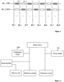
- Figure 3 is a schematic diagram of the calibration circuit 140 in Figure 2 .
- the calibration memory array may be a matrix with rows and eight columns.
- the calibration circuit 140 may include a plurality of the calibration word lines and eight calibration bit lines.
- the eight calibration bit lines may include a first calibration bit line BL1, a second calibration bit line BL2, a third calibration bit line BL3, a fourth calibration bit line BL4, a fifth calibration bit line BL5, a sixth calibration bit line BL6, a seventh calibration bit line BL7, and an eighth calibration bit line BL8.
- a plurality of the calibration word lines may include an odd calibration word line WL_ODD and an even calibration word line WL_EVEN.
- the calibration memory cells may include calibration program cells 32 configured for programming and calibration erase cells 31 configured for erasing.
- the mirror circuit 110 may include the first mirror terminal and the second mirror terminal.
- the first mirror terminal may be connected to the reference connection terminal 10, and be configured to generate the reference current.
- the second mirror terminal may be connected to the calibration connection terminal 20, and be configured to generate mirror current.
- a scaling factor of the mirror circuit 110 may be the ratio of the mirror current to the reference current.
- the scaling factor of the mirror circuit 110 may be calculated by dividing the number of the columns of the calibration memory array by a value of approximately 0.1-0.4, and be configured to ensure the ratio of the reference current to the programming current is in a range of approximately 0.1-0.4.
- the number of the columns of the calibration memory array may be eight, therefore the scaling factor of the mirror circuit 110 may be in a range of approximately 20-80.
- the mirror circuit 110 may include a first MOS transistor A and a second MOS transistor group B.
- a gate of the first MOS transistor may be connected to a gate of the second MOS transistor group B.
- the first MOS transistor A may be a single MOS transistor, and gain of the first MOS transistor may be 1.
- gate current of the first MOS transistor may be the same as the current flowing through the reference connection terminal 10.
- the gate current of the first MOS transistor may be different from the current flowing through the reference connection terminal 10.
- the second MOS transistor group B may be a MOS transistor group formed by a cascade of a plurality of MOS transistors. In certain embodiments, the second MOS transistor group B may also be a single MOS transistor. In one embodiment, the gate of the second MOS transistor group B may be connected to the gate of the first MOS transistor A to form the mirror circuit 110.
- the voltage of the calibration connection terminal 20 when the mirror current is equal to the second current, the voltage of the calibration connection terminal 20 may be equal to the voltage of the reference connection terminal 10. When the mirror current is larger than the second current, the voltage of the calibration connection terminal 20 may be larger than the voltage of the reference connection terminal 10. When the mirror current is smaller than the second current, the voltage of the calibration connection terminal 20 may be smaller than the voltage of the reference connection terminal 10.
- the clamp circuit 131 may be configured to set the voltage of the reference connection terminal 10 as a preset voltage V REF , and to set the voltage of the calibration connection terminal 20 as a comparison voltage. Or the clamp circuit 131 may be configured to set the voltage of the calibration connection terminal 20 as the preset voltage V REF , and to set the voltage of the reference connection terminal 10 as the comparison voltage.
- the clamp circuit 131 may include an operational amplifier C1.
- the operational amplifier C1 may include a first operational input terminal, a second operational input terminal, and an operational output terminal.
- the first operational input terminal may be connected to the reference connection terminal 10.
- the second operational input terminal may be configured to apply the preset voltage V REF .
- the operational output terminal may be connected to the gate of the first MOS transistor. Therefore, in one embodiment, the voltage of the reference connection terminal 10 may be the preset voltage V REF , and the voltage of the calibration connection terminal 20 may be the comparison voltage.
- the comparison voltage When the mirror current is equal to the second current, the comparison voltage may be equal to the preset voltage V REF . When the mirror current is larger than the second current, the comparison voltage may be larger than the preset voltage V REF . When the mirror current is smaller than the second current, the comparison voltage may be smaller than the preset voltage V REF .
- the comparison circuit 120 may include a comparison amplifier C2.
- the comparison amplifier C2 may include a first comparison terminal, a second comparison terminal, and a comparison output terminal SCOUT.
- the first comparison terminal may be connected to the calibration connection terminal 20, and the second comparison terminal may be configured to apply the preset voltage V REF .
- the comparison result outputted from the comparison circuit 120 when the comparison voltage is larger than the preset voltage V REF , the comparison result outputted from the comparison circuit 120 may be high level' '1'. When the comparison voltage is smaller than the preset voltage V REF , the comparison result outputted from the comparison circuit 120 may be low level '0'. In certain embodiments, when the comparison voltage is larger than the preset voltage V REF , the comparison result outputted from the comparison circuit 120 may be low level '0'. When the comparison voltage is smaller than the preset voltage V REF , the comparison result outputted from the comparison circuit 120 may be high level '1'.
- the memory may also include a sense amplifier 150 (shown in Figure 1 ).
- the sense amplifier 150 may be configured to input the storage current and the reference current, and to output the reading result.
- the sense amplifier 150 may include a first input terminal, a second input terminal and an output terminal.
- the first input terminal may be configured to input the reference current.
- the second input terminal may be configured to input the storage current.
- the output terminal may be configured to output the reading result.
- the sense amplifier 150 when the storage current is larger than the reference current, the sense amplifier 150 may output high level' '1'. When the storage current is smaller than the reference current, the sense amplifier 150 may output low level '0'.
- Figure 4 illustrates another exemplary memory consistent with the disclosed embodiments.
- the same or similar features of Figure 4 and Figure 1 are not repeated herein.
- the difference may include that in one embodiment, the clamp circuit 231 may be configured to set the voltage of the calibration connection terminal as the preset voltage, and to set the voltage of the reference connection terminal as the comparison voltage.
- the clamp circuit 231 may include an operational amplifier.
- the operational amplifier may include a first operational input terminal, a second operational input terminal, and an operational output terminal.
- the first operational input terminal may be connected to the calibration connection terminal.
- the second operational input terminal may be configured to apply the preset voltage.
- the operational output terminal may be connected to the gate of the first MOS transistor.
- the comparison circuit 220 may include a comparison amplifier.
- the comparison amplifier may include a first comparison terminal, a second comparison terminal, and a comparison output terminal SCOUT.
- the first comparison terminal may be connected to the reference connection terminal.
- the second comparison terminal may be configured to apply the preset voltage.
- the reference circuit may include the reference memory cell.
- the reference memory cell may be the same as the memory cell.
- the memory cell may change due to a variety of factors,, the reference memory cell may undergo same changes as the memory cell. Therefore, the magnitude relationship between the current flowing through the reference circuit and the current flowing through the memory cell may be difficult to change, the probability of occurring read errors in the memory may be further reduced. Thus, read errors may be difficult to occur in the memory consistent with disclosed embodiments.
- the calibration circuit may include calibration memory cells with rows and columns.
- the calibration memory cell may be the same as the memory cell.
- the calibration circuit may output the second current similar to the current outputted from the memory cells in the programming state, ensuring that the reference current may be matched with the current outputted from the memory cells in the programming state. Therefore, read errors may be difficult to occur in the memory.
- FIG. 5 illustrates an exemplary calibration process to calibrate the reference circuit of the memory consistent with the disclosed embodiments.
- a memory may be provided in Step S1 of the calibration process.
- the clamp circuit may be adjusted to set the voltage of the reference connection terminal or the voltage of the calibration connection terminal as the preset voltage.
- the calibration circuit may be adjusted to generate the second current from the calibration connection terminal.
- the reference circuit may be adjusted to perform a weak programming on the reference memory cell, and to generate the first current from the reference connection terminal.
- the calibration connection terminal may generate the mirror current corresponding to the first current as well as the comparison voltage.
- the reference connection terminal may generate the mirror current corresponding to the second current as well as the comparison voltage.
- the comparison circuit may be configured to determine whether the comparison voltage is equal to the preset voltage.
- the reference connection terminal may output the reference current.
- the Step 4 of adjusting the reference circuit may be repeated.
- a memory may be provided (e.g. in Step S1).
- the memory may include a memory array, a reference circuit 130, a calibration circuit 140, a mirror circuit 110, a clamp circuit 131, a comparison circuit 120, and a sense amplifier 150.
- the memory array may include a plurality of memory cells 111 configured to output storage current.
- the reference circuit 130 may include a reference memory cell and a reference connection terminal, and the reference memory cell may be the same as the memory cell 111.
- the calibration circuit 140 may include a calibration connection terminal configured to generate second current.
- the mirror circuit 110 may include a first mirror terminal and a second mirror terminal. The first mirror terminal may be connected to the reference connection terminal of the reference circuit 130 and the second mirror terminal may be connected to the calibration connection terminal of the calibration circuit 140.
- the clamp circuit 131 may be configured to set the voltage of the reference connection terminal as a preset voltage V REF , and to set the voltage of the calibration connection terminal as a comparison voltage.
- the clamp circuit 131 may be configured to set the voltage of the calibration connection terminal as the preset voltage V REF , and to set the voltage of the reference connection terminal as the comparison voltage.
- the comparison circuit 120 may be configured to input the comparison voltage and the preset voltage V REF , and to output a comparison result.
- the sense amplifier 150 may be configured to input the storage current and the reference current, and to output a reading result.
- the memory array may include program cells in a programming state and erase cells in an erasing state.
- the storage current outputted from the program cells may be programming current
- the storage current outputted from the erase cells may be erasing current.
- Figure 2 is a circuit schematic of the memory in Figure 1 consistent with the disclosed embodiments.
- the mirror circuit 110 may include a first MOS transistor A and a second MOS transistor group B.
- a gate of the first MOS transistor A may be connected to a gate of the second MOS transistor group B.
- the clamp circuit 131 may include an operational amplifier C1.
- the operational amplifier C1 may include a first operational input terminal, a second operational input terminal, and an operational output terminal.
- the operational output terminal may be connected to the gate of the first MOS transistor A.
- the first operational input terminal may be connected to the reference connection terminal 10 or the calibration connection terminal 20.
- the second operational input terminal may be configured to apply the preset voltage V REF .
- the calibration circuit 140 may include a plurality of calibration memory cells, a plurality of calibration word lines and a plurality of calibration bit lines.
- a plurality of the calibration memory cells may be arranged to form a calibration memory array.
- the calibration memory cells in the same row of the calibration memory array may share a same calibration word line.
- the calibration memory cells in the same column of the calibration memory array may share a same calibration bit line.
- the calibration memory array may be a matrix with rows and eight columns.
- the calibration circuit 140 may include a plurality of the calibration word lines and eight calibration bit lines.
- the eight calibration bit lines may include a first calibration bit line BL1, a second calibration bit line BL2, a third calibration bit line BL3, a fourth calibration bit line BL4, a fifth calibration bit line BL5, a sixth calibration bit line BL6, a seventh calibration bit line BL7, and an eighth calibration bit line BL8.
- the comparison circuit 120 may include a comparison amplifier C2.
- the comparison amplifier C2 may include a first comparison terminal, a second comparison terminal, and a comparison output terminal SCOUT.
- the first comparison terminal may be connected to the calibration connection terminal 20.
- the second comparison terminal may be configured to apply the preset voltage V REF .
- the first comparison terminal may be connected to the reference connection terminal 10.
- the second comparison terminal may be configured to apply the preset voltage V REF .
- the clamp circuit 131 (shown in Figure 1 ) may be adjusted (e.g. in Step S2) to set one of the voltage of the reference connection terminal 10 and the voltage of the calibration connection terminal 20 as the preset voltage V REF .
- the clamp circuit 131 may be adjusted to set the voltage of the reference connection terminal 10 as the preset voltage V REF . In certain embodiments, the clamp circuit 131 may also be adjusted to set the voltage of the calibration connection terminal 20 as the preset voltage V REF .
- adjusting the clamp circuit 131 may include applying the preset voltage V REF on the second operational input terminal.
- the first operational input terminal of the operational amplifier C1 may be connected to the operational output terminal of the operational amplifier C1 through the first MOS transistor A to form a feedback loop, which can clamp the voltage of the reference connection terminal 10 at the preset voltage V REF .
- the calibration process may also include adjusting the comparison circuit (shown in Figure 1 ) to set the voltage of the second comparison input terminal as the preset voltage V REF .
- adjusting the comparison circuit 120 may include applying the preset voltage V REF on the second comparison input terminal of the comparison amplifier C2.
- the calibration circuit 140 may be adjusted (e.g. in Step S3) to generate the second current from the calibration connection terminal 20.
- adjusting the calibration circuit 140 may include performing a programming process on a plurality of the calibration memory cells to form calibration program cells 32; performing an erasing process on portions of the plurality of the calibration memory cells to form calibration erase cells 31; selecting two calibration word lines, where voltage may be applied onto the two selected calibration word lines and not be applied onto the other calibration word lines; and applying a voltage onto a plurality of the calibration bit lines to output a plurality of calibration current from the plurality of the calibration bit lines, thus to form the second current.
- erasing portions of the memory cells may include erasing the calibration memory cells in the calibration memory array with odd rows and odd columns; and erasing the calibration memory cells in the calibration memory array with even rows and even columns.
- erasing portions of the memory cells may include erasing the calibration memory cells in the calibration memory array with odd rows and even columns; and erasing the calibration memory cells in the calibration memory array with even rows and odd columns.
- selecting the two calibration word lines may include selecting an odd calibration word line WL_ODD connecting to the calibration memory cells in the calibration memory array with odd row; and selecting an even calibration word line WL_EVEN connecting to the calibration memory cells in the calibration memory array with the even row.
- a voltage may be applied onto a calibration bit line connecting to the calibration memory cells in the odd row and a calibration bit line connecting to the calibration memory cells in the even row.
- the second current may include current flowing through the memory cells in the even row and current flowing through the memory cells in the odd row. Therefore, the difference between the calibration current and the programming current caused by different positions of the selected calibration memory cells may be reduced, thus he calibration accuracy may be improved.
- the voltage applied to the odd calibration word line WL_ODD and the even calibration word line WL_EVEN may open a channel of the calibration program cells 32 and not open a channel of the calibration erase cells 31.
- voltage may be applied onto the odd calibration word line WL_ODD and the even calibration word line WL_EVEN and not be applied onto the other word lines, thus channels of the calibration memory cells connected to the other calibration word lines may not be opened. Therefore, in one embodiment, only the channel of the calibration program cells 32 connected to the odd calibration word line WL_ODD and the even calibration word line WL_EVEN may be opened.
- each bit line may include current only flowing through one calibration memory cell, thus the accuracy of the second current outputted from the calibration circuit may be improved.
- voltage may be applied onto the eight bit lines.
- the number of columns of the calibration memory cells may be larger than eight.
- Approximately 4-16 calibration bit lines may be applied with a voltage.
- voltage may be applied onto the first calibration bit line BL1, the second calibration bit line BL2, the third calibration bit line BL3, the fourth calibration bit line BL4, the fifth calibration bit line BL5, the sixth calibration bit line BL6, the seventh calibration bit line BL7, and the eighth calibration bit line BL8. Therefore, a plurality of the calibration bit lines may output eight calibration current, including a first bit line current, a second bit line current, a third bit line current, a fourth bit line current, a fifth bit line current, a sixth bit line current, a seventh bit line current, and an eighth bit line current.
- the current flowing through the selected calibration memory cells may easily deviate from the programming current due to the impact of environmental and other factors.
- Applying voltage onto a plurality of bit lines can reduce the impact of the environmental and other factors on the second current by combining the first bit line current, the second bit line current, the third bit line current, the fourth bit line current, the fifth bit line current, the sixth bit line current, the seventh bit line current, and the eighth bit line current, thus the calibration accuracy may be improved.
- the voltages applied onto the odd calibration word line WL_ODD and the even calibration word line WL_EVEN may be equal.
- the voltages applied onto the eight bit lines may be equal. Therefore, the first bit line current, the second bit line current, the third bit line current, the fourth bit line current, the fifth bit line current, the sixth bit line current, the seventh bit line current, and the eighth bit line current may be equal.
- the second current may be the sum of the first bit line current, the second bit line current, the third bit line current, the fourth bit line current, the fifth bit line current, the sixth bit line current, the seventh bit line current, and the eighth bit line current.
- the second current may be eight times of the calibration current.
- the mirror circuit 110 may include the first mirror terminal and the second mirror terminal.
- the first mirror terminal may be connected to the reference connection terminal 10 and be configured to input the reference current.
- the second mirror terminal may be connected to the calibration connection terminal 20 and be configured to output the mirror current.
- a scaling factor of the mirror circuit 110 may be a ratio of the mirror current to the reference current. In one embodiment, the scaling factor of the mirror circuit 110 may be calculated by dividing the number of the bit lines applied voltage by a value of approximately 0.1-0.4. For example, the scaling factor of the mirror circuit 110 may be in a range of approximately 20-80.
- the calibration current may be the same as the programming current.
- the ratio of the reference current to the programming current may be in a range of approximately 0.1-0.4.
- the program cells may change due to a variety of factors, causing the programming process to be incomplete and the programming current to be small, the programming current may not be smaller than the reference current, thus read errors may be difficult to occur.
- the erase cells may change due to a variety of factors, causing the erasing current to be large, the erasing current may not be larger than the reference current, thus read errors may be difficult to occur. Therefore, the ratio of the reference current to the programming current in a range of approximately 0.1-0.4 can reduce the probability of occurring read errors.
- the reference circuit 130 may be adjusted (e.g. in Step S4).
- a weak programming may be performed on the reference memory cell to generate the first current from the reference connection terminal 10.
- the calibration connection terminal 20 may generate the mirror current corresponding to the first current as well as the comparison voltage.
- the reference connection terminal 10 may generate the mirror current corresponding to the second current as well as the comparison voltage.
- adjusting the reference circuit 130 may include performing a weak programming on the reference memory cell.
- the reference circuit 130 may include a reference word line (REFWL) and a reference bit line.
- Performing a weak programming on the reference memory cell may include adjusting the voltage applied onto the reference word line (REFWL) to output the first current from the reference bit line.
- the reference memory cell may be the same as the memory cell.
- the reference memory cell may undergo same changes as the memory cell. Therefore, the magnitude relationship between t the current flowing through the reference circuit and the current flowing through the memory cell may be difficult to change, the probability of occurring the read errors in the memory may be further reduced. Thus, read errors in the memory consistent with disclosed embodiments may be difficult to occur.
- the comparison circuit 120 may be configured to determine whether the comparison voltage is equal to the preset voltage (e.g. in Step S5). When the comparison voltage is equal to the preset voltage, the reference connection terminal 10 may output the reference current (e.g. in Step S6). When the comparison voltage is unequal to the preset voltage, the process of adjusting the reference circuit 130 (e.g. in Step S4) may be repeated.
- the comparison voltage when the mirror current is larger than the second current, the comparison voltage may be larger than the preset voltage V REF , and the comparison amplifier C2 may output high level '1'.
- the comparison voltage When the mirror current is smaller than the second current, the comparison voltage may be smaller than the preset voltage V REF , and the comparison amplifier C2 may output low level '0'. Therefore, when the comparison result is in a falling edge or a rising edge, the comparison voltage may be equal to the preset voltage V REF , and the mirror current may be equal to the second current.
- the reference current may be equal to the second current divided by the scaling factor of the mirror circuit 110, thus the ratio of the reference current to the calibration current may be in a range of approximately 0.1-0.4, so as to obtain the required reference current.
- the second current may be generated at the calibration circuit, and the reference circuit may be adjusted.
- the reference connection terminal may output the reference current related to the second current. Therefore, the reference current may be matched with the second current, so as to achieve calibration of the reference circuit of the memory.
- Adjusting the reference circuit may include performing a weak programming on the reference memory cell. When the memory changes due to impact of external environment or the programming is incomplete, the reference memory cell may undergo same changes as the memory cell. Therefore, when the data in the memory cell is read, the magnitude relationship between the reference current and the current outputted from the memory cell may be difficult to change. Thus, read errors may be difficult to occur.
Landscapes
- Engineering & Computer Science (AREA)
- Power Engineering (AREA)
- Read Only Memory (AREA)
Abstract
Description
- This application claims the priority of Chinese patent application No.
201610315926.9, filed on May 12, 2016 - The present invention generally relates to the field of semiconductor manufacturing technology and, more particularly, relates to a memory and reference circuit calibration method thereof.
- A flash memory uses the flash technology to achieve storage of electronic information. The flash memory has many advantages such as driverless, fast speed, small size, desired compatibility, and large capacity, etc., and, therefore, has been widely used. The flash memory can perform read and write, erase and copy operations on data. Different operations have different drive circuits.
- In the flash memory, the data is stored in two forms, '1' and '0', which correspond to two basic memory cells, an erase cell and a program cell, respectively. When the data in the flash memory is read, the type of the memory cell first needs to be determined, whether it is the program cell or the erase cell. When determining the type of the memory cell, a sense amplifier (SA) circuit needs to be used. An array formed by the sense amplifier circuits is usually referred to as a sense array. When the sense amplifier circuit reads the data in the flash memory, a reference signal needs to be used. By comparing the reference signal and a signal outputted from the memory cell, the type of the memory cell can be determined. Therefore, the reference signal is important for the accuracy of a reading result.
- The reference signal is generated by a reference circuit. The design of the reference circuit directly impacts the output of the reference signal, and impacts the accuracy of the reading result. However, for existing flash memory, errors may easily occur in the reading result of the flash memory. The disclosed device structures and methods are directed to solve one or more problems set forth above and other problems.
- It is an object of the present invention to provide a solution for one or more problems set forth above and other problems, in particular a solution by which existing flash memories can be improved so that errors in the reading result of the flash memory are avoided or at least reduced.
- A first aspect of the present invention provides a memory. The memory includes a memory array including a plurality of memory cells, and a reference circuit including a reference memory cell and a reference connection terminal, wherein the reference memory cell is a same as the memory cell. The memory also includes a calibration circuit including a calibration connection terminal, and a mirror circuit including a first mirror terminal and a second mirror terminal, wherein the first mirror terminal is connected to the reference connection terminal, and the second mirror terminal is connected to the calibration connection terminal. In addition, the memory includes a clamp circuit, configured to set one of a voltage of the reference connection terminal and a voltage of the calibration connection terminal as a preset voltage and to set the other thereof as a comparison voltage. Further, the memory includes a comparison circuit configured to input the comparison voltage and the preset voltage, and to output a comparison result.
- Preferably, the mirror circuit includes: a first MOS transistor; and a second MOS transistor group, wherein a gate of the first MOS transistor is connected to a gate of the second MOS transistor group.
- Preferably, the clamp circuit includes: an operational amplifier including a first operational input terminal, a second operational input terminal, and an operational output terminal, wherein the first operational input terminal is connected to one of the reference connection terminal and the calibration connection terminal, the second operational input terminal is configured to apply the preset voltage, and the operational output terminal is connected to the gate of the first MOS transistor.
- Preferably, the comparison circuit includes: a comparison amplifier including a first comparison terminal, a second comparison terminal, and a comparison output terminal, wherein the first comparison terminal is connected to the other of the reference connection terminal and the calibration connection terminal, and the second comparison terminal is configured to apply the preset voltage.
- Preferably, the calibration circuit includes: a plurality of calibration memory cells; a plurality of calibration word lines; and a plurality of calibration bit lines, wherein the calibration memory cell is a same as the memory cell, a plurality of the calibration memory cells are arranged to form a calibration memory array, the calibration memory cells in a same row of the calibration memory array share a same calibration word line, and the calibration memory cells in a same column of the calibration memory array share a same calibration bit line.
- Preferably, the calibration memory array is a matrix with two rows and a plurality of columns.
- Preferably, the memory further includes approximately 4-16 columns of the calibration memory array.
- Preferably, a scaling factor of the mirror circuit is calculated by dividing the number of columns of the calibration memory array by a value of approximately 0.1-0.4.
- A second aspect of the present invention provides a reference circuit calibration method. The method includes providing a memory, and adjusting the clamp circuit to set one of the voltage of the reference connection terminal and the voltage of the calibration connection terminal as a preset voltage. The method also includes adjusting the calibration circuit to generate a second current from the calibration connection terminal. In addition, the method includes adjusting the reference circuit to perform a weak programming on the reference memory cell, and to generate a first current from the reference connection terminal, wherein when the voltage of the reference connection terminal is the preset voltage, through the mirror circuit, the calibration connection terminal generates a mirror current corresponding to the first current as well as a comparison voltage; and when the voltage of the calibration connection terminal is the preset voltage, through the mirror circuit, the reference connection terminal generates a mirror current corresponding to the second current as well as a comparison voltage. Further, the method includes outputting the reference current from the reference connection terminal when the comparison voltage is equal to the preset voltage, determined by the comparison circuit.
- Preferably, the reference circuit also includes a reference word line and a reference bit line, wherein performing the weak programming on the reference memory cell includes adjusting a voltage applied onto the reference word line to output the first current from the reference bit line.
- Preferably, wherein adjusting the calibration circuit includes: programming a plurality of the calibration memory cells; erasing portions of the plurality of the calibration memory cells; selecting two calibration word lines; applying a voltages onto the two selected calibration word lines; and applying voltages onto a plurality of the calibration bit lines to output a plurality of calibration current from the plurality of the calibration bit lines, and to form the second current.
- Preferably, erasing portions of the calibration memory cells includes: erasing the calibration memory cells in a calibration memory array with odd rows and odd columns; and erasing the calibration memory cells in the calibration memory array with even rows and even columns.
- Preferably, wherein selecting the two calibration word lines includes: selecting a calibration word line connecting to the calibration memory cells in the calibration memory array with an odd row; and selecting a calibration word line connecting to the calibration memory cells in the calibration memory array with an even row.
- Preferably, when performing the weak programming on the reference memory cell, the reference current is smaller than the calibration current.
- Preferably, the calibration current is the same as the programming current.
- Preferably, a ratio of the reference current over the calibration current is in a range of approximately 0.1-0.4.
- Preferably, when applying the voltages onto the plurality of the calibration bit lines, approximately 4-16 calibration bit lines are applied with a voltage.
- Preferably, adjusting the reference circuit includes: adjusting the voltage applied onto the reference word line to change the first current outputted from the reference bit line.
- Preferably, adjusting the clamp circuit includes: applying the preset voltage onto a second operational input terminal of an operational amplifier.
- Preferably, the method further includes: repeating the process of adjusting the reference circuit when the comparison voltage is unequal to the preset voltage.
- The memory of the first aspect of the present invention is preferably used or useable the method according to the second aspect of the present invention.
- Other aspects of the present invention can be understood by those skilled in the art in light of the description, the claims, and the drawings of the present invention.
-
-
Figures 1-3 illustrate an exemplary memory consistent with the disclosed embodiments; -
Figure 4 illustrates another exemplary memory consistent with the disclosed embodiments; and -
Figure 5 illustrates an exemplary calibration process to calibrate a reference circuit of a memory consistent with the disclosed embodiments. - Reference will now be made in detail to exemplary embodiments of the disclosure, which are illustrated in the accompanying drawings. Wherever possible, the same reference numbers will be used throughout the drawings to refer to the same or the alike parts.
- A flash memory usually includes a reference circuit configured to generate a reference current, a memory cell configured to output a storage current, and a sense amplifier configured to input the storage current and the reference current and to output a reading result. The reference circuit includes a plurality of current sources and resistors connected in series. The reference current is generated by the current sources and the resistors.
- However, when the memory cell changes due to impact of external environment, the current sources and the resistors do not change, or change in a different way from the memory cell. Therefore, it is easy to cause the reference current to be larger than the storage current outputted from the memory cell in a programming state, or to cause the reference current to be smaller than the storage current outputted from the memory cell in an erasing state, thus resulting in the occurrence of errors in the reading result.
- The present invention provides a memory and reference circuit calibration method.
Figures 1-3 illustrate an exemplary memory consistent with the disclosed embodiments. Referring toFigure 1 , the memory may include a memory array, areference circuit 130, acalibration circuit 140, amirror circuit 110, aclamp circuit 131, and acomparison circuit 120. Other components or circuits may also be included. - The memory array may include a plurality of
memory cells 111. Thereference circuit 130 may include a reference memory cell and a reference connection terminal, and the reference memory cell may be the same as thememory cell 111. Thecalibration circuit 140 may include a calibration connection terminal. - The
mirror circuit 110 may include a first mirror terminal and a second mirror terminal. The first mirror terminal may be connected to the reference connection terminal of thereference circuit 130 and the second mirror terminal may be connected to the calibration connection terminal of thecalibration circuit 140. - The
clamp circuit 131 may be configured to set the voltage of the reference connection terminal as a preset voltage, and to set the voltage of the calibration connection terminal as a comparison voltage. Or theclamp circuit 131 may be configured to set the voltage of the calibration connection terminal as a preset voltage, and to set the voltage of the reference connection terminal as a comparison voltage. - Further, the
comparison circuit 120 may be configured to input the comparison voltage and the preset voltage, and to output a comparison result. The memory array may be configured to store digital information, and thememory cell 111 may be configured to output storage current. - In one embodiment, the memory array may include a plurality of the
memory cells 111, and thememory cells 111 may be arranged in a matrix arrangement. In certain embodiments, the memory array may include program cells in a programming state and erase cells in an erasing state. The storage current outputted from the program cells may be programming current, and the storage current outputted from the erase cells may be erasing current. In one embodiment, the memory array may also include a plurality of word lines and a plurality of bit lines. The word lines and the bit lines may be configured to control the programming and erasing of the memory cells. -
Figure 2 is a circuit schematic of the memory inFigure 1 consistent with the disclosed embodiments. Referring toFigure 2 , the reference circuit 130 (shown inFigure 1 ) may be configured to output reference current. The reference current may be configured as a reference signal when data in the memory cell 111 (shown inFigure 1 ) is read. - The
reference circuit 130 may include the reference memory cell, and the reference memory cell may be the same as thememory cell 111. When thememory cell 111 changes due to impact of external environment, the reference memory cell may also undergo same changes as thememory cell 111. - In one embodiment, the reference memory cell may be configured for weak programming, and the outputted reference current may be smaller than the programming current. In another embodiment, the reference memory cell may be configured for erasing, and the outputted reference current may be larger than the erasing current. For example, in one embodiment, a ratio of the reference current to the programming current may be in a range of approximately 0.1-0.4. The program cells may change due to a variety of factors, causing the programming process to be incomplete and the programming current to be small, the programming current may not be smaller than the reference current. Thus, read errors may be difficult to occur. The erase cells may change due to a variety of factors, causing the erasing current to be large, the erasing current may not be larger than the reference current. Thus, read errors may be difficult to occur.
- In one embodiment, the reference circuit 130 (shown in
Figure 1 ) may also include a reference word line REFWL connecting to a gate of the reference memory cell, and a reference bit line connecting to a source of the reference memory cell. The reference bit line may be configured to apply a voltage, and to generate the reference current from the reference memory cell. The reference word line may be configured to apply a reference word line voltage, and to control the magnitude of the reference current. - In one embodiment, the calibration circuit 140 (shown in
Figure 1 ) may include a plurality of calibration memory cells. The calibration memory cells may be the same as thememory cells 111. The arrangement of the calibration memory cells may be the same as the arrangement of thememory cells 111. For example, in one embodiment, a plurality of the calibration memory cells may be arranged in a matrix arrangement to form a calibration memory array. - The
calibration circuit 140 may be configured to output second current. The second current may be similar to the programming current, and configured to calibrate the reference current, ensuring that the reference current may reach a preset value and be matched with the programming current. Therefore, read errors may be difficult to occur. - In one embodiment, the
calibration circuit 140 may also include a plurality of calibration word lines WL and a plurality of calibration bit lines. In one embodiment, the calibration memory cells in the same row of the calibration memory array may share a same calibration word line WL. The calibration memory cells in the same column of the calibration memory array may share a same calibration bit line. In one embodiment, the calibration memory array may be a matrix with rows and columns. The number of columns of the calibration memory array may be in a range of approximately 4-16. -
Figure 3 is a schematic diagram of thecalibration circuit 140 inFigure 2 . Referring toFigure 3 , in one embodiment, the calibration memory array may be a matrix with rows and eight columns. Thecalibration circuit 140 may include a plurality of the calibration word lines and eight calibration bit lines. The eight calibration bit lines may include a first calibration bit line BL1, a second calibration bit line BL2, a third calibration bit line BL3, a fourth calibration bit line BL4, a fifth calibration bit line BL5, a sixth calibration bit line BL6, a seventh calibration bit line BL7, and an eighth calibration bit line BL8. - In one embodiment, a plurality of the calibration word lines may include an odd calibration word line WL_ODD and an even calibration word line WL_EVEN. The calibration memory cells may include
calibration program cells 32 configured for programming and calibration erasecells 31 configured for erasing. - Referring to
Figure 2 , in one embodiment, the mirror circuit 110 (shown inFigure 1 ) may include the first mirror terminal and the second mirror terminal. The first mirror terminal may be connected to thereference connection terminal 10, and be configured to generate the reference current. The second mirror terminal may be connected to thecalibration connection terminal 20, and be configured to generate mirror current. - In one embodiment, a scaling factor of the
mirror circuit 110 may be the ratio of the mirror current to the reference current. In one embodiment, the scaling factor of themirror circuit 110 may be calculated by dividing the number of the columns of the calibration memory array by a value of approximately 0.1-0.4, and be configured to ensure the ratio of the reference current to the programming current is in a range of approximately 0.1-0.4. For example, in one embodiment, the number of the columns of the calibration memory array may be eight, therefore the scaling factor of themirror circuit 110 may be in a range of approximately 20-80. - Referring to
Figure 2 , in one embodiment, themirror circuit 110 may include a first MOS transistor A and a second MOS transistor group B. A gate of the first MOS transistor may be connected to a gate of the second MOS transistor group B. In one embodiment, the first MOS transistor A may be a single MOS transistor, and gain of the first MOS transistor may be 1. In other words, gate current of the first MOS transistor may be the same as the current flowing through thereference connection terminal 10. In certain embodiments, the gate current of the first MOS transistor may be different from the current flowing through thereference connection terminal 10. - In one embodiment, the second MOS transistor group B may be a MOS transistor group formed by a cascade of a plurality of MOS transistors. In certain embodiments, the second MOS transistor group B may also be a single MOS transistor. In one embodiment, the gate of the second MOS transistor group B may be connected to the gate of the first MOS transistor A to form the
mirror circuit 110. - In one embodiment, when the mirror current is equal to the second current, the voltage of the
calibration connection terminal 20 may be equal to the voltage of thereference connection terminal 10. When the mirror current is larger than the second current, the voltage of thecalibration connection terminal 20 may be larger than the voltage of thereference connection terminal 10. When the mirror current is smaller than the second current, the voltage of thecalibration connection terminal 20 may be smaller than the voltage of thereference connection terminal 10. - The clamp circuit 131 (shown in
Figure 1 ) may be configured to set the voltage of thereference connection terminal 10 as a preset voltage VREF, and to set the voltage of thecalibration connection terminal 20 as a comparison voltage. Or theclamp circuit 131 may be configured to set the voltage of thecalibration connection terminal 20 as the preset voltage VREF, and to set the voltage of thereference connection terminal 10 as the comparison voltage. - In one embodiment, the
clamp circuit 131 may include an operational amplifier C1. The operational amplifier C1 may include a first operational input terminal, a second operational input terminal, and an operational output terminal. In one embodiment, the first operational input terminal may be connected to thereference connection terminal 10. The second operational input terminal may be configured to apply the preset voltage VREF. The operational output terminal may be connected to the gate of the first MOS transistor. Therefore, in one embodiment, the voltage of thereference connection terminal 10 may be the preset voltage VREF, and the voltage of thecalibration connection terminal 20 may be the comparison voltage. - When the mirror current is equal to the second current, the comparison voltage may be equal to the preset voltage VREF. When the mirror current is larger than the second current, the comparison voltage may be larger than the preset voltage VREF. When the mirror current is smaller than the second current, the comparison voltage may be smaller than the preset voltage VREF.
- In one embodiment, the
comparison circuit 120 may include a comparison amplifier C2. The comparison amplifier C2 may include a first comparison terminal, a second comparison terminal, and a comparison output terminal SCOUT. In one embodiment, the first comparison terminal may be connected to thecalibration connection terminal 20, and the second comparison terminal may be configured to apply the preset voltage VREF. - In one embodiment, when the comparison voltage is larger than the preset voltage VREF, the comparison result outputted from the
comparison circuit 120 may be high level' '1'. When the comparison voltage is smaller than the preset voltage VREF, the comparison result outputted from thecomparison circuit 120 may be low level '0'. In certain embodiments, when the comparison voltage is larger than the preset voltage VREF, the comparison result outputted from thecomparison circuit 120 may be low level '0'. When the comparison voltage is smaller than the preset voltage VREF, the comparison result outputted from thecomparison circuit 120 may be high level '1'. - Therefore, in one embodiment, when the mirror current is larger than the second current, the comparison voltage may be larger than the preset voltage VREF, and the comparison amplifier C2 may output high level '1'. When the mirror current is smaller than the second current, the comparison voltage may be smaller than the preset voltage VREF, and the comparison amplifier C2 may output low level '0'. Therefore, when the comparison result is in a falling edge or a rising edge, the comparison voltage may be equal to the preset voltage VREF, and the mirror current may be equal to the second current. The reference current may be equal to the second current divided by the scaling factor of the
mirror circuit 110, so as to obtain the required reference current. - The memory may also include a sense amplifier 150 (shown in
Figure 1 ). Thesense amplifier 150 may be configured to input the storage current and the reference current, and to output the reading result. In one embodiment, thesense amplifier 150 may include a first input terminal, a second input terminal and an output terminal. The first input terminal may be configured to input the reference current. The second input terminal may be configured to input the storage current. The output terminal may be configured to output the reading result. - For example, in one embodiment, when the storage current is larger than the reference current, the
sense amplifier 150 may output high level' '1'. When the storage current is smaller than the reference current, thesense amplifier 150 may output low level '0'. -
Figure 4 illustrates another exemplary memory consistent with the disclosed embodiments. The same or similar features ofFigure 4 andFigure 1 are not repeated herein. The difference may include that in one embodiment, theclamp circuit 231 may be configured to set the voltage of the calibration connection terminal as the preset voltage, and to set the voltage of the reference connection terminal as the comparison voltage. - In one embodiment, the
clamp circuit 231 may include an operational amplifier. The operational amplifier may include a first operational input terminal, a second operational input terminal, and an operational output terminal. In one embodiment, the first operational input terminal may be connected to the calibration connection terminal. The second operational input terminal may be configured to apply the preset voltage. The operational output terminal may be connected to the gate of the first MOS transistor. - In one embodiment, the
comparison circuit 220 may include a comparison amplifier. The comparison amplifier may include a first comparison terminal, a second comparison terminal, and a comparison output terminal SCOUT. In one embodiment, the first comparison terminal may be connected to the reference connection terminal. The second comparison terminal may be configured to apply the preset voltage. - Accordingly, in the memory consistent with disclosed embodiments, the reference circuit may include the reference memory cell. The reference memory cell may be the same as the memory cell. The memory cell may change due to a variety of factors,, the reference memory cell may undergo same changes as the memory cell. Therefore, the magnitude relationship between the current flowing through the reference circuit and the current flowing through the memory cell may be difficult to change, the probability of occurring read errors in the memory may be further reduced. Thus, read errors may be difficult to occur in the memory consistent with disclosed embodiments.
- In addition, the calibration circuit may include calibration memory cells with rows and columns. The calibration memory cell may be the same as the memory cell. Thus, the calibration circuit may output the second current similar to the current outputted from the memory cells in the programming state, ensuring that the reference current may be matched with the current outputted from the memory cells in the programming state. Therefore, read errors may be difficult to occur in the memory.
-
Figure 5 illustrates an exemplary calibration process to calibrate the reference circuit of the memory consistent with the disclosed embodiments. Referring toFigure 5 , in Step S1 of the calibration process, a memory may be provided. In Step S2 of the calibration process, the clamp circuit may be adjusted to set the voltage of the reference connection terminal or the voltage of the calibration connection terminal as the preset voltage. In Step S3 of the calibration process, the calibration circuit may be adjusted to generate the second current from the calibration connection terminal. - In Step S4 of the calibration process, the reference circuit may be adjusted to perform a weak programming on the reference memory cell, and to generate the first current from the reference connection terminal. When the voltage of the reference connection terminal is the preset voltage, through the mirror circuit, the calibration connection terminal may generate the mirror current corresponding to the first current as well as the comparison voltage. Or when the voltage of the calibration connection terminal is the preset voltage, through the mirror circuit, the reference connection terminal may generate the mirror current corresponding to the second current as well as the comparison voltage.
- In Step S5 of the calibration process, the comparison circuit may be configured to determine whether the comparison voltage is equal to the preset voltage. When the comparison voltage is equal to the preset voltage, in Step S6 of the calibration process, the reference connection terminal may output the reference current. When the comparison voltage is not equal to the preset voltage, the
Step 4 of adjusting the reference circuit may be repeated. - Referring to
Figure 1 andFigure 5 , a memory may be provided (e.g. in Step S1). The memory may include a memory array, areference circuit 130, acalibration circuit 140, amirror circuit 110, aclamp circuit 131, acomparison circuit 120, and asense amplifier 150. - The memory array may include a plurality of
memory cells 111 configured to output storage current. Thereference circuit 130 may include a reference memory cell and a reference connection terminal, and the reference memory cell may be the same as thememory cell 111. Thecalibration circuit 140 may include a calibration connection terminal configured to generate second current. Themirror circuit 110 may include a first mirror terminal and a second mirror terminal. The first mirror terminal may be connected to the reference connection terminal of thereference circuit 130 and the second mirror terminal may be connected to the calibration connection terminal of thecalibration circuit 140. Theclamp circuit 131 may be configured to set the voltage of the reference connection terminal as a preset voltage VREF, and to set the voltage of the calibration connection terminal as a comparison voltage. Or theclamp circuit 131 may be configured to set the voltage of the calibration connection terminal as the preset voltage VREF, and to set the voltage of the reference connection terminal as the comparison voltage. Thecomparison circuit 120 may be configured to input the comparison voltage and the preset voltage VREF, and to output a comparison result. Thesense amplifier 150 may be configured to input the storage current and the reference current, and to output a reading result. - In one embodiment, the memory array may include program cells in a programming state and erase cells in an erasing state. The storage current outputted from the program cells may be programming current, and the storage current outputted from the erase cells may be erasing current.
-
Figure 2 is a circuit schematic of the memory inFigure 1 consistent with the disclosed embodiments. Referring toFigure 2 , in one embodiment, themirror circuit 110 may include a first MOS transistor A and a second MOS transistor group B. A gate of the first MOS transistor A may be connected to a gate of the second MOS transistor group B. - In one embodiment, the clamp circuit 131 (shown in
Figure 1 ) may include an operational amplifier C1. In one embodiment, the operational amplifier C1 may include a first operational input terminal, a second operational input terminal, and an operational output terminal. The operational output terminal may be connected to the gate of the first MOS transistor A. The first operational input terminal may be connected to thereference connection terminal 10 or thecalibration connection terminal 20. The second operational input terminal may be configured to apply the preset voltage VREF. - In one embodiment, the
calibration circuit 140 may include a plurality of calibration memory cells, a plurality of calibration word lines and a plurality of calibration bit lines. A plurality of the calibration memory cells may be arranged to form a calibration memory array. In one embodiment, the calibration memory cells in the same row of the calibration memory array may share a same calibration word line. The calibration memory cells in the same column of the calibration memory array may share a same calibration bit line. - In one embodiment, the calibration memory array may be a matrix with rows and eight columns. The
calibration circuit 140 may include a plurality of the calibration word lines and eight calibration bit lines. The eight calibration bit lines may include a first calibration bit line BL1, a second calibration bit line BL2, a third calibration bit line BL3, a fourth calibration bit line BL4, a fifth calibration bit line BL5, a sixth calibration bit line BL6, a seventh calibration bit line BL7, and an eighth calibration bit line BL8. - In one embodiment, the
comparison circuit 120 may include a comparison amplifier C2. In one embodiment, the comparison amplifier C2 may include a first comparison terminal, a second comparison terminal, and a comparison output terminal SCOUT. The first comparison terminal may be connected to thecalibration connection terminal 20. The second comparison terminal may be configured to apply the preset voltage VREF. In certain embodiments, the first comparison terminal may be connected to thereference connection terminal 10. The second comparison terminal may be configured to apply the preset voltage VREF. - Referring to
Figure 2 andFigure 5 , the clamp circuit 131 (shown inFigure 1 ) may be adjusted (e.g. in Step S2) to set one of the voltage of thereference connection terminal 10 and the voltage of thecalibration connection terminal 20 as the preset voltage VREF. - In one embodiment, the
clamp circuit 131 may be adjusted to set the voltage of thereference connection terminal 10 as the preset voltage VREF. In certain embodiments, theclamp circuit 131 may also be adjusted to set the voltage of thecalibration connection terminal 20 as the preset voltage VREF. - In one embodiment, adjusting the
clamp circuit 131 may include applying the preset voltage VREF on the second operational input terminal. In one embodiment, the first operational input terminal of the operational amplifier C1 may be connected to the operational output terminal of the operational amplifier C1 through the first MOS transistor A to form a feedback loop, which can clamp the voltage of thereference connection terminal 10 at the preset voltage VREF. - The calibration process may also include adjusting the comparison circuit (shown in
Figure 1 ) to set the voltage of the second comparison input terminal as the preset voltage VREF. In one embodiment, adjusting thecomparison circuit 120 may include applying the preset voltage VREF on the second comparison input terminal of the comparison amplifier C2. - Referring to
Figure 2 ,Figure 3 andFigure 5 , the calibration circuit 140 (shown inFigure 1 ) may be adjusted (e.g. in Step S3) to generate the second current from thecalibration connection terminal 20. In one embodiment, adjusting thecalibration circuit 140 may include performing a programming process on a plurality of the calibration memory cells to formcalibration program cells 32; performing an erasing process on portions of the plurality of the calibration memory cells to form calibration erasecells 31; selecting two calibration word lines, where voltage may be applied onto the two selected calibration word lines and not be applied onto the other calibration word lines; and applying a voltage onto a plurality of the calibration bit lines to output a plurality of calibration current from the plurality of the calibration bit lines, thus to form the second current. - For example, in one embodiment, erasing portions of the memory cells may include erasing the calibration memory cells in the calibration memory array with odd rows and odd columns; and erasing the calibration memory cells in the calibration memory array with even rows and even columns. In certain embodiments, erasing portions of the memory cells may include erasing the calibration memory cells in the calibration memory array with odd rows and even columns; and erasing the calibration memory cells in the calibration memory array with even rows and odd columns.
- In one embodiment, selecting the two calibration word lines may include selecting an odd calibration word line WL_ODD connecting to the calibration memory cells in the calibration memory array with odd row; and selecting an even calibration word line WL_EVEN connecting to the calibration memory cells in the calibration memory array with the even row.
- In one embodiment, a voltage may be applied onto a calibration bit line connecting to the calibration memory cells in the odd row and a calibration bit line connecting to the calibration memory cells in the even row. Thus, the second current may include current flowing through the memory cells in the even row and current flowing through the memory cells in the odd row. Therefore, the difference between the calibration current and the programming current caused by different positions of the selected calibration memory cells may be reduced, thus he calibration accuracy may be improved.
- In one embodiment, the voltage applied to the odd calibration word line WL_ODD and the even calibration word line WL_EVEN may open a channel of the
calibration program cells 32 and not open a channel of the calibration erasecells 31. In one embodiment, voltage may be applied onto the odd calibration word line WL_ODD and the even calibration word line WL_EVEN and not be applied onto the other word lines, thus channels of the calibration memory cells connected to the other calibration word lines may not be opened. Therefore, in one embodiment, only the channel of thecalibration program cells 32 connected to the odd calibration word line WL_ODD and the even calibration word line WL_EVEN may be opened. After applying voltage onto the eight bit lines, each bit line may include current only flowing through one calibration memory cell, thus the accuracy of the second current outputted from the calibration circuit may be improved. - In one embodiment, voltage may be applied onto the eight bit lines. In certain embodiments, the number of columns of the calibration memory cells may be larger than eight. Approximately 4-16 calibration bit lines may be applied with a voltage.
- In one embodiment, voltage may be applied onto the first calibration bit line BL1, the second calibration bit line BL2, the third calibration bit line BL3, the fourth calibration bit line BL4, the fifth calibration bit line BL5, the sixth calibration bit line BL6, the seventh calibration bit line BL7, and the eighth calibration bit line BL8. Therefore, a plurality of the calibration bit lines may output eight calibration current, including a first bit line current, a second bit line current, a third bit line current, a fourth bit line current, a fifth bit line current, a sixth bit line current, a seventh bit line current, and an eighth bit line current.
- When voltage is applied onto fewer selected bit lines, the current flowing through the selected calibration memory cells may easily deviate from the programming current due to the impact of environmental and other factors. Applying voltage onto a plurality of bit lines can reduce the impact of the environmental and other factors on the second current by combining the first bit line current, the second bit line current, the third bit line current, the fourth bit line current, the fifth bit line current, the sixth bit line current, the seventh bit line current, and the eighth bit line current, thus the calibration accuracy may be improved.
- In one embodiment, the voltages applied onto the odd calibration word line WL_ODD and the even calibration word line WL_EVEN may be equal. The voltages applied onto the eight bit lines may be equal. Therefore, the first bit line current, the second bit line current, the third bit line current, the fourth bit line current, the fifth bit line current, the sixth bit line current, the seventh bit line current, and the eighth bit line current may be equal.
- In one embodiment, the second current may be the sum of the first bit line current, the second bit line current, the third bit line current, the fourth bit line current, the fifth bit line current, the sixth bit line current, the seventh bit line current, and the eighth bit line current. In other words, the second current may be eight times of the calibration current.
- In one embodiment, the mirror circuit 110 (shown in
Figure 1 ) may include the first mirror terminal and the second mirror terminal. The first mirror terminal may be connected to thereference connection terminal 10 and be configured to input the reference current. The second mirror terminal may be connected to thecalibration connection terminal 20 and be configured to output the mirror current. - In one embodiment, a scaling factor of the
mirror circuit 110 may be a ratio of the mirror current to the reference current. In one embodiment, the scaling factor of themirror circuit 110 may be calculated by dividing the number of the bit lines applied voltage by a value of approximately 0.1-0.4. For example, the scaling factor of themirror circuit 110 may be in a range of approximately 20-80. - In one embodiment, the calibration current may be the same as the programming current. In other words, the ratio of the reference current to the programming current may be in a range of approximately 0.1-0.4. The program cells may change due to a variety of factors, causing the programming process to be incomplete and the programming current to be small, the programming current may not be smaller than the reference current, thus read errors may be difficult to occur. The erase cells may change due to a variety of factors, causing the erasing current to be large, the erasing current may not be larger than the reference current, thus read errors may be difficult to occur. Therefore, the ratio of the reference current to the programming current in a range of approximately 0.1-0.4 can reduce the probability of occurring read errors.
- Referring to
Figure 2 andFigure 5 , the reference circuit 130 (shown inFigure 1 ) may be adjusted (e.g. in Step S4). A weak programming may be performed on the reference memory cell to generate the first current from thereference connection terminal 10. When the voltage of thereference connection terminal 10 is the preset voltage, through the mirror circuit 110 (shown inFigure 1 ), thecalibration connection terminal 20 may generate the mirror current corresponding to the first current as well as the comparison voltage. Or when the voltage of thecalibration connection terminal 20 is the preset voltage, through themirror circuit 110, thereference connection terminal 10 may generate the mirror current corresponding to the second current as well as the comparison voltage. In one embodiment, adjusting thereference circuit 130 may include performing a weak programming on the reference memory cell. - In one embodiment, the
reference circuit 130 may include a reference word line (REFWL) and a reference bit line. Performing a weak programming on the reference memory cell may include adjusting the voltage applied onto the reference word line (REFWL) to output the first current from the reference bit line. - In one embodiment, the reference memory cell may be the same as the memory cell. When the memory changes due to impact of external environment, the reference memory cell may undergo same changes as the memory cell. Therefore, the magnitude relationship between t the current flowing through the reference circuit and the current flowing through the memory cell may be difficult to change, the probability of occurring the read errors in the memory may be further reduced. Thus, read errors in the memory consistent with disclosed embodiments may be difficult to occur.
- Referring to
Figure 1, Figure 2 andFigure 5 , thecomparison circuit 120 may be configured to determine whether the comparison voltage is equal to the preset voltage (e.g. in Step S5). When the comparison voltage is equal to the preset voltage, thereference connection terminal 10 may output the reference current (e.g. in Step S6). When the comparison voltage is unequal to the preset voltage, the process of adjusting the reference circuit 130 (e.g. in Step S4) may be repeated. - In one embodiment, when the mirror current is larger than the second current, the comparison voltage may be larger than the preset voltage VREF, and the comparison amplifier C2 may output high level '1'. When the mirror current is smaller than the second current, the comparison voltage may be smaller than the preset voltage VREF, and the comparison amplifier C2 may output low level '0'. Therefore, when the comparison result is in a falling edge or a rising edge, the comparison voltage may be equal to the preset voltage VREF, and the mirror current may be equal to the second current. The reference current may be equal to the second current divided by the scaling factor of the
mirror circuit 110, thus the ratio of the reference current to the calibration current may be in a range of approximately 0.1-0.4, so as to obtain the required reference current. - Accordingly, in the calibration method consistent with the disclosed embodiments, the second current may be generated at the calibration circuit, and the reference circuit may be adjusted. When the comparison result changes, and when the comparison voltage is equal to the preset voltage, the reference connection terminal may output the reference current related to the second current. Therefore, the reference current may be matched with the second current, so as to achieve calibration of the reference circuit of the memory. Adjusting the reference circuit may include performing a weak programming on the reference memory cell. When the memory changes due to impact of external environment or the programming is incomplete, the reference memory cell may undergo same changes as the memory cell. Therefore, when the data in the memory cell is read, the magnitude relationship between the reference current and the current outputted from the memory cell may be difficult to change. Thus, read errors may be difficult to occur.
Claims (15)
- A memory, comprising:a memory array including a plurality of memory cells;a reference circuit including a reference memory cell and a reference connection terminal, wherein the reference memory cell is a same as the memory cell;a calibration circuit including a calibration connection terminal;a mirror circuit including a first mirror terminal and a second mirror terminal, wherein the first mirror terminal is connected to the reference connection terminal, and the second mirror terminal is connected to the calibration connection terminal;a clamp circuit, configured to set one of a voltage of the reference connection terminal and a voltage of the calibration connection terminal as a preset voltage and to set the other thereof as a comparison voltage; anda comparison circuit configured to input the comparison voltage and the preset voltage, and to output a comparison result.
- The memory according to claim 1, wherein the mirror circuit includes:a first MOS transistor; anda second MOS transistor group, wherein a gate of the first MOS transistor is connected to a gate of the second MOS transistor group.
- The memory according to claim 2, wherein
the clamp circuit includes: an operational amplifier including a first operational input terminal, a second operational input terminal, and an operational output terminal, wherein the first operational input terminal is connected to one of the reference connection terminal and the calibration connection terminal, the second operational input terminal is configured to apply the preset voltage, and the operational output terminal is connected to the gate of the first MOS transistor; and
wherein the comparison circuit preferably includes: a comparison amplifier including a first comparison terminal, a second comparison terminal, and a comparison output terminal, wherein the first comparison terminal is connected to the other of the reference connection terminal and the calibration connection terminal, and the second comparison terminal is configured to apply the preset voltage. - The memory according to any one of the claims 1-3, wherein the calibration circuit includes:a plurality of calibration memory cells;a plurality of calibration word lines; anda plurality of calibration bit lines,wherein the calibration memory cell is a same as the memory cell, a plurality of the calibration memory cells are arranged to form a calibration memory array, the calibration memory cells in a same row of the calibration memory array share a same calibration word line, and the calibration memory cells in a same column of the calibration memory array share a same calibration bit line.
- The memory according to claim 4, wherein the memory is characterized by at least one of:the calibration memory array is a matrix with two rows and a plurality of columns;the memory includes 4-16 columns of the calibration memory array; anda scaling factor of the mirror circuit is calculated by dividing the number of columns of the calibration memory array by a value of approximately 0.1-0.4.
- A reference circuit calibration method, comprising:providing a memory according to any one of the claims 1-5;adjusting the clamp circuit to set one of the voltage of the reference connection terminal and the voltage of the calibration connection terminal as a preset voltage;adjusting the calibration circuit to generate a second current from the calibration connection terminal;adjusting the reference circuit to perform a weak programming on the reference memory cell, and to generate a first current from the reference connection terminal,wherein when the voltage of the reference connection terminal is the preset voltage, through the mirror circuit, the calibration connection terminal generates a mirror current corresponding to the first current as well as a comparison voltage; and when the voltage of the calibration connection terminal is the preset voltage, through the mirror circuit, the reference connection terminal generates a mirror current corresponding to the second current as well as a comparison voltage; andoutputting the reference current from the reference connection terminal when the comparison voltage is equal to the preset voltage, determined by the comparison circuit.
- The method according to claim 6, wherein the reference circuit also includes:a reference word line; anda reference bit line;wherein performing the weak programming on the reference memory cell includes adjusting a voltage applied onto the reference word line to output the first current from the reference bit line.
- The method according to claim 6 or 7, wherein adjusting the calibration circuit includes:programming a plurality of the calibration memory cells;erasing portions of the plurality of the calibration memory cells;selecting two calibration word lines;applying a voltages onto the two selected calibration word lines; andapplying voltages onto a plurality of the calibration bit lines to output a plurality of calibration current from the plurality of the calibration bit lines, and to form the second current.
- The method according to claim 8, wherein erasing portions of the calibration memory cells includes:erasing the calibration memory cells in a calibration memory array with odd rows and odd columns; anderasing the calibration memory cells in the calibration memory array with even rows and even columns.
- The method according to claim 9, wherein selecting the two calibration word lines includes:selecting a calibration word line connecting to the calibration memory cells in the calibration memory array with an odd row; andselecting a calibration word line connecting to the calibration memory cells in the calibration memory array with an even row.
- The method according to any one of the claims 8-10, wherein:when performing the weak programming on the reference memory cell, the reference current is smaller than the calibration current; and/orwhen applying the voltages onto the plurality of the calibration bit lines, approximately 4-16 calibration bit lines are applied with a voltage.
- The method according to claim 11, wherein:the calibration current is the same as the programming current; and/ora ratio of the reference current over the calibration current is in a range of approximately 0.1-0.4.
- The method according to any one of the claims 6-12, wherein adjusting the reference circuit includes:adjusting the voltage applied onto the reference word line to change the first current outputted from the reference bit line.
- The method according to any one of the claims 6-13, wherein adjusting the clamp circuit includes:applying the preset voltage onto a second operational input terminal of an operational amplifier.
- The method according to any one of the claims 6-14, further including:repeating the process of adjusting the reference circuit when the comparison voltage is unequal to the preset voltage.
Applications Claiming Priority (1)
| Application Number | Priority Date | Filing Date | Title |
|---|---|---|---|
| CN201610315926.9A CN107369471B (en) | 2016-05-12 | 2016-05-12 | Memory and calibration method of reference circuit thereof |
Publications (2)
| Publication Number | Publication Date |
|---|---|
| EP3244416A1 true EP3244416A1 (en) | 2017-11-15 |
| EP3244416B1 EP3244416B1 (en) | 2019-11-27 |
Family
ID=58671547
Family Applications (1)
| Application Number | Title | Priority Date | Filing Date |
|---|---|---|---|
| EP17169809.5A Active EP3244416B1 (en) | 2016-05-12 | 2017-05-05 | Memory and reference circuit calibration method thereof |
Country Status (3)
| Country | Link |
|---|---|
| US (1) | US10008246B2 (en) |
| EP (1) | EP3244416B1 (en) |
| CN (1) | CN107369471B (en) |
Families Citing this family (6)
| Publication number | Priority date | Publication date | Assignee | Title |
|---|---|---|---|---|
| US9972400B1 (en) * | 2017-08-22 | 2018-05-15 | Inston Inc. | Nonvolatile memory device and calibration method for the same |
| CN110060727B (en) * | 2018-01-19 | 2021-08-10 | 长鑫存储技术有限公司 | Method for testing semiconductor memory device |
| DE102019132067B4 (en) | 2019-01-25 | 2026-05-21 | Taiwan Semiconductor Manufacturing Co., Ltd. | Current limiter for storage device |
| US10991426B2 (en) * | 2019-01-25 | 2021-04-27 | Taiwan Semiconductor Manufacturing Company, Ltd. | Memory device current limiter |
| CN111916133B (en) * | 2019-05-08 | 2022-07-19 | 中芯国际集成电路制造(上海)有限公司 | Data reading circuit and storage unit |
| US11335401B1 (en) * | 2021-01-28 | 2022-05-17 | National Tsing Hua University | Memory unit with multiple word lines for nonvolatile computing-in-memory applications and current calibrating method thereof |
Citations (3)
| Publication number | Priority date | Publication date | Assignee | Title |
|---|---|---|---|---|
| US20040109353A1 (en) * | 2002-12-04 | 2004-06-10 | Sharp Kabushiki Kaisha | Semiconductor memory device and method for correcting a reference cell |
| US20070133319A1 (en) * | 2005-12-12 | 2007-06-14 | Shuhei Noichi | Semiconductor memory device |
| US20100321976A1 (en) * | 2009-06-17 | 2010-12-23 | Qualcomm Incorporated | Split Path Sensing Circuit |
Family Cites Families (8)
| Publication number | Priority date | Publication date | Assignee | Title |
|---|---|---|---|---|
| US7479775B2 (en) * | 2006-07-18 | 2009-01-20 | Etron Technology, Inc. | Negative voltage generator |
| US7920407B2 (en) * | 2008-10-06 | 2011-04-05 | Sandisk 3D, Llc | Set and reset detection circuits for reversible resistance switching memory material |
| US8787070B2 (en) * | 2011-04-13 | 2014-07-22 | Panasonic Corporation | Reference cell circuit and variable resistance nonvolatile memory device including the same |
| US8611132B2 (en) * | 2011-04-29 | 2013-12-17 | Qualcomm Incorporated | Self-body biasing sensing circuit for resistance-based memories |
| US8773887B1 (en) * | 2011-05-25 | 2014-07-08 | Peter K. Naji | Resistive memory devices and related methods |
| CN103366790A (en) * | 2012-03-30 | 2013-10-23 | 硅存储技术公司 | Trimmable reference generator used for sense amplifier |
| US8665651B1 (en) * | 2012-09-11 | 2014-03-04 | Winbond Electronics Corp. | Reference cell circuit and method of producing a reference current |
| CN102981541B (en) * | 2012-11-06 | 2015-01-14 | 四川和芯微电子股份有限公司 | Resistor calibration circuit |
-
2016
- 2016-05-12 CN CN201610315926.9A patent/CN107369471B/en active Active
-
2017
- 2017-04-03 US US15/477,215 patent/US10008246B2/en active Active
- 2017-05-05 EP EP17169809.5A patent/EP3244416B1/en active Active
Patent Citations (3)
| Publication number | Priority date | Publication date | Assignee | Title |
|---|---|---|---|---|
| US20040109353A1 (en) * | 2002-12-04 | 2004-06-10 | Sharp Kabushiki Kaisha | Semiconductor memory device and method for correcting a reference cell |
| US20070133319A1 (en) * | 2005-12-12 | 2007-06-14 | Shuhei Noichi | Semiconductor memory device |
| US20100321976A1 (en) * | 2009-06-17 | 2010-12-23 | Qualcomm Incorporated | Split Path Sensing Circuit |
Also Published As
| Publication number | Publication date |
|---|---|
| US20170330602A1 (en) | 2017-11-16 |
| CN107369471B (en) | 2020-09-08 |
| EP3244416B1 (en) | 2019-11-27 |
| CN107369471A (en) | 2017-11-21 |
| US10008246B2 (en) | 2018-06-26 |
Similar Documents
| Publication | Publication Date | Title |
|---|---|---|
| EP3244416B1 (en) | Memory and reference circuit calibration method thereof | |
| US7414892B2 (en) | Nonvolatile semiconductor memory device which stores multivalue data | |
| US8897069B2 (en) | Semiconductor memory device and operating method thereof | |
| CN110164496B (en) | Semiconductor memory device and method for reading the same | |
| US12198758B2 (en) | Semiconductor memory device and write method thereof | |
| US10062443B2 (en) | Memory circuit with leakage compensation | |
| US11978515B2 (en) | Semiconductor memory device and reading method | |
| JP5300771B2 (en) | Nonvolatile semiconductor memory device | |
| KR100725373B1 (en) | Flash memory device | |
| KR100688494B1 (en) | Flash memory device | |
| US11776633B2 (en) | Apparatus and methods for determining data states of memory cells | |
| US20080239810A1 (en) | Cell array of semiconductor memory device and method of driving the same | |
| US12400724B2 (en) | Voltage generation circuit and semiconductor memory device including the same | |
| KR20210122691A (en) | Memory cell programming | |
| CN222826093U (en) | Memory | |
| JP2009259351A (en) | Nonvolatile storage device and control method of nonvolatile storage device | |
| US10388339B2 (en) | Semiconductor memory device and data reading method | |
| KR102810786B1 (en) | Level shifter and level shifting method and semiconductor device comprising the same | |
| CN121415841A (en) | Memory operation method and memory | |
| JP2012203945A (en) | Semiconductor memory | |
| CN121331196A (en) | efuse read/write circuit and its read/write method | |
| US20080159013A1 (en) | Method of programming multi-level semiconductor memory device and multi-level semiconductor memory device | |
| KR20060076758A (en) | Column-Decoding and Precharging in Flash Memory Devices | |
| KR20020048263A (en) | Data sensing circuit |
Legal Events
| Date | Code | Title | Description |
|---|---|---|---|
| PUAI | Public reference made under article 153(3) epc to a published international application that has entered the european phase |
Free format text: ORIGINAL CODE: 0009012 |
|
| STAA | Information on the status of an ep patent application or granted ep patent |
Free format text: STATUS: THE APPLICATION HAS BEEN PUBLISHED |
|
| AK | Designated contracting states |
Kind code of ref document: A1 Designated state(s): AL AT BE BG CH CY CZ DE DK EE ES FI FR GB GR HR HU IE IS IT LI LT LU LV MC MK MT NL NO PL PT RO RS SE SI SK SM TR |
|
| AX | Request for extension of the european patent |
Extension state: BA ME |
|
| STAA | Information on the status of an ep patent application or granted ep patent |
Free format text: STATUS: REQUEST FOR EXAMINATION WAS MADE |
|
| 17P | Request for examination filed |
Effective date: 20180417 |
|
| RBV | Designated contracting states (corrected) |
Designated state(s): AL AT BE BG CH CY CZ DE DK EE ES FI FR GB GR HR HU IE IS IT LI LT LU LV MC MK MT NL NO PL PT RO RS SE SI SK SM TR |
|
| RAP1 | Party data changed (applicant data changed or rights of an application transferred) |
Owner name: SEMICONDUCTOR MANUFACTURING INTERNATIONAL (BEIJING Owner name: SEMICONDUCTOR MANUFACTURING INTERNATIONAL (SHANGHA |
|
| GRAP | Despatch of communication of intention to grant a patent |
Free format text: ORIGINAL CODE: EPIDOSNIGR1 |
|
| STAA | Information on the status of an ep patent application or granted ep patent |
Free format text: STATUS: GRANT OF PATENT IS INTENDED |
|
| RAP1 | Party data changed (applicant data changed or rights of an application transferred) |
Owner name: SEMICONDUCTOR MANUFACTURING INTERNATIONAL (SHANGHA Owner name: SEMICONDUCTOR MANUFACTURING INTERNATIONAL (BEIJING |
|
| INTG | Intention to grant announced |
Effective date: 20190604 |
|
| RAP1 | Party data changed (applicant data changed or rights of an application transferred) |
Owner name: SEMICONDUCTOR MANUFACTURING INTERNATIONAL (BEIJING Owner name: SEMICONDUCTOR MANUFACTURING INTERNATIONAL (SHANGHA |
|
| GRAS | Grant fee paid |
Free format text: ORIGINAL CODE: EPIDOSNIGR3 |
|
| GRAA | (expected) grant |
Free format text: ORIGINAL CODE: 0009210 |
|
| STAA | Information on the status of an ep patent application or granted ep patent |
Free format text: STATUS: THE PATENT HAS BEEN GRANTED |
|
| AK | Designated contracting states |
Kind code of ref document: B1 Designated state(s): AL AT BE BG CH CY CZ DE DK EE ES FI FR GB GR HR HU IE IS IT LI LT LU LV MC MK MT NL NO PL PT RO RS SE SI SK SM TR |
|
| REG | Reference to a national code |
Ref country code: GB Ref legal event code: FG4D |
|
| REG | Reference to a national code |
Ref country code: CH Ref legal event code: EP |
|
| REG | Reference to a national code |
Ref country code: AT Ref legal event code: REF Ref document number: 1207605 Country of ref document: AT Kind code of ref document: T Effective date: 20191215 |
|
| REG | Reference to a national code |
Ref country code: DE Ref legal event code: R096 Ref document number: 602017009020 Country of ref document: DE |
|
| REG | Reference to a national code |
Ref country code: IE Ref legal event code: FG4D |
|
| REG | Reference to a national code |
Ref country code: NL Ref legal event code: FP |
|
| REG | Reference to a national code |
Ref country code: LT Ref legal event code: MG4D |
|
| PG25 | Lapsed in a contracting state [announced via postgrant information from national office to epo] |
Ref country code: LT Free format text: LAPSE BECAUSE OF FAILURE TO SUBMIT A TRANSLATION OF THE DESCRIPTION OR TO PAY THE FEE WITHIN THE PRESCRIBED TIME-LIMIT Effective date: 20191127 Ref country code: SE Free format text: LAPSE BECAUSE OF FAILURE TO SUBMIT A TRANSLATION OF THE DESCRIPTION OR TO PAY THE FEE WITHIN THE PRESCRIBED TIME-LIMIT Effective date: 20191127 Ref country code: BG Free format text: LAPSE BECAUSE OF FAILURE TO SUBMIT A TRANSLATION OF THE DESCRIPTION OR TO PAY THE FEE WITHIN THE PRESCRIBED TIME-LIMIT Effective date: 20200227 Ref country code: FI Free format text: LAPSE BECAUSE OF FAILURE TO SUBMIT A TRANSLATION OF THE DESCRIPTION OR TO PAY THE FEE WITHIN THE PRESCRIBED TIME-LIMIT Effective date: 20191127 Ref country code: LV Free format text: LAPSE BECAUSE OF FAILURE TO SUBMIT A TRANSLATION OF THE DESCRIPTION OR TO PAY THE FEE WITHIN THE PRESCRIBED TIME-LIMIT Effective date: 20191127 Ref country code: NO Free format text: LAPSE BECAUSE OF FAILURE TO SUBMIT A TRANSLATION OF THE DESCRIPTION OR TO PAY THE FEE WITHIN THE PRESCRIBED TIME-LIMIT Effective date: 20200227 Ref country code: GR Free format text: LAPSE BECAUSE OF FAILURE TO SUBMIT A TRANSLATION OF THE DESCRIPTION OR TO PAY THE FEE WITHIN THE PRESCRIBED TIME-LIMIT Effective date: 20200228 |
|
| PG25 | Lapsed in a contracting state [announced via postgrant information from national office to epo] |
Ref country code: RS Free format text: LAPSE BECAUSE OF FAILURE TO SUBMIT A TRANSLATION OF THE DESCRIPTION OR TO PAY THE FEE WITHIN THE PRESCRIBED TIME-LIMIT Effective date: 20191127 Ref country code: IS Free format text: LAPSE BECAUSE OF FAILURE TO SUBMIT A TRANSLATION OF THE DESCRIPTION OR TO PAY THE FEE WITHIN THE PRESCRIBED TIME-LIMIT Effective date: 20200327 Ref country code: HR Free format text: LAPSE BECAUSE OF FAILURE TO SUBMIT A TRANSLATION OF THE DESCRIPTION OR TO PAY THE FEE WITHIN THE PRESCRIBED TIME-LIMIT Effective date: 20191127 |
|
| PG25 | Lapsed in a contracting state [announced via postgrant information from national office to epo] |
Ref country code: AL Free format text: LAPSE BECAUSE OF FAILURE TO SUBMIT A TRANSLATION OF THE DESCRIPTION OR TO PAY THE FEE WITHIN THE PRESCRIBED TIME-LIMIT Effective date: 20191127 |
|
| PG25 | Lapsed in a contracting state [announced via postgrant information from national office to epo] |
Ref country code: CZ Free format text: LAPSE BECAUSE OF FAILURE TO SUBMIT A TRANSLATION OF THE DESCRIPTION OR TO PAY THE FEE WITHIN THE PRESCRIBED TIME-LIMIT Effective date: 20191127 Ref country code: RO Free format text: LAPSE BECAUSE OF FAILURE TO SUBMIT A TRANSLATION OF THE DESCRIPTION OR TO PAY THE FEE WITHIN THE PRESCRIBED TIME-LIMIT Effective date: 20191127 Ref country code: ES Free format text: LAPSE BECAUSE OF FAILURE TO SUBMIT A TRANSLATION OF THE DESCRIPTION OR TO PAY THE FEE WITHIN THE PRESCRIBED TIME-LIMIT Effective date: 20191127 Ref country code: PT Free format text: LAPSE BECAUSE OF FAILURE TO SUBMIT A TRANSLATION OF THE DESCRIPTION OR TO PAY THE FEE WITHIN THE PRESCRIBED TIME-LIMIT Effective date: 20200419 Ref country code: EE Free format text: LAPSE BECAUSE OF FAILURE TO SUBMIT A TRANSLATION OF THE DESCRIPTION OR TO PAY THE FEE WITHIN THE PRESCRIBED TIME-LIMIT Effective date: 20191127 Ref country code: DK Free format text: LAPSE BECAUSE OF FAILURE TO SUBMIT A TRANSLATION OF THE DESCRIPTION OR TO PAY THE FEE WITHIN THE PRESCRIBED TIME-LIMIT Effective date: 20191127 |
|
| PGFP | Annual fee paid to national office [announced via postgrant information from national office to epo] |
Ref country code: NL Payment date: 20200527 Year of fee payment: 4 Ref country code: FR Payment date: 20200522 Year of fee payment: 4 |
|
| REG | Reference to a national code |
Ref country code: DE Ref legal event code: R097 Ref document number: 602017009020 Country of ref document: DE |
|
| PG25 | Lapsed in a contracting state [announced via postgrant information from national office to epo] |
Ref country code: SK Free format text: LAPSE BECAUSE OF FAILURE TO SUBMIT A TRANSLATION OF THE DESCRIPTION OR TO PAY THE FEE WITHIN THE PRESCRIBED TIME-LIMIT Effective date: 20191127 Ref country code: SM Free format text: LAPSE BECAUSE OF FAILURE TO SUBMIT A TRANSLATION OF THE DESCRIPTION OR TO PAY THE FEE WITHIN THE PRESCRIBED TIME-LIMIT Effective date: 20191127 |
|
| PGFP | Annual fee paid to national office [announced via postgrant information from national office to epo] |
Ref country code: IT Payment date: 20200531 Year of fee payment: 4 |
|
| REG | Reference to a national code |
Ref country code: AT Ref legal event code: MK05 Ref document number: 1207605 Country of ref document: AT Kind code of ref document: T Effective date: 20191127 |
|
| PLBE | No opposition filed within time limit |
Free format text: ORIGINAL CODE: 0009261 |
|
| STAA | Information on the status of an ep patent application or granted ep patent |
Free format text: STATUS: NO OPPOSITION FILED WITHIN TIME LIMIT |
|
| 26N | No opposition filed |
Effective date: 20200828 |
|
| PG25 | Lapsed in a contracting state [announced via postgrant information from national office to epo] |
Ref country code: AT Free format text: LAPSE BECAUSE OF FAILURE TO SUBMIT A TRANSLATION OF THE DESCRIPTION OR TO PAY THE FEE WITHIN THE PRESCRIBED TIME-LIMIT Effective date: 20191127 Ref country code: PL Free format text: LAPSE BECAUSE OF FAILURE TO SUBMIT A TRANSLATION OF THE DESCRIPTION OR TO PAY THE FEE WITHIN THE PRESCRIBED TIME-LIMIT Effective date: 20191127 Ref country code: SI Free format text: LAPSE BECAUSE OF FAILURE TO SUBMIT A TRANSLATION OF THE DESCRIPTION OR TO PAY THE FEE WITHIN THE PRESCRIBED TIME-LIMIT Effective date: 20191127 |
|
| PG25 | Lapsed in a contracting state [announced via postgrant information from national office to epo] |
Ref country code: CH Free format text: LAPSE BECAUSE OF NON-PAYMENT OF DUE FEES Effective date: 20200531 Ref country code: LI Free format text: LAPSE BECAUSE OF NON-PAYMENT OF DUE FEES Effective date: 20200531 Ref country code: MC Free format text: LAPSE BECAUSE OF FAILURE TO SUBMIT A TRANSLATION OF THE DESCRIPTION OR TO PAY THE FEE WITHIN THE PRESCRIBED TIME-LIMIT Effective date: 20191127 |
|
| REG | Reference to a national code |
Ref country code: BE Ref legal event code: MM Effective date: 20200531 |
|
| PG25 | Lapsed in a contracting state [announced via postgrant information from national office to epo] |
Ref country code: LU Free format text: LAPSE BECAUSE OF NON-PAYMENT OF DUE FEES Effective date: 20200505 |
|
| PG25 | Lapsed in a contracting state [announced via postgrant information from national office to epo] |
Ref country code: IE Free format text: LAPSE BECAUSE OF NON-PAYMENT OF DUE FEES Effective date: 20200505 |
|
| PG25 | Lapsed in a contracting state [announced via postgrant information from national office to epo] |
Ref country code: BE Free format text: LAPSE BECAUSE OF NON-PAYMENT OF DUE FEES Effective date: 20200531 |
|
| REG | Reference to a national code |
Ref country code: NL Ref legal event code: MM Effective date: 20210601 |
|
| GBPC | Gb: european patent ceased through non-payment of renewal fee |
Effective date: 20210505 |
|
| PG25 | Lapsed in a contracting state [announced via postgrant information from national office to epo] |
Ref country code: GB Free format text: LAPSE BECAUSE OF NON-PAYMENT OF DUE FEES Effective date: 20210505 |
|
| PG25 | Lapsed in a contracting state [announced via postgrant information from national office to epo] |
Ref country code: TR Free format text: LAPSE BECAUSE OF FAILURE TO SUBMIT A TRANSLATION OF THE DESCRIPTION OR TO PAY THE FEE WITHIN THE PRESCRIBED TIME-LIMIT Effective date: 20191127 Ref country code: NL Free format text: LAPSE BECAUSE OF NON-PAYMENT OF DUE FEES Effective date: 20210601 Ref country code: MT Free format text: LAPSE BECAUSE OF FAILURE TO SUBMIT A TRANSLATION OF THE DESCRIPTION OR TO PAY THE FEE WITHIN THE PRESCRIBED TIME-LIMIT Effective date: 20191127 Ref country code: FR Free format text: LAPSE BECAUSE OF NON-PAYMENT OF DUE FEES Effective date: 20210531 Ref country code: CY Free format text: LAPSE BECAUSE OF FAILURE TO SUBMIT A TRANSLATION OF THE DESCRIPTION OR TO PAY THE FEE WITHIN THE PRESCRIBED TIME-LIMIT Effective date: 20191127 |
|
| PG25 | Lapsed in a contracting state [announced via postgrant information from national office to epo] |
Ref country code: MK Free format text: LAPSE BECAUSE OF FAILURE TO SUBMIT A TRANSLATION OF THE DESCRIPTION OR TO PAY THE FEE WITHIN THE PRESCRIBED TIME-LIMIT Effective date: 20191127 |
|
| PG25 | Lapsed in a contracting state [announced via postgrant information from national office to epo] |
Ref country code: IT Free format text: LAPSE BECAUSE OF NON-PAYMENT OF DUE FEES Effective date: 20200505 |
|
| PGFP | Annual fee paid to national office [announced via postgrant information from national office to epo] |
Ref country code: DE Payment date: 20250521 Year of fee payment: 9 |