EP3244319A1 - Flexible nvme drive management solution - Google Patents
Flexible nvme drive management solution Download PDFInfo
- Publication number
- EP3244319A1 EP3244319A1 EP17170680.7A EP17170680A EP3244319A1 EP 3244319 A1 EP3244319 A1 EP 3244319A1 EP 17170680 A EP17170680 A EP 17170680A EP 3244319 A1 EP3244319 A1 EP 3244319A1
- Authority
- EP
- European Patent Office
- Prior art keywords
- processor
- controller
- drives
- drive
- volatile memory
- Prior art date
- Legal status (The legal status is an assumption and is not a legal conclusion. Google has not performed a legal analysis and makes no representation as to the accuracy of the status listed.)
- Granted
Links
Images






Classifications
-
- G—PHYSICS
- G06—COMPUTING OR CALCULATING; COUNTING
- G06F—ELECTRIC DIGITAL DATA PROCESSING
- G06F11/00—Error detection; Error correction; Monitoring
- G06F11/30—Monitoring
- G06F11/32—Monitoring with visual or acoustical indication of the functioning of the machine
- G06F11/324—Display of status information
- G06F11/325—Display of status information by lamps or LED's
-
- G—PHYSICS
- G06—COMPUTING OR CALCULATING; COUNTING
- G06F—ELECTRIC DIGITAL DATA PROCESSING
- G06F13/00—Interconnection of, or transfer of information or other signals between, memories, input/output devices or central processing units
- G06F13/38—Information transfer, e.g. on bus
- G06F13/40—Bus structure
- G06F13/4063—Device-to-bus coupling
- G06F13/4068—Electrical coupling
-
- G—PHYSICS
- G06—COMPUTING OR CALCULATING; COUNTING
- G06F—ELECTRIC DIGITAL DATA PROCESSING
- G06F11/00—Error detection; Error correction; Monitoring
- G06F11/07—Responding to the occurrence of a fault, e.g. fault tolerance
- G06F11/16—Error detection or correction of the data by redundancy in hardware
- G06F11/20—Error detection or correction of the data by redundancy in hardware using active fault-masking, e.g. by switching out faulty elements or by switching in spare elements
- G06F11/2053—Error detection or correction of the data by redundancy in hardware using active fault-masking, e.g. by switching out faulty elements or by switching in spare elements where persistent mass storage functionality or persistent mass storage control functionality is redundant
- G06F11/2089—Redundant storage control functionality
- G06F11/2092—Techniques of failing over between control units
-
- G—PHYSICS
- G06—COMPUTING OR CALCULATING; COUNTING
- G06F—ELECTRIC DIGITAL DATA PROCESSING
- G06F13/00—Interconnection of, or transfer of information or other signals between, memories, input/output devices or central processing units
- G06F13/14—Handling requests for interconnection or transfer
- G06F13/16—Handling requests for interconnection or transfer for access to memory bus
- G06F13/1668—Details of memory controller
-
- G—PHYSICS
- G06—COMPUTING OR CALCULATING; COUNTING
- G06F—ELECTRIC DIGITAL DATA PROCESSING
- G06F13/00—Interconnection of, or transfer of information or other signals between, memories, input/output devices or central processing units
- G06F13/38—Information transfer, e.g. on bus
- G06F13/382—Information transfer, e.g. on bus using universal interface adapter
- G06F13/387—Information transfer, e.g. on bus using universal interface adapter for adaptation of different data processing systems to different peripheral devices, e.g. protocol converters for incompatible systems, open system
-
- G—PHYSICS
- G06—COMPUTING OR CALCULATING; COUNTING
- G06F—ELECTRIC DIGITAL DATA PROCESSING
- G06F13/00—Interconnection of, or transfer of information or other signals between, memories, input/output devices or central processing units
- G06F13/38—Information transfer, e.g. on bus
- G06F13/42—Bus transfer protocol, e.g. handshake; Synchronisation
- G06F13/4282—Bus transfer protocol, e.g. handshake; Synchronisation on a serial bus, e.g. I2C bus, SPI bus
-
- G—PHYSICS
- G06—COMPUTING OR CALCULATING; COUNTING
- G06F—ELECTRIC DIGITAL DATA PROCESSING
- G06F3/00—Input arrangements for transferring data to be processed into a form capable of being handled by the computer; Output arrangements for transferring data from processing unit to output unit, e.g. interface arrangements
- G06F3/06—Digital input from, or digital output to, record carriers, e.g. RAID, emulated record carriers or networked record carriers
- G06F3/0601—Interfaces specially adapted for storage systems
- G06F3/0602—Interfaces specially adapted for storage systems specifically adapted to achieve a particular effect
- G06F3/0604—Improving or facilitating administration, e.g. storage management
-
- G—PHYSICS
- G06—COMPUTING OR CALCULATING; COUNTING
- G06F—ELECTRIC DIGITAL DATA PROCESSING
- G06F3/00—Input arrangements for transferring data to be processed into a form capable of being handled by the computer; Output arrangements for transferring data from processing unit to output unit, e.g. interface arrangements
- G06F3/06—Digital input from, or digital output to, record carriers, e.g. RAID, emulated record carriers or networked record carriers
- G06F3/0601—Interfaces specially adapted for storage systems
- G06F3/0628—Interfaces specially adapted for storage systems making use of a particular technique
- G06F3/0653—Monitoring storage devices or systems
-
- G—PHYSICS
- G06—COMPUTING OR CALCULATING; COUNTING
- G06F—ELECTRIC DIGITAL DATA PROCESSING
- G06F3/00—Input arrangements for transferring data to be processed into a form capable of being handled by the computer; Output arrangements for transferring data from processing unit to output unit, e.g. interface arrangements
- G06F3/06—Digital input from, or digital output to, record carriers, e.g. RAID, emulated record carriers or networked record carriers
- G06F3/0601—Interfaces specially adapted for storage systems
- G06F3/0668—Interfaces specially adapted for storage systems adopting a particular infrastructure
- G06F3/0671—In-line storage system
- G06F3/0683—Plurality of storage devices
Definitions
- the subject matter herein generally relates to light emitting diodes (LED) as hard disk drive (HDD) status indicators and non-violate memory express (NVMe) drives. More specifically, the subject matter herein relates to a controller to time manage a plurality of LEDs without the need for additional LED control lines and management of topologies for drives.
- LED light emitting diodes
- HDD hard disk drive
- NVMe non-violate memory express
- Non-volatile memory express is a logical device interface specification for non-volatile storage media, such as solid-state drives (SSDs), attached via the peripheral component interconnect express (PCIe) standard.
- SSDs solid-state drives
- PCIe peripheral component interconnect express
- NVMe technologies leverage the speed of non-volatile memory devices, such as SSDs, with the high-bandwidth bus communications supported by PCIe, to provide significant improvements in storage performance, capacity, and reliability.
- PCIe peripheral component interconnect express
- NVMe technologies have been implemented with increasing regularity in server and datacenter environments, to meet the higher performance demands in these deployments.
- NVMe drives for added capabilities.
- Each NVMe drive is typically assigned to a specific processor which manages and monitors that NVMe drive.
- a processor can be assigned to multiple NVMe drives, to manage and monitor those NVMe drives.
- input/output expander chips are generally implemented, with each expander chip connecting an NVMe drive to a particular processor.
- Each NVMe drive assigned to a processor requires a respective input/output expander chip to connect to that processor, and each NVMe drive added requires an additional input/output expander chip. Accordingly, large deployments with numerous NVMe drives require a large number of input/output expander chips to connect the NVMe drives with respective processors. As a result, the current solutions are costly, inflexible, and cumbersome.
- NVMe non-volatile memory express
- the approaches set forth herein can provide an NVMe topology which allows multiple NVMe drives to connect to a respective processor through a register, without multiple input/output expander chips.
- Multiple processors can be connected to multiple registers, where each register can handle a group of NVMe drives.
- a controller can be connected to the drive registers to communicate with the groups of NVMe drives and the multiple processors. The controller can then manage and monitor the various groups of NVMe drives.
- the controller can also detect communication failures and enable a failover path for connecting a group of NVMe drives to a different processor when a current path between that group of NVMe drives and the processor fails.
- a system can include a first controller including a first drive register and a second drive register, a first processor communicatively coupled with the first drive register via a first bus, and a second processor communicatively coupled with the second drive register via a second bus.
- the system can include a first set of NVMe drives communicatively coupled with the first processor via the first drive register, and a second set of NVMe drives communicatively coupled with the second processor via the second drive register and the second serial bus.
- the system can also include a second controller, such as a baseboard management controller (BMC), which can be communicatively coupled with the first drive register and the second drive register.
- BMC baseboard management controller
- the second controller can be coupled with the first drive register and the second drive register via one or more serial buses.
- the second controller can be configured to determine, record, and/or maintain status information about the first set of NVMe drives and the second set of NVMe drives.
- the second controller can communicate with the first drive register and the second drive register to determine the status of the first and second set of NVMe drives.
- the second controller can send/receive status signals to and from the first and second drive registers.
- the second controller can also send control signals to the first and second drive registers, for controlling the first and second drive registers and/or the first and second set of NVMe drives.
- the first processor can be configured to communicate with the first drive register to obtain status information about the first set of NVMe drives and/or control and manage the first set of NVMe drives.
- the second processor can be configured to communicate with the second drive register to obtain status information about the second set of NVMe drives and/or control and manage the second set of NVMe drives.
- the first processor can also be communicatively coupled via a serial bus with the second drive register for failover.
- the second processor can be communicatively coupled via a serial bus with the first drive register for failover.
- the second controller can monitor the link between the first processor and the first drive register as well as the link between the second processor and the second drive register to provide a failover path in the event of a failure.
- the second controller can detect a failure of the communication path between the first processor and the first register, and trigger the second processor to communicate with the first drive register and take over the first processor's role in managing and monitoring the first set of NVMe drives.
- the system can also include latch logic circuitry communicatively coupled with the second controller and one or more NVMe drives associated with the first set of NVMe drives or the second set of NVMe drives.
- an NVMe drive can be coupled with the latch logic circuitry via a respective pin on the latch logic circuitry.
- the pin can be configured to output a respective power enable bit to the NVMe drive to power the NVMe drive.
- the power enable bit can be triggered in response to a presence bit transmitted by the NVMe drive to the second controller and/or the latch logic circuitry.
- the latch logic circuitry can also include a respective input pin configured to receive a power enable bit(s) from the second controller, to be transmitted to the NVMe drive to power the NVMe drive.
- the second controller can include a respective presence pin communicatively coupled with the respective input pin of the latch logic circuitry.
- the respective presence pin can be configured to function as a multifunction pin capable of receiving presence bits from the NVMe drive and sending one or more power enable bits to the respective input pin of the latch logic circuitry, to be transmitted to the NVMe drive for powering the NVMe drive.
- first, second, etc. can be used herein to describe various elements, these elements should not be limited by these terms. These terms are only used to distinguish one element from another. For example, a first sensor could be termed a second sensor, and similarly, a second sensor could be termed a first sensor, without departing from the scope of the present description.
- the term “if” may be construed to mean “when” or “upon” or “in response to determining” or “in response to detecting,” depending on the context.
- the phrase “if it is determined” or “if [a stated condition or event] is detected” may be construed to mean “upon determining” or “in response to determining” or “upon detecting [the stated condition or event]” or “in response to detecting [the stated condition or event],” depending on the context.
- driver may be construed to mean a hard disk drive (HDD), a solid state drive (SSD), or any other type of physical hardware device used to store electronic data.
- HDD hard disk drive
- SSD solid state drive
- the disclosed technology addresses the need in the art for an LED controller capable of controlling a larger number of LEDs of drives, such as a time sharing hard disk drive light emitting diode controller.
- Current controllers require individual control lines for each LED of each drive.
- New time sharing controllers require three control lines for the three LEDs (e.g., activity, locate, fail) of each drive, along with a plurality of selection lines configured to select a specific drive (and the three LEDs) per time cycle.
- a new time sharing controller can be configured to control a higher number of LEDs based on a reduced number of required control lines.
- the disclosed technology also addresses the need in the art for managing drives (e.g., non-volatile memory express NVMe drives, etc.).
- drives e.g., non-volatile memory express NVMe drives, etc.
- a detailed description of management of drives, including examples and variations, are described herein. These variations shall be described herein as the various embodiments are set forth.
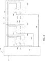
- FIG. 2 shows an example time sharing LED controller configured to control a high number of LEDs.
- Controller 200 can include an input 202.
- Input 202 can be coupled to a serial general purpose input/output (SGPIO) bus.
- SGPIO serial general purpose input/output
- Input 202 can be configured to receive via the SGPIO bus, a sequence of bits.
- the sequence of bits can include at least 3 bits of data related to an activity, locate and fail. For example, when an activity LED is to be illuminated, the bit related to activity is binary high (i.e., 1). Alternatively, when the activity LED is not to be illuminated, the bit related to activity is binary low (i.e., 0).
- the sequence of bits can also include one or more bits of data related to a selection of a drive.
- Controller 200 can also be coupled to a plurality of drives 204A, 204B, . . . 204N (collectively "204"), which can each include an activity LED 206A, 206B, . . . , 206N (collectively "206"), a locate LED 208A, 208B, . . . , 208N (collectively "208"), and a fail LED 210A, 210B, . . . , 210N (collectively "210"). Controller 200 can be coupled to activity LED 206 of each drive 204 by activity control line 212 and one of a plurality of selection lines 218A, 218B, . . . , 218N (collectively "218").
- Each selection line 218 corresponds to a specific drive 204.
- selection line 218A corresponds to drive 204A (and LEDs 206A, 208A, 210A)
- selection line 218B corresponds to drive 204B (and LEDs 206B, 208B, 210B), etc.
- controller 200 can be configured to receive a sequence of six bits from a drive controller via the SGPIO bus.
- Three of the bits e.g., most significant
- the other three bits e.g., least significant
- a sequence of bits can be 100001.
- the first three bits of the sequence i.e., 100
- activity LED 206 will be illuminated as the first bit is binary high (i.e., 1).
- the locate and fail LED will not be illuminated as the remaining bits are binary low (i.e., 0).
- the other three bits correspond to the selection of drive 204B (i.e., the second drive).
- activity LED 204B will be illuminated.
- the activity bit carrying binary high indicates activity in the drive.
- the activity bit carrying binary low indicates no activity in the drive.
- the locate bit carrying binary high indicates a user attempting to locate the drive.
- the fail bit carrying binary high indicates a failure at the drive. A drive failure can be further determined based on a pattern displayed at the fail LED.
- FIG. 3 shows a timing diagram illustrating a controller receiving sequences of bits over a period of time.
- Timing diagram 300 can be shown over a period of time 320.
- period of time 320 is eight cycles (i.e., eight sequences of bits received at the controller).
- Timing diagram 300 can represent each control line 212, 214, 216 as binary high (i.e., 1) or binary low (i.e., 0) through rows 322, 324, 326, respectively.
- Timing diagram 300 can represent selection lines 218 as binary high (i.e., 1) or binary low (i.e., 0) through rows 328, 330, 332 respectively.
- a sequence of bits is received at controller 200.
- the sequence of bits can correspond to a binary high (i.e., 1) for selection line 218A (e.g., corresponding to drive 204A), and timing diagram can show the corresponding row 328 as binary high. The remaining selection rows 330, 332 are shown as binary low. Also, during the first cycle of time, the sequence of bits is binary high (i.e., 1) for activity control line 212 and fail control line 216, and timing diagram can show corresponding rows 322 and 326 has binary high (i.e., 1). The sequence of bits is binary low (i.e., 0) for locate control line 214, and timing diagram can show corresponding row 324 as binary low.
- activity LED 206A and fail LED 210A of drive 204A will display a pattern (e.g., illuminated, flashing, different color, etc).
- FIG. 4 shows an example of cascaded configuration enabling control of an extended number of LEDs.
- a cascaded configuration includes two or more LED controllers.
- Controller 200 (previously shown in FIG. 2 ) can also include a device address input 434A.
- Device address input 434A can be configured to receive a device address (e.g., 0x0, 0x1, etc.). The device address can assign a controller a subset of drives.
- controller 200 can receive at device address input 434A a device address 0x0.
- controller 200 can be configured to control eight drives 204 in subset 436A.
- the cascaded configuration can also include controller 400.
- Controller 400 includes similar features of controller 200 (shown in FIG. 2 ). Controller 400 can also be configured to receive a device address at device address input 434N for the assignment of a subset of drives. For example, controller 400 can receive at device address input 434N, a device address 0x1. In response to receiving device address 0x1, controller 200 can be configured to control eight drives 204 in subset 436N, different from subset 436A.
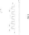
- FIG. 5 shows a timing diagram illustrating a selection of a subset of drives controlled by one of a plurality of controllers by the sequence of bits received via the SGPIO bus and a device address.
- Timing diagram 500 can be shown over a period of time 520.
- Timing diagram 500 can represent a selection of a subset of drives as binary high (i.e., 1) for each cycle (i.e., sequence of bits received through inputs 202, 402) by row 522.
- controllers 200, 400 can receive a sequence of bits at input 202, 402 via the SGPIO bus. Based on the sequence of bits and the device address received, a subset of drives can be determined.
- the first subset 436A can be determined, when controllers 200 determines, based on the received device address, that controller 200 controls the subset of drives (e.g., 436A) to which the sequence of bits pertain.
- row 522 is binary high (i.e., 1) for subset 436A.
- FIG. 6 The method shown in FIG 6 is provided by way of example, as there are a variety of ways to carry out the method. Additionally, while the example method is illustrated with a particular order of steps, those of ordinary skill in the art will appreciate that FIG. 6 and the steps illustrated therein can be executed in any order that accomplishes the technical advantages of the present disclosure and can include fewer or more steps than illustrated.
- FIG. 6 represents one or more processes, methods or subroutines, carried out in example method.
- the steps illustrated in FIG. 6 can be implemented in a system illustrated in FIG. 2 .
- the flow chart illustrated in FIG. 6 will be described in relation to and make reference to at least controller 200, as illustrated in FIG. 1 .
- Method 600 can begin at step 610.
- a controller 200 can receive at an input 202, a sequence of bits via a serial general purpose input/output bus.
- the sequence of bits can include an activity bit, a locate bit, a fail bit, and one or more selection bits.
- method 600 can proceed to step 620.
- a plurality of control lines 212, 214, 216 and one selection line of a plurality of selection lines 218 can be set based on the sequence of bits.
- the control lines and selection lines can be connected to a plurality of LEDs 206, 208, 210 connected to a plurality of drives 204.
- control line 212 can have a binary high signal
- control lines 214, 216 can have binary low signals.
- Each selection line can be assigned binary sequence (e.g., 00, 01, 10, 001, 011, etc.).
- the selection bits corresponded to one of the assigned binary sequences, the corresponding selection line can be set high. For example, when selection line 218A is assigned 00, and the selection bits are 00, selection line 218A is set binary high.
- method 600 can proceed to step 630.
- a subset of LEDs 206, 208, 210 can display a pattern based on the setting of the control lines. For example, when activity control line 212 and selection line 218A are set to binary high, LED 206A of drive 204A displays a pattern (e.g., illuminated, flashing, different color, etc.). When a subset of LEDs display a pattern, method 600 can end.
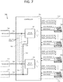
- FIG. 7 shows an example system 700 for drive management.
- a controller 702 can be implemented for managing drives (e.g., NVMe drives).
- the controller 702 can include drive registers 704, 706.
- Drive registers 704, 706 can be configured to communicate with drives 718-724 to obtain control and/or monitor drives 718-724.
- drive register 704 can be communicatively coupled with group 714 of drives, and drive register 706 can be communicatively coupled with group 716 of drives.
- Drive register 704 can obtain status information or conditions from group 714 of drives, and drive register 706 can obtain status information or conditions from group 716 of drives.
- drive register 704 can receive presence signals from group 714 of drives.
- Drive register 704 can also send control signals to group 714 of drives.
- drive register 706 can receive presence signals from group 716 of drives, and send control signals to group 716 of drives.
- Each drive register can connect to multiple drives in order to monitor and control the multiple drives, without implementing multiple input/output expander chips to support the multiple drives.
- drive register 704, 706 can connect to processors 708, 710 to relay or send status information from groups 714, 716 of drives.
- drive register 704 can connect to processor 708 via communication bus 726, and drive register 706 can connect to processor 710 via communication bus 728.
- Processor 708 can be configured to monitor and manage group 714 of drives, and processor 710 can be configured to monitor and manage group 716 of drives.
- processor 708 can communicate with drive register 704 to obtain status information about group 714 of drives, as well as send control signals to group 714 of drives.
- Processor 710 can communicate with drive register 706 to obtain status information about group 716 of drives, as well as send control signals to group 716 of drives.
- processor 708 can receive presence signals from, and send control signals to, group 714 of drives via drive register 704, and processor 710 can receive presence signals from, and send control signals to, group 716 of drives via drive register 706.
- drive register 704 can also connect to processor 710 via communication bus 734, and drive register 706 can connect to processor 708 via communication bus 736.
- processor 708 or the communication bus 726 between processor 708 and drive register 704 fails, processor 710 can communicate with drive register 704 via communication bus 734 to continue monitoring and/or management operations for group 714 of drives.
- processor 710 or communication bus 728 between processor 710 and drive register 706 fails, processor 708 can communicate with drive register 706 via communication bus 736 to continue monitoring and/or management operations for group 716 of drives.
- controller 712 can be coupled with drive registers 704, 706 to monitor and/or manage drives 718-724 in groups 714, 716 of drives.
- controller 712 can connect with drive register 704 via communication bus 732, and drive register 706 via communication bus 730.
- Controller 712 can obtain presence and status information about drives 718-724 from drive registers 704, 706, and maintain or log the status information for management and administration.
- Controller 712 can also send management signals to drive registers 704, 706 and/or processors 708, 710 to manage drives 718-724.
- controller 712 can send control signals to drive registers 704, 706 and/or processors 708, 710 to manage drives 718-724 as well as hot-plug operations.
- Controller 712 can also monitor communications from processors 708, 710 to drive registers 704, 706 to detect any communication failures.
- controller 712 can monitor communication buses 726, 728 to detect any errors or problems with communication buses 726, 728.
- controller 712 can connect to processors 708, 710 via bus 738 to monitor communications from processors 708, 710 to drive registers 704, 706 in order to detect any communication failures.
- controller 712 can provide failover of management and monitoring operations for groups 714, 716 of drives.
- processor 708 can communicate with drive register 704 via communication bus 726 to monitor and/or manage group 714 of drives. If controller 712 detects a problem with communication bus 726 and/or processor 708, controller 712 can instruct processor 710 and/or drive register 704 to share monitoring and management information about group 714 of drives via failover communication bus 734. Thus, controller 712 can switch monitoring and management of group 714 of drives from processor 708 to processor 710.
- controller 712 can instruct processor 708 and/or drive register 706 to share monitoring and management information about group 716 of drives via failover communication bus 736. Thus, controller 712 can switch monitoring and management of group 716 of drives from processor 710 to processor 708.
- Controller 712 can be a microcontroller or processor (e.g., BMC, etc.).
- communication buses 726, 728, 730, 734, 736 can be any type of communication bus, such as a serial bus (e.g., inter-integrated circuit bus, etc.).
- processors 708, 710 can be part of a same or separate computing device. For example, processors 708, 710 can reside in a single server or different servers.
- controllers, processors, drive registers, and/or drives (and groups thereof) in FIG. 7 are non-limiting examples provided for explanation purposes. One of ordinary skill in the art will recognize that other examples can include more or less controllers, processors, drive registers, drives, and/or groups of drives.
- FIG. 8 shows an example topology 800 for power control management.
- Controller 702 can communicate with latch logic circuitry 802 to provide power control management for drives 718-720.
- Latch logic circuitry 802 can store state or power information, such as presence or power status, of drives 718-720.
- the latch logic circuitry 802 can also include interfaces 824-830 (e.g., pins) for receiving power enable signals 816-818 from controller 702, and sending power enable signals 820-822 to drives 718-720.
- Controller 702 can include multifunction interfaces 808-810 for receiving presence signals from, and sending power enable signals to, drives 718-720.
- controller 702 can receive presence signal 806 from NVMe 718 at multifunction interface 808, and presence signal 804 from drive 720 at multifunction interface 810.
- Each of the multifunction interfaces 808-810 can be, for example, a multi-function pin, such as a presence and power enable pin.
- Controller 702 can determine a presence status of drives 718 and 720 based on presence signals 804-806 received at multifunction interfaces 808-810. Controller 702 can then send power enable signals 816-818 to latch logic circuitry 802 via multifunction interfaces 808-810. Latch logic circuitry 802 can receive power enable signals 816-818 via interfaces 824-826, and send power enable signals 820-822 to drives 718-720 via interfaces 828-830. Power enable signals 820-822 can power drives 718-720.
- Controller 702 can also include latch clock 812.
- Latch clock 812 can send clocked or synchronous signals 814 to latch logic circuitry 802.
- Latch logic circuitry 802 can use clocked or synchronous signals 814 for clocking, synchronizing, or timing power enable signals 820-822 to drives 718-720.
- FIG. 9 The method shown in FIG 9 is provided by way of example, as there are a variety of ways to carry out the method. Additionally, while the example method is illustrated with a particular order of steps, those of ordinary skill in the art will appreciate that FIG. 9 and the steps illustrated therein can be executed in any order that accomplishes the technical advantages of the present disclosure and can include fewer or more steps than illustrated.
- FIG. 9 represents one or more processes, methods or subroutines, carried out in example method.
- the steps illustrated in FIG. 9 can be implemented in a system illustrated in FIG. 7 .
- the flow chart illustrated in FIG. 9 will be described in relation to and make reference to at least system 700, as illustrated in FIG. 7 .
- Method 900 can begin at step 902, controller 712 can monitor bus 726 between processor 708 and drive register 704.
- Drive register 704 can be communicatively coupled with group 714 of drives, which can include drives 718-720, to send and receive status and/or control signals to and from group 714 of drives.
- Drive register 704 can send signals from group 714 of drives to processor 708, and receive signals from processor 708 and communicate those signals to specific drives in group 714 of drives.
- Processor 708 can manage (e.g., monitor, control, power, etc.) group 714 of drives by exchanging such signals with drive register 704 via bus 726.
- processor 708 can receive status information about group 714 of drives from drive register 704 via bus 726.
- Processor 708 can monitor and/or maintain status information about group 714 of drives, and send control signals or commands to specific drives in group 714 of drives.
- method 900 can proceed to step 904.
- controller 712 can detect a communication failure between processor 708 and register 704.
- the communication failure can be a failure of bus 726 and/or processor 708, which prevents communications with processor 708 through bus 726.
- the communication failure can be caused by a problem with bus 726 (e.g., a disconnection, malfunction, etc.).
- the communications failure can be a problem with processor 708.
- controller 712 can assign process 710 to manage (e.g., monitor, control, power, etc.) group 714 of drives via bus 734 and drive register 704. For example, controller 712 can switch control of monitoring operations for group 714 of drives from processor 708 to processor 710. Thus, controller 712 can enable monitoring of group 714 of drives to be taken over by processor 710 from processor 708.
- Drive register 704 can then communicate with processor 710 monitoring and/or control signals associated with drives 718-720 in group 714 of drives.
- Drive register 704 and processor 710 can communicate over bus 734, which can provide a failover path for drive register 704 to communicate presence, control, and/or power signals with processor 710 when it is unable to communicate with processor 708.
- Processor 710 can then obtain presence or status information for group 714 of drives from drive register 704, and send signals (e.g., control, power, etc.) to group 714 of drives through bus 734 and drive register 704.
- Controller 712 can also, or alternatively, detect any communications failure associated with processor 710.
- drive register 706 can be coupled with drives 722-724 in the group 716 of drives, in order to communicate status and/or control information (e.g., presence and/or control signals) with drives 722-724.
- processor 710 can communicate with drive register 706 to monitor and maintain status information about drives 722-724 in group 716.
- Processor 710 and drive register 706 can communicate such information via bus 728.
- Controller 712 can monitor processor 710 and/or bus 728 to determine if drive register 706 is able to communicate with processor 710. If drive register 706 is unable to communicate with processor 710, controller 712 can detect such communications failure and, in response, switch control of management (e.g., monitoring, controlling, etc.) operations for group 716 of drives from processor 710 to processor 708.
- switch control of management e.g., monitoring, controlling, etc.
- Controller 712 can thus enable management of group 716 of drives to be taken over by processor 708 from processor 710.
- Drive register 706 can then communicate with processor 708 for monitoring of drives 722-724 in group 716 of drives.
- Drive register 706 and processor 708 can communicate over bus 736, which can provide a failover path for drive register 706 to communicate presence, control, and/or power signals with processor 708 when it is unable to communicate with processor 710.
- Processor 708 can then obtain presence or status information for group 716 of drives from drive register 706, and send control signals to the group 716 of drives through bus 736 and drive register 706.
- controller 712 can detect communications failures between processors and drive registers.
- controller 712 detects a communications failure between a processor and a drive register that are associated with a group of drives (e.g., that are monitoring and/or managing the drives)
- controller 712 can enable the drive register to communicate with a different processor through a failover path.
- the drive register can then exchange, with the different processor through the failover path, status and/or control information for the group of drives.
- the different processor can thus communicate with the drive register, via the failover path, to monitor and/or control the group of drives.
- method 900 can end.
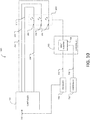
- FIG. 10 shows an example combination LED controller and drive management system 1000.
- the elements of FIG. 10 are shown in reduced capacity form in order to demonstrate combination system 1000.
- the elements of FIG. 10 are further demonstrated in previous embodiments (e.g., LED controller 200 in FIG. 2 , controller 702 and drive register 704, 706 in FIG .7 ).
- the absence or reduced capacity of an element should not suggest the element cannot and would not be included in combination system 1000 (e.g., drive register 706).
- Combination system 1000 can include LED controller 200 configured to control a high number of LEDs (206, 208, 210). Detailed operation of LED controller 200 is shown in FIG. 2 .
- Combination system 1000 can also include drive 1040 (e.g., drives 204, drives 718-724, groups 714-716 of drives, etc.). While drive 1040 is shown as a single drive with three LEDs (206, 208, 210), drive 1040 is merely representative of a plurality of disk drives (drives 204, drives 718-724, etc.) as shown in FIG. 2 and FIG. 7 .
- drive 1040 e.g., drives 204, drives 718-724, groups 714-716 of drives, etc.
- Combination system 1000 can include controller 702 for managing drive 1040.
- Controller 702 can include one or more drive registers (704, 706).
- Drive registers 704, 706 can be configured to communicate with drive 1040 to obtain control and/or monitor the drive 1040. Detailed operation of controller 702 and drive registers 704, 706 is shown in FIG. 7 .
- Combination system 1000 can include one or more processors (708, 710).
- Processors (708, 710) can obtain, from drive registers (704, 706) of controller 702 status information about drive 1040.
- the status information can include activity, locate, and fail status of drive 1040.
- processors (708, 710) can determine if (or when) the status information of drive 1040 corresponds to an activity, locate and/or fail status.
- processor (708, 710) can send a sequence of bits to input 202 of LED controller 200.
- LED controller 200 can then, as outlined in FIG. 2 , illuminate LEDs (206, 208, 210) of drive 1040 corresponding to the status information of drive 1040.
- Combination system 1000 can be best described by the following non-limiting example.
- drive 1040 can fail.
- Drive register 704 can be monitoring drive 1040.
- Drive register 704 can obtain the status information of drive 1040, which indicates drive 1040 has failed.
- controller 702 can send the status information to processor 708.
- Processor 708 can determine, based on the status information, that drive 1040 has failed.
- Processor 708 can then generate a sequence of bits. The sequence of bits can indicate drive 1040 and can also indicate a binary high for the fail bit. In some embodiments, since drive 1040 has failed and will need to be replaced, processor 708 can also indicate binary high for the locate bit.
- Processor 708 can then send the sequence of bits to input 202 of LED controller 200.
- LED controller 200 can toggle the appropriate lines (e.g., control line 218 for drive 1040, locate line 214 and fail line 216). The corresponding LEDs (locate 208, fail 210) of drive 1040 can then be illuminated.
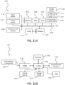
- FIG. 11A and FIG. 11B show exemplary possible system embodiments. The more appropriate embodiment will be apparent to those of ordinary skill in the art when practicing the present technology. Persons of ordinary skill in the art will also readily appreciate that other system embodiments are possible.
- FIG. 11A illustrates a conventional system bus computing system architecture 1100 wherein the components of the system are in electrical communication with each other using a bus 110.
- exemplary system 1100 includes a processing unit (CPU or processor) 1110 and a system bus 1105 that couples various system components including the system memory 1115, such as read only memory (ROM) 1120 and random access memory (RAM) 1125, to the processor 1110.
- the system 1100 can include a cache of high-speed memory connected directly with, in close proximity to, or integrated as part of the processor 1110.
- the system 1100 can copy data from the memory 1115 and/or the storage device 1130 to the cache 1112 for quick access by the processor 1110. In this way, the cache can provide a performance boost that avoids processor 1110 delays while waiting for data.
- the processor 1110 can include any general purpose processor and a hardware module or software module, such as module 1 1132, module 2 1134, and module 3 1136 stored in storage device 1130, configured to control the processor 1110 as well as a special-purpose processor where software instructions are incorporated into the actual processor design.
- the processor 1110 may essentially be a completely self-contained computing system, containing multiple cores or processors, a bus, memory controller, cache, etc.
- a multi-core processor may be symmetric or asymmetric.
- an input device 1145 can represent any number of input mechanisms, such as a microphone for speech, a touch-sensitive screen for gesture or graphical input, keyboard, mouse, motion input, speech and so forth.
- An output device 1135 can also be one or more of a number of output mechanisms known to those of skill in the art.
- multimodal systems can enable a user to provide multiple types of input to communicate with the computing device 1100.
- the communications interface 1140 can generally govern and manage the user input and system output. There is no restriction on operating on any particular hardware arrangement and therefore the basic features here may easily be substituted for improved hardware or firmware arrangements as they are developed.
- Storage device 1130 is a non-volatile memory and can be a hard disk or other types of computer readable media which can store data that are accessible by a computer, such as magnetic cassettes, flash memory cards, solid state memory devices, digital versatile disks, cartridges, random access memories (RAMs) 1125, read only memory (ROM) 1120, and hybrids thereof.
- RAMs random access memories
- ROM read only memory
- the storage device 1130 can include software modules 1132, 1134, 1136 for controlling the processor 1110. Other hardware or software modules are contemplated.
- the storage device 1130 can be connected to the system bus 1105.
- a hardware module that performs a particular function can include the software component stored in a computer-readable medium in connection with the necessary hardware components, such as the processor 1110, bus 1105, display 1135, and so forth, to carry out the function.
- FIG. 11B illustrates a computer system 1150 having a chipset architecture that can be used in executing the described method and generating and displaying a graphical user interface (GUI).
- Computer system 1150 is an example of computer hardware, software, and firmware that can be used to implement the disclosed technology.
- System 1150 can include a processor 1155, representative of any number of physically and/or logically distinct resources capable of executing software, firmware, and hardware configured to perform identified computations.
- Processor 1155 can communicate with a chipset 1160 that can control input to and output from processor 1155.
- chipset 1160 outputs information to output 1165, such as a display, and can read and write information to storage device 1170, which can include magnetic media, and solid state media, for example.
- Chipset 1160 can also read data from and write data to RAM 1175.
- a bridge 1180 for interfacing with a variety of user interface components 1185 can be provided for interfacing with chipset 1160.
- Such user interface components 1185 can include a keyboard, a microphone, touch detection and processing circuitry, a pointing device, such as a mouse, and so on.
- inputs to system 1150 can come from any of a variety of sources, machine generated and/or human generated.
- Chipset 1160 can also interface with one or more communication interfaces 1190 that can have different physical interfaces.
- Such communication interfaces can include interfaces for wired and wireless local area networks, for broadband wireless networks, as well as personal area networks.
- Some applications of the methods for generating, displaying, and using the GUI disclosed herein can include receiving ordered datasets over the physical interface or be generated by the machine itself by processor 1155 analyzing data stored in storage 1170 or 1175. Further, the machine can receive inputs from a user via user interface components 1185 and execute appropriate functions, such as browsing functions by interpreting these inputs using processor 1155.
- exemplary systems 1100 and 1150 can have more than one processor 1110 or be part of a group or cluster of computing devices networked together to provide greater processing capability.
- the present technology may be presented as including individual functional blocks including functional blocks comprising devices, device components, steps or routines in a method embodied in software, or combinations of hardware and software.
- the present technology has been described with respect to peripheral component interconnect express devices.
- the methods and concepts according to the above-described examples can be implemented for hardware recovery of other types of devices.
- the concepts described herein can be implemented for hardware recovery, including hot-add and hot-remove, of any device with hot-plug or hot-swap support, such as universal serial bus (USB) devices.
- USB universal serial bus
- peripheral component interconnect express devices are used herein as non-limiting examples for the sake of clarity and explanation purposes.
- a software module can be software that resides in memory of a client device and/or one or more servers of a content management system and perform one or more functions when a processor executes the software associated with the module.
- the memory can be a non-transitory computer-readable medium.
- the computer-readable storage devices, mediums, and memories can include a cable or wireless signal containing a bit stream and the like.
- non-transitory computer-readable storage media expressly exclude media such as energy, carrier signals, electromagnetic waves, and signals per se.
- Such instructions can comprise, for example, instructions and data which cause or otherwise configure a general purpose computer, special purpose computer, or special purpose processing device to perform a certain function or group of functions. Portions of computer resources used can be accessible over a network.
- the computer executable instructions may be, for example, binaries, intermediate format instructions such as assembly language, firmware, or source code. Examples of computer-readable media that may be used to store instructions, information used, and/or information created during methods according to described examples include magnetic or optical disks, flash memory, USB devices provided with non-volatile memory, networked storage devices, and so on.
- Devices implementing methods according to these disclosures can comprise hardware, firmware and/or software, and can take any of a variety of form factors. Typical examples of such form factors include laptops, smart phones, small form factor personal computers, personal digital assistants, and so on. Functionality described herein also can be embodied in peripherals or add-in cards. Such functionality can also be implemented on a circuit board among different chips or different processes executing in a single device, by way of further example.
- the instructions, media for conveying such instructions, computing resources for executing them, and other structures for supporting such computing resources are means for providing the functions described in these disclosures.
Landscapes
- Engineering & Computer Science (AREA)
- Theoretical Computer Science (AREA)
- General Engineering & Computer Science (AREA)
- Physics & Mathematics (AREA)
- General Physics & Mathematics (AREA)
- Human Computer Interaction (AREA)
- Quality & Reliability (AREA)
- Computer Hardware Design (AREA)
- Debugging And Monitoring (AREA)
- Hardware Redundancy (AREA)
- Information Transfer Systems (AREA)
- Techniques For Improving Reliability Of Storages (AREA)
Abstract
Description
- The subject matter herein generally relates to light emitting diodes (LED) as hard disk drive (HDD) status indicators and non-violate memory express (NVMe) drives. More specifically, the subject matter herein relates to a controller to time manage a plurality of LEDs without the need for additional LED control lines and management of topologies for drives.
- Non-volatile memory express (NVMe) is a logical device interface specification for non-volatile storage media, such as solid-state drives (SSDs), attached via the peripheral component interconnect express (PCIe) standard. NVMe technologies leverage the speed of non-volatile memory devices, such as SSDs, with the high-bandwidth bus communications supported by PCIe, to provide significant improvements in storage performance, capacity, and reliability. Not surprisingly, NVMe technologies have been implemented with increasing regularity in server and datacenter environments, to meet the higher performance demands in these deployments.
- Large deployments may include numerous NVMe drives for added capabilities. Each NVMe drive is typically assigned to a specific processor which manages and monitors that NVMe drive. A processor can be assigned to multiple NVMe drives, to manage and monitor those NVMe drives. To connect a processor with multiple NVMe drives, input/output expander chips are generally implemented, with each expander chip connecting an NVMe drive to a particular processor. Each NVMe drive assigned to a processor requires a respective input/output expander chip to connect to that processor, and each NVMe drive added requires an additional input/output expander chip. Accordingly, large deployments with numerous NVMe drives require a large number of input/output expander chips to connect the NVMe drives with respective processors. As a result, the current solutions are costly, inflexible, and cumbersome.
- Additional features and advantages of the disclosure will be set forth in the description which follows, and in part will be obvious from the description, or can be learned by practice of the herein disclosed principles. The features and advantages of the disclosure can be realized and obtained by means of the instruments and combinations particularly pointed out in the appended claims. These and other features of the disclosure will become more fully apparent from the following description and appended claims, or can be learned by the practice of the principles set forth herein.
- The approaches set forth herein can be used to efficiently manage non-volatile memory express (NVMe) drives. For example, the approaches set forth herein can provide an NVMe topology which allows multiple NVMe drives to connect to a respective processor through a register, without multiple input/output expander chips. Multiple processors can be connected to multiple registers, where each register can handle a group of NVMe drives. A controller can be connected to the drive registers to communicate with the groups of NVMe drives and the multiple processors. The controller can then manage and monitor the various groups of NVMe drives. The controller can also detect communication failures and enable a failover path for connecting a group of NVMe drives to a different processor when a current path between that group of NVMe drives and the processor fails.
- Disclosed are technologies for flexible NVMe drive management. In some examples, a system can include a first controller including a first drive register and a second drive register, a first processor communicatively coupled with the first drive register via a first bus, and a second processor communicatively coupled with the second drive register via a second bus. Moreover, the system can include a first set of NVMe drives communicatively coupled with the first processor via the first drive register, and a second set of NVMe drives communicatively coupled with the second processor via the second drive register and the second serial bus.
- The system can also include a second controller, such as a baseboard management controller (BMC), which can be communicatively coupled with the first drive register and the second drive register. The second controller can be coupled with the first drive register and the second drive register via one or more serial buses. The second controller can be configured to determine, record, and/or maintain status information about the first set of NVMe drives and the second set of NVMe drives. The second controller can communicate with the first drive register and the second drive register to determine the status of the first and second set of NVMe drives. For example, the second controller can send/receive status signals to and from the first and second drive registers. The second controller can also send control signals to the first and second drive registers, for controlling the first and second drive registers and/or the first and second set of NVMe drives.
- The first processor can be configured to communicate with the first drive register to obtain status information about the first set of NVMe drives and/or control and manage the first set of NVMe drives. Moreover, the second processor can be configured to communicate with the second drive register to obtain status information about the second set of NVMe drives and/or control and manage the second set of NVMe drives.
- The first processor can also be communicatively coupled via a serial bus with the second drive register for failover. Similarly, the second processor can be communicatively coupled via a serial bus with the first drive register for failover. The second controller can monitor the link between the first processor and the first drive register as well as the link between the second processor and the second drive register to provide a failover path in the event of a failure. For example, the second controller can detect a failure of the communication path between the first processor and the first register, and trigger the second processor to communicate with the first drive register and take over the first processor's role in managing and monitoring the first set of NVMe drives.
- The system can also include latch logic circuitry communicatively coupled with the second controller and one or more NVMe drives associated with the first set of NVMe drives or the second set of NVMe drives. For example, an NVMe drive can be coupled with the latch logic circuitry via a respective pin on the latch logic circuitry. The pin can be configured to output a respective power enable bit to the NVMe drive to power the NVMe drive. The power enable bit can be triggered in response to a presence bit transmitted by the NVMe drive to the second controller and/or the latch logic circuitry.
- The latch logic circuitry can also include a respective input pin configured to receive a power enable bit(s) from the second controller, to be transmitted to the NVMe drive to power the NVMe drive. The second controller can include a respective presence pin communicatively coupled with the respective input pin of the latch logic circuitry. The respective presence pin can be configured to function as a multifunction pin capable of receiving presence bits from the NVMe drive and sending one or more power enable bits to the respective input pin of the latch logic circuitry, to be transmitted to the NVMe drive for powering the NVMe drive.
- The above-recited and other advantages and features of the disclosure will become apparent by reference to specific embodiments thereof which are illustrated in the appended drawings. Understanding that these drawings depict only example embodiments of the disclosure and are not therefore to be considered to be limiting of its scope, the principles herein are described and explained with additional specificity and detail through the use of the accompanying drawings in which:
-
FIG 1 shows an LED controller of the prior art; -
FIG 2 shows an example LED controller for implementing various embodiments of the present technology; -
FIG. 3 shows a timing diagram of the example LED controller for implementing various embodiments of the present technology; -
FIG. 4 shows example cascaded LED controllers for implementing various embodiments of the present technology; -
FIG. 5 shows a timing diagram of the example cascaded LED controllers for implementing various embodiments of the present technology; -
FIG. 6 shows a flow chart of an example method for time sharing the example LED controller for implementing various embodiments of the present technology; -
FIG. 7 shows an example system for drive management for implementing various embodiments of the present technology; -
FIG. 8 shows an example topology for drive power control management for implementing various embodiments of the present technology; -
FIG. 9 shows a flow chart of an example method for management of non-volatile memory express drives; -
FIG. 10 shows an example combination LED controller and system for drive management for implementing various embodiments of the present technology -
FIG. 11A shows an exemplary possible system embodiment for implementing various embodiments of the present technology; and -
FIG. 11B shows an exemplary possible system embodiment for implementing various embodiments of the present technology. - Various examples of the disclosure are discussed in detail below. While specific implementations are discussed, it should be understood that this is done for illustration purposes only. A person skilled in the relevant art will recognize that other components and configurations can be used without parting from the scope of the disclosure. In other instances, well-known methods, procedures, components, circuits, and networks have not been described in detail so as not to necessarily obscure aspects of the embodiment.
- It will also be understood that, although the terms first, second, etc. can be used herein to describe various elements, these elements should not be limited by these terms. These terms are only used to distinguish one element from another. For example, a first sensor could be termed a second sensor, and similarly, a second sensor could be termed a first sensor, without departing from the scope of the present description.
- The terminology used in the description herein is for the purpose of describing particular embodiments only and is not intended to be limiting. As used in the description and the appended claims, the singular forms "a", "an" and "the" are intended to include the plural forms as well, unless the context clearly indicates otherwise. It will also be understood that the term "and/or" as used herein refers to and encompasses any and all possible combinations of one or more of the associated listed items. It will be further understood that the terms "comprises" and/or "comprising," when used in this specification, specify the presence of stated features, integers, steps, operations, elements, and/or components, but do not preclude the presence or addition of one or more other features, integers, steps, operations, elements, components, and/or groups thereof.
- As used herein, the term "if" may be construed to mean "when" or "upon" or "in response to determining" or "in response to detecting," depending on the context. Similarly, the phrase "if it is determined" or "if [a stated condition or event] is detected" may be construed to mean "upon determining" or "in response to determining" or "upon detecting [the stated condition or event]" or "in response to detecting [the stated condition or event]," depending on the context.
- As used herein, the term "drive" may be construed to mean a hard disk drive (HDD), a solid state drive (SSD), or any other type of physical hardware device used to store electronic data.
- The disclosed technology addresses the need in the art for an LED controller capable of controlling a larger number of LEDs of drives, such as a time sharing hard disk drive light emitting diode controller. Current controllers require individual control lines for each LED of each drive. New time sharing controllers require three control lines for the three LEDs (e.g., activity, locate, fail) of each drive, along with a plurality of selection lines configured to select a specific drive (and the three LEDs) per time cycle. A new time sharing controller can be configured to control a higher number of LEDs based on a reduced number of required control lines.
- The disclosed technology also addresses the need in the art for managing drives (e.g., non-volatile memory express NVMe drives, etc.). A detailed description of management of drives, including examples and variations, are described herein. These variations shall be described herein as the various embodiments are set forth.
-
FIG. 2 shows an example time sharing LED controller configured to control a high number of LEDs.Controller 200 can include aninput 202. Input 202 can be coupled to a serial general purpose input/output (SGPIO) bus. Input 202 can be configured to receive via the SGPIO bus, a sequence of bits. The sequence of bits can include at least 3 bits of data related to an activity, locate and fail. For example, when an activity LED is to be illuminated, the bit related to activity is binary high (i.e., 1). Alternatively, when the activity LED is not to be illuminated, the bit related to activity is binary low (i.e., 0). The sequence of bits can also include one or more bits of data related to a selection of a drive. The bits related to the selection of a drive can be exponentially proportional to the number of drives connected to controller 200 (i.e., 2n = x, where x is equal to the number of drives connected to the controller). For example, when four drives are connected, at least two bits must be used for selection. When eight drives are connected, at least three bits must be used for selection. -
Controller 200 can also be coupled to a plurality ofdrives activity LED LED fail LED Controller 200 can be coupled toactivity LED 206 of each drive 204 byactivity control line 212 and one of a plurality ofselection lines selection line 218 corresponds to a specific drive 204. For example,selection line 218A corresponds to drive 204A (andLEDs selection line 218B corresponds to drive 204B (andLEDs - In some examples,
controller 200 can be configured to receive a sequence of six bits from a drive controller via the SGPIO bus. Three of the bits (e.g., most significant) can be reserved for setting the threeLEDs activity LED 206 will be illuminated as the first bit is binary high (i.e., 1). The locate and fail LED will not be illuminated as the remaining bits are binary low (i.e., 0). The other three bits (i.e., 001) correspond to the selection ofdrive 204B (i.e., the second drive). Thus,activity LED 204B will be illuminated. The activity bit carrying binary high indicates activity in the drive. The activity bit carrying binary low indicates no activity in the drive. The locate bit carrying binary high indicates a user attempting to locate the drive. The fail bit carrying binary high indicates a failure at the drive. A drive failure can be further determined based on a pattern displayed at the fail LED. -
FIG. 3 shows a timing diagram illustrating a controller receiving sequences of bits over a period of time. Timing diagram 300 can be shown over a period oftime 320. In this example, period oftime 320 is eight cycles (i.e., eight sequences of bits received at the controller). Timing diagram 300 can represent eachcontrol line rows selection lines 218 as binary high (i.e., 1) or binary low (i.e., 0) throughrows controller 200. The sequence of bits can correspond to a binary high (i.e., 1) forselection line 218A (e.g., corresponding to drive 204A), and timing diagram can show thecorresponding row 328 as binary high. The remainingselection rows activity control line 212 and failcontrol line 216, and timing diagram can showcorresponding rows control line 214, and timing diagram can showcorresponding row 324 as binary low. Thus, during the first cycle of time,activity LED 206A and failLED 210A ofdrive 204A will display a pattern (e.g., illuminated, flashing, different color, etc). -
FIG. 4 shows an example of cascaded configuration enabling control of an extended number of LEDs. A cascaded configuration includes two or more LED controllers. Controller 200 (previously shown inFIG. 2 ) can also include adevice address input 434A.Device address input 434A can be configured to receive a device address (e.g., 0x0, 0x1, etc.). The device address can assign a controller a subset of drives. For example,controller 200 can receive atdevice address input 434A a device address 0x0. In response to receiving device address 0x0,controller 200 can be configured to control eight drives 204 insubset 436A. - The cascaded configuration can also include
controller 400.Controller 400 includes similar features of controller 200 (shown inFIG. 2 ).Controller 400 can also be configured to receive a device address atdevice address input 434N for the assignment of a subset of drives. For example,controller 400 can receive atdevice address input 434N, a device address 0x1. In response to receiving device address 0x1,controller 200 can be configured to control eight drives 204 insubset 436N, different fromsubset 436A. -
FIG. 5 shows a timing diagram illustrating a selection of a subset of drives controlled by one of a plurality of controllers by the sequence of bits received via the SGPIO bus and a device address. Timing diagram 500 can be shown over a period oftime 520. Timing diagram 500 can represent a selection of a subset of drives as binary high (i.e., 1) for each cycle (i.e., sequence of bits received throughinputs 202, 402) byrow 522. For example at a first cycle of time,controllers input first subset 436A can be determined, whencontrollers 200 determines, based on the received device address, thatcontroller 200 controls the subset of drives (e.g., 436A) to which the sequence of bits pertain. Thusrow 522 is binary high (i.e., 1) forsubset 436A. - The method shown in
FIG 6 is provided by way of example, as there are a variety of ways to carry out the method. Additionally, while the example method is illustrated with a particular order of steps, those of ordinary skill in the art will appreciate thatFIG. 6 and the steps illustrated therein can be executed in any order that accomplishes the technical advantages of the present disclosure and can include fewer or more steps than illustrated. - Each step shown in
FIG. 6 represents one or more processes, methods or subroutines, carried out in example method. The steps illustrated inFIG. 6 can be implemented in a system illustrated inFIG. 2 . The flow chart illustrated inFIG. 6 will be described in relation to and make reference to atleast controller 200, as illustrated inFIG. 1 . -
Method 600 can begin atstep 610. Atstep 610, acontroller 200 can receive at aninput 202, a sequence of bits via a serial general purpose input/output bus. For example, the sequence of bits can include an activity bit, a locate bit, a fail bit, and one or more selection bits. When a sequence of bits has been received,method 600 can proceed to step 620. - At
step 620, a plurality ofcontrol lines selection lines 218 can be set based on the sequence of bits. The control lines and selection lines can be connected to a plurality ofLEDs control line 212 can have a binary high signal, andcontrol lines selection line 218A is assigned 00, and the selection bits are 00,selection line 218A is set binary high. When the control lines and a selection line are set,method 600 can proceed to step 630. - At
step 630, a subset ofLEDs activity control line 212 andselection line 218A are set to binary high,LED 206A ofdrive 204A displays a pattern (e.g., illuminated, flashing, different color, etc.). When a subset of LEDs display a pattern,method 600 can end. -
FIG. 7 shows anexample system 700 for drive management. Acontroller 702 can be implemented for managing drives (e.g., NVMe drives). Thecontroller 702 can include driveregisters register 704 can be communicatively coupled withgroup 714 of drives, and driveregister 706 can be communicatively coupled withgroup 716 of drives. Driveregister 704 can obtain status information or conditions fromgroup 714 of drives, and driveregister 706 can obtain status information or conditions fromgroup 716 of drives. - For example, drive
register 704 can receive presence signals fromgroup 714 of drives. Driveregister 704 can also send control signals togroup 714 of drives. Similarly, driveregister 706 can receive presence signals fromgroup 716 of drives, and send control signals togroup 716 of drives. - Each drive register can connect to multiple drives in order to monitor and control the multiple drives, without implementing multiple input/output expander chips to support the multiple drives. Moreover, drive
register processors groups register 704 can connect toprocessor 708 viacommunication bus 726, and driveregister 706 can connect toprocessor 710 viacommunication bus 728. -
Processor 708 can be configured to monitor and managegroup 714 of drives, andprocessor 710 can be configured to monitor and managegroup 716 of drives. For example,processor 708 can communicate withdrive register 704 to obtain status information aboutgroup 714 of drives, as well as send control signals togroup 714 of drives.Processor 710 can communicate withdrive register 706 to obtain status information aboutgroup 716 of drives, as well as send control signals togroup 716 of drives. Accordingly,processor 708 can receive presence signals from, and send control signals to,group 714 of drives viadrive register 704, andprocessor 710 can receive presence signals from, and send control signals to,group 716 of drives viadrive register 706. - In order to provide failover, drive
register 704 can also connect toprocessor 710 viacommunication bus 734, and driveregister 706 can connect toprocessor 708 viacommunication bus 736. Thus, ifprocessor 708 or thecommunication bus 726 betweenprocessor 708 and driveregister 704 fails,processor 710 can communicate withdrive register 704 viacommunication bus 734 to continue monitoring and/or management operations forgroup 714 of drives. Similarly, ifprocessor 710 orcommunication bus 728 betweenprocessor 710 and driveregister 706 fails,processor 708 can communicate withdrive register 706 viacommunication bus 736 to continue monitoring and/or management operations forgroup 716 of drives. - Moreover,
controller 712 can be coupled with drive registers 704, 706 to monitor and/or manage drives 718-724 ingroups controller 712 can connect withdrive register 704 viacommunication bus 732, and driveregister 706 viacommunication bus 730.Controller 712 can obtain presence and status information about drives 718-724 from drive registers 704, 706, and maintain or log the status information for management and administration.Controller 712 can also send management signals to driveregisters processors controller 712 can send control signals to driveregisters processors -
Controller 712 can also monitor communications fromprocessors registers controller 712 can monitorcommunication buses communication buses controller 712 can connect toprocessors bus 738 to monitor communications fromprocessors registers - In response to a failure or error detected for
communication buses controller 712 can provide failover of management and monitoring operations forgroups processor 708 can communicate withdrive register 704 viacommunication bus 726 to monitor and/or managegroup 714 of drives. Ifcontroller 712 detects a problem withcommunication bus 726 and/orprocessor 708,controller 712 can instructprocessor 710 and/or driveregister 704 to share monitoring and management information aboutgroup 714 of drives viafailover communication bus 734. Thus,controller 712 can switch monitoring and management ofgroup 714 of drives fromprocessor 708 toprocessor 710. - Alternatively, if
controller 712 detects a problem withcommunication bus 728 and/orprocessor 710, it can instructprocessor 708 and/or driveregister 706 to share monitoring and management information aboutgroup 716 of drives viafailover communication bus 736. Thus,controller 712 can switch monitoring and management ofgroup 716 of drives fromprocessor 710 toprocessor 708. -
Controller 712 can be a microcontroller or processor (e.g., BMC, etc.). Moreover,communication buses processors processors - The number of controllers, processors, drive registers, and/or drives (and groups thereof) in
FIG. 7 are non-limiting examples provided for explanation purposes. One of ordinary skill in the art will recognize that other examples can include more or less controllers, processors, drive registers, drives, and/or groups of drives. -
FIG. 8 shows anexample topology 800 for power control management.Controller 702 can communicate withlatch logic circuitry 802 to provide power control management for drives 718-720.Latch logic circuitry 802 can store state or power information, such as presence or power status, of drives 718-720. Thelatch logic circuitry 802 can also include interfaces 824-830 (e.g., pins) for receiving power enable signals 816-818 fromcontroller 702, and sending power enable signals 820-822 to drives 718-720. -
Controller 702 can include multifunction interfaces 808-810 for receiving presence signals from, and sending power enable signals to, drives 718-720. For example,controller 702 can receive presence signal 806 fromNVMe 718 atmultifunction interface 808, and presence signal 804 fromdrive 720 atmultifunction interface 810. Each of the multifunction interfaces 808-810 can be, for example, a multi-function pin, such as a presence and power enable pin. -
Controller 702 can determine a presence status ofdrives Controller 702 can then send power enable signals 816-818 to latchlogic circuitry 802 via multifunction interfaces 808-810.Latch logic circuitry 802 can receive power enable signals 816-818 via interfaces 824-826, and send power enable signals 820-822 to drives 718-720 via interfaces 828-830. Power enable signals 820-822 can power drives 718-720. -
Controller 702 can also includelatch clock 812.Latch clock 812 can send clocked orsynchronous signals 814 to latchlogic circuitry 802.Latch logic circuitry 802 can use clocked orsynchronous signals 814 for clocking, synchronizing, or timing power enable signals 820-822 to drives 718-720. - The method shown in
FIG 9 is provided by way of example, as there are a variety of ways to carry out the method. Additionally, while the example method is illustrated with a particular order of steps, those of ordinary skill in the art will appreciate thatFIG. 9 and the steps illustrated therein can be executed in any order that accomplishes the technical advantages of the present disclosure and can include fewer or more steps than illustrated. - Each step shown in
FIG. 9 represents one or more processes, methods or subroutines, carried out in example method. The steps illustrated inFIG. 9 can be implemented in a system illustrated inFIG. 7 . The flow chart illustrated inFIG. 9 will be described in relation to and make reference to atleast system 700, as illustrated inFIG. 7 . -
Method 900 can begin atstep 902,controller 712 can monitorbus 726 betweenprocessor 708 and driveregister 704. Driveregister 704 can be communicatively coupled withgroup 714 of drives, which can include drives 718-720, to send and receive status and/or control signals to and fromgroup 714 of drives. Driveregister 704 can send signals fromgroup 714 of drives toprocessor 708, and receive signals fromprocessor 708 and communicate those signals to specific drives ingroup 714 of drives.Processor 708 can manage (e.g., monitor, control, power, etc.)group 714 of drives by exchanging such signals withdrive register 704 viabus 726. For example,processor 708 can receive status information aboutgroup 714 of drives fromdrive register 704 viabus 726.Processor 708 can monitor and/or maintain status information aboutgroup 714 of drives, and send control signals or commands to specific drives ingroup 714 of drives. When the controller has monitored the bus,method 900 can proceed to step 904. - At
step 904,controller 712 can detect a communication failure betweenprocessor 708 and register 704. The communication failure can be a failure ofbus 726 and/orprocessor 708, which prevents communications withprocessor 708 throughbus 726. For example, the communication failure can be caused by a problem with bus 726 (e.g., a disconnection, malfunction, etc.). As another example, the communications failure can be a problem withprocessor 708. When the controller has detected a communication failure,method 900 can proceed to step 906. - At
step 906, and in response to the communications failure,controller 712 can assignprocess 710 to manage (e.g., monitor, control, power, etc.)group 714 of drives viabus 734 and driveregister 704. For example,controller 712 can switch control of monitoring operations forgroup 714 of drives fromprocessor 708 toprocessor 710. Thus,controller 712 can enable monitoring ofgroup 714 of drives to be taken over byprocessor 710 fromprocessor 708. Driveregister 704 can then communicate withprocessor 710 monitoring and/or control signals associated with drives 718-720 ingroup 714 of drives. - Drive
register 704 andprocessor 710 can communicate overbus 734, which can provide a failover path fordrive register 704 to communicate presence, control, and/or power signals withprocessor 710 when it is unable to communicate withprocessor 708.Processor 710 can then obtain presence or status information forgroup 714 of drives fromdrive register 704, and send signals (e.g., control, power, etc.) togroup 714 of drives throughbus 734 and driveregister 704. -
Controller 712 can also, or alternatively, detect any communications failure associated withprocessor 710. For example, driveregister 706 can be coupled with drives 722-724 in thegroup 716 of drives, in order to communicate status and/or control information (e.g., presence and/or control signals) with drives 722-724. Moreover,processor 710 can communicate withdrive register 706 to monitor and maintain status information about drives 722-724 ingroup 716.Processor 710 and driveregister 706 can communicate such information viabus 728.Controller 712 can monitorprocessor 710 and/orbus 728 to determine ifdrive register 706 is able to communicate withprocessor 710. Ifdrive register 706 is unable to communicate withprocessor 710,controller 712 can detect such communications failure and, in response, switch control of management (e.g., monitoring, controlling, etc.) operations forgroup 716 of drives fromprocessor 710 toprocessor 708. -
Controller 712 can thus enable management ofgroup 716 of drives to be taken over byprocessor 708 fromprocessor 710. Driveregister 706 can then communicate withprocessor 708 for monitoring of drives 722-724 ingroup 716 of drives. Driveregister 706 andprocessor 708 can communicate overbus 736, which can provide a failover path fordrive register 706 to communicate presence, control, and/or power signals withprocessor 708 when it is unable to communicate withprocessor 710.Processor 708 can then obtain presence or status information forgroup 716 of drives fromdrive register 706, and send control signals to thegroup 716 of drives throughbus 736 and driveregister 706. - Accordingly, in a drive management system, such as
system 700,controller 712 can detect communications failures between processors and drive registers. Whencontroller 712 detects a communications failure between a processor and a drive register that are associated with a group of drives (e.g., that are monitoring and/or managing the drives),controller 712 can enable the drive register to communicate with a different processor through a failover path. The drive register can then exchange, with the different processor through the failover path, status and/or control information for the group of drives. The different processor can thus communicate with the drive register, via the failover path, to monitor and/or control the group of drives. When the controller has assigned a process to manage the group of drives,method 900 can end. -
FIG. 10 shows an example combination LED controller and drivemanagement system 1000. The elements ofFIG. 10 are shown in reduced capacity form in order to demonstratecombination system 1000. The elements ofFIG. 10 are further demonstrated in previous embodiments (e.g.,LED controller 200 inFIG. 2 ,controller 702 and driveregister FIG .7 ). The absence or reduced capacity of an element should not suggest the element cannot and would not be included in combination system 1000 (e.g., drive register 706). -
Combination system 1000 can includeLED controller 200 configured to control a high number of LEDs (206, 208, 210). Detailed operation ofLED controller 200 is shown inFIG. 2 .Combination system 1000 can also include drive 1040 (e.g., drives 204, drives 718-724, groups 714-716 of drives, etc.). Whiledrive 1040 is shown as a single drive with three LEDs (206, 208, 210),drive 1040 is merely representative of a plurality of disk drives (drives 204, drives 718-724, etc.) as shown inFIG. 2 andFIG. 7 . -
Combination system 1000 can includecontroller 702 for managingdrive 1040.Controller 702 can include one or more drive registers (704, 706). Drive registers 704, 706 can be configured to communicate withdrive 1040 to obtain control and/or monitor thedrive 1040. Detailed operation ofcontroller 702 and driveregisters FIG. 7 . -
Combination system 1000 can include one or more processors (708, 710). Processors (708, 710) can obtain, from drive registers (704, 706) ofcontroller 702 status information aboutdrive 1040. The status information can include activity, locate, and fail status ofdrive 1040. In response to receiving status information, processors (708, 710) can determine if (or when) the status information ofdrive 1040 corresponds to an activity, locate and/or fail status. When processor (708, 710) determines the status information corresponds to an activity, locate and/or fail status ofdrive 1040, processor (708, 710) can send a sequence of bits to input 202 ofLED controller 200.LED controller 200 can then, as outlined inFIG. 2 , illuminate LEDs (206, 208, 210) ofdrive 1040 corresponding to the status information ofdrive 1040. -
Combination system 1000 can be best described by the following non-limiting example. In this example, drive 1040 can fail. Driveregister 704 can be monitoringdrive 1040. Driveregister 704 can obtain the status information ofdrive 1040, which indicatesdrive 1040 has failed. In response to obtaining the status information indicating a failure ofdrive 1040,controller 702 can send the status information toprocessor 708.Processor 708 can determine, based on the status information, that drive 1040 has failed.Processor 708 can then generate a sequence of bits. The sequence of bits can indicate drive 1040 and can also indicate a binary high for the fail bit. In some embodiments, sincedrive 1040 has failed and will need to be replaced,processor 708 can also indicate binary high for the locate bit.Processor 708 can then send the sequence of bits to input 202 ofLED controller 200. In response to receiving the sequence of bits,LED controller 200 can toggle the appropriate lines (e.g.,control line 218 fordrive 1040, locateline 214 and fail line 216). The corresponding LEDs (locate 208, fail 210) ofdrive 1040 can then be illuminated. -
FIG. 11A and FIG. 11B show exemplary possible system embodiments. The more appropriate embodiment will be apparent to those of ordinary skill in the art when practicing the present technology. Persons of ordinary skill in the art will also readily appreciate that other system embodiments are possible. -
FIG. 11A illustrates a conventional system buscomputing system architecture 1100 wherein the components of the system are in electrical communication with each other using a bus 110.Exemplary system 1100 includes a processing unit (CPU or processor) 1110 and asystem bus 1105 that couples various system components including thesystem memory 1115, such as read only memory (ROM) 1120 and random access memory (RAM) 1125, to theprocessor 1110. Thesystem 1100 can include a cache of high-speed memory connected directly with, in close proximity to, or integrated as part of theprocessor 1110. Thesystem 1100 can copy data from thememory 1115 and/or thestorage device 1130 to thecache 1112 for quick access by theprocessor 1110. In this way, the cache can provide a performance boost that avoidsprocessor 1110 delays while waiting for data. These and other modules can control or be configured to control theprocessor 1110 to perform various actions.Other system memory 1115 may be available for use as well. Thememory 1115 can include multiple different types of memory with different performance characteristics. Theprocessor 1110 can include any general purpose processor and a hardware module or software module, such asmodule 1 1132,module 2 1134, andmodule 3 1136 stored instorage device 1130, configured to control theprocessor 1110 as well as a special-purpose processor where software instructions are incorporated into the actual processor design. Theprocessor 1110 may essentially be a completely self-contained computing system, containing multiple cores or processors, a bus, memory controller, cache, etc. A multi-core processor may be symmetric or asymmetric. - To enable user interaction with the
computing device 1100, aninput device 1145 can represent any number of input mechanisms, such as a microphone for speech, a touch-sensitive screen for gesture or graphical input, keyboard, mouse, motion input, speech and so forth. Anoutput device 1135 can also be one or more of a number of output mechanisms known to those of skill in the art. In some instances, multimodal systems can enable a user to provide multiple types of input to communicate with thecomputing device 1100. Thecommunications interface 1140 can generally govern and manage the user input and system output. There is no restriction on operating on any particular hardware arrangement and therefore the basic features here may easily be substituted for improved hardware or firmware arrangements as they are developed. -
Storage device 1130 is a non-volatile memory and can be a hard disk or other types of computer readable media which can store data that are accessible by a computer, such as magnetic cassettes, flash memory cards, solid state memory devices, digital versatile disks, cartridges, random access memories (RAMs) 1125, read only memory (ROM) 1120, and hybrids thereof. - The
storage device 1130 can includesoftware modules processor 1110. Other hardware or software modules are contemplated. Thestorage device 1130 can be connected to thesystem bus 1105. In one aspect, a hardware module that performs a particular function can include the software component stored in a computer-readable medium in connection with the necessary hardware components, such as theprocessor 1110,bus 1105,display 1135, and so forth, to carry out the function. -
FIG. 11B illustrates acomputer system 1150 having a chipset architecture that can be used in executing the described method and generating and displaying a graphical user interface (GUI).Computer system 1150 is an example of computer hardware, software, and firmware that can be used to implement the disclosed technology.System 1150 can include a processor 1155, representative of any number of physically and/or logically distinct resources capable of executing software, firmware, and hardware configured to perform identified computations. Processor 1155 can communicate with achipset 1160 that can control input to and output from processor 1155. In this example,chipset 1160 outputs information tooutput 1165, such as a display, and can read and write information tostorage device 1170, which can include magnetic media, and solid state media, for example.Chipset 1160 can also read data from and write data toRAM 1175. Abridge 1180 for interfacing with a variety ofuser interface components 1185 can be provided for interfacing withchipset 1160. Suchuser interface components 1185 can include a keyboard, a microphone, touch detection and processing circuitry, a pointing device, such as a mouse, and so on. In general, inputs tosystem 1150 can come from any of a variety of sources, machine generated and/or human generated. -
Chipset 1160 can also interface with one ormore communication interfaces 1190 that can have different physical interfaces. Such communication interfaces can include interfaces for wired and wireless local area networks, for broadband wireless networks, as well as personal area networks. Some applications of the methods for generating, displaying, and using the GUI disclosed herein can include receiving ordered datasets over the physical interface or be generated by the machine itself by processor 1155 analyzing data stored instorage user interface components 1185 and execute appropriate functions, such as browsing functions by interpreting these inputs using processor 1155. - It can be appreciated that
exemplary systems processor 1110 or be part of a group or cluster of computing devices networked together to provide greater processing capability. - For clarity of explanation, in some instances the present technology may be presented as including individual functional blocks including functional blocks comprising devices, device components, steps or routines in a method embodied in software, or combinations of hardware and software. In some instances, the present technology has been described with respect to peripheral component interconnect express devices. However, the methods and concepts according to the above-described examples can be implemented for hardware recovery of other types of devices. Indeed, the concepts described herein can be implemented for hardware recovery, including hot-add and hot-remove, of any device with hot-plug or hot-swap support, such as universal serial bus (USB) devices. Again, peripheral component interconnect express devices are used herein as non-limiting examples for the sake of clarity and explanation purposes.
- Any of the steps, operations, functions, or processes described herein may be performed or implemented by a combination of hardware and software modules, alone or in combination with other devices. In an embodiment, a software module can be software that resides in memory of a client device and/or one or more servers of a content management system and perform one or more functions when a processor executes the software associated with the module. The memory can be a non-transitory computer-readable medium.
- In some embodiments the computer-readable storage devices, mediums, and memories can include a cable or wireless signal containing a bit stream and the like. However, when mentioned, non-transitory computer-readable storage media expressly exclude media such as energy, carrier signals, electromagnetic waves, and signals per se.
- Methods according to the above-described examples can be implemented using computer-executable instructions that are stored or otherwise available from computer readable media. Such instructions can comprise, for example, instructions and data which cause or otherwise configure a general purpose computer, special purpose computer, or special purpose processing device to perform a certain function or group of functions. Portions of computer resources used can be accessible over a network. The computer executable instructions may be, for example, binaries, intermediate format instructions such as assembly language, firmware, or source code. Examples of computer-readable media that may be used to store instructions, information used, and/or information created during methods according to described examples include magnetic or optical disks, flash memory, USB devices provided with non-volatile memory, networked storage devices, and so on.
- Devices implementing methods according to these disclosures can comprise hardware, firmware and/or software, and can take any of a variety of form factors. Typical examples of such form factors include laptops, smart phones, small form factor personal computers, personal digital assistants, and so on. Functionality described herein also can be embodied in peripherals or add-in cards. Such functionality can also be implemented on a circuit board among different chips or different processes executing in a single device, by way of further example.
- The instructions, media for conveying such instructions, computing resources for executing them, and other structures for supporting such computing resources are means for providing the functions described in these disclosures.
- Although a variety of examples and other information was used to explain aspects within the scope of the appended claims, no limitation of the claims should be implied based on particular features or arrangements in such examples, as one of ordinary skill would be able to use these examples to derive a wide variety of implementations. Further and although some subject matter may have been described in language specific to examples of structural features and/or method steps, it is to be understood that the subject matter defined in the appended claims is not necessarily limited to these described features or acts. For example, such functionality can be distributed differently or performed in components other than those identified herein. Rather, the described features and steps are disclosed as examples of components of systems and methods within the scope of the appended claims.
Claims (13)
- A system comprising:a first controller comprising a first drive register and a second drive register;a first processor communicatively coupled with the first drive register via a first serial bus;a second processor communicatively coupled with the second drive register via a second serial bus;a first set of non-volatile memory express drives communicatively coupled with the first processor via the first drive register and the first serial bus; anda second set of non-volatile memory express drives communicatively coupled with the second processor via the second drive register and the second serial bus.
- The system of claim 1, further comprising:a second controller communicatively coupled with the first drive register via a third serial bus, and the second drive register respectively via a fourth serial bus.
- The system of claim 2, wherein the second controller is configured to determine and maintain status conditions of the first set of non-volatile memory express drives and the second set of non-volatile memory express drives.
- The system of claim 3, wherein the second controller is configured to determine the status conditions based on one or more drive signals received by the first drive register or the second drive register.
- The system of any of claims 2 to 4, wherein the first processor is further communicatively coupled with the second drive register via a fifth serial bus and the second processor is further communicatively coupled with the first drive register via a sixth serial bus.
- The system of claim 5, wherein the first processor is configured to monitor the first set of non-volatile memory express drives based on one or more signals received from the first set of non-volatile memory express drives through the first drive register, and wherein the second processor is configured to monitor the second set of non-volatile memory express drives based on one or more signals received from the second set of non-volatile memory express drives through the second drive register.
- The system of claim 6, wherein
the second controller is configured to detect a communication failure between the first processor and the first drive register and, in response to the communication failure, establish a communication path between the first set of non-volatile memory express drives and the second processor through the sixth serial bus, for monitoring the first set of non-volatile memory express drives via the second processor,
the second controller is configured to detect when a new non-volatile memory express drive is connected to, and disconnected from, the first drive register or the second drive register, and/or
the second controller comprises a baseboard management controller, and wherein the first serial bus, the second serial bus, the third serial bus, the fourth serial bus, the fifth serial bus, and the sixth serial bus comprise inter-integrated circuit buses. - The system of any of the previous claims, further comprising:a second controller communicatively coupled with the first drive register and the second drive register via a third serial bus;latch logic circuitry communicatively coupled with the second controller and one or more non-volatile memory express drives associated with the first set of non-volatile memory express drives or the second set of non-volatile memory express drives.
- The system of claim 8, wherein each respective one of the one or more non-volatile memory express drives is coupled with the latch logic circuitry via a respective output pin configured to output a respective power enable bit to the respective one of the one or more non-volatile memory express drives in response to a presence bit transmitted by the respective one of the one or more non-volatile memory express drives to at least one of the second controller and the latch logic circuitry.
- The system of claim 9, wherein the latch logic circuitry comprises a respective input pin configured to receive the respective power enable bit from the second controller, wherein the second controller comprises a respective presence pin communicatively coupled with the respective input pin associated with the latch logic circuitry.
- The system of claim 10, wherein the respective presence pin is configured to function as a multifunction pin capable of receiving presence bits from the respective one of the non-volatile memory express drives and sending the respective power enable bit to the respective input pin for powering the respective one of the non-volatile memory express drives.
- A method comprising:monitoring, via a first controller, a first communication path between a first processor and a first drive register on a second controller, wherein the first drive register is communicatively coupled with a plurality of non-volatile memory express drives, and wherein the first processor is configured to obtain status information about the plurality of non-volatile memory express drives from the first drive register via the first communication path;detecting, by the first controller, a communication failure of the first communication path; andin response to the communication failure, assigning, by the first controller, a second processor to receive the status information about the plurality of non-volatile memory express drives from the first drive register via a second communication path between the second processor and the first drive register.
- The method of claim 12, wherein the second controller comprises a second drive register coupled with a second plurality of non-volatile memory express drives, wherein the second drive register is configured to communicate, with at least one of the first controller and the second processor, status signals associated with the second plurality of non-volatile memory express drives.
Applications Claiming Priority (1)
| Application Number | Priority Date | Filing Date | Title |
|---|---|---|---|
| US15/153,014 US10019402B2 (en) | 2016-05-12 | 2016-05-12 | Flexible NVME drive management solution via multiple processor and registers without multiple input/output expander chips |
Publications (2)
| Publication Number | Publication Date |
|---|---|
| EP3244319A1 true EP3244319A1 (en) | 2017-11-15 |
| EP3244319B1 EP3244319B1 (en) | 2021-07-07 |
Family
ID=58992613
Family Applications (1)
| Application Number | Title | Priority Date | Filing Date |
|---|---|---|---|
| EP17170680.7A Active EP3244319B1 (en) | 2016-05-12 | 2017-05-11 | Flexible nvme drive management solution |
Country Status (5)
| Country | Link |
|---|---|
| US (1) | US10019402B2 (en) |
| EP (1) | EP3244319B1 (en) |
| JP (1) | JP6549632B2 (en) |
| CN (1) | CN107368401B (en) |
| TW (1) | TWI587134B (en) |
Families Citing this family (9)
| Publication number | Priority date | Publication date | Assignee | Title |
|---|---|---|---|---|
| CN107729220B (en) * | 2017-09-27 | 2019-06-18 | 郑州云海信息技术有限公司 | A design method for realizing multi-NVMe hard disk backplane lighting |
| CN107870844A (en) * | 2017-10-16 | 2018-04-03 | 鸿富锦精密电子(天津)有限公司 | Disk state arrangement for detecting and method |
| TWI665554B (en) | 2018-01-22 | 2019-07-11 | 緯穎科技服務股份有限公司 | Hot swap control circuit and related storage server system |
| CN109062771A (en) * | 2018-07-11 | 2018-12-21 | 郑州云海信息技术有限公司 | A kind of server monitoring OLED module redundancy approach, device, equipment and storage medium |
| US10795846B1 (en) * | 2019-07-15 | 2020-10-06 | Cisco Technology, Inc. | Scalable NVMe storage management over system management bus |
| US20230030168A1 (en) * | 2021-07-27 | 2023-02-02 | Dell Products L.P. | Protection of i/o paths against network partitioning and component failures in nvme-of environments |
| US12130755B2 (en) * | 2021-09-07 | 2024-10-29 | Micron Technology, Inc. | Serial interface for an active input/output expander of a memory sub-system |
| US12185492B2 (en) * | 2022-05-26 | 2024-12-31 | Softiron Limited | Electrostatic caddy indicator |
| US20240232662A9 (en) * | 2022-10-21 | 2024-07-11 | Dell Products L.P. | Component health determination and reporting system |
Citations (3)
| Publication number | Priority date | Publication date | Assignee | Title |
|---|---|---|---|---|
| US20070079032A1 (en) * | 2005-09-30 | 2007-04-05 | Intel Corporation | Serial signal ordering in serial general purpose input output (SGPIO) |
| US8078770B1 (en) * | 2007-08-10 | 2011-12-13 | American Megatrends, Inc. | Combining multiple SGPIO streams to provide device status indicators |
| WO2015200313A1 (en) * | 2014-06-23 | 2015-12-30 | Liqid Inc. | Modular switched fabric for data storage systems |
Family Cites Families (11)
| Publication number | Priority date | Publication date | Assignee | Title |
|---|---|---|---|---|
| JPH04249263A (en) * | 1991-02-06 | 1992-09-04 | Fuji Xerox Co Ltd | Recorded information collecting system for recording device control system |
| US7006402B2 (en) * | 2003-08-29 | 2006-02-28 | Hynix Semiconductor Inc | Multi-port memory device |
| KR100655081B1 (en) * | 2005-12-22 | 2006-12-08 | 삼성전자주식회사 | Multi-port semiconductor memory device having variable access path and method thereof |
| US8769213B2 (en) | 2009-08-24 | 2014-07-01 | Micron Technology, Inc. | Multi-port memory and operation |
| JP5569074B2 (en) * | 2010-03-19 | 2014-08-13 | 日本電気株式会社 | Storage system |
| US10121528B2 (en) * | 2012-11-30 | 2018-11-06 | Intel Corporation | Apparatus, method and system for providing termination for multiple chips of an integrated circuit package |
| JP2015114873A (en) * | 2013-12-12 | 2015-06-22 | 富士通株式会社 | Information processing apparatus and monitoring method |
| WO2015162660A1 (en) * | 2014-04-21 | 2015-10-29 | 株式会社日立製作所 | Computer system |
| US9933976B2 (en) * | 2014-04-28 | 2018-04-03 | Hitachi, Ltd. | Storage apparatus and data processing method thereof, and storage system |
| US9645902B2 (en) * | 2014-06-23 | 2017-05-09 | Liqid Inc. | Modular switched fabric for data storage systems |
| KR102309798B1 (en) * | 2015-04-16 | 2021-10-06 | 삼성전자주식회사 | SR-IOV based non volatile memory controller and method for dynamically allocating resources to queues by the non volatile memory controller |
-
2016
- 2016-05-12 US US15/153,014 patent/US10019402B2/en active Active
- 2016-09-10 TW TW105129448A patent/TWI587134B/en active
- 2016-09-27 CN CN201610852496.4A patent/CN107368401B/en active Active
-
2017
- 2017-04-18 JP JP2017081734A patent/JP6549632B2/en active Active
- 2017-05-11 EP EP17170680.7A patent/EP3244319B1/en active Active
Patent Citations (3)
| Publication number | Priority date | Publication date | Assignee | Title |
|---|---|---|---|---|
| US20070079032A1 (en) * | 2005-09-30 | 2007-04-05 | Intel Corporation | Serial signal ordering in serial general purpose input output (SGPIO) |
| US8078770B1 (en) * | 2007-08-10 | 2011-12-13 | American Megatrends, Inc. | Combining multiple SGPIO streams to provide device status indicators |
| WO2015200313A1 (en) * | 2014-06-23 | 2015-12-30 | Liqid Inc. | Modular switched fabric for data storage systems |
Also Published As
| Publication number | Publication date |
|---|---|
| CN107368401B (en) | 2020-12-25 |
| CN107368401A (en) | 2017-11-21 |
| US20170329736A1 (en) | 2017-11-16 |
| US10019402B2 (en) | 2018-07-10 |
| TWI587134B (en) | 2017-06-11 |
| JP2017204269A (en) | 2017-11-16 |
| JP6549632B2 (en) | 2019-07-24 |
| TW201810043A (en) | 2018-03-16 |
| EP3244319B1 (en) | 2021-07-07 |
Similar Documents
| Publication | Publication Date | Title |
|---|---|---|
| EP3244319B1 (en) | Flexible nvme drive management solution | |
| US9965367B2 (en) | Automatic hardware recovery system | |
| CN106649048B (en) | Indicator light control system and light emitting diode control method | |
| TWI556113B (en) | Hot-pluggable computing system, computer-implemented method and system | |
| US9858161B2 (en) | Implementing cable failover in multiple cable PCI express IO interconnections | |
| EP3540605A1 (en) | Cpld cache application in a multi-master topology system | |
| US10846159B2 (en) | System and method for managing, resetting and diagnosing failures of a device management bus | |
| US9164861B2 (en) | Drive mapping using a plurality of connected enclosure management controllers | |
| CN106155970B (en) | automatic hardware recovery method and automatic hardware recovery system | |
| US20170371814A1 (en) | Nvme drive detection from a sas/sata connector | |
| US11640377B2 (en) | Event-based generation of context-aware telemetry reports | |
| US10783109B2 (en) | Device management messaging protocol proxy | |
| US11308002B2 (en) | Systems and methods for detecting expected user intervention across multiple blades during a keyboard, video, and mouse (KVM) session | |
| CN115757236B (en) | A storage expansion pooling device and system | |
| CN118643000B (en) | Method for generating configuration information table of PCIe port of server, method and device for sending configuration information table | |
| US10853211B2 (en) | System and method for chassis-based virtual storage drive configuration | |
| US20210226876A1 (en) | Systems and methods for extended support of deprecated products | |
| TWI659302B (en) | Hdd monitoring system | |
| US11782810B2 (en) | Systems and methods for automated field replacement component configuration | |
| US20160320993A1 (en) | Control apparatus and storage system | |
| US11836127B2 (en) | Unique identification of metric values in telemetry reports | |
| US10853547B2 (en) | System and method to identify critical FPGA card sensors | |
| US10409940B1 (en) | System and method to proxy networking statistics for FPGA cards | |
| CN110321263B (en) | Hard disk monitoring system | |
| US20250068553A1 (en) | Cpld as adapter for high-availability drive management |
Legal Events
| Date | Code | Title | Description |
|---|---|---|---|
| PUAI | Public reference made under article 153(3) epc to a published international application that has entered the european phase |
Free format text: ORIGINAL CODE: 0009012 |
|
| STAA | Information on the status of an ep patent application or granted ep patent |
Free format text: STATUS: THE APPLICATION HAS BEEN PUBLISHED |
|
| AK | Designated contracting states |
Kind code of ref document: A1 Designated state(s): AL AT BE BG CH CY CZ DE DK EE ES FI FR GB GR HR HU IE IS IT LI LT LU LV MC MK MT NL NO PL PT RO RS SE SI SK SM TR |
|
| AX | Request for extension of the european patent |
Extension state: BA ME |
|
| STAA | Information on the status of an ep patent application or granted ep patent |
Free format text: STATUS: REQUEST FOR EXAMINATION WAS MADE |
|
| 17P | Request for examination filed |
Effective date: 20180515 |
|
| RBV | Designated contracting states (corrected) |
Designated state(s): AL AT BE BG CH CY CZ DE DK EE ES FI FR GB GR HR HU IE IS IT LI LT LU LV MC MK MT NL NO PL PT RO RS SE SI SK SM TR |
|
| STAA | Information on the status of an ep patent application or granted ep patent |
Free format text: STATUS: EXAMINATION IS IN PROGRESS |
|
| 17Q | First examination report despatched |
Effective date: 20191108 |
|
| GRAP | Despatch of communication of intention to grant a patent |
Free format text: ORIGINAL CODE: EPIDOSNIGR1 |
|
| STAA | Information on the status of an ep patent application or granted ep patent |
Free format text: STATUS: GRANT OF PATENT IS INTENDED |
|
| INTG | Intention to grant announced |
Effective date: 20210218 |
|
| GRAS | Grant fee paid |
Free format text: ORIGINAL CODE: EPIDOSNIGR3 |
|
| GRAA | (expected) grant |
Free format text: ORIGINAL CODE: 0009210 |
|
| STAA | Information on the status of an ep patent application or granted ep patent |
Free format text: STATUS: THE PATENT HAS BEEN GRANTED |
|
| AK | Designated contracting states |
Kind code of ref document: B1 Designated state(s): AL AT BE BG CH CY CZ DE DK EE ES FI FR GB GR HR HU IE IS IT LI LT LU LV MC MK MT NL NO PL PT RO RS SE SI SK SM TR |
|
| REG | Reference to a national code |
Ref country code: GB Ref legal event code: FG4D |
|
| REG | Reference to a national code |
Ref country code: AT Ref legal event code: REF Ref document number: 1409259 Country of ref document: AT Kind code of ref document: T Effective date: 20210715 |
|
| REG | Reference to a national code |
Ref country code: DE Ref legal event code: R096 Ref document number: 602017041521 Country of ref document: DE |
|
| REG | Reference to a national code |
Ref country code: IE Ref legal event code: FG4D |
|
| REG | Reference to a national code |
Ref country code: LT Ref legal event code: MG9D |
|
| REG | Reference to a national code |
Ref country code: NL Ref legal event code: MP Effective date: 20210707 |
|
| REG | Reference to a national code |
Ref country code: AT Ref legal event code: MK05 Ref document number: 1409259 Country of ref document: AT Kind code of ref document: T Effective date: 20210707 |
|
| PG25 | Lapsed in a contracting state [announced via postgrant information from national office to epo] |
Ref country code: LT Free format text: LAPSE BECAUSE OF FAILURE TO SUBMIT A TRANSLATION OF THE DESCRIPTION OR TO PAY THE FEE WITHIN THE PRESCRIBED TIME-LIMIT Effective date: 20210707 Ref country code: AT Free format text: LAPSE BECAUSE OF FAILURE TO SUBMIT A TRANSLATION OF THE DESCRIPTION OR TO PAY THE FEE WITHIN THE PRESCRIBED TIME-LIMIT Effective date: 20210707 Ref country code: BG Free format text: LAPSE BECAUSE OF FAILURE TO SUBMIT A TRANSLATION OF THE DESCRIPTION OR TO PAY THE FEE WITHIN THE PRESCRIBED TIME-LIMIT Effective date: 20211007 Ref country code: HR Free format text: LAPSE BECAUSE OF FAILURE TO SUBMIT A TRANSLATION OF THE DESCRIPTION OR TO PAY THE FEE WITHIN THE PRESCRIBED TIME-LIMIT Effective date: 20210707 Ref country code: ES Free format text: LAPSE BECAUSE OF FAILURE TO SUBMIT A TRANSLATION OF THE DESCRIPTION OR TO PAY THE FEE WITHIN THE PRESCRIBED TIME-LIMIT Effective date: 20210707 Ref country code: FI Free format text: LAPSE BECAUSE OF FAILURE TO SUBMIT A TRANSLATION OF THE DESCRIPTION OR TO PAY THE FEE WITHIN THE PRESCRIBED TIME-LIMIT Effective date: 20210707 Ref country code: NO Free format text: LAPSE BECAUSE OF FAILURE TO SUBMIT A TRANSLATION OF THE DESCRIPTION OR TO PAY THE FEE WITHIN THE PRESCRIBED TIME-LIMIT Effective date: 20211007 Ref country code: NL Free format text: LAPSE BECAUSE OF FAILURE TO SUBMIT A TRANSLATION OF THE DESCRIPTION OR TO PAY THE FEE WITHIN THE PRESCRIBED TIME-LIMIT Effective date: 20210707 Ref country code: PT Free format text: LAPSE BECAUSE OF FAILURE TO SUBMIT A TRANSLATION OF THE DESCRIPTION OR TO PAY THE FEE WITHIN THE PRESCRIBED TIME-LIMIT Effective date: 20211108 Ref country code: RS Free format text: LAPSE BECAUSE OF FAILURE TO SUBMIT A TRANSLATION OF THE DESCRIPTION OR TO PAY THE FEE WITHIN THE PRESCRIBED TIME-LIMIT Effective date: 20210707 Ref country code: SE Free format text: LAPSE BECAUSE OF FAILURE TO SUBMIT A TRANSLATION OF THE DESCRIPTION OR TO PAY THE FEE WITHIN THE PRESCRIBED TIME-LIMIT Effective date: 20210707 |
|
| PG25 | Lapsed in a contracting state [announced via postgrant information from national office to epo] |
Ref country code: PL Free format text: LAPSE BECAUSE OF FAILURE TO SUBMIT A TRANSLATION OF THE DESCRIPTION OR TO PAY THE FEE WITHIN THE PRESCRIBED TIME-LIMIT Effective date: 20210707 Ref country code: LV Free format text: LAPSE BECAUSE OF FAILURE TO SUBMIT A TRANSLATION OF THE DESCRIPTION OR TO PAY THE FEE WITHIN THE PRESCRIBED TIME-LIMIT Effective date: 20210707 Ref country code: GR Free format text: LAPSE BECAUSE OF FAILURE TO SUBMIT A TRANSLATION OF THE DESCRIPTION OR TO PAY THE FEE WITHIN THE PRESCRIBED TIME-LIMIT Effective date: 20211008 |
|
| REG | Reference to a national code |
Ref country code: DE Ref legal event code: R097 Ref document number: 602017041521 Country of ref document: DE |
|
| PG25 | Lapsed in a contracting state [announced via postgrant information from national office to epo] |
Ref country code: DK Free format text: LAPSE BECAUSE OF FAILURE TO SUBMIT A TRANSLATION OF THE DESCRIPTION OR TO PAY THE FEE WITHIN THE PRESCRIBED TIME-LIMIT Effective date: 20210707 |
|
| PLBE | No opposition filed within time limit |
Free format text: ORIGINAL CODE: 0009261 |
|
| STAA | Information on the status of an ep patent application or granted ep patent |
Free format text: STATUS: NO OPPOSITION FILED WITHIN TIME LIMIT |
|
| PG25 | Lapsed in a contracting state [announced via postgrant information from national office to epo] |
Ref country code: SM Free format text: LAPSE BECAUSE OF FAILURE TO SUBMIT A TRANSLATION OF THE DESCRIPTION OR TO PAY THE FEE WITHIN THE PRESCRIBED TIME-LIMIT Effective date: 20210707 Ref country code: SK Free format text: LAPSE BECAUSE OF FAILURE TO SUBMIT A TRANSLATION OF THE DESCRIPTION OR TO PAY THE FEE WITHIN THE PRESCRIBED TIME-LIMIT Effective date: 20210707 Ref country code: RO Free format text: LAPSE BECAUSE OF FAILURE TO SUBMIT A TRANSLATION OF THE DESCRIPTION OR TO PAY THE FEE WITHIN THE PRESCRIBED TIME-LIMIT Effective date: 20210707 Ref country code: EE Free format text: LAPSE BECAUSE OF FAILURE TO SUBMIT A TRANSLATION OF THE DESCRIPTION OR TO PAY THE FEE WITHIN THE PRESCRIBED TIME-LIMIT Effective date: 20210707 Ref country code: CZ Free format text: LAPSE BECAUSE OF FAILURE TO SUBMIT A TRANSLATION OF THE DESCRIPTION OR TO PAY THE FEE WITHIN THE PRESCRIBED TIME-LIMIT Effective date: 20210707 Ref country code: AL Free format text: LAPSE BECAUSE OF FAILURE TO SUBMIT A TRANSLATION OF THE DESCRIPTION OR TO PAY THE FEE WITHIN THE PRESCRIBED TIME-LIMIT Effective date: 20210707 |
|
| 26N | No opposition filed |
Effective date: 20220408 |
|
| PG25 | Lapsed in a contracting state [announced via postgrant information from national office to epo] |
Ref country code: IT Free format text: LAPSE BECAUSE OF FAILURE TO SUBMIT A TRANSLATION OF THE DESCRIPTION OR TO PAY THE FEE WITHIN THE PRESCRIBED TIME-LIMIT Effective date: 20210707 |
|
| REG | Reference to a national code |
Ref country code: CH Ref legal event code: PL |
|
| REG | Reference to a national code |
Ref country code: BE Ref legal event code: MM Effective date: 20220531 |
|
| PG25 | Lapsed in a contracting state [announced via postgrant information from national office to epo] |
Ref country code: MC Free format text: LAPSE BECAUSE OF FAILURE TO SUBMIT A TRANSLATION OF THE DESCRIPTION OR TO PAY THE FEE WITHIN THE PRESCRIBED TIME-LIMIT Effective date: 20210707 Ref country code: LU Free format text: LAPSE BECAUSE OF NON-PAYMENT OF DUE FEES Effective date: 20220511 Ref country code: LI Free format text: LAPSE BECAUSE OF NON-PAYMENT OF DUE FEES Effective date: 20220531 Ref country code: CH Free format text: LAPSE BECAUSE OF NON-PAYMENT OF DUE FEES Effective date: 20220531 |
|
| PG25 | Lapsed in a contracting state [announced via postgrant information from national office to epo] |
Ref country code: IE Free format text: LAPSE BECAUSE OF NON-PAYMENT OF DUE FEES Effective date: 20220511 |
|
| PG25 | Lapsed in a contracting state [announced via postgrant information from national office to epo] |
Ref country code: BE Free format text: LAPSE BECAUSE OF NON-PAYMENT OF DUE FEES Effective date: 20220531 |
|
| PG25 | Lapsed in a contracting state [announced via postgrant information from national office to epo] |
Ref country code: HU Free format text: LAPSE BECAUSE OF FAILURE TO SUBMIT A TRANSLATION OF THE DESCRIPTION OR TO PAY THE FEE WITHIN THE PRESCRIBED TIME-LIMIT; INVALID AB INITIO Effective date: 20170511 |
|
| PG25 | Lapsed in a contracting state [announced via postgrant information from national office to epo] |
Ref country code: MK Free format text: LAPSE BECAUSE OF FAILURE TO SUBMIT A TRANSLATION OF THE DESCRIPTION OR TO PAY THE FEE WITHIN THE PRESCRIBED TIME-LIMIT Effective date: 20210707 Ref country code: CY Free format text: LAPSE BECAUSE OF FAILURE TO SUBMIT A TRANSLATION OF THE DESCRIPTION OR TO PAY THE FEE WITHIN THE PRESCRIBED TIME-LIMIT Effective date: 20210707 |
|
| PG25 | Lapsed in a contracting state [announced via postgrant information from national office to epo] |
Ref country code: TR Free format text: LAPSE BECAUSE OF FAILURE TO SUBMIT A TRANSLATION OF THE DESCRIPTION OR TO PAY THE FEE WITHIN THE PRESCRIBED TIME-LIMIT Effective date: 20210707 |
|
| PG25 | Lapsed in a contracting state [announced via postgrant information from national office to epo] |
Ref country code: MT Free format text: LAPSE BECAUSE OF FAILURE TO SUBMIT A TRANSLATION OF THE DESCRIPTION OR TO PAY THE FEE WITHIN THE PRESCRIBED TIME-LIMIT Effective date: 20210707 |
|
| PGFP | Annual fee paid to national office [announced via postgrant information from national office to epo] |
Ref country code: DE Payment date: 20250319 Year of fee payment: 9 |
|
| PGFP | Annual fee paid to national office [announced via postgrant information from national office to epo] |
Ref country code: GB Payment date: 20260325 Year of fee payment: 10 |
|
| PGFP | Annual fee paid to national office [announced via postgrant information from national office to epo] |
Ref country code: FR Payment date: 20260323 Year of fee payment: 10 |