EP3244257A1 - Cover unit and display device having the same - Google Patents
Cover unit and display device having the same Download PDFInfo
- Publication number
- EP3244257A1 EP3244257A1 EP17170498.4A EP17170498A EP3244257A1 EP 3244257 A1 EP3244257 A1 EP 3244257A1 EP 17170498 A EP17170498 A EP 17170498A EP 3244257 A1 EP3244257 A1 EP 3244257A1
- Authority
- EP
- European Patent Office
- Prior art keywords
- layer
- color
- disposed
- base member
- area
- Prior art date
- Legal status (The legal status is an assumption and is not a legal conclusion. Google has not performed a legal analysis and makes no representation as to the accuracy of the status listed.)
- Granted
Links
Images







Classifications
-
- G—PHYSICS
- G02—OPTICS
- G02B—OPTICAL ELEMENTS, SYSTEMS OR APPARATUS
- G02B5/00—Optical elements other than lenses
- G02B5/08—Mirrors
-
- B—PERFORMING OPERATIONS; TRANSPORTING
- B32—LAYERED PRODUCTS
- B32B—LAYERED PRODUCTS, i.e. PRODUCTS BUILT-UP OF STRATA OF FLAT OR NON-FLAT, e.g. CELLULAR OR HONEYCOMB, FORM
- B32B7/00—Layered products characterised by the relation between layers; Layered products characterised by the relative orientation of features between layers, or by the relative values of a measurable parameter between layers, i.e. products comprising layers having different physical, chemical or physicochemical properties; Layered products characterised by the interconnection of layers
- B32B7/04—Interconnection of layers
- B32B7/12—Interconnection of layers using interposed adhesives or interposed materials with bonding properties
-
- B—PERFORMING OPERATIONS; TRANSPORTING
- B32—LAYERED PRODUCTS
- B32B—LAYERED PRODUCTS, i.e. PRODUCTS BUILT-UP OF STRATA OF FLAT OR NON-FLAT, e.g. CELLULAR OR HONEYCOMB, FORM
- B32B17/00—Layered products essentially comprising sheet glass, or glass, slag, or like fibres
-
- B—PERFORMING OPERATIONS; TRANSPORTING
- B32—LAYERED PRODUCTS
- B32B—LAYERED PRODUCTS, i.e. PRODUCTS BUILT-UP OF STRATA OF FLAT OR NON-FLAT, e.g. CELLULAR OR HONEYCOMB, FORM
- B32B27/00—Layered products comprising a layer of synthetic resin
- B32B27/06—Layered products comprising a layer of synthetic resin as the main or only constituent of a layer, which is next to another layer of the same or of a different material
-
- B—PERFORMING OPERATIONS; TRANSPORTING
- B32—LAYERED PRODUCTS
- B32B—LAYERED PRODUCTS, i.e. PRODUCTS BUILT-UP OF STRATA OF FLAT OR NON-FLAT, e.g. CELLULAR OR HONEYCOMB, FORM
- B32B27/00—Layered products comprising a layer of synthetic resin
- B32B27/06—Layered products comprising a layer of synthetic resin as the main or only constituent of a layer, which is next to another layer of the same or of a different material
- B32B27/08—Layered products comprising a layer of synthetic resin as the main or only constituent of a layer, which is next to another layer of the same or of a different material of synthetic resin
-
- B—PERFORMING OPERATIONS; TRANSPORTING
- B32—LAYERED PRODUCTS
- B32B—LAYERED PRODUCTS, i.e. PRODUCTS BUILT-UP OF STRATA OF FLAT OR NON-FLAT, e.g. CELLULAR OR HONEYCOMB, FORM
- B32B27/00—Layered products comprising a layer of synthetic resin
- B32B27/28—Layered products comprising a layer of synthetic resin comprising synthetic resins not wholly covered by any one of the sub-groups B32B27/30 - B32B27/42
- B32B27/281—Layered products comprising a layer of synthetic resin comprising synthetic resins not wholly covered by any one of the sub-groups B32B27/30 - B32B27/42 comprising polyimides
-
- B—PERFORMING OPERATIONS; TRANSPORTING
- B32—LAYERED PRODUCTS
- B32B—LAYERED PRODUCTS, i.e. PRODUCTS BUILT-UP OF STRATA OF FLAT OR NON-FLAT, e.g. CELLULAR OR HONEYCOMB, FORM
- B32B27/00—Layered products comprising a layer of synthetic resin
- B32B27/30—Layered products comprising a layer of synthetic resin comprising vinyl (co)polymers; comprising acrylic (co)polymers
- B32B27/304—Layered products comprising a layer of synthetic resin comprising vinyl (co)polymers; comprising acrylic (co)polymers comprising vinyl halide (co)polymers, e.g. PVC, PVDC, PVF, PVDF
-
- B—PERFORMING OPERATIONS; TRANSPORTING
- B32—LAYERED PRODUCTS
- B32B—LAYERED PRODUCTS, i.e. PRODUCTS BUILT-UP OF STRATA OF FLAT OR NON-FLAT, e.g. CELLULAR OR HONEYCOMB, FORM
- B32B27/00—Layered products comprising a layer of synthetic resin
- B32B27/30—Layered products comprising a layer of synthetic resin comprising vinyl (co)polymers; comprising acrylic (co)polymers
- B32B27/308—Layered products comprising a layer of synthetic resin comprising vinyl (co)polymers; comprising acrylic (co)polymers comprising acrylic (co)polymers
-
- B—PERFORMING OPERATIONS; TRANSPORTING
- B32—LAYERED PRODUCTS
- B32B—LAYERED PRODUCTS, i.e. PRODUCTS BUILT-UP OF STRATA OF FLAT OR NON-FLAT, e.g. CELLULAR OR HONEYCOMB, FORM
- B32B27/00—Layered products comprising a layer of synthetic resin
- B32B27/32—Layered products comprising a layer of synthetic resin comprising polyolefins
-
- B—PERFORMING OPERATIONS; TRANSPORTING
- B32—LAYERED PRODUCTS
- B32B—LAYERED PRODUCTS, i.e. PRODUCTS BUILT-UP OF STRATA OF FLAT OR NON-FLAT, e.g. CELLULAR OR HONEYCOMB, FORM
- B32B27/00—Layered products comprising a layer of synthetic resin
- B32B27/36—Layered products comprising a layer of synthetic resin comprising polyesters
-
- B—PERFORMING OPERATIONS; TRANSPORTING
- B32—LAYERED PRODUCTS
- B32B—LAYERED PRODUCTS, i.e. PRODUCTS BUILT-UP OF STRATA OF FLAT OR NON-FLAT, e.g. CELLULAR OR HONEYCOMB, FORM
- B32B27/00—Layered products comprising a layer of synthetic resin
- B32B27/36—Layered products comprising a layer of synthetic resin comprising polyesters
- B32B27/365—Layered products comprising a layer of synthetic resin comprising polyesters comprising polycarbonates
-
- B—PERFORMING OPERATIONS; TRANSPORTING
- B32—LAYERED PRODUCTS
- B32B—LAYERED PRODUCTS, i.e. PRODUCTS BUILT-UP OF STRATA OF FLAT OR NON-FLAT, e.g. CELLULAR OR HONEYCOMB, FORM
- B32B9/00—Layered products comprising a layer of a particular substance not covered by groups B32B11/00 - B32B29/00
- B32B9/04—Layered products comprising a layer of a particular substance not covered by groups B32B11/00 - B32B29/00 comprising such particular substance as the main or only constituent of a layer, which is next to another layer of the same or of a different material
- B32B9/045—Layered products comprising a layer of a particular substance not covered by groups B32B11/00 - B32B29/00 comprising such particular substance as the main or only constituent of a layer, which is next to another layer of the same or of a different material of synthetic resin
-
- G—PHYSICS
- G02—OPTICS
- G02B—OPTICAL ELEMENTS, SYSTEMS OR APPARATUS
- G02B5/00—Optical elements other than lenses
- G02B5/02—Diffusing elements; Afocal elements
- G02B5/0205—Diffusing elements; Afocal elements characterised by the diffusing properties
- G02B5/0263—Diffusing elements; Afocal elements characterised by the diffusing properties with positional variation of the diffusing properties, e.g. gradient or patterned diffuser
-
- G—PHYSICS
- G02—OPTICS
- G02B—OPTICAL ELEMENTS, SYSTEMS OR APPARATUS
- G02B5/00—Optical elements other than lenses
- G02B5/02—Diffusing elements; Afocal elements
- G02B5/0273—Diffusing elements; Afocal elements characterized by the use
- G02B5/0284—Diffusing elements; Afocal elements characterized by the use used in reflection
-
- G—PHYSICS
- G02—OPTICS
- G02B—OPTICAL ELEMENTS, SYSTEMS OR APPARATUS
- G02B5/00—Optical elements other than lenses
- G02B5/08—Mirrors
- G02B5/0816—Multilayer mirrors, i.e. having two or more reflecting layers
-
- G—PHYSICS
- G02—OPTICS
- G02B—OPTICAL ELEMENTS, SYSTEMS OR APPARATUS
- G02B5/00—Optical elements other than lenses
- G02B5/20—Filters
- G02B5/22—Absorbing filters
- G02B5/223—Absorbing filters containing organic substances, e.g. dyes, inks or pigments
-
- G—PHYSICS
- G02—OPTICS
- G02F—OPTICAL DEVICES OR ARRANGEMENTS FOR THE CONTROL OF LIGHT BY MODIFICATION OF THE OPTICAL PROPERTIES OF THE MEDIA OF THE ELEMENTS INVOLVED THEREIN; NON-LINEAR OPTICS; FREQUENCY-CHANGING OF LIGHT; OPTICAL LOGIC ELEMENTS; OPTICAL ANALOGUE/DIGITAL CONVERTERS
- G02F1/00—Devices or arrangements for the control of the intensity, colour, phase, polarisation or direction of light arriving from an independent light source, e.g. switching, gating or modulating; Non-linear optics
- G02F1/01—Devices or arrangements for the control of the intensity, colour, phase, polarisation or direction of light arriving from an independent light source, e.g. switching, gating or modulating; Non-linear optics for the control of the intensity, phase, polarisation or colour
- G02F1/13—Devices or arrangements for the control of the intensity, colour, phase, polarisation or direction of light arriving from an independent light source, e.g. switching, gating or modulating; Non-linear optics for the control of the intensity, phase, polarisation or colour based on liquid crystals, e.g. single liquid crystal display cells
- G02F1/133—Constructional arrangements; Operation of liquid crystal cells; Circuit arrangements
- G02F1/1333—Constructional arrangements; Manufacturing methods
- G02F1/133308—Support structures for LCD panels, e.g. frames or bezels
-
- G—PHYSICS
- G06—COMPUTING OR CALCULATING; COUNTING
- G06F—ELECTRIC DIGITAL DATA PROCESSING
- G06F1/00—Details not covered by groups G06F3/00 - G06F13/00 and G06F21/00
- G06F1/16—Constructional details or arrangements
- G06F1/1601—Constructional details related to the housing of computer displays, e.g. of CRT monitors, of flat displays
-
- H—ELECTRICITY
- H04—ELECTRIC COMMUNICATION TECHNIQUE
- H04M—TELEPHONIC COMMUNICATION
- H04M1/00—Substation equipment, e.g. for use by subscribers
- H04M1/02—Constructional features of telephone sets
- H04M1/0202—Portable telephone sets, e.g. cordless phones, mobile phones or bar type handsets
- H04M1/0254—Portable telephone sets, e.g. cordless phones, mobile phones or bar type handsets comprising one or a plurality of mechanically detachable modules
-
- H—ELECTRICITY
- H04—ELECTRIC COMMUNICATION TECHNIQUE
- H04M—TELEPHONIC COMMUNICATION
- H04M1/00—Substation equipment, e.g. for use by subscribers
- H04M1/02—Constructional features of telephone sets
- H04M1/0202—Portable telephone sets, e.g. cordless phones, mobile phones or bar type handsets
- H04M1/026—Details of the structure or mounting of specific components
-
- H—ELECTRICITY
- H04—ELECTRIC COMMUNICATION TECHNIQUE
- H04M—TELEPHONIC COMMUNICATION
- H04M1/00—Substation equipment, e.g. for use by subscribers
- H04M1/02—Constructional features of telephone sets
- H04M1/0202—Portable telephone sets, e.g. cordless phones, mobile phones or bar type handsets
- H04M1/0279—Improving the user comfort or ergonomics
-
- H—ELECTRICITY
- H05—ELECTRIC TECHNIQUES NOT OTHERWISE PROVIDED FOR
- H05K—PRINTED CIRCUITS; CASINGS OR CONSTRUCTIONAL DETAILS OF ELECTRIC APPARATUS; MANUFACTURE OF ASSEMBLAGES OF ELECTRICAL COMPONENTS
- H05K5/00—Casings, cabinets or drawers for electric apparatus
- H05K5/02—Details
- H05K5/03—Covers
-
- H—ELECTRICITY
- H10—SEMICONDUCTOR DEVICES; ELECTRIC SOLID-STATE DEVICES NOT OTHERWISE PROVIDED FOR
- H10K—ORGANIC ELECTRIC SOLID-STATE DEVICES
- H10K50/00—Organic light-emitting devices
- H10K50/80—Constructional details
- H10K50/84—Passivation; Containers; Encapsulations
- H10K50/842—Containers
- H10K50/8426—Peripheral sealing arrangements, e.g. adhesives, sealants
-
- H—ELECTRICITY
- H10—SEMICONDUCTOR DEVICES; ELECTRIC SOLID-STATE DEVICES NOT OTHERWISE PROVIDED FOR
- H10K—ORGANIC ELECTRIC SOLID-STATE DEVICES
- H10K50/00—Organic light-emitting devices
- H10K50/80—Constructional details
- H10K50/84—Passivation; Containers; Encapsulations
- H10K50/844—Encapsulations
-
- H—ELECTRICITY
- H10—SEMICONDUCTOR DEVICES; ELECTRIC SOLID-STATE DEVICES NOT OTHERWISE PROVIDED FOR
- H10K—ORGANIC ELECTRIC SOLID-STATE DEVICES
- H10K50/00—Organic light-emitting devices
- H10K50/80—Constructional details
- H10K50/85—Arrangements for extracting light from the devices
- H10K50/856—Arrangements for extracting light from the devices comprising reflective means
-
- H—ELECTRICITY
- H10—SEMICONDUCTOR DEVICES; ELECTRIC SOLID-STATE DEVICES NOT OTHERWISE PROVIDED FOR
- H10K—ORGANIC ELECTRIC SOLID-STATE DEVICES
- H10K59/00—Integrated devices, or assemblies of multiple devices, comprising at least one organic light-emitting element covered by group H10K50/00
- H10K59/10—OLED displays
- H10K59/12—Active-matrix OLED [AMOLED] displays
-
- H—ELECTRICITY
- H10—SEMICONDUCTOR DEVICES; ELECTRIC SOLID-STATE DEVICES NOT OTHERWISE PROVIDED FOR
- H10K—ORGANIC ELECTRIC SOLID-STATE DEVICES
- H10K59/00—Integrated devices, or assemblies of multiple devices, comprising at least one organic light-emitting element covered by group H10K50/00
- H10K59/30—Devices specially adapted for multicolour light emission
- H10K59/38—Devices specially adapted for multicolour light emission comprising colour filters or colour changing media [CCM]
-
- H—ELECTRICITY
- H10—SEMICONDUCTOR DEVICES; ELECTRIC SOLID-STATE DEVICES NOT OTHERWISE PROVIDED FOR
- H10K—ORGANIC ELECTRIC SOLID-STATE DEVICES
- H10K59/00—Integrated devices, or assemblies of multiple devices, comprising at least one organic light-emitting element covered by group H10K50/00
- H10K59/40—OLEDs integrated with touch screens
-
- H—ELECTRICITY
- H10—SEMICONDUCTOR DEVICES; ELECTRIC SOLID-STATE DEVICES NOT OTHERWISE PROVIDED FOR
- H10K—ORGANIC ELECTRIC SOLID-STATE DEVICES
- H10K59/00—Integrated devices, or assemblies of multiple devices, comprising at least one organic light-emitting element covered by group H10K50/00
- H10K59/80—Constructional details
- H10K59/875—Arrangements for extracting light from the devices
- H10K59/878—Arrangements for extracting light from the devices comprising reflective means
-
- H—ELECTRICITY
- H10—SEMICONDUCTOR DEVICES; ELECTRIC SOLID-STATE DEVICES NOT OTHERWISE PROVIDED FOR
- H10K—ORGANIC ELECTRIC SOLID-STATE DEVICES
- H10K71/00—Manufacture or treatment specially adapted for the organic devices covered by this subclass
-
- B—PERFORMING OPERATIONS; TRANSPORTING
- B32—LAYERED PRODUCTS
- B32B—LAYERED PRODUCTS, i.e. PRODUCTS BUILT-UP OF STRATA OF FLAT OR NON-FLAT, e.g. CELLULAR OR HONEYCOMB, FORM
- B32B2255/00—Coating on the layer surface
- B32B2255/10—Coating on the layer surface on synthetic resin layer or on natural or synthetic rubber layer
-
- B—PERFORMING OPERATIONS; TRANSPORTING
- B32—LAYERED PRODUCTS
- B32B—LAYERED PRODUCTS, i.e. PRODUCTS BUILT-UP OF STRATA OF FLAT OR NON-FLAT, e.g. CELLULAR OR HONEYCOMB, FORM
- B32B2255/00—Coating on the layer surface
- B32B2255/20—Inorganic coating
-
- B—PERFORMING OPERATIONS; TRANSPORTING
- B32—LAYERED PRODUCTS
- B32B—LAYERED PRODUCTS, i.e. PRODUCTS BUILT-UP OF STRATA OF FLAT OR NON-FLAT, e.g. CELLULAR OR HONEYCOMB, FORM
- B32B2255/00—Coating on the layer surface
- B32B2255/26—Polymeric coating
-
- B—PERFORMING OPERATIONS; TRANSPORTING
- B32—LAYERED PRODUCTS
- B32B—LAYERED PRODUCTS, i.e. PRODUCTS BUILT-UP OF STRATA OF FLAT OR NON-FLAT, e.g. CELLULAR OR HONEYCOMB, FORM
- B32B2307/00—Properties of the layers or laminate
- B32B2307/40—Properties of the layers or laminate having particular optical properties
- B32B2307/402—Coloured
- B32B2307/4026—Coloured within the layer by addition of a colorant, e.g. pigments, dyes
-
- B—PERFORMING OPERATIONS; TRANSPORTING
- B32—LAYERED PRODUCTS
- B32B—LAYERED PRODUCTS, i.e. PRODUCTS BUILT-UP OF STRATA OF FLAT OR NON-FLAT, e.g. CELLULAR OR HONEYCOMB, FORM
- B32B2307/00—Properties of the layers or laminate
- B32B2307/40—Properties of the layers or laminate having particular optical properties
- B32B2307/412—Transparent
-
- B—PERFORMING OPERATIONS; TRANSPORTING
- B32—LAYERED PRODUCTS
- B32B—LAYERED PRODUCTS, i.e. PRODUCTS BUILT-UP OF STRATA OF FLAT OR NON-FLAT, e.g. CELLULAR OR HONEYCOMB, FORM
- B32B2307/00—Properties of the layers or laminate
- B32B2307/40—Properties of the layers or laminate having particular optical properties
- B32B2307/416—Reflective
-
- B—PERFORMING OPERATIONS; TRANSPORTING
- B32—LAYERED PRODUCTS
- B32B—LAYERED PRODUCTS, i.e. PRODUCTS BUILT-UP OF STRATA OF FLAT OR NON-FLAT, e.g. CELLULAR OR HONEYCOMB, FORM
- B32B2307/00—Properties of the layers or laminate
- B32B2307/50—Properties of the layers or laminate having particular mechanical properties
- B32B2307/546—Flexural strength; Flexion stiffness
-
- B—PERFORMING OPERATIONS; TRANSPORTING
- B32—LAYERED PRODUCTS
- B32B—LAYERED PRODUCTS, i.e. PRODUCTS BUILT-UP OF STRATA OF FLAT OR NON-FLAT, e.g. CELLULAR OR HONEYCOMB, FORM
- B32B2307/00—Properties of the layers or laminate
- B32B2307/70—Other properties
- B32B2307/75—Printability
-
- B—PERFORMING OPERATIONS; TRANSPORTING
- B32—LAYERED PRODUCTS
- B32B—LAYERED PRODUCTS, i.e. PRODUCTS BUILT-UP OF STRATA OF FLAT OR NON-FLAT, e.g. CELLULAR OR HONEYCOMB, FORM
- B32B2457/00—Electrical equipment
- B32B2457/20—Displays, e.g. liquid crystal displays, plasma displays
-
- G—PHYSICS
- G02—OPTICS
- G02F—OPTICAL DEVICES OR ARRANGEMENTS FOR THE CONTROL OF LIGHT BY MODIFICATION OF THE OPTICAL PROPERTIES OF THE MEDIA OF THE ELEMENTS INVOLVED THEREIN; NON-LINEAR OPTICS; FREQUENCY-CHANGING OF LIGHT; OPTICAL LOGIC ELEMENTS; OPTICAL ANALOGUE/DIGITAL CONVERTERS
- G02F1/00—Devices or arrangements for the control of the intensity, colour, phase, polarisation or direction of light arriving from an independent light source, e.g. switching, gating or modulating; Non-linear optics
- G02F1/01—Devices or arrangements for the control of the intensity, colour, phase, polarisation or direction of light arriving from an independent light source, e.g. switching, gating or modulating; Non-linear optics for the control of the intensity, phase, polarisation or colour
- G02F1/13—Devices or arrangements for the control of the intensity, colour, phase, polarisation or direction of light arriving from an independent light source, e.g. switching, gating or modulating; Non-linear optics for the control of the intensity, phase, polarisation or colour based on liquid crystals, e.g. single liquid crystal display cells
- G02F1/133—Constructional arrangements; Operation of liquid crystal cells; Circuit arrangements
- G02F1/1333—Constructional arrangements; Manufacturing methods
- G02F1/133308—Support structures for LCD panels, e.g. frames or bezels
- G02F1/133314—Back frames
-
- G—PHYSICS
- G02—OPTICS
- G02F—OPTICAL DEVICES OR ARRANGEMENTS FOR THE CONTROL OF LIGHT BY MODIFICATION OF THE OPTICAL PROPERTIES OF THE MEDIA OF THE ELEMENTS INVOLVED THEREIN; NON-LINEAR OPTICS; FREQUENCY-CHANGING OF LIGHT; OPTICAL LOGIC ELEMENTS; OPTICAL ANALOGUE/DIGITAL CONVERTERS
- G02F1/00—Devices or arrangements for the control of the intensity, colour, phase, polarisation or direction of light arriving from an independent light source, e.g. switching, gating or modulating; Non-linear optics
- G02F1/01—Devices or arrangements for the control of the intensity, colour, phase, polarisation or direction of light arriving from an independent light source, e.g. switching, gating or modulating; Non-linear optics for the control of the intensity, phase, polarisation or colour
- G02F1/13—Devices or arrangements for the control of the intensity, colour, phase, polarisation or direction of light arriving from an independent light source, e.g. switching, gating or modulating; Non-linear optics for the control of the intensity, phase, polarisation or colour based on liquid crystals, e.g. single liquid crystal display cells
- G02F1/133—Constructional arrangements; Operation of liquid crystal cells; Circuit arrangements
- G02F1/1333—Constructional arrangements; Manufacturing methods
- G02F1/133308—Support structures for LCD panels, e.g. frames or bezels
- G02F1/13332—Front frames
-
- G—PHYSICS
- G02—OPTICS
- G02F—OPTICAL DEVICES OR ARRANGEMENTS FOR THE CONTROL OF LIGHT BY MODIFICATION OF THE OPTICAL PROPERTIES OF THE MEDIA OF THE ELEMENTS INVOLVED THEREIN; NON-LINEAR OPTICS; FREQUENCY-CHANGING OF LIGHT; OPTICAL LOGIC ELEMENTS; OPTICAL ANALOGUE/DIGITAL CONVERTERS
- G02F1/00—Devices or arrangements for the control of the intensity, colour, phase, polarisation or direction of light arriving from an independent light source, e.g. switching, gating or modulating; Non-linear optics
- G02F1/01—Devices or arrangements for the control of the intensity, colour, phase, polarisation or direction of light arriving from an independent light source, e.g. switching, gating or modulating; Non-linear optics for the control of the intensity, phase, polarisation or colour
- G02F1/13—Devices or arrangements for the control of the intensity, colour, phase, polarisation or direction of light arriving from an independent light source, e.g. switching, gating or modulating; Non-linear optics for the control of the intensity, phase, polarisation or colour based on liquid crystals, e.g. single liquid crystal display cells
- G02F1/133—Constructional arrangements; Operation of liquid crystal cells; Circuit arrangements
- G02F1/1333—Constructional arrangements; Manufacturing methods
- G02F1/133308—Support structures for LCD panels, e.g. frames or bezels
- G02F1/133331—Cover glasses
-
- G—PHYSICS
- G02—OPTICS
- G02F—OPTICAL DEVICES OR ARRANGEMENTS FOR THE CONTROL OF LIGHT BY MODIFICATION OF THE OPTICAL PROPERTIES OF THE MEDIA OF THE ELEMENTS INVOLVED THEREIN; NON-LINEAR OPTICS; FREQUENCY-CHANGING OF LIGHT; OPTICAL LOGIC ELEMENTS; OPTICAL ANALOGUE/DIGITAL CONVERTERS
- G02F1/00—Devices or arrangements for the control of the intensity, colour, phase, polarisation or direction of light arriving from an independent light source, e.g. switching, gating or modulating; Non-linear optics
- G02F1/01—Devices or arrangements for the control of the intensity, colour, phase, polarisation or direction of light arriving from an independent light source, e.g. switching, gating or modulating; Non-linear optics for the control of the intensity, phase, polarisation or colour
- G02F1/13—Devices or arrangements for the control of the intensity, colour, phase, polarisation or direction of light arriving from an independent light source, e.g. switching, gating or modulating; Non-linear optics for the control of the intensity, phase, polarisation or colour based on liquid crystals, e.g. single liquid crystal display cells
- G02F1/133—Constructional arrangements; Operation of liquid crystal cells; Circuit arrangements
- G02F1/1333—Constructional arrangements; Manufacturing methods
- G02F1/133388—Constructional arrangements; Manufacturing methods with constructional differences between the display region and the peripheral region
-
- G—PHYSICS
- G02—OPTICS
- G02F—OPTICAL DEVICES OR ARRANGEMENTS FOR THE CONTROL OF LIGHT BY MODIFICATION OF THE OPTICAL PROPERTIES OF THE MEDIA OF THE ELEMENTS INVOLVED THEREIN; NON-LINEAR OPTICS; FREQUENCY-CHANGING OF LIGHT; OPTICAL LOGIC ELEMENTS; OPTICAL ANALOGUE/DIGITAL CONVERTERS
- G02F2201/00—Constructional arrangements not provided for in groups G02F1/00 - G02F7/00
- G02F2201/50—Protective arrangements
-
- G—PHYSICS
- G02—OPTICS
- G02F—OPTICAL DEVICES OR ARRANGEMENTS FOR THE CONTROL OF LIGHT BY MODIFICATION OF THE OPTICAL PROPERTIES OF THE MEDIA OF THE ELEMENTS INVOLVED THEREIN; NON-LINEAR OPTICS; FREQUENCY-CHANGING OF LIGHT; OPTICAL LOGIC ELEMENTS; OPTICAL ANALOGUE/DIGITAL CONVERTERS
- G02F2202/00—Materials and properties
- G02F2202/04—Materials and properties dye
-
- G—PHYSICS
- G02—OPTICS
- G02F—OPTICAL DEVICES OR ARRANGEMENTS FOR THE CONTROL OF LIGHT BY MODIFICATION OF THE OPTICAL PROPERTIES OF THE MEDIA OF THE ELEMENTS INVOLVED THEREIN; NON-LINEAR OPTICS; FREQUENCY-CHANGING OF LIGHT; OPTICAL LOGIC ELEMENTS; OPTICAL ANALOGUE/DIGITAL CONVERTERS
- G02F2203/00—Function characteristic
- G02F2203/02—Function characteristic reflective
-
- H—ELECTRICITY
- H10—SEMICONDUCTOR DEVICES; ELECTRIC SOLID-STATE DEVICES NOT OTHERWISE PROVIDED FOR
- H10K—ORGANIC ELECTRIC SOLID-STATE DEVICES
- H10K59/00—Integrated devices, or assemblies of multiple devices, comprising at least one organic light-emitting element covered by group H10K50/00
- H10K59/80—Constructional details
- H10K59/87—Passivation; Containers; Encapsulations
- H10K59/873—Encapsulations
-
- H—ELECTRICITY
- H10—SEMICONDUCTOR DEVICES; ELECTRIC SOLID-STATE DEVICES NOT OTHERWISE PROVIDED FOR
- H10K—ORGANIC ELECTRIC SOLID-STATE DEVICES
- H10K59/00—Integrated devices, or assemblies of multiple devices, comprising at least one organic light-emitting element covered by group H10K50/00
- H10K59/80—Constructional details
- H10K59/87—Passivation; Containers; Encapsulations
- H10K59/873—Encapsulations
- H10K59/8731—Encapsulations multilayered coatings having a repetitive structure, e.g. having multiple organic-inorganic bilayers
Definitions
- the present disclosure relates to a cover unit and a display device having the same. More particularly, the present disclosure relates to a cover unit having improved manufacturing yield and a display device having the cover unit.
- a cover unit of a display device such as a television, a laptop computer, a tablet personal computer (PC), and a smartphone, is placed on the outside of the display device.
- the cover unit can provide a color to an area corresponding to a non-display area surrounding a display area.
- various structures of a cover unit and processes to manufacture the cover unit to implement various colors and visual effects have been developed.
- the present disclosure provides a cover unit having improved manufacturing yield and a display device having the cover unit.
- a display device includes a cover unit and a display panel disposed on the cover unit.
- the cover unit includes a first base member disposed on the display panel and including a first area and a second area when viewed in a plan view, a pattern layer disposed between the first base member and the display panel, a color layer disposed between the first base member and the pattern layer, and a reflective layer disposed between the display panel and the pattern layer.
- the reflective layer may be overlapped with the color layer when viewed in a plan view.
- the cover unit may further include a second base member disposed between the color layer and the pattern layer.
- the second base member may not be overlapped with the second area when viewed in a plan view.
- the color layer may include a primer layer disposed on the second base member and a color implementing layer disposed on the primer layer.
- the cover unit may further include a second base member disposed between the color layer and the first base member.
- the display panel may include a display area overlapped with the second area and displaying an image and a non-display area overlapped with the first area and not displaying the image.
- the reflective layer and the color layer may be overlapped with the first area when viewed in a plan view and may not be overlapped with the second area.
- the pattern layer may further include a pattern disposed on one surface of the pattern layer that makes contact with the reflective layer.
- the cover unit may further include a cover layer covering the pattern layer, and the pattern may be overlapped with the first area and the second area when viewed in a plan view.
- a portion of the pattern overlapped with the second area may be flat.
- the pattern maybe disposed only on a portion of the pattern layer that is overlapped with the first area when viewed in a plan view.
- the pattern layer may not be overlapped with the second area when viewed in a plan view.
- the reflective layer When the first area has a first color when viewed in a plan view, the reflective layer may have a second color, and the color layer may have a third color. When the first area has a fourth color that is different from the first color when viewed in a plan view, the reflective layer may have the second color, and the color layer may have a fifth color that is different from the third color.
- the cover unit may further include a shielding layer disposed between the reflective layer and the display panel, and the shielding layer may cover the reflective layer.
- the cover unit may further include an adhesive layer disposed between the color layer and the first base member.
- the adhesive layer may be overlapped with the first area and may not be overlapped with the second area when viewed in a plan view.
- the reflective layer may impart a metallic effect.
- the display device may further include a cover member disposed on a rear side of the display panel.
- the cover member may include a third base member, a second reflective layer, and a second color layer.
- a cover unit includes a first base member, a pattern layer disposed on the first base member, a reflective layer disposed on the pattern layer, and a color layer disposed between the first base member and the pattern layer.
- the cover unit may further include: an adhesive layer disposed between the color layer and the first base member; a second base member disposed between the color layer and the pattern layer or disposed between the color layer and the first base member; and a shielding layer covering the reflective layer.
- the cover unit may further include a cover layer covering the pattern layer.
- the first base member may include a first area and a second area when viewed in a plan view, and each of the reflective layer and the color layer may be overlapped with the first area and may not be overlapped with the second area when viewed in a plan view.
- the reflective layer may impart a metallic effect.
- the reflective layer may have a second color, and the color layer has a third color.
- the first area may implement a first color when viewed in a plan view by optically combining the second color of the reflective layer and the third color of the color layer.
- the reflective layer, the color layer, and the first base member may be overlapped with each other when viewed in a plan view.
- the cover unit may further include a second base member disposed between the color layer and the reflective layer, and the color layer may directly make contact with one surface of the second base member.
- a method for forming a cover unit include: forming a pattern layer including a pattern on a first surface of a base member by a roll-to-roll imprint process; forming a reflective layer on the pattern layer by a depositing process; forming a color layer on a second surface of the base member by a roll-to-roll process; and forming an adhesive layer to cover the color layer.
- FIG. 1 is a perspective view showing a display device DD, according to one exemplary embodiment of the present disclosure.
- the display device DD is a flat mobile terminal.
- the display device DD may be applied to various display devices, such as a curved display device, a bendable display device, a reliable display device, a foldable display device, a stretchable display device, etc., according to some embodiment.
- the display device DD may be applied to a large-sized electronic item such as a television set and an outdoor billboard and a small and medium-sized electronic item such as a personal computer, a notebook computer, a personal digital assistant, a car navigation unit, a game unit, a mobile electronic device, a wrist-type electronic device, and a camera.
- a large-sized electronic item such as a television set and an outdoor billboard
- a small and medium-sized electronic item such as a personal computer, a notebook computer, a personal digital assistant, a car navigation unit, a game unit, a mobile electronic device, a wrist-type electronic device, and a camera.
- the display DD can be applied to various other electronic items and applications and should not be limited to or by the examples listed herein.
- the display device DD includes a plurality of areas distinct from each other on a display surface.
- the display device DD includes a display area DR displaying an image IM and a non-display area NDR disposed adjacent to the display area DR.
- the display surface on which the image IM is displayed is substantially parallel to a surface defined by a first direction DR1 and a second direction DR2.
- a third direction DR3 indicates a normal direction of the display surface.
- the third direction DR3 may serve as a reference axis to distinct front and rear surfaces of each member of the display device DA.
- the surface defined by the first and second directions DR1 and DR2 may be referred to as a flat surface, and an expression of "when viewed in a plan view" may mean "when viewed in the third direction DR3".
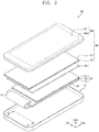
- FIG. 2 is an exploded perspective view showing the display device DD shown in FIG. 1
- FIG. 3 is a cross-sectional view showing the display device DD shown in FIG. 1 .
- the display device DD includes a display panel DP, a cover unit WU, and a cover member CP.
- the display panel DP includes a display area overlapped with the display area DR shown in FIG. 1 of the display device DD and a non-display area overlapped with the non-display area NDR shown in FIG. 1 of the display device DD.
- the display panel DP provides an image corresponding to image data input through the display area.
- the display panel DP may be, but not limited to, an organic light emitting display panel, a liquid crystal display panel, a plasma display panel, an electrophoretic display panel, or an electrowetting display panel. In the present exemplary embodiment, the organic light emitting display panel will be described as an example of the display panel DP without deviating from the scope of the present disclosure.
- the display panel DP includes a base substrate BS, a circuit layer ML, an organic light emitting element layer EL, an encapsulation layer ECL, a pad part PAD, and a touch sensing unit TS.
- the base substrate BS includes at least one of a glass substrate, a sapphire substrate, and a plastic substrate.
- the circuit layer ML, the organic light emitting element layer EL, the encapsulation layer ECL, the pad part PAD, and the touch sensing unit TS are sequentially stacked on the base substrate BS.
- the circuit layer ML includes a plurality of signal lines and a plurality of electronic devices that are arranged on the display panel DP.
- the circuit layer ML includes thin film transistors corresponding to gate lines, data lines, and pixels, respectively.
- the organic light emitting element layer EL generates a light having a color corresponding to a light emitting material included in the organic light emitting element layer EL.
- the color emitted by the organic light emitting element layer EL may include red, green, blue, and white colors, but it should not be limited thereto or thereby.
- the encapsulation layer ECL includes a thin film encapsulation layer (TFE) configured to include a plurality of inorganic thin film layers and a plurality of organic thin film layers.
- TFE thin film encapsulation layer
- the encapsulation layer ECL covers the organic light emitting element layer EL and blocks air and moisture to protect the organic light emitting element layer EL.
- the encapsulation layer ECL may be replaced with an encapsulation substrate.
- the encapsulation layer ECL is disposed spaced apart from the base substrate BS such that the organic light emitting element layer EL is disposed between the encapsulation layer ECL and the base substrate BS.
- the encapsulation layer ECL and the base substrate BS are coupled to each other by a sealant arranged along an edge of the base substrate BS.
- the touch sensing unit TS is disposed on the encapsulation layer ECL.
- the position of the touch sensing unit TS should not be limited thereto or thereby.
- the touch sensing unit TS may be disposed between the organic light emitting element layer EL and the encapsulation layer ECL or between the base substrate BS and the circuit layer ML.
- the touch sensing unit TS may be included in the cover unit WU other than the display panel DP.
- the touch sensing unit TS obtains coordinate information of a touch input position.
- the touch sensing unit TS may be any of a resistive film type, an electrostatic capacitive type, and an electromagnetic induction type depending on the touch sensing mechanism.
- the touch sensing unit TS may obtain the coordinate information of the touch input position using two kinds of sensor crossing each other in a self-capacitance manner or a mutual capacitance manner.
- the electrostatic capacitive type touch sensing unit will be described as an example of the touch sensing unit IT without deviating from the scope of the present disclosure.
- the display panel DP may include an optical member (not shown).
- the optical member may be disposed above the touch sensing unit TS, but it should not be limited thereto or thereby.
- the optical member may include at least one of a retardation plate and a polarizing plate.
- the polarizing plate is disposed on the retardation plate.
- An external light incident to the cover unit WU can be linearly polarized while passing through the polarizing plate.
- the linearly-polarized incident light can be reflected after passing through the retardation plate and incident to the polarizing plate after passing through the retardation plate again.
- the linearly-polarized incident light can be circularly polarized to have a phase difference of about 45 degrees while passing through the retardation plate to change the phase of the linearly-polarized incident light.
- the external light may not pass through the polarizing plate after passing again through the retardation plate, and the external light becomes extinct.
- a light that is right circularly polarized while passing through the retardation plate can be reflected and changed to a left circularly polarized light, and the right circularly polarized light can destructively interfere with the left circularly polarized light. Accordingly, a reflectance of the display device DD with respect to the external light may be reduced.
- the pad part PAD includes pads corresponding to and electrically connected to a plurality of signal lines that are electrically connected to the pixels in a one-to-one correspondence.
- the pad part PAD is electrically connected to a flexible printed circuit board FC.
- the flexible printed circuit board FC is attached to one end of the display panel DP and bent to a rear surface of the display panel DP.
- the flexible printed circuit board FC is electrically connected to the pad part PAD to receive signals from a driving printed circuit board PCB to drive the display panel DP.
- the flexible circuit board FC may apply the signals to the display panel DP.
- a data driving chip (not shown) may be mounted on one surface of the flexible printed circuit board FC. The data driving chip may generate data signals applied to the data lines of the display panel DP in response to an external signal.
- the driving printed circuit board PCB is disposed on the rear surface of the display panel DP.
- the driving printed circuit board PCB is electrically connected to the display panel DP through the flexible printed circuit board FC.
- the driving printed circuit board PCB may apply an image signal to display an image on the display panel DP and a control signal to control a drive of the display panel DP.
- the driving printed circuit board PCB includes a base substrate, and the base substrate may be a flexible printed circuit board.
- the base substrate may be, but not limited to, a flexible plastic substrate formed of polyimide or polyester.
- a protective member PP is disposed between the display panel DP and the driving printed circuit board PCB.
- the protective member PP may include at least one of a buffer member and a heat discharge member.
- the buffer member includes a material having high impact absorption.
- the buffer member includes a polymer resin such as polyurethane, polycarbonate, polypropylene, and polyethylene, or a sponge formed by foam molding, a rubber solution, an urethane-based material, or an acrylic-based material.
- the heat discharge member includes at least one of graphite, copper (Cu), and aluminum (Al) that exhibit superior heat discharge characteristics, but it should not be limited thereto or thereby.
- the heat discharge member may improve the heat discharge characteristics and may also have electromagnetic shielding characteristics and/or electromagnetic absorbing characteristics.
- the cover unit WU is disposed above the display panel DP.
- the cover unit WU and the display panel DP are attached to each other by an adhesive layer AL2.
- the adhesive layer AL2 may be, but is not limited to, an optically clear adhesive film or a layer made of an optical clear resin.
- the adhesive layer AL2 may be omitted according to some embodiments of the present disclosure. In this case, the cover unit WU and the display panel DP may make contact with each other without the adhesive layer AL2 and are disposed spaced apart from each other.
- the cover unit WU includes a first base member WD, an adhesive layer AL1, and a second base member BF.
- the first base member WD has a display area DA overlapped with the display area DR of the display device DD and a non-display area NDA overlapped with the non-display area NDR of the display device DD shown in FIG. 1 .
- the first base member WD may include at least one of a silicon substrate, a glass substrate, a sapphire substrate, and a plastic film, but it should not be limited thereto or thereby.
- the second base member BF may be a transparent film through which light transmits.
- the second base member BF may not completely transmit light.
- the light transmittance of the second base member BF may be lower than about 100%.
- the second base member BF may include one or more of synthetic resins such as PET, PVC, PP, PE, PC, and PMMA, but it should not be limited thereto or thereby.
- the adhesive layer AL1 is disposed between the first base member WD and the second base member BF. and the first base member WD and the second base member BF are attached to each other by the adhesive layer AL1.
- the adhesive layer AL1 may include an optically clear adhesive film or a layer made of an optical clear resin.
- the adhesive layer AL1 may include a hard coating layer (not shown).
- the cover member CP accommodates the display panel DP and is coupled to the cover unit WU.
- the cover member CP is formed by assembling plural parts or is integrally formed in a single unitary and individual unit, for example, by an injection molding method.
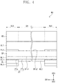
- FIG. 4 is a cross-sectional view taken along a line I-I' of FIG. 1 , according to one embodiment.
- FIG. 4 shows only the cover unit WU, and the display panel DP and the cover member CP are omitted.
- the cover unit WU includes the first base member WD, the adhesive layer AL1, the second base member BF, a reflective layer PL1, a color layer PL2, a pattern layer ML1, a cover layer ML2, and a shielding layer BL.
- the first base member WD includes a first area NDA and a second area DA defined on a plane.
- the first area NDA is overlapped with the non-display area NDR of FIG. 1 when viewed in a plan view
- the second area DA is overlapped with the display area DR of FIG. 1 when viewed in a plan view.
- the second base member BF is disposed under the first base member WD. That is, the second base member BF is disposed between the first base member WD and the display panel DP shown in FIG. 2 .
- the second base member BF includes a first surface BFs1 and a second surface BFs2 facing each other.
- the second surface BFs2 is disposed between the first base member WD and the first surface BFs1.
- the pattern layer ML1 is disposed under the first surface BFs1 of the second base member BF.
- the pattern layer ML1 may be directly disposed on the first surface BFs1 of the second base member BF, or an intermediate layer may exist between the pattern layer ML1 and the first surface BFs1 of the second base member BF.
- the pattern layer ML1 may include a light-curable material or a heat-curable material.
- the pattern layer ML1 includes an ultraviolet ray-curable resin.
- the pattern PT includes a first pattern PTa overlapped with the first area NDA and a second pattern PTb overlapped with the second area DA when viewed in the third direction DR3.
- the first pattern PTa diffusively reflects the light incident from the outside.
- FIG. 4 shows the first pattern PTa having a prism shape.
- the first pattern PTa may have various patterns, and the shape of the first pattern PTa should not be limited to the prism shape.
- the first pattern PTa is a three-dimensional pattern such as a fine hair line pattern, a wave pattern.
- the reflective layer PL1 is disposed under the first pattern PTa.
- the reflective layer PL1 is disposed to overlap with the first area NDA when viewed in a plan view.
- the reflective layer PL1 may include a reflective material.
- the reflective layer PL1 can reflect or absorb the light incident from the outside.
- the reflective layer PL1 may have a layer structure in which one or more layers are stacked.
- the reflective layer PL1 includes a first layer including indium and a second layer including titanium dioxide, but it should not be limited thereto or thereby.
- the shielding layer BL is disposed under the reflective layer PL1.
- the shielding layer BL may have a black color, but it should not be limited thereto or thereby.
- the shielding layer BL is disposed under the reflective layer PL1 to exhibit a color of a portion of the cover unit WU more clearly.
- the shielding layer BL may be formed on a lower surface of the reflective layer PL1 through a printing process, but it should not be limited thereto or thereby.
- the shielding layer BL may be implemented by a predetermined auxiliary member. In this case, the shielding layer BL may be attached to a lower portion of the reflective layer PL1.
- the cover unit WU is shown to include the shielding layer BL, but the shielding layer BL may be omitted according to other embodiments.
- the cover layer ML2 is disposed under the pattern layer ML1.
- the cover layer ML2 may include substantially the same material as the pattern layer ML1.
- the cover layer ML2 includes an ultraviolet ray-curable resin.
- the cover layer ML2 may also be attached to the second pattern PTb of the pattern layer ML1. Accordingly, the light is not diffusively reflected by the second pattern PTb overlapped with the second area DA when viewed in a plan view.
- a portion of the cover layer ML2 is disposed under the shielding layer BL, and the other portion of the cover layer ML2 is disposed under the pattern layer ML1.
- the cover layer ML2 may be disposed only under the second pattern PTb of the pattern layer ML1.
- the cover layer ML2 may be disposed to cover the reflective layer PL1 and the second pattern PTb, and the shielding layer BL may be disposed under the cover layer ML2 overlapping only the portion of the cover layer ML2 in the first area NDA when viewed in a plan view.
- the color layer PL2 is disposed above the second surface BFs2 of the second base member BF.
- the color layer PL2 is disposed between the first base member WD and the second base member BF. Accordingly, the reflective layer PL1 and the color layer PL2 face each other such that the second base member BF is disposed between the reflective layer PL1 and the color layer PL2.
- the color layer PL2 may be directly disposed on the second base member BF.
- the color layer PL2 may be overlapped with the first area NDA and the reflective layer PL1 when viewed in a plan view.
- the color layer PL2 has a light transmittance. Thus, the light incident from the outside passes through the color layer PL2 and is reflected by the reflective layer PL1. Accordingly, a user may recognize a color that optically combines a color of the reflective layer PL1 and a color of the color layer PL2.
- the color layer PL2 may include a dye having a predetermined color and a permeable material.
- the light transmittance of the color layer PL2 may be controlled by adjusting a concentration of the dye and the permeable material.
- the cover unit WU may have various colors by changing the color of the color layer PL2.
- compositions included in the reflective layer PL1 and/or the color layer PL2 may be changed.
- the various colors can be implemented by changing the color layer PL2 to include different materials in accordance with the color implemented by the cover unit WU.
- the reflective layer PL1 may serve as a common layer, and the color and/or composition of the reflective layer PL1 may not change.
- the reflective layer PL1 may be used to impart a special visual effect, for example, a metallic effect in the portion of the cover unit WU corresponding to the first area NDA.
- the color of the cover unit WU may be changed in the portion of the cover unit WU corresponding to the first area NDA by changing the color of the color layer PL2.
- the color of the cover unit WU may be determined by optical combination of the variable color of the color layer PL2 and the intrinsic color of the reflective layer PL1 that is determined by the optical characteristic of the material(s) forming the reflective layer PL1.
- the material of the reflective layer PL1 is not related to the color of the portion of the cover unit WU. Accordingly, various colors of the cover unit WU may be implemented only by changing the color of the color layer PL2. That is, processes to impart a special visual effect and implement a specific color of the cover unit WU are simplified and separated, and thus a variation in color between cover units representing the same color can be reduced. Thus, the product manufacturing yield may be improved.
- FIG. 5 is a cross-sectional view taken along a line I-I' of FIG. 1 , according to one embodiment.
- a cover unit WUa shown in FIG. 5 may have the same structure and function as those of the cover unit WU shown in FIG. 4 except for a shape of a pattern layer ML1a.
- the reflective layer PL1 having a pattern PTa is disposed on one surface of the pattern layer ML1a.
- the pattern PTa is overlapped only with the first area NDA when viewed in a plan view.
- the surface fp of the pattern layer ML1a that is overlapped with the second area DA may be flat. Accordingly, the cover layer ML2 shown in FIG. 4 that flattens the pattern PTb of the pattern layer ML1a in an area overlapped with the second area DA may be omitted.
- FIG. 6 is a cross-sectional view taken along a line I-I' of FIG. 1 , according to one embodiment.
- a cover unit WUb shown in FIG. 6 may have the same structure and function as those of the cover unit WU shown in FIG. 4 except for a shape of a pattern layer ML1b.
- the pattern layer ML1 shown in FIG. 4 is overlapped with the first and second areas NDA and DA when viewed in a plan view, but the pattern layer ML1b shown in FIG. 6 is overlapped with the first area NDA and not overlapped with the second area DA when viewed in a plan view. Accordingly, the transmittance of the light provided from the display panel DP shown in FIG. 2 may be further improved.
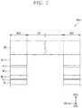
- FIG. 7 is a cross-sectional view taken along a line I-I' of FIG. 1 , according to one embodiment.
- a cover unit WUc shown in FIG. 7 may have the same structure and function as those of the cover unit WU shown in FIG. 4 except for shapes of a pattern layer ML1c, a second base member BFc, and an adhesive layer AL1c
- Each of the pattern layer ML1c, the second base member BFc, and the adhesive layer AL1c shown in FIG. 7 is overlapped with the first area NDA and not overlapped with the second area DA when viewed in a plan view. Accordingly, the transmittance of the light provided from the display panel DP shown in FIG. 2 may be further improved.
- FIG. 8 is a cross-sectional view taken along a line I-I' of FIG. 1 , according to one embodiment.
- a cover unit WUd shown in FIG. 8 may not include the pattern layer ML1 and the cover layer ML2 shown in FIG. 4 when compared with the cover unit WU shown in FIG. 4 .
- a thickness of the cover unit WUd may be reduced compared with the cover unit WU described with reference to FIG. 4 , and the transmittance of the light provided from the display panel DP shown in FIG. 2 may be further improved.
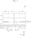
- FIG. 9 is a cross-sectional view taken along a line I-I' of FIG. 1 , according to one embodiment.
- a cover unit WUe shown in FIG. 9 may have the same structure and function as those of the cover unit WU shown in FIG. 4 except for a color layer PL2a.
- the color layer PL2a may include a primer layer PL and a color implementing layer CCa.
- the primer layer PL is disposed on the second base member BF, and the color implementing layer CCa is disposed on the primer layer PL.
- An adhesive force between the color implementing layer CCa and the second base member BF may be further improved by the primer layer PL.
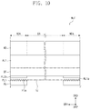
- FIG. 10 is a cross-sectional view taken along a line I-I' of FIG. 1 , according to one embodiment.
- a cover unit WUf shown in FIG. 10 may have the same structure and function as those of the cover unit WUa shown in FIG. 5 except for a position of a color layer PL2b.
- the color layer PL2b is disposed between the pattern layer ML1a and the second base member BF. That is, the color layer PL2b and the reflective layer PL1 may be disposed on the same surface of the second base member BF.
- the 10 may have structures in which the positions of the second base member BF and the color layer PL2 (or PL2a) are changed with respect to each other in the cover units WU, WUa, WUb, WUc, WUd, and WUe described with reference to FIGS. 4 to 9 .
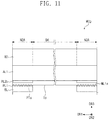
- FIG. 11 is a cross-sectional view taken along a line I-I' of FIG. 1 , according to one embodiment.
- a cover unit WUg shown in FIG. 11 does not include the second base member BF when compared with the cover unit WUf shown in FIG. 10 .
- the cover unit WUg may be thinner, and the flexibility of the cover unit WUg may be improved.
- the cover unit WUg shown in FIG. 11 may have structures in which the positions of the second base member BF and the color layer PL2 (or PL2a) are changed with respect to each other, or the second base member BF is omitted in the cover units WU, WUa, WUb, WUc, WUd, and WUe described with reference to FIGS. 4 to 9 .
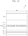
- FIG. 12 is a cross-sectional view taken along a line II-II' of FIG. 1 , according to one embodiment.
- the cross-sectional view shown in FIG. 12 is taken along an area in which a logo LL is formed.
- FIG. 12 shows only the cover unit WU, and the display panel DP and the cover member CP are omitted.
- a color layer PL2b includes a logo layer LP and a color implementation layer CC.
- the logo layer LP is disposed on the second base member BF, and the color implementation layer CC covers the logo layer LP and implements the color of the cover unit WU in the first area NDA.
- the logo layer LP may be disposed on the second base member BF using a printing method, but it should not be limited thereto or thereby.
- the logo layer LP may be disposed at various layer and/or positions in the first area NDA of the cover unit WU.
- the logo layer LP may be disposed between the first base member WD and the adhesive layer AL1.
- the cover units WU and WUa to WUg shown in FIGS. 4 to 12 are disposed in the third direction DR3 in which the display panel DP provides an image. Accordingly, the image is displayed by the display panel DP to the user after passing through the cover units WU and WUa to WUg, respectively.
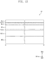
- FIG. 13 is a cross-sectional view taken along a line II-II' of FIG. 1 , according to one embodiment.
- FIG. 13 shows only the cover member CP and the display panel DP and the cover unit WU are omitted.
- the cover member CP may also be referred to as a cover unit.
- the cover member CP includes a first base member WDx, an adhesive layer AL1x, a second base member BFx, a reflective layer PL1x, a color layer PL2x, a base layer MLx, and a shielding layer BLx.
- the cover member CP may not include an area through which the image transmits. Accordingly, each of the reflective layer PL1x and the color layer PL2x of the cover member CP may be overlapped with an entire surface of the first base member WDx. Similar to the color layer PL2, PL2a, and PL2b of the cover unit WU and WU1 to WUg shown in FIGS.
- the color layer PL2x of the cover member CP may be used to implement a color of the cover member CP, and the reflective layer PL1x may be used to impart a visual special effect (e.g ., a metallic effect) of the cover member CP.
- a visual special effect e.g ., a metallic effect
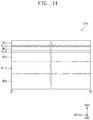
- FIG. 14 is a cross-sectional view taken along a line III-III' of FIG. 2 , according to another embodiment.
- a cover member CPa shown in FIG. 14 may have the same structure and function as those of the cover member CP shown in FIG. 13 except for a position of a color layer PL2y.
- the color layer PL2y is disposed between the second base member BFx and the base layer MLx. That is, the color layer PL2y and the reflective layer PL1x may be disposed on the same surface of the second base member BFx.
- the second base member BFx may be omitted according to another embodiment.
- the color layer PL2y may be directly disposed on the adhesive layer AL1x.
- the adhesive layer AL1x may further include a hard coating layer, according to one embodiment.
- FIG. 15 is a flowchart showing a method of forming a cover unit, according to one exemplary embodiment of the present disclosure
- FIG. 16 is a view showing a method of forming a cover unit, according to one exemplary embodiment of the present disclosure
- FIG. 17 is a view showing a method of forming a cover unit, according to another exemplary embodiment of the present disclosure.
- a second base member MBF is prepared (S100).
- the second base member MBF may be provided while being rolled on a roller.
- the second base member MBF may be cut later to have substantially the same shape as that of the second base member BF shown in FIG. 4 .
- the pattern layer ML1 is formed on the first surface BFs1 of the second base member MBF (S200).
- the pattern layer ML1 is formed by a roll-to-roll imprint process.
- a light-curable resin is provided onto the first surface BFs1 of the second base member MBF, and the surface provided with the light-curable resin is pressed by a pattern roll RL1.
- the ultraviolet ray is irradiated onto the light-curable resin to cure the light-curable resin, and thus the pattern PT is formed on the pattern layer ML1.
- a pattern corresponding to the pattern PT is formed on the pattern roll RL1.
- a film provided with a pattern corresponding to the pattern PT is provided on the pattern roll RL1.
- various manufacturing processes and methods can be used to form the pattern layer ML1, and the manufacturing process and method of forming the pattern layer ML1 should not be limited to or by these examples.
- the reflective layer PL1 is formed on the pattern layer ML1 (S300).
- the reflective layer PL1 is formed through a depositing process.
- FIG. 16 shows only one deposition source, but the number of the depositing sources should not be limited to one.
- the reflective layer PL1 may include a plurality of layers, and thus the number of the depositing sources may increase.
- the reflective layer PL1 may serve as a common layer, and the color and/or composition of the reflective layer PL1 may not be changed to implement a different color of the cover unit WU and/or the cover member CP.
- the pattern layer ML1 and the reflective layer PL1 may be formed through a common process regardless of a color implemented by the cover unit WU and/or the cover member CP. As a result, processes shown in FIG. 16 may be common regardless of the color of the cover unit WU.
- the color layer PL2 is formed on the second surface BFs2 of the second base member MBF, on which the pattern layer ML1 and the reflective layer PL1 are formed (S400).
- the color layer PL2 is used to implement the color of the cover unit WU.
- the color layer PL2 is formed by a transfer method.
- the color layer PL2 may be formed by various methods including, but not limited to, a silk screen printing method, and a digital printing method.
- the formation of the color layer PL2 by the transfer method may reduce process and/or color variations to implement the color of the cover unit WU.
- process variations may occur depending on the position of the second base member in the deposition chamber because a physical condition may vary within a single deposition chamber and/or in different deposition chambers.
- the color layer PL2 is formed by a roll-to-roll process, and thus the process variations that may be caused by the varying conditions of the deposition chamber and the position of the second base member in the deposition chamber may be reduced. Accordingly, the color difference of the cover unit WU is reduced, and the product manufacturing yield may be improved.
- the adhesive layer AL1 is formed to cover the color layer PL2 (S500).
- the adhesive layer AL1 may be an optically clear adhesive film.
- the optically clear adhesive film may be provided while the second base member MBF is rolled on a roller RL2. When the second base member MBF moves, the optically clear adhesive film rolled on the roller RL2 is attached to the second base member MBF.
- FIGS. 16 and 17 show the cover unit continuously formed through a roll-to-roll process as a representative example.
- various other processes may be applied to manufacture a cover unit, and the method of forming the cover unit should not be limited to or by the exemplary embodiments described herein.
- the cover unit may be formed by a batch process in a predetermined unit of sheets.
Landscapes
- Physics & Mathematics (AREA)
- Engineering & Computer Science (AREA)
- Optics & Photonics (AREA)
- General Physics & Mathematics (AREA)
- Nonlinear Science (AREA)
- General Engineering & Computer Science (AREA)
- Theoretical Computer Science (AREA)
- Signal Processing (AREA)
- Microelectronics & Electronic Packaging (AREA)
- Mathematical Physics (AREA)
- Chemical & Material Sciences (AREA)
- Crystallography & Structural Chemistry (AREA)
- Ceramic Engineering (AREA)
- Computer Hardware Design (AREA)
- Human Computer Interaction (AREA)
- Manufacturing & Machinery (AREA)
- Devices For Indicating Variable Information By Combining Individual Elements (AREA)
Abstract
Description
- The present disclosure relates to a cover unit and a display device having the same. More particularly, the present disclosure relates to a cover unit having improved manufacturing yield and a display device having the cover unit.
- A cover unit of a display device, such as a television, a laptop computer, a tablet personal computer (PC), and a smartphone, is placed on the outside of the display device. The cover unit can provide a color to an area corresponding to a non-display area surrounding a display area. As the design of a display device becomes as important as the performance, various structures of a cover unit and processes to manufacture the cover unit to implement various colors and visual effects have been developed.
- The present disclosure provides a cover unit having improved manufacturing yield and a display device having the cover unit.
- According to one embodiment, a display device includes a cover unit and a display panel disposed on the cover unit. The cover unit includes a first base member disposed on the display panel and including a first area and a second area when viewed in a plan view, a pattern layer disposed between the first base member and the display panel, a color layer disposed between the first base member and the pattern layer, and a reflective layer disposed between the display panel and the pattern layer.
- The reflective layer may be overlapped with the color layer when viewed in a plan view.
- The cover unit may further include a second base member disposed between the color layer and the pattern layer.
- The second base member may not be overlapped with the second area when viewed in a plan view.
- The color layer may include a primer layer disposed on the second base member and a color implementing layer disposed on the primer layer.
- The cover unit may further include a second base member disposed between the color layer and the first base member.
- The display panel may include a display area overlapped with the second area and displaying an image and a non-display area overlapped with the first area and not displaying the image. The reflective layer and the color layer may be overlapped with the first area when viewed in a plan view and may not be overlapped with the second area.
- The pattern layer may further include a pattern disposed on one surface of the pattern layer that makes contact with the reflective layer.
- The cover unit may further include a cover layer covering the pattern layer, and the pattern may be overlapped with the first area and the second area when viewed in a plan view.
- A portion of the pattern overlapped with the second area may be flat.
- The pattern maybe disposed only on a portion of the pattern layer that is overlapped with the first area when viewed in a plan view.
- The pattern layer may not be overlapped with the second area when viewed in a plan view.
- When the first area has a first color when viewed in a plan view, the reflective layer may have a second color, and the color layer may have a third color. When the first area has a fourth color that is different from the first color when viewed in a plan view, the reflective layer may have the second color, and the color layer may have a fifth color that is different from the third color.
- The cover unit may further include a shielding layer disposed between the reflective layer and the display panel, and the shielding layer may cover the reflective layer.
- The cover unit may further include an adhesive layer disposed between the color layer and the first base member.
- The adhesive layer may be overlapped with the first area and may not be overlapped with the second area when viewed in a plan view.
- The reflective layer may impart a metallic effect.
- The display device may further include a cover member disposed on a rear side of the display panel. The cover member may include a third base member, a second reflective layer, and a second color layer.
- According to one embodiment, a cover unit includes a first base member, a pattern layer disposed on the first base member, a reflective layer disposed on the pattern layer, and a color layer disposed between the first base member and the pattern layer.
- The cover unit may further include: an adhesive layer disposed between the color layer and the first base member; a second base member disposed between the color layer and the pattern layer or disposed between the color layer and the first base member; and a shielding layer covering the reflective layer.
- The cover unit may further include a cover layer covering the pattern layer.
- The first base member may include a first area and a second area when viewed in a plan view, and each of the reflective layer and the color layer may be overlapped with the first area and may not be overlapped with the second area when viewed in a plan view.
- The reflective layer may impart a metallic effect.
- The reflective layer may have a second color, and the color layer has a third color. The first area may implement a first color when viewed in a plan view by optically combining the second color of the reflective layer and the third color of the color layer.
- The reflective layer, the color layer, and the first base member may be overlapped with each other when viewed in a plan view.
- The cover unit may further include a second base member disposed between the color layer and the reflective layer, and the color layer may directly make contact with one surface of the second base member.
- A method for forming a cover unit include: forming a pattern layer including a pattern on a first surface of a base member by a roll-to-roll imprint process; forming a reflective layer on the pattern layer by a depositing process; forming a color layer on a second surface of the base member by a roll-to-roll process; and forming an adhesive layer to cover the color layer.
- The above and advantages of the present disclosure will become readily apparent by reference to the following detailed description in conjunction with the accompanying drawings wherein:
-
FIG. 1 is a perspective view showing a display device, according to one exemplary embodiment of the present disclosure; -
FIG. 2 is an exploded perspective view showing the display device shown inFIG. 1 ; -
FIG. 3 is a cross-sectional view showing the display device shown inFIG. 1 ; -
FIG. 4 is a cross-sectional view taken along a line I-I' ofFIG. 1 , according to one embodiment; -
FIG. 5 is a cross-sectional view taken along a line I-I' ofFIG. 1 , according to one embodiment; -
FIG. 6 is a cross-sectional view taken along a line I-I' ofFIG. 1 , according to one embodiment; -
FIG. 7 is a cross-sectional view taken along a line I-I' ofFIG. 1 , according to one embodiment; -
FIG. 8 is a cross-sectional view taken along a line I-I' ofFIG. 1 , according to one embodiment; -
FIG. 9 is a cross-sectional view taken along a line I-I' ofFIG. 1 , according to one embodiment; -
FIG. 10 is a cross-sectional view taken along a line I-I' ofFIG. 1 , according to one embodiment; -
FIG. 11 is a cross-sectional view taken along a line I-I' ofFIG. 1 , according to one embodiment; -
FIG. 12 is a cross-sectional view taken along a line II-II' ofFIG. 1 , according to one embodiment; -
FIG. 13 is a cross-sectional view taken along a line II-II' ofFIG. 1 , according to one embodiment; -
FIG. 14 is a cross-sectional view taken along a line III-III' ofFIG. 2 , according to another embodiment; -
FIG. 15 is a flowchart showing a method of forming a cover unit, according to one exemplary embodiment of the present disclosure; -
FIG. 16 is a view showing a method of forming a cover unit, according to one exemplary embodiment of the present disclosure; and -
FIG. 17 is a view showing a method of forming a cover unit, according to another exemplary embodiment of the present disclosure. - The following description with reference to the accompanying drawings is provided to assist in a comprehensive understanding of various embodiments of the present disclosure as defined by the claims and their equivalents. It includes various specific details to assist in that understanding but these are to be regarded as merely exemplary. In addition, descriptions of well-known functions and constructions may be omitted for clarity and conciseness. Like numerals refer to like elements throughout.
- Hereinafter, the present disclosure will be explained in detail with reference to the accompanying drawings.
-
FIG. 1 is a perspective view showing a display device DD, according to one exemplary embodiment of the present disclosure. For example, the display device DD is a flat mobile terminal. However, the display device DD may be applied to various display devices, such as a curved display device, a bendable display device, a reliable display device, a foldable display device, a stretchable display device, etc., according to some embodiment. The display device DD according to other exemplary embodiments may be applied to a large-sized electronic item such as a television set and an outdoor billboard and a small and medium-sized electronic item such as a personal computer, a notebook computer, a personal digital assistant, a car navigation unit, a game unit, a mobile electronic device, a wrist-type electronic device, and a camera. However, it is understood that the display DD can be applied to various other electronic items and applications and should not be limited to or by the examples listed herein. - The display device DD includes a plurality of areas distinct from each other on a display surface. For example, the display device DD includes a display area DR displaying an image IM and a non-display area NDR disposed adjacent to the display area DR. The display surface on which the image IM is displayed is substantially parallel to a surface defined by a first direction DR1 and a second direction DR2. A third direction DR3 indicates a normal direction of the display surface. The third direction DR3 may serve as a reference axis to distinct front and rear surfaces of each member of the display device DA. In the following descriptions, the surface defined by the first and second directions DR1 and DR2 may be referred to as a flat surface, and an expression of "when viewed in a plan view" may mean "when viewed in the third direction DR3".
-
FIG. 2 is an exploded perspective view showing the display device DD shown inFIG. 1 , andFIG. 3 is a cross-sectional view showing the display device DD shown inFIG. 1 . - Referring to
FIGS. 2 and3 , the display device DD includes a display panel DP, a cover unit WU, and a cover member CP. The display panel DP includes a display area overlapped with the display area DR shown inFIG. 1 of the display device DD and a non-display area overlapped with the non-display area NDR shown inFIG. 1 of the display device DD. The display panel DP provides an image corresponding to image data input through the display area. The display panel DP may be, but not limited to, an organic light emitting display panel, a liquid crystal display panel, a plasma display panel, an electrophoretic display panel, or an electrowetting display panel. In the present exemplary embodiment, the organic light emitting display panel will be described as an example of the display panel DP without deviating from the scope of the present disclosure. - The display panel DP includes a base substrate BS, a circuit layer ML, an organic light emitting element layer EL, an encapsulation layer ECL, a pad part PAD, and a touch sensing unit TS. The base substrate BS includes at least one of a glass substrate, a sapphire substrate, and a plastic substrate. The circuit layer ML, the organic light emitting element layer EL, the encapsulation layer ECL, the pad part PAD, and the touch sensing unit TS are sequentially stacked on the base substrate BS. The circuit layer ML includes a plurality of signal lines and a plurality of electronic devices that are arranged on the display panel DP. For example, the circuit layer ML includes thin film transistors corresponding to gate lines, data lines, and pixels, respectively.
- The organic light emitting element layer EL generates a light having a color corresponding to a light emitting material included in the organic light emitting element layer EL. The color emitted by the organic light emitting element layer EL may include red, green, blue, and white colors, but it should not be limited thereto or thereby.
- The encapsulation layer ECL includes a thin film encapsulation layer (TFE) configured to include a plurality of inorganic thin film layers and a plurality of organic thin film layers. The encapsulation layer ECL covers the organic light emitting element layer EL and blocks air and moisture to protect the organic light emitting element layer EL. In another embodiment, the encapsulation layer ECL may be replaced with an encapsulation substrate. The encapsulation layer ECL is disposed spaced apart from the base substrate BS such that the organic light emitting element layer EL is disposed between the encapsulation layer ECL and the base substrate BS. The encapsulation layer ECL and the base substrate BS are coupled to each other by a sealant arranged along an edge of the base substrate BS.
- The touch sensing unit TS is disposed on the encapsulation layer ECL. The position of the touch sensing unit TS should not be limited thereto or thereby. For example, the touch sensing unit TS may be disposed between the organic light emitting element layer EL and the encapsulation layer ECL or between the base substrate BS and the circuit layer ML. In another example, the touch sensing unit TS may be included in the cover unit WU other than the display panel DP.
- The touch sensing unit TS obtains coordinate information of a touch input position. The touch sensing unit TS may be any of a resistive film type, an electrostatic capacitive type, and an electromagnetic induction type depending on the touch sensing mechanism. In the electrostatic capacitive type touch sensing unit, the touch sensing unit TS may obtain the coordinate information of the touch input position using two kinds of sensor crossing each other in a self-capacitance manner or a mutual capacitance manner. In the present exemplary embodiment, the electrostatic capacitive type touch sensing unit will be described as an example of the touch sensing unit IT without deviating from the scope of the present disclosure.
- According to one embodiment, the display panel DP may include an optical member (not shown). The optical member may be disposed above the touch sensing unit TS, but it should not be limited thereto or thereby. The optical member may include at least one of a retardation plate and a polarizing plate. In the case that the optical member includes both the retardation plate and the polarizing plate, the polarizing plate is disposed on the retardation plate. An external light incident to the cover unit WU can be linearly polarized while passing through the polarizing plate. The linearly-polarized incident light can be reflected after passing through the retardation plate and incident to the polarizing plate after passing through the retardation plate again. The linearly-polarized incident light can be circularly polarized to have a phase difference of about 45 degrees while passing through the retardation plate to change the phase of the linearly-polarized incident light. As a result, the external light may not pass through the polarizing plate after passing again through the retardation plate, and the external light becomes extinct. For example, a light that is right circularly polarized while passing through the retardation plate can be reflected and changed to a left circularly polarized light, and the right circularly polarized light can destructively interfere with the left circularly polarized light. Accordingly, a reflectance of the display device DD with respect to the external light may be reduced.
- The pad part PAD includes pads corresponding to and electrically connected to a plurality of signal lines that are electrically connected to the pixels in a one-to-one correspondence. The pad part PAD is electrically connected to a flexible printed circuit board FC.
- The flexible printed circuit board FC is attached to one end of the display panel DP and bent to a rear surface of the display panel DP. The flexible printed circuit board FC is electrically connected to the pad part PAD to receive signals from a driving printed circuit board PCB to drive the display panel DP. In addition, the flexible circuit board FC may apply the signals to the display panel DP. A data driving chip (not shown) may be mounted on one surface of the flexible printed circuit board FC. The data driving chip may generate data signals applied to the data lines of the display panel DP in response to an external signal.
- The driving printed circuit board PCB is disposed on the rear surface of the display panel DP. The driving printed circuit board PCB is electrically connected to the display panel DP through the flexible printed circuit board FC. The driving printed circuit board PCB may apply an image signal to display an image on the display panel DP and a control signal to control a drive of the display panel DP.
- The driving printed circuit board PCB includes a base substrate, and the base substrate may be a flexible printed circuit board. In this case, the base substrate may be, but not limited to, a flexible plastic substrate formed of polyimide or polyester.
- A protective member PP is disposed between the display panel DP and the driving printed circuit board PCB. The protective member PP may include at least one of a buffer member and a heat discharge member. The buffer member includes a material having high impact absorption. For example, the buffer member includes a polymer resin such as polyurethane, polycarbonate, polypropylene, and polyethylene, or a sponge formed by foam molding, a rubber solution, an urethane-based material, or an acrylic-based material. The heat discharge member includes at least one of graphite, copper (Cu), and aluminum (Al) that exhibit superior heat discharge characteristics, but it should not be limited thereto or thereby. The heat discharge member may improve the heat discharge characteristics and may also have electromagnetic shielding characteristics and/or electromagnetic absorbing characteristics.
- The cover unit WU is disposed above the display panel DP. The cover unit WU and the display panel DP are attached to each other by an adhesive layer AL2. The adhesive layer AL2 may be, but is not limited to, an optically clear adhesive film or a layer made of an optical clear resin. The adhesive layer AL2 may be omitted according to some embodiments of the present disclosure. In this case, the cover unit WU and the display panel DP may make contact with each other without the adhesive layer AL2 and are disposed spaced apart from each other.
- The cover unit WU includes a first base member WD, an adhesive layer AL1, and a second base member BF. Referring to
FIG. 2 , the first base member WD has a display area DA overlapped with the display area DR of the display device DD and a non-display area NDA overlapped with the non-display area NDR of the display device DD shown inFIG. 1 . - The first base member WD may include at least one of a silicon substrate, a glass substrate, a sapphire substrate, and a plastic film, but it should not be limited thereto or thereby. The second base member BF may be a transparent film through which light transmits. The second base member BF may not completely transmit light. For example, the light transmittance of the second base member BF may be lower than about 100%. The second base member BF may include one or more of synthetic resins such as PET, PVC, PP, PE, PC, and PMMA, but it should not be limited thereto or thereby.
- The adhesive layer AL1 is disposed between the first base member WD and the second base member BF. and the first base member WD and the second base member BF are attached to each other by the adhesive layer AL1. The adhesive layer AL1 may include an optically clear adhesive film or a layer made of an optical clear resin. In addition, the adhesive layer AL1 may include a hard coating layer (not shown).
- The cover member CP accommodates the display panel DP and is coupled to the cover unit WU. The cover member CP is formed by assembling plural parts or is integrally formed in a single unitary and individual unit, for example, by an injection molding method.
-
FIG. 4 is a cross-sectional view taken along a line I-I' ofFIG. 1 , according to one embodiment.FIG. 4 shows only the cover unit WU, and the display panel DP and the cover member CP are omitted. - Referring to
FIG. 4 , the cover unit WU includes the first base member WD, the adhesive layer AL1, the second base member BF, a reflective layer PL1, a color layer PL2, a pattern layer ML1, a cover layer ML2, and a shielding layer BL. The first base member WD includes a first area NDA and a second area DA defined on a plane. The first area NDA is overlapped with the non-display area NDR ofFIG. 1 when viewed in a plan view, and the second area DA is overlapped with the display area DR ofFIG. 1 when viewed in a plan view. - The second base member BF is disposed under the first base member WD. That is, the second base member BF is disposed between the first base member WD and the display panel DP shown in
FIG. 2 . The second base member BF includes a first surface BFs1 and a second surface BFs2 facing each other. The second surface BFs2 is disposed between the first base member WD and the first surface BFs1. - The pattern layer ML1 is disposed under the first surface BFs1 of the second base member BF. The pattern layer ML1 may be directly disposed on the first surface BFs1 of the second base member BF, or an intermediate layer may exist between the pattern layer ML1 and the first surface BFs1 of the second base member BF. The pattern layer ML1 may include a light-curable material or a heat-curable material. For example, the pattern layer ML1 includes an ultraviolet ray-curable resin.
- One surface of the pattern layer ML1 may contact with the second base member BF, and a pattern PT is formed on the other surface of the pattern layer ML1. The pattern PT includes a first pattern PTa overlapped with the first area NDA and a second pattern PTb overlapped with the second area DA when viewed in the third direction DR3.
- The first pattern PTa diffusively reflects the light incident from the outside.
FIG. 4 shows the first pattern PTa having a prism shape. However, it is understood that the first pattern PTa may have various patterns, and the shape of the first pattern PTa should not be limited to the prism shape. For example, the first pattern PTa is a three-dimensional pattern such as a fine hair line pattern, a wave pattern. - The reflective layer PL1 is disposed under the first pattern PTa. The reflective layer PL1 is disposed to overlap with the first area NDA when viewed in a plan view. The reflective layer PL1 may include a reflective material. The reflective layer PL1 can reflect or absorb the light incident from the outside. The reflective layer PL1 may have a layer structure in which one or more layers are stacked. For example, the reflective layer PL1 includes a first layer including indium and a second layer including titanium dioxide, but it should not be limited thereto or thereby.
- The shielding layer BL is disposed under the reflective layer PL1. The shielding layer BL may have a black color, but it should not be limited thereto or thereby. The shielding layer BL is disposed under the reflective layer PL1 to exhibit a color of a portion of the cover unit WU more clearly.
- The shielding layer BL may be formed on a lower surface of the reflective layer PL1 through a printing process, but it should not be limited thereto or thereby. The shielding layer BL may be implemented by a predetermined auxiliary member. In this case, the shielding layer BL may be attached to a lower portion of the reflective layer PL1. In
FIG. 4 , the cover unit WU is shown to include the shielding layer BL, but the shielding layer BL may be omitted according to other embodiments. - The cover layer ML2 is disposed under the pattern layer ML1. The cover layer ML2 may include substantially the same material as the pattern layer ML1. For example, the cover layer ML2 includes an ultraviolet ray-curable resin. The cover layer ML2 may also be attached to the second pattern PTb of the pattern layer ML1. Accordingly, the light is not diffusively reflected by the second pattern PTb overlapped with the second area DA when viewed in a plan view.
- In
FIG. 4 , a portion of the cover layer ML2 is disposed under the shielding layer BL, and the other portion of the cover layer ML2 is disposed under the pattern layer ML1. However, the cover layer ML2 may be disposed only under the second pattern PTb of the pattern layer ML1. According to another embodiment, the cover layer ML2 may be disposed to cover the reflective layer PL1 and the second pattern PTb, and the shielding layer BL may be disposed under the cover layer ML2 overlapping only the portion of the cover layer ML2 in the first area NDA when viewed in a plan view. - The color layer PL2 is disposed above the second surface BFs2 of the second base member BF. The color layer PL2 is disposed between the first base member WD and the second base member BF. Accordingly, the reflective layer PL1 and the color layer PL2 face each other such that the second base member BF is disposed between the reflective layer PL1 and the color layer PL2. The color layer PL2 may be directly disposed on the second base member BF. The color layer PL2 may be overlapped with the first area NDA and the reflective layer PL1 when viewed in a plan view.
- The color layer PL2 has a light transmittance. Thus, the light incident from the outside passes through the color layer PL2 and is reflected by the reflective layer PL1. Accordingly, a user may recognize a color that optically combines a color of the reflective layer PL1 and a color of the color layer PL2.
- The color layer PL2 may include a dye having a predetermined color and a permeable material. The light transmittance of the color layer PL2 may be controlled by adjusting a concentration of the dye and the permeable material.
- The cover unit WU may have various colors by changing the color of the color layer PL2. To implement various colors in the portion of the cover unit WU corresponding to the first area NDA, compositions included in the reflective layer PL1 and/or the color layer PL2 may be changed. According to the present exemplary embodiment, the various colors can be implemented by changing the color layer PL2 to include different materials in accordance with the color implemented by the cover unit WU. In this case, the reflective layer PL1 may serve as a common layer, and the color and/or composition of the reflective layer PL1 may not change. Instead, the reflective layer PL1 may be used to impart a special visual effect, for example, a metallic effect in the portion of the cover unit WU corresponding to the first area NDA. The color of the cover unit WU may be changed in the portion of the cover unit WU corresponding to the first area NDA by changing the color of the color layer PL2. The color of the cover unit WU may be determined by optical combination of the variable color of the color layer PL2 and the intrinsic color of the reflective layer PL1 that is determined by the optical characteristic of the material(s) forming the reflective layer PL1.
- According to the present exemplary embodiment, the material of the reflective layer PL1 is not related to the color of the portion of the cover unit WU. Accordingly, various colors of the cover unit WU may be implemented only by changing the color of the color layer PL2. That is, processes to impart a special visual effect and implement a specific color of the cover unit WU are simplified and separated, and thus a variation in color between cover units representing the same color can be reduced. Thus, the product manufacturing yield may be improved.
-
FIG. 5 is a cross-sectional view taken along a line I-I' ofFIG. 1 , according to one embodiment. A cover unit WUa shown inFIG. 5 may have the same structure and function as those of the cover unit WU shown inFIG. 4 except for a shape of a pattern layer ML1a. - Referring to
FIG. 5 , the reflective layer PL1 having a pattern PTa is disposed on one surface of the pattern layer ML1a. The pattern PTa is overlapped only with the first area NDA when viewed in a plan view. The surface fp of the pattern layer ML1a that is overlapped with the second area DA may be flat. Accordingly, the cover layer ML2 shown inFIG. 4 that flattens the pattern PTb of the pattern layer ML1a in an area overlapped with the second area DA may be omitted. -
FIG. 6 is a cross-sectional view taken along a line I-I' ofFIG. 1 , according to one embodiment. A cover unit WUb shown inFIG. 6 may have the same structure and function as those of the cover unit WU shown inFIG. 4 except for a shape of a pattern layer ML1b. The pattern layer ML1 shown inFIG. 4 is overlapped with the first and second areas NDA and DA when viewed in a plan view, but the pattern layer ML1b shown inFIG. 6 is overlapped with the first area NDA and not overlapped with the second area DA when viewed in a plan view. Accordingly, the transmittance of the light provided from the display panel DP shown inFIG. 2 may be further improved. -
FIG. 7 is a cross-sectional view taken along a line I-I' ofFIG. 1 , according to one embodiment. A cover unit WUc shown inFIG. 7 may have the same structure and function as those of the cover unit WU shown inFIG. 4 except for shapes of a pattern layer ML1c, a second base member BFc, and an adhesive layer AL1c Each of the pattern layer ML1c, the second base member BFc, and the adhesive layer AL1c shown inFIG. 7 is overlapped with the first area NDA and not overlapped with the second area DA when viewed in a plan view. Accordingly, the transmittance of the light provided from the display panel DP shown inFIG. 2 may be further improved. -
FIG. 8 is a cross-sectional view taken along a line I-I' ofFIG. 1 , according to one embodiment. A cover unit WUd shown inFIG. 8 may not include the pattern layer ML1 and the cover layer ML2 shown inFIG. 4 when compared with the cover unit WU shown inFIG. 4 . According to the present exemplary embodiment, a thickness of the cover unit WUd may be reduced compared with the cover unit WU described with reference toFIG. 4 , and the transmittance of the light provided from the display panel DP shown inFIG. 2 may be further improved. -
FIG. 9 is a cross-sectional view taken along a line I-I' ofFIG. 1 , according to one embodiment. A cover unit WUe shown inFIG. 9 may have the same structure and function as those of the cover unit WU shown inFIG. 4 except for a color layer PL2a. Referring toFIG. 9 , the color layer PL2a may include a primer layer PL and a color implementing layer CCa. The primer layer PL is disposed on the second base member BF, and the color implementing layer CCa is disposed on the primer layer PL. An adhesive force between the color implementing layer CCa and the second base member BF may be further improved by the primer layer PL. -
FIG. 10 is a cross-sectional view taken along a line I-I' ofFIG. 1 , according to one embodiment. A cover unit WUf shown inFIG. 10 may have the same structure and function as those of the cover unit WUa shown inFIG. 5 except for a position of a color layer PL2b. According to the present exemplary embodiment, the color layer PL2b is disposed between the pattern layer ML1a and the second base member BF. That is, the color layer PL2b and the reflective layer PL1 may be disposed on the same surface of the second base member BF. The cover unit WUf shown inFIG. 10 may have structures in which the positions of the second base member BF and the color layer PL2 (or PL2a) are changed with respect to each other in the cover units WU, WUa, WUb, WUc, WUd, and WUe described with reference toFIGS. 4 to 9 . -
FIG. 11 is a cross-sectional view taken along a line I-I' ofFIG. 1 , according to one embodiment. A cover unit WUg shown inFIG. 11 does not include the second base member BF when compared with the cover unit WUf shown inFIG. 10 . In this case, the cover unit WUg may be thinner, and the flexibility of the cover unit WUg may be improved. The cover unit WUg shown inFIG. 11 may have structures in which the positions of the second base member BF and the color layer PL2 (or PL2a) are changed with respect to each other, or the second base member BF is omitted in the cover units WU, WUa, WUb, WUc, WUd, and WUe described with reference toFIGS. 4 to 9 . -
FIG. 12 is a cross-sectional view taken along a line II-II' ofFIG. 1 , according to one embodiment. The cross-sectional view shown inFIG. 12 is taken along an area in which a logo LL is formed.FIG. 12 shows only the cover unit WU, and the display panel DP and the cover member CP are omitted. - Referring to
FIGS. 1 and12 , a color layer PL2b includes a logo layer LP and a color implementation layer CC. The logo layer LP is disposed on the second base member BF, and the color implementation layer CC covers the logo layer LP and implements the color of the cover unit WU in the first area NDA. - The logo layer LP may be disposed on the second base member BF using a printing method, but it should not be limited thereto or thereby. The logo layer LP may be disposed at various layer and/or positions in the first area NDA of the cover unit WU. For example, the logo layer LP may be disposed between the first base member WD and the adhesive layer AL1.
- Referring to
FIG. 2 , the cover units WU and WUa to WUg shown inFIGS. 4 to 12 are disposed in the third direction DR3 in which the display panel DP provides an image. Accordingly, the image is displayed by the display panel DP to the user after passing through the cover units WU and WUa to WUg, respectively. -
FIG. 13 is a cross-sectional view taken along a line II-II' ofFIG. 1 , according to one embodiment.FIG. 13 shows only the cover member CP and the display panel DP and the cover unit WU are omitted. - The cover member CP may also be referred to as a cover unit. The cover member CP includes a first base member WDx, an adhesive layer AL1x, a second base member BFx, a reflective layer PL1x, a color layer PL2x, a base layer MLx, and a shielding layer BLx. According to the present exemplary embodiment, the cover member CP may not include an area through which the image transmits. Accordingly, each of the reflective layer PL1x and the color layer PL2x of the cover member CP may be overlapped with an entire surface of the first base member WDx. Similar to the color layer PL2, PL2a, and PL2b of the cover unit WU and WU1 to WUg shown in
FIGS. 4 to 12 , the color layer PL2x of the cover member CP may be used to implement a color of the cover member CP, and the reflective layer PL1x may be used to impart a visual special effect (e.g., a metallic effect) of the cover member CP. -
FIG. 14 is a cross-sectional view taken along a line III-III' ofFIG. 2 , according to another embodiment. A cover member CPa shown inFIG. 14 may have the same structure and function as those of the cover member CP shown inFIG. 13 except for a position of a color layer PL2y. According to the present exemplary embodiment, the color layer PL2y is disposed between the second base member BFx and the base layer MLx. That is, the color layer PL2y and the reflective layer PL1x may be disposed on the same surface of the second base member BFx. - Although not shown in figures, the second base member BFx may be omitted according to another embodiment. The color layer PL2y may be directly disposed on the adhesive layer AL1x. The adhesive layer AL1x may further include a hard coating layer, according to one embodiment.
-
FIG. 15 is a flowchart showing a method of forming a cover unit, according to one exemplary embodiment of the present disclosure,FIG. 16 is a view showing a method of forming a cover unit, according to one exemplary embodiment of the present disclosure, andFIG. 17 is a view showing a method of forming a cover unit, according to another exemplary embodiment of the present disclosure. - Referring to
FIGS. 15 ,16, and 17 , a second base member MBF is prepared (S100). The second base member MBF may be provided while being rolled on a roller. The second base member MBF may be cut later to have substantially the same shape as that of the second base member BF shown inFIG. 4 . - The pattern layer ML1 is formed on the first surface BFs1 of the second base member MBF (S200). The pattern layer ML1 is formed by a roll-to-roll imprint process. For example, a light-curable resin is provided onto the first surface BFs1 of the second base member MBF, and the surface provided with the light-curable resin is pressed by a pattern roll RL1. In this case, the ultraviolet ray is irradiated onto the light-curable resin to cure the light-curable resin, and thus the pattern PT is formed on the pattern layer ML1. In one embodiment, a pattern corresponding to the pattern PT is formed on the pattern roll RL1. In another embodiment, a film provided with a pattern corresponding to the pattern PT is provided on the pattern roll RL1. However, it is understood that various manufacturing processes and methods can be used to form the pattern layer ML1, and the manufacturing process and method of forming the pattern layer ML1 should not be limited to or by these examples.
- After the pattern layer ML1 is formed, the reflective layer PL1 is formed on the pattern layer ML1 (S300). In one embodiment, the reflective layer PL1 is formed through a depositing process.
FIG. 16 shows only one deposition source, but the number of the depositing sources should not be limited to one. The reflective layer PL1 may include a plurality of layers, and thus the number of the depositing sources may increase. - In the present exemplary embodiment, the reflective layer PL1 may serve as a common layer, and the color and/or composition of the reflective layer PL1 may not be changed to implement a different color of the cover unit WU and/or the cover member CP. In one embodiment, the pattern layer ML1 and the reflective layer PL1 may be formed through a common process regardless of a color implemented by the cover unit WU and/or the cover member CP. As a result, processes shown in
FIG. 16 may be common regardless of the color of the cover unit WU. - The color layer PL2 is formed on the second surface BFs2 of the second base member MBF, on which the pattern layer ML1 and the reflective layer PL1 are formed (S400). The color layer PL2 is used to implement the color of the cover unit WU. In one embodiment, the color layer PL2 is formed by a transfer method. However, it is understood that the color layer PL2 may be formed by various methods including, but not limited to, a silk screen printing method, and a digital printing method.
- The formation of the color layer PL2 by the transfer method may reduce process and/or color variations to implement the color of the cover unit WU. Different from the present exemplary embodiment, in a case that the color implementation layer is formed after the second base member is loaded in a deposition chamber, process variations may occur depending on the position of the second base member in the deposition chamber because a physical condition may vary within a single deposition chamber and/or in different deposition chambers. According to the exemplary embodiment of the present disclosure, the color layer PL2 is formed by a roll-to-roll process, and thus the process variations that may be caused by the varying conditions of the deposition chamber and the position of the second base member in the deposition chamber may be reduced. Accordingly, the color difference of the cover unit WU is reduced, and the product manufacturing yield may be improved.
- After the color layer PL2 is formed, the adhesive layer AL1 is formed to cover the color layer PL2 (S500). In the present exemplary embodiment, the adhesive layer AL1 may be an optically clear adhesive film. In this case, the optically clear adhesive film may be provided while the second base member MBF is rolled on a roller RL2. When the second base member MBF moves, the optically clear adhesive film rolled on the roller RL2 is attached to the second base member MBF.
-
FIGS. 16 and 17 show the cover unit continuously formed through a roll-to-roll process as a representative example. However, it is understood that various other processes may be applied to manufacture a cover unit, and the method of forming the cover unit should not be limited to or by the exemplary embodiments described herein. For example, the cover unit may be formed by a batch process in a predetermined unit of sheets.
Claims (20)
- A display device comprising:a display panel (DP), anda cover unit (WU) disposed on the display panel (DP),the cover unit (WU) comprising:a first base member (WD) disposed on the display panel (DP) and comprising a first area (NDA) and a second area (DA) when viewed in a plan view;a pattern layer (ML1) disposed between the first base member (WD) and the display panel (DP);a color layer (PL2) disposed between the first base member (WD) and the pattern layer (ML1), the color layer (PL2) implementing a color of the cover unit (WU); anda reflective layer (PL1) disposed between the display panel (DP) and the pattern layer (ML1), the reflective layer (PL1) having an intrinsic color determined by a material forming the reflective layer (PL1).
- The display device of claim 1, wherein the reflective layer (PL1) is disposed to be overlapped with the color layer (PL2) when viewed in a plan view.
- The display device of claim 1 or 2, wherein the cover unit (WU) further comprises a second base member (BF) disposed between the color layer (PL2) and the pattern layer (ML1).
- The display device of claim 3, wherein the second base member (BFc) is disposed not to be overlapped with the second area (DA) when viewed in a plan view, or
wherein the color layer (PL2) comprises:a primer layer (PL) disposed on the second base member (BF); anda color implementing layer (CCa) disposed on the primer layer (PL). - The display device of claim 1 or 2, wherein the cover unit (WU) further comprises a second base member (BF) disposed between the color layer (PL2b) and the first base member (WD).
- The display device of one of the preceding claims , wherein the display panel (DP) comprises a display area (DR) overlapped with the second area (DA) and displaying an image and a non-display area (NDR)overlapped with the first area (NDA) and not displaying the image, and the reflective layer (PL1) and the color layer (PL2) are disposed to be overlapped with the first area (NDA) when viewed in a plan view and not to be overlapped with the second area (DA).
- The display device of claim 6, wherein the pattern layer (ML1) further comprises a pattern disposed on one surface of the pattern layer (ML1) that makes contact with the reflective layer (PL1).
- The display device of claim 7, wherein the cover unit (WU) further comprises a cover layer (ML2) covering the pattern layer (ML1), and the pattern is disposed to be overlapped with the first area (NDA) and the second area (DA) when viewed in a plan view.
- The display device of claim 7, wherein the pattern is disposed to be disposed only on a portion of the pattern layer (ML1) that is overlapped with the first area (NDA) when viewed in a plan view, and
wherein the pattern layer (ML1) is disposed not to be overlapped with the second area (DA) when viewed in a plan view. - The display device of claim 9, wherein a portion of the pattern overlapped with the second area (DA) is flat.
- The display device of claim 1, wherein, when the first area (NDA) has a first color when viewed in a plan view, the reflective layer (PL1) has a second color, and the color layer has a third color, and when the first area (NDA) has a fourth color that is different from the first color when viewed in a plan view, the reflective layer (PL1) has the second color, and the color layer (PL2) has a fifth color that is different from the third color.
- The display device of one of the preceding claims , wherein the cover unit (WU) further comprises a shielding layer (BL) disposed between the reflective layer (PL1) and the display panel (DP), and the shielding layer (BL) is disposed to cover the reflective layer (PL1), and/or wherein the cover unit (WU) further comprises an adhesive layer (AL1) disposed between the color layer (PL2) and the first base member (WD).
- The display device of claim 12, wherein the adhesive layer (AL1) is disposed to be overlapped with the first area (NDA) and not to be overlapped with the second area (DA) when viewed in a plan view.
- The display device of one of preceding claims , wherein the reflective layer (PL1) is configured to impart a metallic effect, and/or wherein the display device further comprises a cover member (CP) disposed on a rear side of the display panel (DP), wherein the cover member (CP) comprises a third base member (WDx), a second reflective layer (PL1x), and a second color layer (PL2x).
- A cover unit comprising:a first base member (WD);a pattern layer (ML1) disposed on the first base member (WD);a reflective layer (PL1) disposed on the pattern layer (ML1), the reflective layer (PL1) having an intrinsic color determined by a material forming the reflective layer (PL1); anda color layer (PL2) disposed between the first base member (WD) and the pattern layer (ML1), the color layer (PL2) implementing a color of the cover unit (WU).
- The cover unit of claim 15, further comprising:an adhesive layer (AL1) disposed between the color layer (PL2) and the first base member (WD);a second base member (BF) disposed between the color layer (PL2) and the pattern layer (ML1) or disposed between the color layer and the first base member; anda shielding layer (BL) covering the reflective layer (PL1).
- The cover unit of claim 15, further comprising a cover layer (ML2) covering the pattern layer (ML1), and/or wherein the first base member (WD) comprises a first area (NDA) and a second area (DA) defined therein when viewed in a plan view, and each of the reflective layer (PL1) and the color layer (PL2) is overlapped with the first area (NDA) and not overlapped with the second area (DA) when viewed in a plan view.
- The cover unit of claim 15, wherein the reflective layer (PL1) imparts a metallic effect, and/or
wherein the reflective layer (PL1) has a second color, and the color layerhas a third color, and wherein the first area (NDA) implements a first color when viewed in a plan view by optically combining the second color of the reflective layer (PL1) and the third color of the color layer (PL2). - The cover unit of claim 15, wherein the reflective layer (PL1), the color layer (PL2), and the first base member (WD) are overlapped with each other when viewed in a plan view, and/or
wherein the cover unit further comprisesg a second base member (BF) disposed between the color layer (PL2) and the reflective layer (PL1), wherein the color layer (PL2) directly makes contact with one surface of the second base member (BF). - A method for forming the cover unit of one of claims 15 to 19, the method comprising:forming a pattern layer (ML1) including a pattern on a first surface of a base member by a roll-to-roll imprint process;forming a reflective layer (PL1) on the pattern layer (ML1) by a depositing process;forming a color layer (PL2) on a second surface of the base member by a roll-to-roll process; andforming an adhesive layer (AL1) to cover the color layer (PL2).
Applications Claiming Priority (2)
| Application Number | Priority Date | Filing Date | Title |
|---|---|---|---|
| KR20160058378 | 2016-05-12 | ||
| KR1020160068373A KR102632569B1 (en) | 2016-05-12 | 2016-06-01 | Cover unit, and display device having the same |
Publications (2)
| Publication Number | Publication Date |
|---|---|
| EP3244257A1 true EP3244257A1 (en) | 2017-11-15 |
| EP3244257B1 EP3244257B1 (en) | 2024-07-31 |
Family
ID=58707330
Family Applications (1)
| Application Number | Title | Priority Date | Filing Date |
|---|---|---|---|
| EP17170498.4A Active EP3244257B1 (en) | 2016-05-12 | 2017-05-10 | Cover unit and display device having the same |
Country Status (3)
| Country | Link |
|---|---|
| US (1) | US10418585B2 (en) |
| EP (1) | EP3244257B1 (en) |
| CN (1) | CN107367779B (en) |
Cited By (2)
| Publication number | Priority date | Publication date | Assignee | Title |
|---|---|---|---|---|
| EP3489792A1 (en) * | 2017-11-28 | 2019-05-29 | Guangdong OPPO Mobile Telecommunications Corp., Ltd. | Screen assembly, mobile terminal and method for manufacturing the screen assembly |
| WO2020027628A1 (en) | 2018-08-02 | 2020-02-06 | Samsung Electronics Co., Ltd. | Cover glass and electronic device comprising the same |
Families Citing this family (8)
| Publication number | Priority date | Publication date | Assignee | Title |
|---|---|---|---|---|
| US10418585B2 (en) * | 2016-05-12 | 2019-09-17 | Samsung Display Co., Ltd. | Cover unit and display device having the same |
| JP6813967B2 (en) * | 2016-06-30 | 2021-01-13 | 株式会社ジャパンディスプレイ | Display device with input function |
| CN112987303A (en) * | 2016-09-21 | 2021-06-18 | 奇跃公司 | System and method for optical system with exit pupil expander |
| KR102567809B1 (en) * | 2017-01-02 | 2023-08-18 | 삼성전자주식회사 | electronic device including light-transmissive film and method for manufacturing the same |
| KR102610245B1 (en) * | 2018-01-10 | 2023-12-05 | 삼성디스플레이 주식회사 | Display device and method for manufacturing the display device |
| US11049914B2 (en) * | 2019-07-05 | 2021-06-29 | Wuhan China Star Optoelectronics Semiconductor Display Technology Co., Ltd. | Display panel and manufacturing method thereof |
| KR102867994B1 (en) | 2020-11-24 | 2025-10-02 | 삼성디스플레이 주식회사 | Display apparatus and manufacturing the same |
| KR102878738B1 (en) * | 2021-07-30 | 2025-10-30 | 삼성디스플레이 주식회사 | Display device and manufacturing method of the same |
Citations (1)
| Publication number | Priority date | Publication date | Assignee | Title |
|---|---|---|---|---|
| US20150202848A1 (en) * | 2014-01-22 | 2015-07-23 | Samsung Display Co., Ltd. | Display device |
Family Cites Families (79)
| Publication number | Priority date | Publication date | Assignee | Title |
|---|---|---|---|---|
| US6120636A (en) * | 1998-01-26 | 2000-09-19 | Reflexite Corporation | Apparatus and method for producing retroreflective material having printed patterns thereon |
| US9662856B2 (en) * | 2007-12-28 | 2017-05-30 | Samsung Electronics Co., Ltd. | Display, front cover thereof, mold of front cover, and manufacturing method for front cover |
| JP5427528B2 (en) * | 2009-09-28 | 2014-02-26 | ユー・ディー・シー アイルランド リミテッド | Optical member |
| US20130258643A1 (en) * | 2010-07-19 | 2013-10-03 | Robert P. Helstern | Optical panel display |
| TW201320326A (en) * | 2011-11-10 | 2013-05-16 | Chimei Innolux Corp | Organic electroluminescence display device and method of manufacturing same |
| TW201324761A (en) * | 2011-12-08 | 2013-06-16 | Au Optronics Corp | Pixel structure of electroluminescent display panel |
| WO2013112990A1 (en) * | 2012-01-27 | 2013-08-01 | Applied Nanotech Holdings, Inc. | Display medium and color reflective inks |
| WO2013141257A1 (en) * | 2012-03-23 | 2013-09-26 | 凸版印刷株式会社 | Color reflective display device and method for manufacturing same |
| WO2013184556A1 (en) * | 2012-06-05 | 2013-12-12 | President And Fellows Of Harvard College | Ultra-thin optical coatings and devices and methods of using ultra-thin optical coatings |
| WO2014030584A1 (en) * | 2012-08-21 | 2014-02-27 | シャープ株式会社 | Illumination device, display device, and tv reception device |
| CN104321392B (en) * | 2012-08-22 | 2017-10-24 | 凸版印刷株式会社 | Ink for inking and colour filter and its manufacture method and colour reflective escope and its manufacture method |
| WO2014042061A1 (en) * | 2012-09-12 | 2014-03-20 | シャープ株式会社 | Display device and television receiver |
| KR102777021B1 (en) * | 2012-12-27 | 2025-03-05 | 카티바, 인크. | Techniques for print ink volume control to deposit fluids within precise tolerances |
| EP3533604A1 (en) * | 2013-01-07 | 2019-09-04 | Corning Incorporated | Strengthened laminated glass structures |
| US9508682B2 (en) * | 2013-01-11 | 2016-11-29 | Nec Lighting, Ltd. | Organic EL luminescent device |
| KR102052059B1 (en) * | 2013-01-24 | 2019-12-05 | 삼성디스플레이 주식회사 | Touch Screen Panel |
| JP2014153425A (en) * | 2013-02-05 | 2014-08-25 | Sony Corp | Display device, method for manufacturing display device, and electronic device |
| KR20140103455A (en) * | 2013-02-18 | 2014-08-27 | 삼성디스플레이 주식회사 | Display device using photonic crystal |
| US20170036420A1 (en) * | 2013-03-05 | 2017-02-09 | Michael Schuch | Layered Removable Graffiti Skin |
| US9606264B1 (en) * | 2013-03-20 | 2017-03-28 | Amazon Technologies, Inc. | Inhibiting display discoloration |
| TW201437024A (en) * | 2013-03-26 | 2014-10-01 | zhen-guo Guan | Protective sticker with light reflecting microstructure |
| CN107719228B (en) * | 2013-05-29 | 2021-06-29 | 提爱思科技股份有限公司 | Vehicle lighting fitting |
| KR20140148204A (en) | 2013-06-21 | 2014-12-31 | 삼성디스플레이 주식회사 | Window for display device and display device including the window panel |
| JP5750140B2 (en) * | 2013-06-28 | 2015-07-15 | シャープ株式会社 | Lighting device, display device, and television receiver |
| KR102073923B1 (en) * | 2013-08-14 | 2020-02-05 | 삼성전자주식회사 | A diaplay device |
| JP6199667B2 (en) * | 2013-09-11 | 2017-09-20 | 株式会社ジャパンディスプレイ | Organic electroluminescence device with input function |
| KR102121982B1 (en) | 2013-10-10 | 2020-06-12 | 삼성디스플레이 주식회사 | Touch panel of integrated window and method of manufacturing the same |
| US20150103392A1 (en) * | 2013-10-11 | 2015-04-16 | Synopsys, Inc. | Display with retroreflective elements |
| KR20150051490A (en) * | 2013-11-04 | 2015-05-13 | 삼성전자주식회사 | Display device and manufacturing method thereof |
| TWI507742B (en) * | 2013-11-26 | 2015-11-11 | E Ink Holdings Inc | Color filter substrate and display device |
| US9231034B1 (en) * | 2014-01-07 | 2016-01-05 | Apple Inc. | Organic light-emitting diode displays |
| KR20150087655A (en) | 2014-01-22 | 2015-07-30 | 삼성디스플레이 주식회사 | Window for display device and display device comprising the same |
| JP2015144087A (en) * | 2014-01-31 | 2015-08-06 | ソニー株式会社 | Organic electroluminescent device and electronic device |
| KR101687206B1 (en) | 2014-02-14 | 2016-12-16 | 크루셜텍 (주) | Method of manufacturing cover glass and cover glass thereby |
| DK201400105A1 (en) * | 2014-02-25 | 2015-09-07 | Poyan Taherloo | Reflections Decor II Materials between transparent layers |
| WO2016027586A1 (en) * | 2014-08-20 | 2016-02-25 | ソニー株式会社 | Display device and electronic apparatus |
| KR102304664B1 (en) * | 2014-09-30 | 2021-09-24 | 엘지디스플레이 주식회사 | Display Device |
| CN104576700B (en) * | 2014-12-29 | 2017-11-03 | 深圳市华星光电技术有限公司 | COA type WOLED structures and preparation method |
| JP2016133590A (en) * | 2015-01-19 | 2016-07-25 | ソニー株式会社 | Display device and electronic apparatus |
| KR102272470B1 (en) * | 2015-03-18 | 2021-07-05 | 삼성디스플레이 주식회사 | Display device |
| KR102375121B1 (en) * | 2015-05-22 | 2022-03-17 | 삼성디스플레이 주식회사 | Organic light emitting display |
| US10663791B2 (en) * | 2015-06-02 | 2020-05-26 | Corning Incorporated | Material system having multiple appearance states for a display surface of a display unit |
| WO2016204525A1 (en) * | 2015-06-19 | 2016-12-22 | 엘지전자(주) | Touch panel and display device |
| JP6140775B2 (en) * | 2015-07-22 | 2017-05-31 | 日東電工株式会社 | Polarizing film laminate having transparent adhesive layer and patterned transparent conductive layer, and liquid crystal panel and organic EL panel |
| CN104966723B (en) * | 2015-07-27 | 2018-03-23 | 京东方科技集团股份有限公司 | A kind of organic LED array substrate, preparation method and display device |
| KR102431716B1 (en) * | 2015-08-13 | 2022-08-12 | 삼성디스플레이 주식회사 | Color mirror substrate, method of manufacturing the same and color mirror display |
| US10048486B1 (en) * | 2015-08-18 | 2018-08-14 | Amazon Technologies, Inc. | Electrowetting display device including a reflective layer having a specular reflector and a diffuse reflector |
| KR102377404B1 (en) * | 2015-08-21 | 2022-03-22 | 삼성디스플레이 주식회사 | Liquid crystal display device and method of manufacturing the same |
| CN105182595B (en) * | 2015-08-28 | 2019-10-18 | 京东方科技集团股份有限公司 | Display substrate, display device and manufacturing method thereof |
| DE102016116119B4 (en) * | 2015-08-31 | 2021-03-18 | Lg Display Co., Ltd. | Organic light emitting diode display device |
| WO2017051848A1 (en) * | 2015-09-25 | 2017-03-30 | シャープ株式会社 | Illumination device, display device, television reception device and wavelength conversion part manufacturing method |
| JP2017067999A (en) * | 2015-09-30 | 2017-04-06 | セイコーエプソン株式会社 | Substrate for electro-optic device, electro-optic device and electronic apparatus |
| KR102465177B1 (en) * | 2015-11-17 | 2022-11-08 | 엘지디스플레이 주식회사 | Organic light emitting display apparatus |
| DK3380328T3 (en) * | 2015-11-27 | 2022-07-25 | Tetra Laval Holdings & Finance | METHOD FOR MANUFACTURING A LAMINATED PACKAGING MATERIAL |
| WO2017099596A1 (en) * | 2015-12-08 | 2017-06-15 | Nederlandse Organisatie Voor Toegepast-Natuurwetenschappelijk Onderzoek Tno | Improved light emission in oleds |
| US9927672B2 (en) * | 2015-12-16 | 2018-03-27 | Kent Displays Inc. | Multicolored pressure sensitive liquid crystal device |
| KR102454991B1 (en) * | 2016-01-19 | 2022-10-17 | 삼성디스플레이 주식회사 | Mirror substrate, methods of manufacturing the same and display devices including the same |
| KR102446875B1 (en) * | 2016-01-22 | 2022-09-26 | 삼성디스플레이 주식회사 | display device |
| KR102469294B1 (en) * | 2016-02-01 | 2022-11-23 | 삼성디스플레이 주식회사 | Organic light emitting display device |
| KR102642369B1 (en) * | 2016-03-25 | 2024-03-05 | 삼성디스플레이 주식회사 | Organic light emitting display device and method of manufacturing the organic light emitting display device |
| TWI617266B (en) * | 2016-04-29 | 2018-03-11 | 雙鴻科技股份有限公司 | An infinity mirror |
| US10418585B2 (en) * | 2016-05-12 | 2019-09-17 | Samsung Display Co., Ltd. | Cover unit and display device having the same |
| US10459146B2 (en) * | 2016-06-13 | 2019-10-29 | Innolux Corporation | Display device with backlight module and method for manufacturing the same |
| US20180067253A1 (en) * | 2016-06-13 | 2018-03-08 | Innolux Corporation | Display device |
| WO2018026814A1 (en) * | 2016-08-01 | 2018-02-08 | Kent Displays Inc. | Liquid crystal ewriter system with resistive digitizer and having mechanical palm rejection |
| KR102291493B1 (en) * | 2016-08-11 | 2021-08-20 | 삼성디스플레이 주식회사 | Color filter and display device including the same |
| KR102603595B1 (en) * | 2016-08-31 | 2023-11-20 | 엘지디스플레이 주식회사 | Display device having a micro-cavity structure, and method for the same |
| JP6595444B2 (en) * | 2016-08-31 | 2019-10-23 | エルジー ディスプレイ カンパニー リミテッド | Display device |
| KR102681834B1 (en) * | 2016-09-27 | 2024-07-04 | 삼성디스플레이 주식회사 | Display device |
| KR102472606B1 (en) * | 2016-10-26 | 2022-11-30 | 삼성디스플레이 주식회사 | Color conversion panel, manufacturing method thereof and display device including the same |
| JP6892248B2 (en) * | 2016-11-15 | 2021-06-23 | 三菱電機株式会社 | Liquid crystal display device |
| KR102728640B1 (en) * | 2016-12-02 | 2024-11-13 | 삼성디스플레이 주식회사 | Substrate, display device having the same and fabricating method thereof |
| KR102793985B1 (en) * | 2016-12-05 | 2025-04-15 | 삼성디스플레이 주식회사 | Photoluminescence device and display panel including the same |
| KR102735976B1 (en) * | 2016-12-26 | 2024-11-28 | 엘지디스플레이 주식회사 | Display device with integrated touch screen |
| US20180269260A1 (en) * | 2017-01-29 | 2018-09-20 | Emagin Corporation | Quantum dot array on directly patterned amoled displays and method of fabrication |
| US20180219051A1 (en) * | 2017-01-29 | 2018-08-02 | Emagin Corporation | Color filter array on directly patterned amoled displays and method of fabrication |
| US20180229497A1 (en) * | 2017-02-15 | 2018-08-16 | Kateeva, Inc. | Precision position alignment, calibration and measurement in printing and manufacturing systems |
| CN107068725B (en) * | 2017-04-26 | 2019-09-24 | 京东方科技集团股份有限公司 | Active matrix organic light-emitting diode backboard and its manufacturing method |
| KR102387706B1 (en) * | 2017-06-12 | 2022-04-18 | 삼성디스플레이 주식회사 | Dye compound, polarizer using the same and display device using the dye compound |
-
2017
- 2017-03-21 US US15/465,359 patent/US10418585B2/en active Active
- 2017-05-10 CN CN201710325391.8A patent/CN107367779B/en active Active
- 2017-05-10 EP EP17170498.4A patent/EP3244257B1/en active Active
Patent Citations (1)
| Publication number | Priority date | Publication date | Assignee | Title |
|---|---|---|---|---|
| US20150202848A1 (en) * | 2014-01-22 | 2015-07-23 | Samsung Display Co., Ltd. | Display device |
Cited By (5)
| Publication number | Priority date | Publication date | Assignee | Title |
|---|---|---|---|---|
| EP3489792A1 (en) * | 2017-11-28 | 2019-05-29 | Guangdong OPPO Mobile Telecommunications Corp., Ltd. | Screen assembly, mobile terminal and method for manufacturing the screen assembly |
| WO2020027628A1 (en) | 2018-08-02 | 2020-02-06 | Samsung Electronics Co., Ltd. | Cover glass and electronic device comprising the same |
| EP3768508A4 (en) * | 2018-08-02 | 2021-06-02 | Samsung Electronics Co., Ltd. | COVER GLASS AND ELECTRONIC DEVICE INCLUDING IT |
| US11265409B2 (en) | 2018-08-02 | 2022-03-01 | Samsung Electronics Co., Ltd | Cover glass and electronic device comprising same |
| US11736599B2 (en) | 2018-08-02 | 2023-08-22 | Samsung Electronics Co., Ltd | Cover glass and electronic device comprising same |
Also Published As
| Publication number | Publication date |
|---|---|
| CN107367779B (en) | 2022-03-25 |
| CN107367779A (en) | 2017-11-21 |
| US20170331071A1 (en) | 2017-11-16 |
| US10418585B2 (en) | 2019-09-17 |
| EP3244257B1 (en) | 2024-07-31 |
Similar Documents
| Publication | Publication Date | Title |
|---|---|---|
| EP3244257B1 (en) | Cover unit and display device having the same | |
| US11455049B2 (en) | Display device with compensating film | |
| KR102397641B1 (en) | Display device | |
| US11573603B2 (en) | Multiple-element light-bending structures for minimizing display borders | |
| US10091884B2 (en) | Display device with a reinforcing member for improved durability | |
| KR102084110B1 (en) | Cover window for display device, display device comprising the same, and mathod for manufacturing the same | |
| US10003044B2 (en) | Cover window for a display device, and a display device including the same | |
| US10175834B2 (en) | Position input device and display device | |
| CN109860231A (en) | display screen | |
| US9983338B2 (en) | Optical member and display device including the same | |
| US10274653B2 (en) | Display device | |
| KR20230121667A (en) | Display apparatus | |
| KR102632569B1 (en) | Cover unit, and display device having the same | |
| US20110012839A1 (en) | Stacking assembly of a touch panel | |
| US9766760B2 (en) | Liquid crystal display device incorporating capacitve touch keys to maximize user convenience | |
| CN112018151A (en) | Display device and method of manufacturing display device | |
| KR20200024810A (en) | Electronic product | |
| US20160202524A1 (en) | Liquid crystal lens panel and display devicie including the same | |
| US20130207903A1 (en) | Touch panel | |
| US20170249880A1 (en) | Display device and method for driving display device |
Legal Events
| Date | Code | Title | Description |
|---|---|---|---|
| PUAI | Public reference made under article 153(3) epc to a published international application that has entered the european phase |
Free format text: ORIGINAL CODE: 0009012 |
|
| STAA | Information on the status of an ep patent application or granted ep patent |
Free format text: STATUS: THE APPLICATION HAS BEEN PUBLISHED |
|
| AK | Designated contracting states |
Kind code of ref document: A1 Designated state(s): AL AT BE BG CH CY CZ DE DK EE ES FI FR GB GR HR HU IE IS IT LI LT LU LV MC MK MT NL NO PL PT RO RS SE SI SK SM TR |
|
| AX | Request for extension of the european patent |
Extension state: BA ME |
|
| RIN1 | Information on inventor provided before grant (corrected) |
Inventor name: HAN, SANG-WOO Inventor name: LEE, DONGHO Inventor name: LEE, HYUNHEE |
|
| STAA | Information on the status of an ep patent application or granted ep patent |
Free format text: STATUS: REQUEST FOR EXAMINATION WAS MADE |
|
| 17P | Request for examination filed |
Effective date: 20180515 |
|
| RBV | Designated contracting states (corrected) |
Designated state(s): AL AT BE BG CH CY CZ DE DK EE ES FI FR GB GR HR HU IE IS IT LI LT LU LV MC MK MT NL NO PL PT RO RS SE SI SK SM TR |
|
| STAA | Information on the status of an ep patent application or granted ep patent |
Free format text: STATUS: EXAMINATION IS IN PROGRESS |
|
| 17Q | First examination report despatched |
Effective date: 20200514 |
|
| P01 | Opt-out of the competence of the unified patent court (upc) registered |
Effective date: 20230516 |
|
| REG | Reference to a national code |
Ref legal event code: R079 Free format text: PREVIOUS MAIN CLASS: G02F0001133300 Ref country code: DE Ref legal event code: R079 Ref document number: 602017083651 Country of ref document: DE Free format text: PREVIOUS MAIN CLASS: G02F0001133300 Ipc: B32B0007120000 |
|
| GRAP | Despatch of communication of intention to grant a patent |
Free format text: ORIGINAL CODE: EPIDOSNIGR1 |
|
| STAA | Information on the status of an ep patent application or granted ep patent |
Free format text: STATUS: GRANT OF PATENT IS INTENDED |
|
| RIC1 | Information provided on ipc code assigned before grant |
Ipc: B32B 27/36 20060101ALN20240208BHEP Ipc: B32B 27/32 20060101ALN20240208BHEP Ipc: B32B 27/30 20060101ALN20240208BHEP Ipc: B32B 27/28 20060101ALN20240208BHEP Ipc: B32B 27/08 20060101ALN20240208BHEP Ipc: B32B 27/06 20060101ALN20240208BHEP Ipc: B32B 17/00 20060101ALN20240208BHEP Ipc: B32B 9/04 20060101ALN20240208BHEP Ipc: H10K 59/38 20230101ALI20240208BHEP Ipc: H10K 50/856 20230101ALI20240208BHEP Ipc: G06F 1/16 20060101ALI20240208BHEP Ipc: G02F 1/1333 20060101ALI20240208BHEP Ipc: B32B 7/12 20060101AFI20240208BHEP |
|
| INTG | Intention to grant announced |
Effective date: 20240222 |
|
| GRAS | Grant fee paid |
Free format text: ORIGINAL CODE: EPIDOSNIGR3 |
|
| GRAA | (expected) grant |
Free format text: ORIGINAL CODE: 0009210 |
|
| STAA | Information on the status of an ep patent application or granted ep patent |
Free format text: STATUS: THE PATENT HAS BEEN GRANTED |
|
| AK | Designated contracting states |
Kind code of ref document: B1 Designated state(s): AL AT BE BG CH CY CZ DE DK EE ES FI FR GB GR HR HU IE IS IT LI LT LU LV MC MK MT NL NO PL PT RO RS SE SI SK SM TR |
|
| REG | Reference to a national code |
Ref country code: CH Ref legal event code: EP Ref country code: GB Ref legal event code: FG4D |
|
| REG | Reference to a national code |
Ref country code: DE Ref legal event code: R096 Ref document number: 602017083651 Country of ref document: DE |
|
| REG | Reference to a national code |
Ref country code: IE Ref legal event code: FG4D |
|
| REG | Reference to a national code |
Ref country code: NL Ref legal event code: FP |
|
| REG | Reference to a national code |
Ref country code: LT Ref legal event code: MG9D |
|
| PG25 | Lapsed in a contracting state [announced via postgrant information from national office to epo] |
Ref country code: PT Free format text: LAPSE BECAUSE OF FAILURE TO SUBMIT A TRANSLATION OF THE DESCRIPTION OR TO PAY THE FEE WITHIN THE PRESCRIBED TIME-LIMIT Effective date: 20241202 |
|
| REG | Reference to a national code |
Ref country code: AT Ref legal event code: MK05 Ref document number: 1708107 Country of ref document: AT Kind code of ref document: T Effective date: 20240731 |
|
| PG25 | Lapsed in a contracting state [announced via postgrant information from national office to epo] |
Ref country code: PT Free format text: LAPSE BECAUSE OF FAILURE TO SUBMIT A TRANSLATION OF THE DESCRIPTION OR TO PAY THE FEE WITHIN THE PRESCRIBED TIME-LIMIT Effective date: 20241202 |
|
| PG25 | Lapsed in a contracting state [announced via postgrant information from national office to epo] |
Ref country code: NO Free format text: LAPSE BECAUSE OF FAILURE TO SUBMIT A TRANSLATION OF THE DESCRIPTION OR TO PAY THE FEE WITHIN THE PRESCRIBED TIME-LIMIT Effective date: 20241031 |
|
| PG25 | Lapsed in a contracting state [announced via postgrant information from national office to epo] |
Ref country code: FI Free format text: LAPSE BECAUSE OF FAILURE TO SUBMIT A TRANSLATION OF THE DESCRIPTION OR TO PAY THE FEE WITHIN THE PRESCRIBED TIME-LIMIT Effective date: 20240731 Ref country code: GR Free format text: LAPSE BECAUSE OF FAILURE TO SUBMIT A TRANSLATION OF THE DESCRIPTION OR TO PAY THE FEE WITHIN THE PRESCRIBED TIME-LIMIT Effective date: 20241101 Ref country code: PL Free format text: LAPSE BECAUSE OF FAILURE TO SUBMIT A TRANSLATION OF THE DESCRIPTION OR TO PAY THE FEE WITHIN THE PRESCRIBED TIME-LIMIT Effective date: 20240731 |
|
| PG25 | Lapsed in a contracting state [announced via postgrant information from national office to epo] |
Ref country code: BG Free format text: LAPSE BECAUSE OF FAILURE TO SUBMIT A TRANSLATION OF THE DESCRIPTION OR TO PAY THE FEE WITHIN THE PRESCRIBED TIME-LIMIT Effective date: 20240731 |
|
| PG25 | Lapsed in a contracting state [announced via postgrant information from national office to epo] |
Ref country code: LV Free format text: LAPSE BECAUSE OF FAILURE TO SUBMIT A TRANSLATION OF THE DESCRIPTION OR TO PAY THE FEE WITHIN THE PRESCRIBED TIME-LIMIT Effective date: 20240731 |
|
| PG25 | Lapsed in a contracting state [announced via postgrant information from national office to epo] |
Ref country code: IS Free format text: LAPSE BECAUSE OF FAILURE TO SUBMIT A TRANSLATION OF THE DESCRIPTION OR TO PAY THE FEE WITHIN THE PRESCRIBED TIME-LIMIT Effective date: 20241130 Ref country code: AT Free format text: LAPSE BECAUSE OF FAILURE TO SUBMIT A TRANSLATION OF THE DESCRIPTION OR TO PAY THE FEE WITHIN THE PRESCRIBED TIME-LIMIT Effective date: 20240731 |
|
| PG25 | Lapsed in a contracting state [announced via postgrant information from national office to epo] |
Ref country code: HR Free format text: LAPSE BECAUSE OF FAILURE TO SUBMIT A TRANSLATION OF THE DESCRIPTION OR TO PAY THE FEE WITHIN THE PRESCRIBED TIME-LIMIT Effective date: 20240731 |
|
| PG25 | Lapsed in a contracting state [announced via postgrant information from national office to epo] |
Ref country code: ES Free format text: LAPSE BECAUSE OF FAILURE TO SUBMIT A TRANSLATION OF THE DESCRIPTION OR TO PAY THE FEE WITHIN THE PRESCRIBED TIME-LIMIT Effective date: 20240731 Ref country code: RS Free format text: LAPSE BECAUSE OF FAILURE TO SUBMIT A TRANSLATION OF THE DESCRIPTION OR TO PAY THE FEE WITHIN THE PRESCRIBED TIME-LIMIT Effective date: 20241031 |
|
| PG25 | Lapsed in a contracting state [announced via postgrant information from national office to epo] |
Ref country code: RS Free format text: LAPSE BECAUSE OF FAILURE TO SUBMIT A TRANSLATION OF THE DESCRIPTION OR TO PAY THE FEE WITHIN THE PRESCRIBED TIME-LIMIT Effective date: 20241031 Ref country code: PL Free format text: LAPSE BECAUSE OF FAILURE TO SUBMIT A TRANSLATION OF THE DESCRIPTION OR TO PAY THE FEE WITHIN THE PRESCRIBED TIME-LIMIT Effective date: 20240731 Ref country code: NO Free format text: LAPSE BECAUSE OF FAILURE TO SUBMIT A TRANSLATION OF THE DESCRIPTION OR TO PAY THE FEE WITHIN THE PRESCRIBED TIME-LIMIT Effective date: 20241031 Ref country code: LV Free format text: LAPSE BECAUSE OF FAILURE TO SUBMIT A TRANSLATION OF THE DESCRIPTION OR TO PAY THE FEE WITHIN THE PRESCRIBED TIME-LIMIT Effective date: 20240731 Ref country code: IS Free format text: LAPSE BECAUSE OF FAILURE TO SUBMIT A TRANSLATION OF THE DESCRIPTION OR TO PAY THE FEE WITHIN THE PRESCRIBED TIME-LIMIT Effective date: 20241130 Ref country code: HR Free format text: LAPSE BECAUSE OF FAILURE TO SUBMIT A TRANSLATION OF THE DESCRIPTION OR TO PAY THE FEE WITHIN THE PRESCRIBED TIME-LIMIT Effective date: 20240731 Ref country code: GR Free format text: LAPSE BECAUSE OF FAILURE TO SUBMIT A TRANSLATION OF THE DESCRIPTION OR TO PAY THE FEE WITHIN THE PRESCRIBED TIME-LIMIT Effective date: 20241101 Ref country code: FI Free format text: LAPSE BECAUSE OF FAILURE TO SUBMIT A TRANSLATION OF THE DESCRIPTION OR TO PAY THE FEE WITHIN THE PRESCRIBED TIME-LIMIT Effective date: 20240731 Ref country code: ES Free format text: LAPSE BECAUSE OF FAILURE TO SUBMIT A TRANSLATION OF THE DESCRIPTION OR TO PAY THE FEE WITHIN THE PRESCRIBED TIME-LIMIT Effective date: 20240731 Ref country code: BG Free format text: LAPSE BECAUSE OF FAILURE TO SUBMIT A TRANSLATION OF THE DESCRIPTION OR TO PAY THE FEE WITHIN THE PRESCRIBED TIME-LIMIT Effective date: 20240731 Ref country code: AT Free format text: LAPSE BECAUSE OF FAILURE TO SUBMIT A TRANSLATION OF THE DESCRIPTION OR TO PAY THE FEE WITHIN THE PRESCRIBED TIME-LIMIT Effective date: 20240731 |
|
| PG25 | Lapsed in a contracting state [announced via postgrant information from national office to epo] |
Ref country code: RO Free format text: LAPSE BECAUSE OF FAILURE TO SUBMIT A TRANSLATION OF THE DESCRIPTION OR TO PAY THE FEE WITHIN THE PRESCRIBED TIME-LIMIT Effective date: 20240731 Ref country code: SM Free format text: LAPSE BECAUSE OF FAILURE TO SUBMIT A TRANSLATION OF THE DESCRIPTION OR TO PAY THE FEE WITHIN THE PRESCRIBED TIME-LIMIT Effective date: 20240731 Ref country code: DK Free format text: LAPSE BECAUSE OF FAILURE TO SUBMIT A TRANSLATION OF THE DESCRIPTION OR TO PAY THE FEE WITHIN THE PRESCRIBED TIME-LIMIT Effective date: 20240731 |
|
| PG25 | Lapsed in a contracting state [announced via postgrant information from national office to epo] |
Ref country code: EE Free format text: LAPSE BECAUSE OF FAILURE TO SUBMIT A TRANSLATION OF THE DESCRIPTION OR TO PAY THE FEE WITHIN THE PRESCRIBED TIME-LIMIT Effective date: 20240731 |
|
| PG25 | Lapsed in a contracting state [announced via postgrant information from national office to epo] |
Ref country code: CZ Free format text: LAPSE BECAUSE OF FAILURE TO SUBMIT A TRANSLATION OF THE DESCRIPTION OR TO PAY THE FEE WITHIN THE PRESCRIBED TIME-LIMIT Effective date: 20240731 |
|
| PG25 | Lapsed in a contracting state [announced via postgrant information from national office to epo] |
Ref country code: IT Free format text: LAPSE BECAUSE OF FAILURE TO SUBMIT A TRANSLATION OF THE DESCRIPTION OR TO PAY THE FEE WITHIN THE PRESCRIBED TIME-LIMIT Effective date: 20240731 Ref country code: SK Free format text: LAPSE BECAUSE OF FAILURE TO SUBMIT A TRANSLATION OF THE DESCRIPTION OR TO PAY THE FEE WITHIN THE PRESCRIBED TIME-LIMIT Effective date: 20240731 |
|
| REG | Reference to a national code |
Ref country code: DE Ref legal event code: R097 Ref document number: 602017083651 Country of ref document: DE |
|
| PGFP | Annual fee paid to national office [announced via postgrant information from national office to epo] |
Ref country code: NL Payment date: 20250422 Year of fee payment: 9 |
|
| PLBE | No opposition filed within time limit |
Free format text: ORIGINAL CODE: 0009261 |
|
| STAA | Information on the status of an ep patent application or granted ep patent |
Free format text: STATUS: NO OPPOSITION FILED WITHIN TIME LIMIT |
|
| 26N | No opposition filed |
Effective date: 20250501 |
|
| PGFP | Annual fee paid to national office [announced via postgrant information from national office to epo] |
Ref country code: DE Payment date: 20250422 Year of fee payment: 9 |
|
| PGFP | Annual fee paid to national office [announced via postgrant information from national office to epo] |
Ref country code: FR Payment date: 20250422 Year of fee payment: 9 |
|
| PG25 | Lapsed in a contracting state [announced via postgrant information from national office to epo] |
Ref country code: SE Free format text: LAPSE BECAUSE OF FAILURE TO SUBMIT A TRANSLATION OF THE DESCRIPTION OR TO PAY THE FEE WITHIN THE PRESCRIBED TIME-LIMIT Effective date: 20240731 |
|
| REG | Reference to a national code |
Ref country code: CH Ref legal event code: H13 Free format text: ST27 STATUS EVENT CODE: U-0-0-H10-H13 (AS PROVIDED BY THE NATIONAL OFFICE) Effective date: 20251223 |
|
| PG25 | Lapsed in a contracting state [announced via postgrant information from national office to epo] |
Ref country code: LU Free format text: LAPSE BECAUSE OF NON-PAYMENT OF DUE FEES Effective date: 20250510 |
|
| PG25 | Lapsed in a contracting state [announced via postgrant information from national office to epo] |
Ref country code: CH Free format text: LAPSE BECAUSE OF NON-PAYMENT OF DUE FEES Effective date: 20250531 |
|
| REG | Reference to a national code |
Ref country code: BE Ref legal event code: MM Effective date: 20250531 |
|
| PG25 | Lapsed in a contracting state [announced via postgrant information from national office to epo] |
Ref country code: MC Free format text: LAPSE BECAUSE OF FAILURE TO SUBMIT A TRANSLATION OF THE DESCRIPTION OR TO PAY THE FEE WITHIN THE PRESCRIBED TIME-LIMIT Effective date: 20240731 |
|
| PGFP | Annual fee paid to national office [announced via postgrant information from national office to epo] |
Ref country code: GB Payment date: 20260324 Year of fee payment: 10 |
|
| PG25 | Lapsed in a contracting state [announced via postgrant information from national office to epo] |
Ref country code: IE Free format text: LAPSE BECAUSE OF NON-PAYMENT OF DUE FEES Effective date: 20250510 |
|
| PG25 | Lapsed in a contracting state [announced via postgrant information from national office to epo] |
Ref country code: BE Free format text: LAPSE BECAUSE OF NON-PAYMENT OF DUE FEES Effective date: 20250531 |