EP3242419A1 - Phase modulation device, receiver, transmitter and a phase modulating method - Google Patents
Phase modulation device, receiver, transmitter and a phase modulating method Download PDFInfo
- Publication number
- EP3242419A1 EP3242419A1 EP16168270.3A EP16168270A EP3242419A1 EP 3242419 A1 EP3242419 A1 EP 3242419A1 EP 16168270 A EP16168270 A EP 16168270A EP 3242419 A1 EP3242419 A1 EP 3242419A1
- Authority
- EP
- European Patent Office
- Prior art keywords
- sop
- polarization
- light
- retardation
- polarization state
- Prior art date
- Legal status (The legal status is an assumption and is not a legal conclusion. Google has not performed a legal analysis and makes no representation as to the accuracy of the status listed.)
- Withdrawn
Links
- 238000000034 method Methods 0.000 title claims description 16
- 230000010287 polarization Effects 0.000 claims abstract description 297
- 230000010363 phase shift Effects 0.000 claims abstract description 71
- 230000008859 change Effects 0.000 claims abstract description 47
- 230000003287 optical effect Effects 0.000 claims description 20
- 239000013598 vector Substances 0.000 claims description 10
- 230000000694 effects Effects 0.000 claims description 7
- 238000010586 diagram Methods 0.000 description 23
- 239000007787 solid Substances 0.000 description 18
- 230000006870 function Effects 0.000 description 14
- 230000005540 biological transmission Effects 0.000 description 11
- 230000005672 electromagnetic field Effects 0.000 description 10
- 230000001902 propagating effect Effects 0.000 description 9
- 230000001939 inductive effect Effects 0.000 description 8
- 238000004891 communication Methods 0.000 description 7
- 239000013078 crystal Substances 0.000 description 6
- 239000011159 matrix material Substances 0.000 description 5
- 230000009471 action Effects 0.000 description 3
- 230000007423 decrease Effects 0.000 description 3
- 230000001934 delay Effects 0.000 description 3
- 230000005684 electric field Effects 0.000 description 3
- 239000000835 fiber Substances 0.000 description 3
- 239000000463 material Substances 0.000 description 3
- 238000004088 simulation Methods 0.000 description 3
- 229910003327 LiNbO3 Inorganic materials 0.000 description 2
- 230000001419 dependent effect Effects 0.000 description 2
- GQYHUHYESMUTHG-UHFFFAOYSA-N lithium niobate Chemical compound [Li+].[O-][Nb](=O)=O GQYHUHYESMUTHG-UHFFFAOYSA-N 0.000 description 2
- 238000012986 modification Methods 0.000 description 2
- 230000004048 modification Effects 0.000 description 2
- 230000010355 oscillation Effects 0.000 description 2
- 238000012545 processing Methods 0.000 description 2
- 230000004044 response Effects 0.000 description 2
- 230000004075 alteration Effects 0.000 description 1
- 230000003466 anti-cipated effect Effects 0.000 description 1
- 238000013459 approach Methods 0.000 description 1
- ODKSFYDXXFIFQN-UHFFFAOYSA-M argininate Chemical compound [O-]C(=O)C(N)CCCNC(N)=N ODKSFYDXXFIFQN-UHFFFAOYSA-M 0.000 description 1
- 230000008901 benefit Effects 0.000 description 1
- 230000000295 complement effect Effects 0.000 description 1
- 230000003247 decreasing effect Effects 0.000 description 1
- 230000007613 environmental effect Effects 0.000 description 1
- 239000011521 glass Substances 0.000 description 1
- 230000006698 induction Effects 0.000 description 1
- 239000004973 liquid crystal related substance Substances 0.000 description 1
- 230000007246 mechanism Effects 0.000 description 1
- 239000010445 mica Substances 0.000 description 1
- 229910052618 mica group Inorganic materials 0.000 description 1
- 239000013307 optical fiber Substances 0.000 description 1
- 230000005693 optoelectronics Effects 0.000 description 1
- 239000002245 particle Substances 0.000 description 1
- 230000000704 physical effect Effects 0.000 description 1
- 239000004033 plastic Substances 0.000 description 1
- 229920003023 plastic Polymers 0.000 description 1
- 230000001737 promoting effect Effects 0.000 description 1
- 239000010453 quartz Substances 0.000 description 1
- VYPSYNLAJGMNEJ-UHFFFAOYSA-N silicon dioxide Inorganic materials O=[Si]=O VYPSYNLAJGMNEJ-UHFFFAOYSA-N 0.000 description 1
- 230000035882 stress Effects 0.000 description 1
- 230000008646 thermal stress Effects 0.000 description 1
Images











Classifications
-
- H—ELECTRICITY
- H04—ELECTRIC COMMUNICATION TECHNIQUE
- H04B—TRANSMISSION
- H04B10/00—Transmission systems employing electromagnetic waves other than radio-waves, e.g. infrared, visible or ultraviolet light, or employing corpuscular radiation, e.g. quantum communication
- H04B10/50—Transmitters
- H04B10/516—Details of coding or modulation
- H04B10/548—Phase or frequency modulation
-
- G—PHYSICS
- G02—OPTICS
- G02B—OPTICAL ELEMENTS, SYSTEMS OR APPARATUS
- G02B6/00—Light guides; Structural details of arrangements comprising light guides and other optical elements, e.g. couplings
- G02B6/24—Coupling light guides
- G02B6/26—Optical coupling means
- G02B6/27—Optical coupling means with polarisation selective and adjusting means
- G02B6/2726—Optical coupling means with polarisation selective and adjusting means in or on light guides, e.g. polarisation means assembled in a light guide
-
- G—PHYSICS
- G02—OPTICS
- G02B—OPTICAL ELEMENTS, SYSTEMS OR APPARATUS
- G02B6/00—Light guides; Structural details of arrangements comprising light guides and other optical elements, e.g. couplings
- G02B6/24—Coupling light guides
- G02B6/26—Optical coupling means
- G02B6/27—Optical coupling means with polarisation selective and adjusting means
- G02B6/2753—Optical coupling means with polarisation selective and adjusting means characterised by their function or use, i.e. of the complete device
- G02B6/2766—Manipulating the plane of polarisation from one input polarisation to another output polarisation, e.g. polarisation rotators, linear to circular polarisation converters
-
- G—PHYSICS
- G02—OPTICS
- G02B—OPTICAL ELEMENTS, SYSTEMS OR APPARATUS
- G02B6/00—Light guides; Structural details of arrangements comprising light guides and other optical elements, e.g. couplings
- G02B6/24—Coupling light guides
- G02B6/26—Optical coupling means
- G02B6/28—Optical coupling means having data bus means, i.e. plural waveguides interconnected and providing an inherently bidirectional system by mixing and splitting signals
- G02B6/2804—Optical coupling means having data bus means, i.e. plural waveguides interconnected and providing an inherently bidirectional system by mixing and splitting signals forming multipart couplers without wavelength selective elements, e.g. "T" couplers, star couplers
- G02B6/2861—Optical coupling means having data bus means, i.e. plural waveguides interconnected and providing an inherently bidirectional system by mixing and splitting signals forming multipart couplers without wavelength selective elements, e.g. "T" couplers, star couplers using fibre optic delay lines and optical elements associated with them, e.g. for use in signal processing, e.g. filtering
-
- G—PHYSICS
- G02—OPTICS
- G02F—OPTICAL DEVICES OR ARRANGEMENTS FOR THE CONTROL OF LIGHT BY MODIFICATION OF THE OPTICAL PROPERTIES OF THE MEDIA OF THE ELEMENTS INVOLVED THEREIN; NON-LINEAR OPTICS; FREQUENCY-CHANGING OF LIGHT; OPTICAL LOGIC ELEMENTS; OPTICAL ANALOGUE/DIGITAL CONVERTERS
- G02F1/00—Devices or arrangements for the control of the intensity, colour, phase, polarisation or direction of light arriving from an independent light source, e.g. switching, gating or modulating; Non-linear optics
- G02F1/01—Devices or arrangements for the control of the intensity, colour, phase, polarisation or direction of light arriving from an independent light source, e.g. switching, gating or modulating; Non-linear optics for the control of the intensity, phase, polarisation or colour
- G02F1/0136—Devices or arrangements for the control of the intensity, colour, phase, polarisation or direction of light arriving from an independent light source, e.g. switching, gating or modulating; Non-linear optics for the control of the intensity, phase, polarisation or colour for the control of polarisation, e.g. state of polarisation [SOP] control, polarisation scrambling, TE-TM mode conversion or separation
-
- H—ELECTRICITY
- H04—ELECTRIC COMMUNICATION TECHNIQUE
- H04B—TRANSMISSION
- H04B10/00—Transmission systems employing electromagnetic waves other than radio-waves, e.g. infrared, visible or ultraviolet light, or employing corpuscular radiation, e.g. quantum communication
- H04B10/50—Transmitters
- H04B10/501—Structural aspects
- H04B10/503—Laser transmitters
- H04B10/505—Laser transmitters using external modulation
-
- H—ELECTRICITY
- H04—ELECTRIC COMMUNICATION TECHNIQUE
- H04B—TRANSMISSION
- H04B10/00—Transmission systems employing electromagnetic waves other than radio-waves, e.g. infrared, visible or ultraviolet light, or employing corpuscular radiation, e.g. quantum communication
- H04B10/40—Transceivers
-
- H—ELECTRICITY
- H04—ELECTRIC COMMUNICATION TECHNIQUE
- H04B—TRANSMISSION
- H04B10/00—Transmission systems employing electromagnetic waves other than radio-waves, e.g. infrared, visible or ultraviolet light, or employing corpuscular radiation, e.g. quantum communication
- H04B10/50—Transmitters
-
- H—ELECTRICITY
- H04—ELECTRIC COMMUNICATION TECHNIQUE
- H04B—TRANSMISSION
- H04B10/00—Transmission systems employing electromagnetic waves other than radio-waves, e.g. infrared, visible or ultraviolet light, or employing corpuscular radiation, e.g. quantum communication
- H04B10/60—Receivers
Definitions
- the present invention is in the field of optical data transmission. More specifically, the invention relates to a phase modulation device, a receiver, a transmitter and a phase modulating method.
- Phase modulation refers to a modulation technique that encodes a modulation signal as variations in the instantaneous phase of a carrier wave while the amplitude and the frequency of the carrier wave may remain unaltered.
- phase modulator is an electro-optic modulator which exploits the electro-optic effect, i.e. altering the refractive index of a medium in response to an electric field.
- a light beam passing through the electro-optic medium can be manipulated as a function of the applied electric field, thereby imposing a modulation on the phase, frequency, amplitude and/or polarization of the light beam.
- phase modulators include liquid crystal modulators, thermal induction of refractive index changes or length changes e.g. of an optical fiber, and length changes by stretching.
- Phase modulators are often implemented in integrated optics, where light is modulated in waveguides.
- the electro-optic effect is caused by forces that distort the position, orientation and/or shape of the particles constituting the medium.
- the refractive index of a lithium niobate crystal changes as a function of the applied electric field, thereby slowing down light travelling through the crystal.
- the phase of the light exiting the crystal is proportional to the time required for the light to pass through it.
- the total phase shift may comprise a dynamic and a geometric component.
- the voltage required for inducing a phase change of ⁇ is usually called a half-wave voltage.
- the half-wave voltage is several to several tens of volts.
- Suitable electronic circuits are required for switching the voltage within a small time period, e.g. of few nanoseconds.
- a problem underlying the invention is to provide a device and a method for a fast and/or energy efficient phase modulation.
- phase modulation device a receiver, a transmitter as well as a method according to claim 1, 10, 12 and 13, respectively.
- Preferable embodiments are defined in the dependent claims.
- a phase modulation device comprising a retardation device and a control device.
- the retardation device is characterized by first and second polarization eigenstates SOP f and SOP s .
- Light polarized according to the second polarization eigenstate SOP s acquires, upon passing through said retardation device, a delay with regard to light polarized according to the first polarization eigenstate SOP f , which delay corresponds to ⁇ /2 ⁇ 30%, preferably ⁇ /2 ⁇ 20% and most preferably ⁇ /2 ⁇ 10%.
- the retardation device is arranged to receive input light having a polarization state SOP i that defines an angle with respect to one of the first and second polarization eigenstates SOP f , SOP s within a predetermined angle range and to emit output light.
- the control device is configured to control at least one of:
- phase shift of ⁇ ⁇ 30% refers to all phase shift values from ⁇ 30% to ⁇ + 30%.
- a phase modulation device is provided that is able to transform a comparatively small change of polarization state of the input light and/or a comparatively small amount of the delay caused by the retardation device into a large phase shift of ⁇ or at least close to ⁇ imposed on the output light. Accordingly, large phase modulations can be obtained rapidly and with reduced expense of energy.
- the term "light” refers to electromagnetic waves in general and is not limited to visible light.
- Light travels in a propagation direction and carries oscillating electromagnetic fields.
- the oscillation takes place in a plane perpendicular to the propagation direction.
- the oscillating electromagnetic fields may have a longitudinal component with respect to the propagation direction.
- the polarization state of light indicates that the tip of the electromagnetic field follows a certain shape when projected onto a plane perpendicular to the propagation direction.
- the shape of this light projection is an ellipse.
- the specific shape and orientation of the ellipse is a called a state of polarization (SOP).
- SOP can vary or can be changed, e.g. by birefringent elements.
- the generally elliptical shape of the SOP can degenerate to a line, resulting in a linear SOP, or to a circle, resulting in a circular SOP.
- the direction in which the tip of the electromagnetic field of a circular SOP moves could be right or left handed with respect to the propagation direction.
- the SOP of an electromagnetic field can be described by two orthogonal polarization components that are defined by two orthogonal laboratory directions x and y, while the propagation direction of the light defines a third laboratory direction z.
- the directions x, y and z are perpendicular to each other.
- Each component x and y can be described by three real valued numbers ⁇ , ⁇ and ⁇ as a two dimensional Jones vector e i ⁇ cos ⁇ cos ⁇ ⁇ i sin ⁇ sin ⁇ sin ⁇ cos ⁇ + i cos ⁇ sin ⁇ .
- the angle ⁇ represents an azimuth angle of the SOP and describes the orientation of the long semi-axis of the ellipse relative to the laboratory coordinate system.
- the angle ⁇ is called ellipticity and defined based on the ratio of the short semi-axis to the long semi-axis of the ellipse.
- the sign of ellipticity ⁇ indicates the helicity of the electromagnetic field. Accordingly, a SOP can generally be decribed by 8 and ⁇ .
- the phase ⁇ describes the delay of both x and y components relative to time.
- the parameters ⁇ , ⁇ and ⁇ can be calculated from the x- and y components of the electromagnetic field.
- the input light passing through the retardation device can be provided by an electromagnetic carrier signal.
- the carrier signal is provided as a sinusoidal function of time at a predetermined frequency and amplitude.
- the phase modulation device basically refers to a device or apparatus configured to encode information inside a carrier signal by imposing phase shifts representing said information.
- the information is provided as a modulation signal which can generally be any type of function.
- the modulation signal is often provided as a rectangular or gate function. For example, the value "1" corresponds to a change between two amplitude levels of a rectangular modulation function and is imposed as a phase shift of ⁇ on the carrier signal.
- the value "1" is encoded as a certain number of consecutive phase shifts of ⁇ imposed on the carrier signal.
- Several consecutive wave periods can be merged together to an information unit. For example, a sequence of eight consecutive wave periods forms a byte.
- the phase modulation device may be configured to receive or to generate such a carrier signal.
- the phase modulation device can be provided with a light source for generating the carrier signal.
- the phase modulation device is configured to impose the phase shift of ⁇ or at least approximately ⁇ on the carrier signal as function of the modulation signal to be transmitted.
- the retardation device comprises a birefringent medium, e.g. a crystalline glass plate, a section of optic fiber, or a Lithium Niobate (LiNbO 3 ) crystal having two optic axes corresponding to the first and second polarization eigenstates SOP f and SOP s .
- the term "axis" generally refers to the respective polarization eigenstate which can be elliptical, circular or linear.
- the light components, which are polarized according to the polarization eigenstates SOP f , SOP s , of light propagating in the birefringent medium experience a first and second refractive index, respectively.
- the polarization state of light exiting the medium has not changed, if the polarization state is collinear with one of the polarization eigenstates SOP f , SOP s of the retardation device.
- the input light passing through the retardation device can be divided into a first component and a second component corresponding to the projections of the input light onto the first and second polarization eigenstates SOP f , SOP s , respectively.
- the two components of light passing through the retardation device experience a different refractive index.
- the first polarization eigenstate SOP f can be assumed to be a fast axis associated with a lower refractive index
- the second polarization eigenstate SOP s as the slow axis associated with a higher refractive index. Accordingly, the first component of light propagates faster in the birefringent medium than the second component.
- the polarization state of an output light i.e. light exiting the retardation device, is different from the polarization state of the input light.
- the “delay” refers to retardation of one of the first and second light components compared to the other light component while propagating in the retardation device.
- the phases of the two components shift with respect to each other due to the delay.
- a total phase of the electromagnetic field of the output light is shifted relative to the total phase which the output light would have upon passing through the same distance in vacuum. The longer the light propagates through the retardation device, the greater becomes said delay.
- Light passing through the retardation device hence acquires both a change in the polarization state and a phase shift.
- the retardation device may comprise another means to alter the polarization state of light passing through.
- the birefringent medium may show no polarization dependent loss (PDL), i.e. loss factors associated with the refractive indices of the birefringent medium may be equal.
- PDL polarization dependent loss
- ⁇ f and ⁇ s are complex eigenvalues of the Jones matrix J , ⁇ in , ⁇ out are the azimuth
- the complex eigenvalues ⁇ f and ⁇ s indicate a change of intensity and phase of the light component corresponding to the first and second polarization eigenstates SOP f and SOP s .
- ⁇ f and ⁇ s are respectively referred to as a first and a second loss factor of the retardation device.
- the Stokes vectors Q n contain three-dimensional, real values.
- Fig. 17 and 18 show each a Poincare sphere which visualizes polarization states in spherical coordinates.
- the Cartesian axes S1, S2 and S3 correspond to vertical/horizontal linear polarization, ⁇ 45° linear polarization and left-/right-hand circular polarization, respectively.
- polarization states on the equatorial plane i.e. the S 1 -S 2 plane, are linearly polarized.
- All the polarization states between the equatorial plane and each of the poles are elliptically polarized, as illustrated in Fig. 17 .
- This description also applies to the Poincare spheres shown in Fig. 19 to 28 .
- the polarization state of light is generally elliptical. As shown in Fig. 17 , the major and minor axes of the ellipse are perpendicular to each other.
- the ellipticity ⁇ of the polarization state is defined based on the ratio of the semi-axes.
- the azimuth angle ⁇ indicates the offset angle of the major axis from the S 1 axis.
- both the ellipticity ⁇ and the azimuth angle ⁇ are twice as large as in the Jones calculus, as indicated by "2 ⁇ " and "2 ⁇ " in Fig. 17 .
- the input light has a certain input polarization state SOP i , which is elliptical.
- the polarization state of light is modified while passing through the retardation device having polarization eigenstates SOP f , SOP s that have a relative orientation with respect to each other.
- the polarization eigenstates SOP f , SOP s are linearly polarized eigenstates being perpendicular to each other.
- the polarization eigenstates SOP f , SOP s are left- and right-handed circular polarization states. In the example shown in Fig.
- the relative orientation between the polarization eigenstates SOP f , SOP s is 180° on the Poincare sphere, corresponding to a relative orientation of 90° in the Jones calculus.
- the polarization eigenstates SOP f , SOP s are in general elliptical.
- the retardation device modifies the polarization state of light passing through as a function of, among others, an optical path length, the refractive indices and a relative orientation of the retardation device.
- the polarization state of light is converted from the input polarization state SOP ⁇ to the output polarization state SOP o upon passing through the retardation device.
- the change of the polarization state from SOP i to SOP o corresponds to a counter-clockwise rotation (from a perspective from the outside of the Poincare sphere) of 180° on the Poincare sphere around a rotation axis, which is defined by the direction of SOP f .
- a trace of the change of the polarization state of light while propagating in the retardation device is visualized by a dotted line connecting SOP i and SOP o .
- the polarization state of light propagating in the retardation device changes from initially elliptical at SOP i over linear when crossing the S1-S2 plane, over differently elliptical on the southern hemisphere, over linear when crossing the S1-S2 plane again, and eventually to elliptical on the northern hemisphere at SOP o .
- the description refers to the first polarization eigenstate SOP f of the retardation device without loss of generality. It is understood that same or similar effects can be achieved with reference to the second polarization eigenstate SOP s as well.
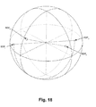
- Fig. 19 to 21 show a Poincare sphere, wherein the retardation device is a half wave plate with the polarization eigenstates SOP f , SOP s being aligned along the S3 axis corresponding to left- and right handed circular polarization states.
- the input polarization state SOP i is on a great circle including the S1 and S3 axes.
- the output polarization state SOP o is located on the Poincare sphere corresponding to a 180°-rotation from the input polarization state SOP ⁇ around a connection line between the center of the Poincare sphere and the polarization eigenstate SOP f .
- the rotation axis matches with the S3 axis corresponding to a half wave rotator.
- the input polarization state SOP i is located where the positive S1 axis intersects the Poincare sphere.
- the output polarization state SOP o is located where the negative S1 axis intersects the Poincare sphere.
- the relative orientation between the input polarization state SOP o and the polarization eigenstate SOP f is 90°, corresponding to 45° (i.e. ⁇ /4) in Jones calculus.
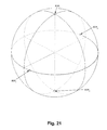
- the input polarization state SOP i is offset from the input polarization state SOP ⁇ of Fig. 20 . More specifically, the input polarization state SOP i of Fig. 21 is shifted toward a position where the positive S2 axis intersects the Poincare sphere. Accordingly, the output polarization state SOP o as shown in Fig. 21 is shifted in the opposite direction in the S1-S2 plane by the same amount.
- the polarization state of light is linear polarized if located on the S1-S2 plane.
- the shift of the polarization states SOP i , SOP o within the S1-S2 plane corresponds to a variation of the respective azimuth angle ⁇ .
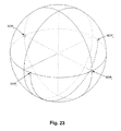
- Fig. 22 and 23 show polarization states SOP ⁇ , SOP o and polarization eigenstates SOP f , SOP s of the retardation device on a Poincare sphere.
- the polarization eigenstate SOP f is 45°-linearly polarized state and is located at the intersection point of the positive S2 axis and the Poincare sphere.
- the input polarization state SOP i is linearly polarized and is located between SOP f and the intersection point of the positive S1 axis and the Poincare sphere.
- the output polarization state SOP o is located at a position on the Poincare sphere corresponding to a 180°-rotation from the input polarization state SOP i around the connection line between the center of the Poincare sphere and SOP f .
- the azimuth angle difference between the input polarization state SOP i and the polarization eigenstate SOP f is 15°.
- the azimuth angle difference between the input polarization state SOP ⁇ and the polarization eigenstate SOP f is 40°.
- the input polarization states SOP i and the output polarization states SOP o of Fig. 22 and 23 are offset from each other in the S1-S2 plane.
- the polarization state of light changes from linear to elliptical and back to linear.
- Fig. 24 to 26 show the polarization states SOP i , SOP o , SOP f , SOP s on a Poincare sphere.
- the input polarization state SOP i and the polarization eigenstate SOP f are the same as in Fig. 23 :
- SOP i and SOP f are linear polarized states with an azimuth angle of 5° and 45°, respectively.
- the retardation device of Fig. 23 is a half wave plate with a retardation of 180°, the retardation is 165° in Fig. 24 , 175° in Fig. 25 , and 185° in Fig. 26 .
- the above described rule for determining the respective output polarization state SOP o applies for retardations other than 180° accordingly.
- the respective output polarization state SOP o of Fig. 24 to 26 is obtained on the Poincare sphere by a rotation from the input polarization state SOP i by the respective angle (165°, 175°, 185°) around the S2 axis, i.e. the SOP f direction. Accordingly, the output polarization states SOP o are located below the S1-S2 plane in Fig. 24 and 25 , while the output polarization state SOP o is located above the S1-S2 plane in Fig. 26 .
- Solid angles corresponding to a closed path over a subset the polarization states SOP ⁇ , SOP o , SOP f , SOP s on the Poincare sphere are associated with differently shaded surfaces in Fig. 24 to 26 .
- the solid angle associated with a first trace SOP i ⁇ SOP 0 ⁇ SOP f is indicated by a darkly shaded area, while a lightly shaded area indicates the solid angle corresponding to a second trace SOPo ⁇ SOP i ⁇ SOP f .
- the first and second traces form the circumference of the darkly shaded area and the lightly shaded area, respectively.
- the border between the darkly shaded and lightly shaded areas is formed by the shortest geodesic arc connecting SOP o and SOP ⁇ on the Poincare sphere.
- the geodesic arc is formed by a great circle on the Poincare sphere which goes through SOP o and SOP i .
- both the first and second traces of Fig. 24 and 25 run counter-clockwise, which means that their corresponding solid angles being mathematically positive.
- the first and second traces of Fig. 26 run clockwise and their corresponding solid angles are mathematically negative.
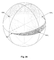
- the input polarization state SOP ⁇ is linearly polarized state with an azimuth angle ⁇ of +5°.
- the polarization eigenstates SOP f , SOP s of the retardation device are linearly polarized states with an azimuth angle ⁇ of +45° and -45°, respectively.
- the relative orientation between the input polarization state SOP i and the polarization eigenstate SOP f is therefore given by an azimuth angle difference of 42.5°.
- the retardation device is a half wave plate with a retardation of approx. 185°. Accordingly, the output polarization state SOP o after passing through the retardation device is located slightly above the S1-S2-plane with an azimuth angle ⁇ of approx. +87.5°.
- the solid angles corresponding to the paths on the Poincare sphere are associated with differently shaded areas.
- the darkly shaded area corresponds to the first trace SOP i ⁇ SOPo ⁇ SOP f . while the lightly shaded area corresponds to the second trace SOPo ⁇ SOP i ⁇ -SOP f .
- the border between the areas is determined by the shortest geodesic arc as described above.
- the relative orientation between the input polarization state SOP i and the polarization eigenstate SOP f can be manipulated, for example, by changing the azimuth angle ⁇ of the input polarization state SOP i and/or the polarization eigenstate SOP f .
- the input polarization state SOP i shown in Fig. 27 is different from Fig. 26 while the polarization eigenstate SOP f remains, or is maintained, constant.
- the change from the SOP i of Fig. 26 to the SOP i of Fig. 27 corresponds to a shift by 10° in the S1-S2-plane toward the negative S2-direction.
- the output polarization state SOP i in Fig. 27 is located slightly above the S1-S2-plane with an azimuth angle ⁇ of approximately -87.5°.
- the solid angles corresponding to the respective paths are indicated with differently shaded areas according to the above description.
- the shaded areas in Fig. 27 show that the solid angle corresponding to the first trace SOP i ⁇ SOP 0 ⁇ SOP f (darkly shaded area) almost covers a full hemisphere, while the solid angle corresponding to the second trace SOP 0 ⁇ SOP i ⁇ SOP f shrinks to a crescent.
- the solid angles corresponding to the first and second traces swap their sizes when the relative orientation between SOP i and SOP f crosses ⁇ /4, assuming that the retardation device has a retardation of 180°, e.g. the retardation device is a half wave plate.
- the retardation device has a retardation of 180°
- the retardation device is a half wave plate.
- the control device can be a processing unit or any other device having a certain processing power.
- the control device may be a computing device.
- the control device can be located remotely from the phase modulation device and connected to it, for example, via a network.
- phase modulation device of the invention uses the phase modulation device of the invention to vary the relative orientation between SOP i and SOP f by as little as 0.02 ⁇ in order to obtain a phase shift of ⁇ , such that the required change in polarization angle is smaller by two orders of magnitude than the affected change in phase angle. Accordingly, the voltages required for inducing the phase shift of ⁇ can be significantly reduced in comparison with the conventional phase modulation devices. The power consumption and/or the time requirement for inducing the phase shift can thereby be reduced using the above described phase modulation device.
- the retardation device includes a birefringent optical device.
- Birefringence refers to the optical property of a medium having a refractive index depending on the polarization and propagation direction of light passing through.
- the birefringence usually is quantified as the maximum difference between refractive indices exhibited by the material. For example, crystals having asymmetric crystal structures or plastics under mechanical stress are often birefringent.
- the delay corresponds to half a wavelength of the input light. Accordingly, the phases of the first and second components of the polarization state are shifted with respect to each other resulting in a phase difference of ⁇ .
- the output polarization state SOP o is rotated with respect to the input polarization state SOPi; with both polarization states SOP ⁇ , SOP o being linear polarization states.
- the input polarization state is rotated around one of the optic axes of the retardation device by 180°.
- the retardation device comprises a half wave plate.
- a "wave plate” refers to an optical device or element that transforms the SOP of the input light to a polarization state of the output light, SOP o , by either changing the amplitude ratio between the first and second components and/or by delaying one of the first and second components in comparison with the other.
- Each wave plate has two polarization eigenstates SOP f and SOP s corresponding to a fast and slow axis with the respective azimuth angles ⁇ f and ⁇ s .
- the half wave plate can comprise a birefringent material, such as quartz or mica.
- the half wave plate has a predetermined thickness as a function of the wavelength of the light and the difference of the refractive index.
- control device is configured to manipulate the polarization state SOP i of the input light.
- the manipulation of the polarization state SOP ⁇ generally refers to altering the azimuth angle and/or the ellipticity of the polarization state SOP i of the input light.
- a linear polarization state SOP i can be turned into a different linear polarization state.
- a linear, circular or elliptical polarization state SOP i can be transformed into any other of linear, circular or elliptical polarization state.
- the control device can be configured to rotate the polarization plane of the input light.
- control device is configured to manipulate the polarization eigenstates SOP f , SOP s of said retardation device.
- the manipulation may change the azimuth angle and/or the ellipticity of the respective polarization eigenstate SOP f , SOP s .
- the azimuth angle of the retardation device may be changed simply by rotating the retardation device. Accordingly, the retardation device can be rotated around an axis parallel to the propagation direction of the input light. In particular, the retardation device may be rotated such that the azimuth angle ⁇ f and ⁇ s of one of the polarization eigenstates SOP f , SOP s is varied around ⁇ /4 from the input azimuth angle ⁇ i .
- the azimuth angle of the retardation device may be changed by exploiting electro-optical properties of or inducing a thermal stress to a birefringent medium of the retardation device.
- control device is configured to change the angle between the polarization state SOP i of the input light and one of the polarization eigenstates SOP f , SOP s from an angle below ⁇ /4 to an angle above ⁇ /4 and/or vice versa.
- the loss factors ⁇ f and ⁇ s obtained from the Jones matrix of the retardation device are equal or nearly equal. If the loss factors differ from each other, the angle variation may be performed by the same absolute amount, however with respect to an angle that is offset from ⁇ /4.
- an angle between the polarization state SOP i of the input light and one of the polarization eigenstates SOP f , SOP s of the retardation device is 90° on the Poincare sphere, corresponding to 45° in the Jones calculus.
- control device is configured to manipulate an optical path length covered by light while passing through the retardation device.
- the optical path length refers to a product of a geometric path length covered by the light in the retardation device and the corresponding refractive index.
- the geometric path length covered by the light is varied.
- the geometric path length can be varied by changing a thickness of a part of the retardation device which is penetrated by the light.
- the geometric light path may refer to a distance between a first position where the light enters the retardation device and a second position where the light exits the retardation device when the light propagates along a straight line. If the retardation device comprises a birefringent medium and/or a half wave plate, the length can refer to a corresponding distance in that birefringent medium or half wave plate.
- the obtained phase shift is caused by a geometrical phase shift effect.
- the geometrical phase shift refers to ⁇ geo as explained above.
- the above mentioned predetermined angle range is ⁇ /4 ⁇ 10%, preferably ⁇ /4 ⁇ 5% and most preferably ⁇ /4 ⁇ 2%.
- the polarization states SOP i , SOP f and SOP s are expressed by complex two dimensional Jones vectors.
- the dot (•) represents the complex dot product.
- a first loss factor ⁇ f and a second loss factor ⁇ s corresponding to the first and second polarization eigenstates SOP f , SOP s , respectively, are equal or differ from each other by 5% or less. If the difference between the loss factors ⁇ f and ⁇ s is larger, a reference angle, here ⁇ /4, may be shifted.
- the above described scheme for inducing the phase shift of ⁇ is not limited to a certain wavelength range, i.e. the input light may have any wavelength available.
- the wavelength of the input light is between 1•10 -6 m to 2•10 -6 m corresponding to conventional wavelength ranges in the optical communication.
- the input light is provided in a wavelength range within the C band, S band or L band as defined in the optical communication.
- the input light can be referred to as a carrier signal in terms of the optical communication.
- the input light may correspond to an electromagnetic signal in typical wavelength range employed in optical communication.
- a receiver for receiving a light signal, which is modulated with respect to its polarization comprises a retardation device characterized by first polarization eigenstate SOP f and second polarization eigenstates SOP s .
- Light polarized according to the second polarization eigenstate SOP s acquires, upon passing through the retardation device, a delay with regard to light polarized according to the first polarization eigenstate SOP f , which delay corresponds to ⁇ /2 ⁇ 30%, preferably ⁇ /2 ⁇ 20% and most preferably ⁇ /2 ⁇ 10%.
- the retardation device is arranged to receive input light having a polarization state SOP i that defines an angle with respect to one of the first polarization eigenstate SOP f and second polarization eigenstate SOP s within a predetermined angle range.
- said predetermined angle range is ⁇ /4 ⁇ 10%, preferably ⁇ /4 5% and most preferably ⁇ /4 ⁇ 2%.
- the polarization states SOP ⁇ , SOP f and SOP s are expressed by complex two dimensional Jones vectors.
- the dot (•) represents the complex dot product.
- the azimuth angle of the polarization states SOP i , SOP f and/or SOP s may be varied within a small range, for example ⁇ 10°, preferably ⁇ 5° and most preferably ⁇ 2°, around the reference angle difference of ⁇ /4, assuming that the first loss factor ⁇ f and the second loss factor ⁇ s corresponding to the first and second polarization eigenstates SOP f , SOP s , respectively, are equal or differ from each other by 5% or less. If the difference between the loss factors ⁇ f and ⁇ s is larger, the reference angle may be shifted from ⁇ /4.
- the receiver may be provided with a retardation device of one of the types recited above with reference to the modulation device.
- Providing the retardation device at the receiver rather than at the transmitter viz. its associated modulation device have the advantage that transmission errors, for example due to polarization crosstalk effects for long transmission distances, can be reduced because the transmitted signal carries only small variations of the polarization state instead of a phase shifts of ⁇ .
- the receiver comprises a control device for adjusting the polarization eigenstates SOP f , SOP s of said retardation device such that a change in the polarization state SOP ⁇ of the received light signal due to said polarization modulation leads to a phase shift of ⁇ ⁇ 30%, preferably ⁇ ⁇ 20% and most preferably ⁇ ⁇ 10% of the output light of said retardation device.
- the control device can be configured to maintain a predetermined azimuth angle difference between one of the polarization eigenstates SOP f , SOP s of the retardation device and a reference polarization state.
- This reference polarization state could e.g. be the average of the different SOP i , i.e. the input polarization states after acquiring different polarization modulations for generating the phase shift of ⁇ , or any other suitable reference polarization state.
- the input azimuth angle ⁇ i and/or one or both of the azimuth angles ⁇ f , ⁇ s is altered around the predetermined angle difference.
- the predetermined angle difference is 45°.
- the azimuth angle difference between the input polarization state SOP i and the respective polarization eigenstate (or optic axis of a birefringent medium) SOP f , SOP s can also referred to as orientation angle.
- control device is configured for adjusting the polarization eigenstates SOP f , SOP s by rotating said retardation device.
- the control device is configured to rotate the birefringent medium or the half wave plate relative to the propagation direction of the input light.
- a transmitter comprising the above described phase modulation device.
- a phase modulating method comprises the steps of:
- the phase modulation device may receive the input light as a carrier signal and impose phase shifts of ⁇ according to the modulation signal to be transmitted with the carrier signal.
- the angle difference between the input azimuth angle ⁇ i of the input polarization state SOP i and one or both of the azimuth angles ⁇ f , ⁇ s of the polarization eigenstates SOP t , SOP s is varied around the predetermined angle difference.
- the amount of delay acquired by the light upon passing through the retardation device is varied.
- the angle difference in azimuth may be varied within a small range, for example ⁇ 10°, preferably ⁇ 5° and most preferably ⁇ 2°, around a reference angle difference of ⁇ /4, assuming that the first loss factor ⁇ f and the second loss factor ⁇ s , corresponding to the first and second polarization eigenstates SOP f , SOP s , respectively, are equal or differ from each other by 5% or less. If the difference between the loss factors ⁇ f and ⁇ s is larger, the reference angle may be shifted from ⁇ /4.
- the above mentioned predetermined angle range is ⁇ /4 ⁇ 10%, preferably ⁇ /4 ⁇ 5% and most preferably ⁇ /4 ⁇ 2%.
- the polarization states SOP f and SOP i are expressed by complex two dimensional Jones vectors.
- the dot (•) represents the complex dot product.
- the voltages required for inducing the phase shift of ⁇ can be significantly reduced in comparison with conventional phase modulation methods.
- the power consumption and/or the time requirement for inducing the phase shift can thereby be reduced using the above described phase modulation device.
- the step of controlling the angle includes rotating the polarization state SOP i of the input light relative to the polarization eigenstates SOP f , SOP s of the retardation device.
- the input polarization state SOP i is rotated around an axis parallel to the propagation direction of the input light.
- the rotation of the input polarization state SOP ⁇ is performed within a range of 0.1 ⁇ , preferably 0.05 ⁇ and most preferably 0.02 ⁇ above and below the predetermined azimuth angle as described above.
- the step of controlling the angle includes rotating the retardation device relative to the polarization state SOP ⁇ of the input light.
- the retardation device can include a birefringent device, in particular a half wave plate.
- the retardation device may be rotated around an axis parallel to the propagation direction of the input light.
- the step of controlling the amount of said delay upon passing through said retardation device includes manipulating a length covered by light while passing through the retardation device.
- the length covered by light can be manipulated, for example, by exploiting piezoelectric, electro-optical or thermal properties of a birefringent medium.
- an electric motor, a piezoelectric device, an optoelectronic device or a combination thereof can be employed to manipulate the respective retardation device.
- Such manipulation or modulation comprise, for example, rotating the retardation device, adjusting an offset angle, switching between different light paths, altering the optic axes, etc.
- the half wave plates as will be described later, can be realized by a LiNbO3 electro-optical modulator.
- Fig. 1 shows a schematic view of a first embodiment of a phase modulation device 10.
- the phase modulation device 10 comprises a retardation device 12 and a control device 14 communicatively coupled to each other.
- a light source 16 generates an input light L i having a defined frequency and defined amplitude.
- the input light L i is a laser signal and the light source is a laser light source.
- the input light L i is polarized and has an input polarization state SOP i .
- the electromagnetic fields of the input light L i oscillates in planes perpendicular to its propagation direction.
- the SOP ⁇ can generally be elliptical having an ellipticity ⁇ i ⁇ 0 and an azimuth angle ⁇ i ⁇ 0.
- the SOP i of the input light L i is linear.
- angle and “angle difference" of polarization states refer to the respective azimuth angle, unless indicated otherwise.
- the retardation device 12 receives the input light L i from the light source 16.
- the retardation device 12 has a first polarization eigenstate SOP f and a second polarization eigenstate SOP s .
- Light propagating in the retardation device experiences different refractive indices along the polarization eigenstates SOP f and SOP s .
- the polarization eigenstates SOP f , SOP s are also referred to as ordinary and extraordinary optic axes of the birefringent retardation device 12.
- the first and second polarization eigenstates SOP f , SOP s are elliptical.
- the first polarization eigenstate SOP f and the second polarization eigenstate SOP s correspond to the fast axis and slow axis of the retardation device 12, respectively.
- the polarization eigenstates SOP f , SOP s are linear.
- Light propagating in the retardation device 12 is divided to a first light component L f and a second light component L s corresponding to a projection of the polarization state of the light on the first polarization eigenstate SOP f and on the second polarization eigenstate SOP s , respectively.
- the first and second light components L f , L s experience different refractive indices according to the fast and slow axes SOP f , SOP s .
- the second light component L s acquires a delay with respect to the first light component L f .
- the phase of the electromagnetic fields according to the first and second components L f , L s are shifted with respect to each other.
- the amplitudes of both components L f , L s change differently while propagating in the retardation device 12.
- the second light component L s being aligned with the slow optic axis SOP s of the retardation device 12, acquires a delay of about half the wavelength ⁇ , of the light with respect to the first light component L f .
- the delay amounts to ⁇ /2 ⁇ 30%, preferably ⁇ ⁇ 20% and most preferably ⁇ /2 ⁇ 10%.
- the phase of the second light component L s is shifted by ⁇ or approximately ⁇ with respect to the first light component L f .
- the polarization state of the light propagating in the retardation device 12 is rotated.
- the azimuth angle of the rotation is twice the difference in azimuth angle between the input polarization state SOP ⁇ and the respective polarization eigenstate SOP f , SOP s . Accordingly, if the azimuth angle difference ⁇ is 45°, the resulting rotation of the polarization state equals 90°.
- the retardation device 12, the light source 16 and the optic fiber connecting the same are arranged such that the input polarization state SOP i is tilted by about ⁇ /4 ⁇ 10%, preferably ⁇ /4 5% and more preferably ⁇ /4 ⁇ 2%, with respect to the first polarization eigenstate SOP f of the retardation device 12 when received by the retardation device 12.
- Light exiting the retardation device 12 after passing through is referred to as output light L o .
- the output light L o has an output polarization state SOP o that is rotated around the input polarization state SOP i by about ⁇ .
- the control device 14 performs at least one of the following actions:
- the delay of the retardation device 12 is adjusted to correspond to precisely ⁇ /2, and the angle difference ⁇ is changed from a value infinitesimally below 45° to a value infinitesimally above 45°, the resultant phase shift corresponds to precisely ⁇ .
- the angle difference ⁇ is kept at 45° and the delay of the retardation device 12 is changed from a value infinitesimally below ⁇ /2 to a value infinitesimally above ⁇ /2, the resulting phase shift likewise corresponds to precisely ⁇ .
- embodiments of the invention are not limited to this scenario. Instead, it is possible that both, the delay and the angle difference change at the same time. Moreover, it is possible that the changes are not infinitesimal, and the delay does need not to precisely correspond to ⁇ /2.
- the output polarization state SOP o of the output light L o can be imposed with a phase shift of ⁇ or at least nearly ⁇ according to a modulation signal by means of said control device.
- each phase shift of ⁇ could refer to a "1" in terms of a binary modulation signal.
- predetermined numbers of consecutive phase shifts of ⁇ are respectively associated with a respective value.
- eight consecutive periods of oscillation can be grouped to a byte.
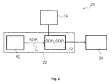
- Fig. 2 shows a schematic view of a second embodiment of a phase modulation device 20.
- the phase modulation device 20 has basically the same structure and elements as the phase modulation device 10 of Fig. 1 .
- the phase modulation device 20 differs from the phase modulation device 10 in that the light source 16 and the retardation device 12 are provided within an integrated photonic circuit 22.
- the output light L o having the output polarization state SOP o is emitted by the integrated photonic circuit 22 and transmitted via a transmission link to a receiver 24.
- the transmission link 24 receives the output light SOP o carrying a phase modulated signal imposed with one or more phase shifts of ⁇ .
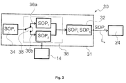
- Fig. 3 shows a schematic view of a third embodiment of a phase modulation device 30.
- the retardation device of the phase modulation device 30 is embodied by a birefringent optical device.
- the birefringent optical device is a half wave plate 32 having a fast axis SOP f and a slow axis SOP s .
- both optic axes SOP f , SOP s are linear axes in the laboratory system.
- the phase modulation device 30 comprises a laser beam source 34 which generates a monochromatic laser beam L i as the input light.
- the laser beam L i is linearly polarized with an azimuth angle ⁇ i .
- the half wave plate 32 is arranged such that the relative orientation of the fast and slow optic axes SOP f , SOP s with respect to the input polarization state SOP i is within a predetermined range.
- a polarization controller 36 is connected in series between the half wave plate 32 and the laser light source 34.
- the polarization controller 36 selectively transforms the input polarization state SOP i into one of two different polarization states SOP i and SOP 2 .
- the first polarization state SOP 1 is offset from the fast polarization axis SOP f by ⁇ /4 + ⁇ 1
- the second polarization state SOP 2 is offset from SOP f by ⁇ /4 - ⁇ 2 .
- Both ⁇ 1 ⁇ f and ⁇ 2 are angular offsets smaller than 0.1 ⁇ , pref erably smaller than 0.05 ⁇ and more preferably smaller than 0.02 ⁇ .
- the polarization controller 36 comprises two polarization branches 36a, 36b that can be selectively connected to the laser light source 34 and the half wave plate 32.
- a switching unit 38 switches between the two polarization branches 36a, 36b according to the modulation signal which is to be imposed to the laser beam L i .
- the polarization state SOP i or SOP 2 is divided into two light components L f and L s according to the optic axes SOP f and SOP s of the half wave plate 32, as described above.
- the slow light component L s acquires a delay with respect to the fast light component L f , resulting in a rotation of the azimuth angle ⁇ 0 of the output light L o .
- the half wave plate 32, the laser light source 34 and the polarization controller 36 are implemented in an integrated photonic circuit 31.
- the laser beam L i from the laser light source 34 propagates via one or more waveguides in the integrated photonic circuit 31.
- further waveguides and optical elements such as a collimator, a lens, an aperture, a mirror, a waveguide coupler, a splitter, another modulator or a combination thereof, may be arranged in the respective integrated photonic circuit.
- the control device 14 is electrically or communicatively connected to the polarization controller 36.
- the control device 14 receives the modulation signal and decides which one of the two polarization branches 36a, 36b is to be connected to the laser light source 34 according to the modulation signal. As described above, the action of the control device 14 results in a phase shift of ⁇ or approximately ⁇ imposed on the output polarization state SOP o of the output light SOPo .
- the switching unit 38 is provided between the outputs of the polarization branches 36a, 36b and the half wave plate 32.
- the additional switching unit selectively connects one of the polarization branches 36a, 36b with the half wave plate 32 according to the modulation signal.
- the switching unit 38 is provided at the input side as well as at the output side of the polarization branches 36a, 36b.
- the output light SOP o carrying the modulation signal imposed as phase shifts of ⁇ is transmitted from the integrated photonic circuit 31 via the transmission link to a receiver 24 as described above.
- Fig. 4 shows a schematic view of a fourth embodiment of a phase modulation device 40.
- the phase modulation device 40 comprises a first half wave plate 42 with fast and slow axes SOP f , SOP s and a second half wave plate 44 with fast and slow axes SOP' f , SOP' s .
- the first and second half wave plates 42, 44 are arranged such that their respective fast axes SOP' f , SOP' f are offset by ⁇ /4 + ⁇ 1 and by ⁇ /4 - ⁇ 2 with respect to SOP j , wherein both ⁇ 1 and ⁇ 2 are positive numbers less than 0.1 ⁇ , preferably 0.05 ⁇ and most preferably 0.02 ⁇ .
- the half wave plates are of the same geometry and made of the same material such that the amount of the dynamic phase shift imposed on the light passing through both of the half wave plates 42, 44 is the same.
- a phase shift of ⁇ is imposed to the output polarization state SOP o due to the geometric phase shift.
- the switching unit 38 selectively connects the laser light source 34 with one of the half wave plates 42, 44 according to the modulation signal.
- the control device 14 (not shown in Fig. 4 ) can be connected to the switching unit 38 to receive the modulation signal and control the switching unit 38 accordingly.
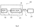
- Fig. 5 shows a schematic view of a fifth embodiment of a phase modulation device 50.
- a half wave plate 52 is connected to a laser light source 16.
- the half wave plate 52 is rotatable within an angle range of ⁇ 0.1 ⁇ , preferably ⁇ 0.05 ⁇ and most preferably ⁇ 0.02 ⁇ with respect to an offset angle of ⁇ /4 from the input polarization state SOP ⁇ of the input light L i .
- a phase shift of ⁇ ⁇ 30%, preferably ⁇ ⁇ 20% and most preferably ⁇ ⁇ 10% due to the geometric phase shift is imposed on the output polarization state SOPo .
- An electric motor or a piezoelectric device (not shown) can be used to rotate the half wave plate 52 according to the modulation signal.
- the control device 14 (not shown in Fig. 5 ) can be connected to the half wave plate 52 or the electric motor or the piezoelectric device for controlling the angular offset between the fast axis of the half wave plate 52 and the input polarization state SOP ⁇ .
- the geometric phase shift of ⁇ can be obtained by altering the amount of the delay acquired by light upon passing through the retardation device.
- different mechanisms or techniques can be employed to alter the amount of the delay.
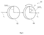
- Fig. 6 shows a schematic partial view of a first embodiment of a retardation device 60.
- the retardation device 60 comprises two cascaded linear wave plates 62, 64 arranged parallel to each other.
- a first wave plate 62 has a first fast axis SOP f1 .
- a second wave plate 64 has a second fast axis SOP f2 .
- the first and second fast axes SOP f1 , SOP f2 are offset from each other by an angle ⁇ .
- the first and second wave plates 62, 64 are wave plates each having a retardation of greater than ⁇ /2.
- the geometric phase shift of ⁇ can be induced by rotating at least one of the first and second wave plates 62, 64 with respect to each other within a range corresponding to an acquired delay of ⁇ 0.5 ⁇ , preferably ⁇ 0.2 ⁇ and most preferably ⁇ 0.1 ⁇ .
- Fig. 7 shows a schematic partial view of a second embodiment of a retardation device 70.
- the retardation device 70 comprises two wave plates 72, 74 shaped as complementary wedges.
- the wave plates 72, 74 are above mentioned wave plates.
- One or both of the wave plates 72, 74 can be moved perpendicular to the propagation direction of the input light L i . A length covered by the light passing through the moved wave plate 72, 74 changes, thereby altering the amount of delay acquired by the light.
- the geometric phase shift of ⁇ can be induced by moving at least one of the first and second wave plates 72, 74 perpendicular to the propagation direction of the light within a range corresponding to an acquired delay of ⁇ 0.5 ⁇ , preferably ⁇ 0.2 ⁇ . and most preferably ⁇ 0.1 ⁇ .
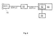
- Fig. 8 shows a schematic view of a first embodiment of a receiver 80 comprising a retardation device 82.
- the laser light source 16 generates and emits a laser light as the input light L i as described above.
- the light source 16 is rotated according to the modulation signal by an azimuth angle ⁇ of less than 0.02 ⁇ .
- the optic fiber is twisted at a position between the light source 16 in order to rotate the input light L i .
- the input light L i is received by a transmission link 84 which transmits the input light L i to the receiver 80.
- the retardation device 82 comprises a half wave plate having a fast axis SOP f arranged offset by 45° from the incident input polarization SOP i .
- a control device 86 compensates fluctuations of the input polarization SOP i ⁇ , for example due to environmental instabilities, and adjusts the orientation of the half wave plate 82.
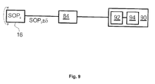
- Fig. 9 shows a schematic view of a second embodiment of a receiver 90 comprising a retardation device.
- the laser light source 16 generates and emits the laser input light L i as described above.
- the light source 16 is rotatable and the input light L i is modulated with respect to its polarization by an azimuth angle ⁇ as described above.
- the input light L i is then transmitted via the transmission link 84 to the receiver 90.
- the receiver 90 comprises a polarization controller 92 and a half wave plate 94.
- the polarization controller 92 is arranged at a predetermined orientation with respect to the fast axis SOP f of the half wave plate 94.
- the polarization controller 92 is configured to recognize the polarization state SOP i of the received input light L i and convert the polarization state of light transmitted to the half wave plate 94 relatively to the fast axis SOP f of the half wave plate 94.
- the variation of the polarization state SOP i of the input light L i received by the polarization controller 92 can differ from or be equal to the variation of the polarization state of the light transmitted to the half wave plate 94.
- a signal carrying relatively small polarization modulation is transmitted to the receiver 80, 90.
- the phase shift of ⁇ or approximately ⁇ is obtained at the receiver after the received light passes through the retardation device comprised by the receiver 80, 90. This way, transmission errors can be reduced due to the relatively small difference in polarization states corresponding to different values.
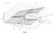
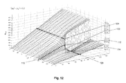
- Fig. 10 to 15 show each a diagram of the total phase ⁇ tot resulting from passing through a half wave plate as a function of the acquired retardation ⁇ and the negative cosine -p of twice the relative orientation between the input polarization state SOP i and the polarization eigenstate SOP f of the half wave plate.
- the relative orientation refers not only to the azimuth angle difference ⁇ but generally to an angle difference in the Jones calculus.
- ⁇ equaling zero corresponds to a relative orientation of 45°.
- the cosine function continuously declines from +1 to -1 corresponding to an increase of the relative orientation from 0° to 90°.
- the retardation ⁇ in particular indicates the acquired delay between the light components upon passing through the half wave plate.
- the total phase ⁇ tot refers to the total phase change the light acquires upon passing through the half wave plate.
- the cosine ⁇ is also referred to as the relative orientation, as appropriate, for the sake of simplicity.
- the steep step corresponds to the above describes geometric phase shift.
- a phase shift of ⁇ (or approximately ⁇ ) can be obtained, for example, by changing the retardation ⁇ over 180° while keeping the relative orientation ⁇ at 45° or vice versa.
- a first path 110 and a second path 120 can be defined which are representative for obtaining the phase shift of ⁇ (or approximately ⁇ ) originating from the geometric phase shift.
- the respective first and second paths 110, 120 are shown as bullets interconnected by a thick line.
- the first path 110 corresponds to changing the retardation ⁇ from below 180° to above 180° or vice versa, while the relative orientation ⁇ is fixed at 45°.
- the second path 120 corresponds to changing the relative orientation ⁇ from below 45° to above 45° or vice versa, while the retardation ⁇ is fixed at 180°.
- coordinates 112, 114, 122, 124 corresponding to positions in an immediate vicinity of the steep step are indicated.
- the coordinates 112, 114, 122, 124 are indicative of respective positions along the first and second paths 110, 120 immediately before and after the phase shift of ⁇ (or approximately ⁇ ).
- the coordinates 112, 114 differ in the retardation ⁇ of 175° and 185°.
- the total phase ⁇ tot decreases from 175° to 1° when changing the coordinates from 112 to 114, resulting in a phase shift of 174° corresponding to 0.97 ⁇ .
- the first coordinates 122 have a relative orientation ⁇ of slightly below 0, while the second coordinates 124 have a relative orientation ⁇ of slightly above 0.
- the total phase ⁇ tot increases from 90° to 266° when changing the coordinates from 122 to 124, resulting in a phase shift of 0.98 ⁇ .
- the changes of the retardation ⁇ and the relative orientation ⁇ may be combined in order to obtain the phase shift of ⁇ (or approximately ⁇ ).
- the phase shift of ⁇ (or approximately ⁇ ).
- not every path which crosses 180° in retardation ⁇ or 0 in cosine ⁇ on the plane will acquire the phase shift of ⁇ .
- Fig. 10 presents results from simulations assuming that the first and second loss factors ⁇ f , ⁇ s respectively corresponding to the first and second optic axes SOP f , SOP s are equal.
- the loss factors ⁇ f , ⁇ s of a real system may differ from each other.
- the shapes of the geometric phase curves may differ from the diagram shown in Fig. 10 using real half wave plates.
- the phase shift of ⁇ may not occur as steep as shown in Fig. 10 .
- the geometric phase shift may be smaller than ⁇ .
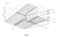
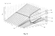
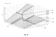
- Fig. 11 to 15 each show simulation results as the ratio ( ⁇ f : ⁇ s ) of the first and second loss factors ⁇ f , ⁇ s is varied.
- the retardation ⁇ axis is displayed on the right side and the cosine - ⁇ axis on the left side. The view angle is therefore rotated around a vertical axis from the diagram of Fig. 10 .
- Fig. 11 the ratio ⁇ f : ⁇ s is 1:1 ⁇ f and the diagram of Fig. 11 therefore shows the same diagram as in Fig. 10 from a different view angle.
- Fig. 12 shows a total phase ⁇ tot diagram, wherein the ratio ⁇ f : ⁇ s is 1:2.
- the steep step is shifted in positive ⁇ -direction (i.e. negative - ⁇ -direction), corresponding to a decrease of the relative orientation.
- the respective positions of the first path 110 and second path 120 are not changed.
- the position and size of the steep step with respect to the retardation ⁇ remains unchanged.
- the steep step is located at ⁇ ⁇ 0.3 corresponding to a relative orientation of approx. 36°.
- the change of the ratio ⁇ f : ⁇ s from 1:1 to 1:2 shifts the steep step by approx. 9° in the negative ⁇ -directions, i.e. at a decreased relative orientation.
- Fig. 13 shows a total phase ⁇ tot diagram, wherein the ratio ⁇ f : ⁇ s is 1:3.
- the steep step is further shifted in positive ⁇ -direction.
- the positions of the first path 110 and the second path 120 are not changed.
- the position and shape of the steep step with respect to the retardation ⁇ remains unchanged.
- the corresponding ⁇ of 0.5 relates to a relative orientation of 30°.
- Fig. 14 shows a total phase ⁇ tot diagram, wherein the ratio ⁇ f : ⁇ s 2:1.
- the steep step is shifted in negative ⁇ -directions (i.e. positive - ⁇ -direction) from the positions shown in Fig. 10 to 13 .
- Fig. 15 shows a total phase ⁇ tot diagram, wherein the ratio ⁇ f : ⁇ s is 3:1.
- the steep step is shifted in negative ⁇ -direction (i.e. positive - ⁇ -direction) even further from the position shown in Fig. 14 .
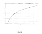
- Fig. 16 shows the calculated relation between the cosine ⁇ corresponding to the steep step and the ratio ⁇ f : ⁇ s of the loss factors.
- the circles represent the numerically calculated values.
- the solid line connects two neighboring values for a better overview.
- the cosine increases continuously with increasing ratio ⁇ f : ⁇ s of the loss factors.
- the ratio of the first loss factor ⁇ f to the second loss factor ⁇ s is, for example, between 0.7:1 and 1:0.7, preferably between 0.8:1 and 1:0.8 and most preferably between 0.9:1 and 1:0.9.
- the steep step is then located at a position with the relative orientation (or the cosine ⁇ ) being changed accordingly.
- phase modulation system in particular incorporating the retardation device or half wave plate as well as the phase modulating method as described above, a relatively small variation in the polarization state can be converted into a relatively large shift in the phase of around ⁇ imposed on a carrier signal.
- phase modulation system and/or retardation device can be combined with either a transmitter or a receiver of an optical communication network as described.
- the energy requirements for phase modulation may be reduced using the phase modulation system and/or the phase modulating method as described. Further, the error rate during the transmission of the carrier signal may be reduced.
Landscapes
- Physics & Mathematics (AREA)
- Optics & Photonics (AREA)
- Engineering & Computer Science (AREA)
- Signal Processing (AREA)
- General Physics & Mathematics (AREA)
- Electromagnetism (AREA)
- Computer Networks & Wireless Communication (AREA)
- Nonlinear Science (AREA)
- Theoretical Computer Science (AREA)
- Polarising Elements (AREA)
Abstract
A phase modulation device is provided that comprises a retardation device and a control device. The retardation device is characterized by first and second polarization eigenstates SOPf and SOPs. Light polarized according to the second polarization eigenstate SOPs acquires, upon passing through said retardation device, a delay with regard to light polarized according to the first polarization eigenstate SOPf, which delay corresponds to λ/2 ± 30%, preferably λ/2 ± 20% and most preferably λ/2 ± 10%. The retardation device is arranged to receive input light having a polarization state SOPi that defines an angle with respect to one of the first and second polarization eigenstates SOPf, SOPs within a predetermined angle range and to emit output light. The control device is configured to control at least one of a change of the angle between the polarization state SOPi of the input light and the respective polarization eigenstate SOPf, SOPs by less than 0.1 *π, preferably less than 0.05*π and most preferably less than 0.02*π; and a change of the amount of said delay upon passing through said retardation device by less than 0.3*λ, preferably less than 0.2*λ and most preferably less than 0.1*λ, such that a phase shift of π ± 30%, preferably π ± 20% and most preferably π ± 10% on the output light is obtained.
Description
- The present invention is in the field of optical data transmission. More specifically, the invention relates to a phase modulation device, a receiver, a transmitter and a phase modulating method.
- Phase modulation refers to a modulation technique that encodes a modulation signal as variations in the instantaneous phase of a carrier wave while the amplitude and the frequency of the carrier wave may remain unaltered.
- A widely used type of phase modulator is an electro-optic modulator which exploits the electro-optic effect, i.e. altering the refractive index of a medium in response to an electric field. A light beam passing through the electro-optic medium can be manipulated as a function of the applied electric field, thereby imposing a modulation on the phase, frequency, amplitude and/or polarization of the light beam.
- Further types of phase modulators include liquid crystal modulators, thermal induction of refractive index changes or length changes e.g. of an optical fiber, and length changes by stretching. Phase modulators are often implemented in integrated optics, where light is modulated in waveguides.
- The electro-optic effect is caused by forces that distort the position, orientation and/or shape of the particles constituting the medium. For example, the refractive index of a lithium niobate crystal changes as a function of the applied electric field, thereby slowing down light travelling through the crystal. The phase of the light exiting the crystal is proportional to the time required for the light to pass through it. The total phase shift may comprise a dynamic and a geometric component.
- The voltage required for inducing a phase change of π is usually called a half-wave voltage. In usual electro-optical phase modulators, the half-wave voltage is several to several tens of volts. Suitable electronic circuits are required for switching the voltage within a small time period, e.g. of few nanoseconds.
- Against this baclcground, a problem underlying the invention is to provide a device and a method for a fast and/or energy efficient phase modulation.
- This problem is solved by a phase modulation device, a receiver, a transmitter as well as a method according to
claim - According to a first aspect of the invention, a phase modulation device is provided that comprises a retardation device and a control device. The retardation device is characterized by first and second polarization eigenstates SOPf and SOPs. Light polarized according to the second polarization eigenstate SOPs acquires, upon passing through said retardation device, a delay with regard to light polarized according to the first polarization eigenstate SOPf, which delay corresponds to λ/2 ± 30%, preferably λ/2 ± 20% and most preferably λ/2 ± 10%. The retardation device is arranged to receive input light having a polarization state SOPi that defines an angle with respect to one of the first and second polarization eigenstates SOPf, SOPs within a predetermined angle range and to emit output light. The control device is configured to control at least one of:
- a change of the angle between the polarization state SOPi of the input light and the respective polarization eigenstate SOPf, SOPs by less than 0.1*π, preferably less than 0.05*π and most preferably less than 0.02*π; and
- a change of the amount of said delay upon passing through said retardation device by less than 0.3*λ, preferably less than 0.2*λ, and most preferably less than 0.1*λ,
- The indication of parameter ranges using "±" refers to all values within the indicated range instead of the boundary values only. For example, the phase shift of π ± 30% refers to all phase shift values from
π 30% to π + 30%. - Accordingly, a phase modulation device is provided that is able to transform a comparatively small change of polarization state of the input light and/or a comparatively small amount of the delay caused by the retardation device into a large phase shift of π or at least close to π imposed on the output light. Accordingly, large phase modulations can be obtained rapidly and with reduced expense of energy.
- As will be explained below, depending on the choice of the angle between the polarization state SOPi of the input light and the respective polarization eigenstate SOPf, SOPs, and further depending on the amount of said delay, in theory, infinitesimally small changes in said angle and/or said delay can lead to changes in the phase of the output light in the amount of π. This will be explained in detail in the following sections. However, in practical applications, a similar effect can be employed with slightly different choices of said angle and said delay, which will make somewhat larger changes in the angle and/or the delay necessary, and which may lead to phase changes that deviate from π by up to ± 10%, up to ± 20% or even up to ± 30%. Nevertheless, even with this "non-optimum" choices of said angle and said delay, a high "leverage", i.e. a high phase change as a result of a small change in angle and/or delay can be achieved.
Next, the principles underlying the phase modulation scheme of the invention shall be explained in detail. - As used herein, the term "light" refers to electromagnetic waves in general and is not limited to visible light. Light travels in a propagation direction and carries oscillating electromagnetic fields. For example, the oscillation takes place in a plane perpendicular to the propagation direction. In addition, the oscillating electromagnetic fields may have a longitudinal component with respect to the propagation direction. The polarization state of light indicates that the tip of the electromagnetic field follows a certain shape when projected onto a plane perpendicular to the propagation direction. Generally, the shape of this light projection is an ellipse.
- The specific shape and orientation of the ellipse is a called a state of polarization (SOP). The SOP can vary or can be changed, e.g. by birefringent elements. For example, the generally elliptical shape of the SOP can degenerate to a line, resulting in a linear SOP, or to a circle, resulting in a circular SOP. The direction in which the tip of the electromagnetic field of a circular SOP moves could be right or left handed with respect to the propagation direction.
- The SOP of an electromagnetic field can be described by two orthogonal polarization components that are defined by two orthogonal laboratory directions x and y, while the propagation direction of the light defines a third laboratory direction z. The directions x, y and z are perpendicular to each other. Each component x and y can be described by three real valued numbers θ, ε and φ as a two dimensional Jones vector

- The angle θ represents an azimuth angle of the SOP and describes the orientation of the long semi-axis of the ellipse relative to the laboratory coordinate system. The angle ε is called ellipticity and defined based on the ratio of the short semi-axis to the long semi-axis of the ellipse. The sign of ellipticity ε indicates the helicity of the electromagnetic field. Accordingly, a SOP can generally be decribed by 8 and ε. The phase φ describes the delay of both x and y components relative to time. The parameters θ, ε and φ can be calculated from the x- and y components of the electromagnetic field.
- The input light passing through the retardation device can be provided by an electromagnetic carrier signal. Usually, the carrier signal is provided as a sinusoidal function of time at a predetermined frequency and amplitude. The phase modulation device basically refers to a device or apparatus configured to encode information inside a carrier signal by imposing phase shifts representing said information. The information is provided as a modulation signal which can generally be any type of function. In binary communication systems, the modulation signal is often provided as a rectangular or gate function. For example, the value "1" corresponds to a change between two amplitude levels of a rectangular modulation function and is imposed as a phase shift of π on the carrier signal. In another example, the value "1" is encoded as a certain number of consecutive phase shifts of π imposed on the carrier signal. Several consecutive wave periods can be merged together to an information unit. For example, a sequence of eight consecutive wave periods forms a byte.
- The phase modulation device may be configured to receive or to generate such a carrier signal. In particular, the phase modulation device can be provided with a light source for generating the carrier signal. The phase modulation device is configured to impose the phase shift of π or at least approximately π on the carrier signal as function of the modulation signal to be transmitted.
- In an example, the retardation device comprises a birefringent medium, e.g. a crystalline glass plate, a section of optic fiber, or a Lithium Niobate (LiNbO3) crystal having two optic axes corresponding to the first and second polarization eigenstates SOPf and SOPs. The term "axis" generally refers to the respective polarization eigenstate which can be elliptical, circular or linear. The light components, which are polarized according to the polarization eigenstates SOPf, SOPs, of light propagating in the birefringent medium experience a first and second refractive index, respectively. The polarization state of light exiting the medium has not changed, if the polarization state is collinear with one of the polarization eigenstates SOPf, SOPs of the retardation device.
- The input light passing through the retardation device can be divided into a first component and a second component corresponding to the projections of the input light onto the first and second polarization eigenstates SOPf, SOPs, respectively. The two components of light passing through the retardation device experience a different refractive index. Without loss of generality, the first polarization eigenstate SOPf can be assumed to be a fast axis associated with a lower refractive index, and the second polarization eigenstate SOPs as the slow axis associated with a higher refractive index. Accordingly, the first component of light propagates faster in the birefringent medium than the second component. If the input polarization state SOP¡ is collinear with one of the polarization eigenstates SOPf, SOPs, the polarization state of an output light, i.e. light exiting the retardation device, is different from the polarization state of the input light.
- The "delay" refers to retardation of one of the first and second light components compared to the other light component while propagating in the retardation device. The phases of the two components shift with respect to each other due to the delay. Also, a total phase of the electromagnetic field of the output light is shifted relative to the total phase which the output light would have upon passing through the same distance in vacuum. The longer the light propagates through the retardation device, the greater becomes said delay. Light passing through the retardation device hence acquires both a change in the polarization state and a phase shift.
- In another example, the retardation device may comprise another means to alter the polarization state of light passing through.
- In addition to the dynamic phase shift, light passing through the retardation device experiences a "geometric phase shift", which is also referred to as Pancharatnam-Berry phase. A more detailed explanation and mathematical discussions are provided by J. C. Gutierrez-Vega, "Pancharatnam-Berry phase of optical systems", .
- Light passing through a birefringent medium can be described within the Jones calculus. For example, the birefringent medium may show no polarization dependent loss (PDL), i.e. loss factors associated with the refractive indices of the birefringent medium may be equal. The input light
E in is transformed toE out upon passing through the birefringent medium, mathematically described by the Jones matrix J as follows:

- The Jones vectors can be transformed to the respective Stokes vectors Qn as follows:

Q n contain three-dimensional, real values. Light passing through a birefringent medium without PDL acquires the following phase shift φ, according to the above cited paper by Gutierrez-Vega:
A the Stokes vector of the polarization state of the input light and Ω XYZ the solid angle corresponding to a surface formed by positions X, Y and Z on a Poincare sphere. φdyn and φgeo respectively correspond to the dynamic and geometric phase shift. For more general cases where the PDL is nonzero, see above mentioned Gutierrez-Vega paper. -
Fig. 17 and18 show each a Poincare sphere which visualizes polarization states in spherical coordinates. According to the Stokes' parametrization of polarization states, the Cartesian axes S1, S2 and S3 correspond to vertical/horizontal linear polarization, ±45° linear polarization and left-/right-hand circular polarization, respectively. Accordingly, polarization states on the equatorial plane, i.e. the S1-S2 plane, are linearly polarized. All the polarization states between the equatorial plane and each of the poles are elliptically polarized, as illustrated inFig. 17 . This description also applies to the Poincare spheres shown inFig. 19 to 28 . - As mentioned above, the polarization state of light is generally elliptical. As shown in
Fig. 17 , the major and minor axes of the ellipse are perpendicular to each other. The ellipticity ε of the polarization state is defined based on the ratio of the semi-axes. The azimuth angle θ indicates the offset angle of the major axis from the S1 axis. On the Poincare sphere and in the Stokes parametrization, both the ellipticity ε and the azimuth angle θ are twice as large as in the Jones calculus, as indicated by "2ε" and "2θ" inFig. 17 . - With reference to
Fig. 18 , the input light has a certain input polarization state SOPi, which is elliptical. The polarization state of light is modified while passing through the retardation device having polarization eigenstates SOPf, SOPs that have a relative orientation with respect to each other. For example, the polarization eigenstates SOPf, SOPs are linearly polarized eigenstates being perpendicular to each other. In another example, the polarization eigenstates SOPf, SOPs are left- and right-handed circular polarization states. In the example shown inFig. 18 , the relative orientation between the polarization eigenstates SOPf, SOPs is 180° on the Poincare sphere, corresponding to a relative orientation of 90° in the Jones calculus. As shown further inFig. 18 , the polarization eigenstates SOPf, SOPs are in general elliptical. - Generally, the retardation device modifies the polarization state of light passing through as a function of, among others, an optical path length, the refractive indices and a relative orientation of the retardation device. As a result, the polarization state of light is converted from the input polarization state SOP¡ to the output polarization state SOPo upon passing through the retardation device.
- If the retardation device is a half wave plate, as schematically shown in
Fig. 18 , the change of the polarization state from SOPi to SOPo corresponds to a counter-clockwise rotation (from a perspective from the outside of the Poincare sphere) of 180° on the Poincare sphere around a rotation axis, which is defined by the direction of SOPf. - In
Fig. 18 to 23 , a trace of the change of the polarization state of light while propagating in the retardation device is visualized by a dotted line connecting SOPi and SOPo. InFig. 18 , the polarization state of light propagating in the retardation device changes from initially elliptical at SOPi over linear when crossing the S1-S2 plane, over differently elliptical on the southern hemisphere, over linear when crossing the S1-S2 plane again, and eventually to elliptical on the northern hemisphere at SOPo. - Herein and in the following, the description refers to the first polarization eigenstate SOPf of the retardation device without loss of generality. It is understood that same or similar effects can be achieved with reference to the second polarization eigenstate SOPs as well.
-
Fig. 19 to 21 show a Poincare sphere, wherein the retardation device is a half wave plate with the polarization eigenstates SOPf, SOPs being aligned along the S3 axis corresponding to left- and right handed circular polarization states. - In
Fig. 19 , the input polarization state SOPi is on a great circle including the S1 and S3 axes. The output polarization state SOPo is located on the Poincare sphere corresponding to a 180°-rotation from the input polarization state SOP¡ around a connection line between the center of the Poincare sphere and the polarization eigenstate SOPf. In the examples shown inFig. 19 to 21 , the rotation axis matches with the S3 axis corresponding to a half wave rotator. - In
Fig. 20 , the input polarization state SOPi is located where the positive S1 axis intersects the Poincare sphere. With the polarization eigenstate SOPf positioned on the S3 axis, the output polarization state SOPo is located where the negative S1 axis intersects the Poincare sphere. The relative orientation between the input polarization state SOPo and the polarization eigenstate SOPf is 90°, corresponding to 45° (i.e. π/4) in Jones calculus. - In
Fig. 21 , the input polarization state SOPi is offset from the input polarization state SOP¡ ofFig. 20 . More specifically, the input polarization state SOPi ofFig. 21 is shifted toward a position where the positive S2 axis intersects the Poincare sphere. Accordingly, the output polarization state SOPo as shown inFig. 21 is shifted in the opposite direction in the S1-S2 plane by the same amount. - As mentioned above, the polarization state of light is linear polarized if located on the S1-S2 plane. Hence, the shift of the polarization states SOPi, SOPo within the S1-S2 plane corresponds to a variation of the respective azimuth angle θ.
-
Fig. 22 and23 show polarization states SOP¡, SOPo and polarization eigenstates SOPf, SOPs of the retardation device on a Poincare sphere. InFig, 22 and23 , the polarization eigenstate SOPf is 45°-linearly polarized state and is located at the intersection point of the positive S2 axis and the Poincare sphere. The input polarization state SOPi is linearly polarized and is located between SOPf and the intersection point of the positive S1 axis and the Poincare sphere. - According to the above described rule, the output polarization state SOPo is located at a position on the Poincare sphere corresponding to a 180°-rotation from the input polarization state SOPi around the connection line between the center of the Poincare sphere and SOPf.
- In
Fig. 22 , the azimuth angle difference between the input polarization state SOPi and the polarization eigenstate SOPf is 15°. InFig. 23 , the azimuth angle difference between the input polarization state SOP¡ and the polarization eigenstate SOPf is 40°. Accordingly, the input polarization states SOPi and the output polarization states SOPo ofFig. 22 and23 are offset from each other in the S1-S2 plane. During the change of the polarization state from SOPi to SOPo (as traced by the dotted line), the polarization state of light changes from linear to elliptical and back to linear. -
Fig. 24 to 26 show the polarization states SOPi, SOPo, SOPf, SOPs on a Poincare sphere. Infig. 24 to 26 , the input polarization state SOPi and the polarization eigenstate SOPf are the same as inFig. 23 : SOPi and SOPf are linear polarized states with an azimuth angle of 5° and 45°, respectively. While the retardation device ofFig. 23 is a half wave plate with a retardation of 180°, the retardation is 165° inFig. 24 , 175° inFig. 25 , and 185° inFig. 26 . - The above described rule for determining the respective output polarization state SOPo applies for retardations other than 180° accordingly. The respective output polarization state SOPo of
Fig. 24 to 26 is obtained on the Poincare sphere by a rotation from the input polarization state SOPi by the respective angle (165°, 175°, 185°) around the S2 axis, i.e. the SOPf direction. Accordingly, the output polarization states SOPo are located below the S1-S2 plane inFig. 24 and25 , while the output polarization state SOPo is located above the S1-S2 plane inFig. 26 . - Solid angles corresponding to a closed path over a subset the polarization states SOP¡, SOPo, SOPf, SOPs on the Poincare sphere are associated with differently shaded surfaces in
Fig. 24 to 26 . Following the mathematical discussions above, the geometric phase shift φgeo is determined by the difference Ω1-Ω2 of the solid angles Ω1=Ω(SOPi-SOPo→SOPf) and Ω2=Ω(SOPo→SOPi-SOPf). - In
Fig. 24 to 26 , the solid angle associated with a first trace SOPi→SOP0→SOPf is indicated by a darkly shaded area, while a lightly shaded area indicates the solid angle corresponding to a second trace SOPo→SOPi→SOPf. The first and second traces form the circumference of the darkly shaded area and the lightly shaded area, respectively. - The border between the darkly shaded and lightly shaded areas is formed by the shortest geodesic arc connecting SOPo and SOP¡ on the Poincare sphere. The geodesic arc is formed by a great circle on the Poincare sphere which goes through SOPo and SOPi.
- In an angle view toward the center of the Poincare sphere from the outside, both the first and second traces of
Fig. 24 and25 run counter-clockwise, which means that their corresponding solid angles being mathematically positive. However, the first and second traces ofFig. 26 run clockwise and their corresponding solid angles are mathematically negative. - When the retardation is below 180° and increases toward 180°, the darkly shaded area having vertex at SOPf decreases and the lightly shaded area having vertex at SOPs grows. When the retardation approaches 180°, and assuming that the loss factors µ1, µ2 are equal, the darkly shaded area is nearly zero and the lightly shaded area reaches almost a full hemisphere, 4π/2 ~ 2π. Both paths associated with the darkly shaded area and the lightly shaded area bear a positive sign. The above described Φ equation therefore yields ∼ π/2.
- When the retardation increases further and exceeds 180°, as shown in
Fig. 26 , the size of both areas remain almost the same, but their respective sign changes from +1 to -1, because the respective traces now run clockwise. The resulting Φ equals -(-π/2) = π/2. Hence, the sign flip causes a shift of the total phase from -π/2 to π/2, resulting in a phase shift of π when crossing 180°. - Another possibility for inducing a phase shift of π is given by changing the relative orientation between the input polarization state SOPi and the polarization eigenstate SOPf (or SOPs) of the retardation device, as will be described in connection with
Fig. 26 and27 . - In
Fig. 26 , the input polarization state SOP¡ is linearly polarized state with an azimuth angle θ of +5°. The polarization eigenstates SOPf, SOPs of the retardation device are linearly polarized states with an azimuth angle θ of +45° and -45°, respectively. The relative orientation between the input polarization state SOPi and the polarization eigenstate SOPf is therefore given by an azimuth angle difference of 42.5°. The retardation device is a half wave plate with a retardation of approx. 185°. Accordingly, the output polarization state SOPo after passing through the retardation device is located slightly above the S1-S2-plane with an azimuth angle θ of approx. +87.5°. - The solid angles corresponding to the paths on the Poincare sphere are associated with differently shaded areas. The darkly shaded area corresponds to the first trace SOPi→SOPo→SOPf. while the lightly shaded area corresponds to the second trace SOPo→SOPi→-SOPf. The border between the areas is determined by the shortest geodesic arc as described above.
- The relative orientation between the input polarization state SOPi and the polarization eigenstate SOPf can be manipulated, for example, by changing the azimuth angle θ of the input polarization state SOPi and/or the polarization eigenstate SOPf. The input polarization state SOPi shown in
Fig. 27 is different fromFig. 26 while the polarization eigenstate SOPf remains, or is maintained, constant. InFig. 27 , the input polarization state SOPi is a linearly polarized state with θ = -5°. The change from the SOPi ofFig. 26 to the SOPi ofFig. 27 corresponds to a shift by 10° in the S1-S2-plane toward the negative S2-direction. - With the polarization eigenstates being at ±45° in the S1-S2-plane, the output polarization state SOPi in
Fig. 27 is located slightly above the S1-S2-plane with an azimuth angle θ of approximately -87.5°. The solid angles corresponding to the respective paths are indicated with differently shaded areas according to the above description. The shaded areas inFig. 27 show that the solid angle corresponding to the first trace SOPi→SOP0→SOPf (darkly shaded area) almost covers a full hemisphere, while the solid angle corresponding to the second trace SOP0→SOPi→ SOPf shrinks to a crescent. - Hence, the solid angles corresponding to the first and second traces swap their sizes when the relative orientation between SOPi and SOPf crosses π/4, assuming that the retardation device has a retardation of 180°, e.g. the retardation device is a half wave plate.
As is seen from the above, in theory it is possible to obtain a large phase shift in the amount of π in response to an infinitesimal change in the initial polarization state, i.e. from SOPi to SOPi Similarly, a large phase shift in the amount of π could also be obtained by an infinitesimal change in the delay associated with the retardation device. The present invention employs this principle to allow for a high "modulation leverage", i.e. a comparatively large change in the phase of the output light of π or at least close to π due to a comparatively small change in the initial polarization state and/or the retardation associated with said retardation device. - The control device can be a processing unit or any other device having a certain processing power. For example, the control device may be a computing device. The control device can be located remotely from the phase modulation device and connected to it, for example, via a network.
- Using prior art equipment, voltage requirements for changing the polarization state by a given polarization angle, and voltage requirements for changing the phase of a carrier signal by a similar amount are typically comparable. In other words, effecting the phase modulation by a polarization modulation does not per se allow for saving energy. However, as is seen from the above, using the phase modulation device of the invention, the relative orientation between SOPi and SOPf is varied by as little as 0.02 π in order to obtain a phase shift of π, such that the required change in polarization angle is smaller by two orders of magnitude than the affected change in phase angle. Accordingly, the voltages required for inducing the phase shift of π can be significantly reduced in comparison with the conventional phase modulation devices. The power consumption and/or the time requirement for inducing the phase shift can thereby be reduced using the above described phase modulation device.
- According to some embodiments, the retardation device includes a birefringent optical device. Birefringence refers to the optical property of a medium having a refractive index depending on the polarization and propagation direction of light passing through. The birefringence usually is quantified as the maximum difference between refractive indices exhibited by the material. For example, crystals having asymmetric crystal structures or plastics under mechanical stress are often birefringent.
- According to some embodiments, the delay corresponds to half a wavelength of the input light. Accordingly, the phases of the first and second components of the polarization state are shifted with respect to each other resulting in a phase difference of π. For example, the output polarization state SOPo is rotated with respect to the input polarization state SOPi; with both polarization states SOP¡, SOPo being linear polarization states. On the Poincare sphere, the input polarization state is rotated around one of the optic axes of the retardation device by 180°.
- According to some embodiments, the retardation device comprises a half wave plate.
- As used here, a "wave plate" refers to an optical device or element that transforms the SOP of the input light to a polarization state of the output light, SOPo, by either changing the amplitude ratio between the first and second components and/or by delaying one of the first and second components in comparison with the other. Each wave plate has two polarization eigenstates SOPf and SOPs corresponding to a fast and slow axis with the respective azimuth angles θf and θs. The wave plate has a certain optical length and can introduce different delays δf, δs for the polarization components according to its fast and slow axis, respectively. The difference of these delays Δδ = δf - δs can be referred to as the birefringence of the wave plate.
- In case that the PDL is nonzero, the intensity of SOPo may vary depending on which of SOPf, SOP¡ the SOPi is aligned to. (Elliptizität = 0]
- The half wave plate can comprise a birefringent material, such as quartz or mica. The half wave plate has a predetermined thickness as a function of the wavelength of the light and the difference of the refractive index.
- According to some embodiments, the control device is configured to manipulate the polarization state SOPi of the input light.
- The manipulation of the polarization state SOP¡ generally refers to altering the azimuth angle and/or the ellipticity of the polarization state SOPi of the input light. For example, a linear polarization state SOPi can be turned into a different linear polarization state. Further, a linear, circular or elliptical polarization state SOPi can be transformed into any other of linear, circular or elliptical polarization state. For this purpose, the control device can be configured to rotate the polarization plane of the input light.
- According to some embodiments, the control device is configured to manipulate the polarization eigenstates SOPf, SOPs of said retardation device.
- In particular, the manipulation may change the azimuth angle and/or the ellipticity of the respective polarization eigenstate SOPf, SOPs. For example, the azimuth angle of the retardation device may be changed simply by rotating the retardation device. Accordingly, the retardation device can be rotated around an axis parallel to the propagation direction of the input light. In particular, the retardation device may be rotated such that the azimuth angle θf and θs of one of the polarization eigenstates SOPf, SOPs is varied around π/4 from the input azimuth angle θi.
- In other examples, the azimuth angle of the retardation device may be changed by exploiting electro-optical properties of or inducing a thermal stress to a birefringent medium of the retardation device.
- According to some embodiments, the control device is configured to change the angle between the polarization state SOPi of the input light and one of the polarization eigenstates SOPf, SOPs from an angle below π/4 to an angle above π/4 and/or vice versa.
- In particular, it is assumed that the loss factors πf and µs obtained from the Jones matrix of the retardation device are equal or nearly equal. If the loss factors differ from each other, the angle variation may be performed by the same absolute amount, however with respect to an angle that is offset from π/4. In order to obtain a reversion of the solid angles as described above, an angle between the polarization state SOPi of the input light and one of the polarization eigenstates SOPf, SOPs of the retardation device is 90° on the Poincare sphere, corresponding to 45° in the Jones calculus.
- According to some embodiments, the control device is configured to manipulate an optical path length covered by light while passing through the retardation device.
- Mathematically, the optical path length refers to a product of a geometric path length covered by the light in the retardation device and the corresponding refractive index. For example, the geometric path length covered by the light is varied. For example, the geometric path length can be varied by changing a thickness of a part of the retardation device which is penetrated by the light. Herein, the geometric light path may refer to a distance between a first position where the light enters the retardation device and a second position where the light exits the retardation device when the light propagates along a straight line. If the retardation device comprises a birefringent medium and/or a half wave plate, the length can refer to a corresponding distance in that birefringent medium or half wave plate.
- According to some embodiments, the obtained phase shift is caused by a geometrical phase shift effect. The geometrical phase shift refers to φgeo as explained above.
- According to some embodiments, the above mentioned predetermined angle range is π/4 ± 10%, preferably π/4 ± 5% and most preferably π/4 ± 2%. The predetermined angle is defined as:

- Herein, the polarization states SOPi, SOPf and SOPs are expressed by complex two dimensional Jones vectors. The dot (•) represents the complex dot product.
- In particular, a first loss factor µf and a second loss factor µs corresponding to the first and second polarization eigenstates SOPf, SOPs, respectively, are equal or differ from each other by 5% or less. If the difference between the loss factors µf and µs is larger, a reference angle, here π/4, may be shifted.
- Generally, the above described scheme for inducing the phase shift of π is not limited to a certain wavelength range, i.e. the input light may have any wavelength available. However, according to some embodiments, the wavelength of the input light is between 1•10-6 m to 2•10-6 m corresponding to conventional wavelength ranges in the optical communication. For example, the input light is provided in a wavelength range within the C band, S band or L band as defined in the optical communication. Furthermore, the input light can be referred to as a carrier signal in terms of the optical communication.
- In particular, the input light may correspond to an electromagnetic signal in typical wavelength range employed in optical communication.
- According to another aspect of the invention, a receiver for receiving a light signal, which is modulated with respect to its polarization is provided. The receiver comprises a retardation device characterized by first polarization eigenstate SOPf and second polarization eigenstates SOPs. Light polarized according to the second polarization eigenstate SOPs acquires, upon passing through the retardation device, a delay with regard to light polarized according to the first polarization eigenstate SOPf, which delay corresponds to λ/2 ± 30%, preferably λ/2 ± 20% and most preferably λ/2 ± 10%. The retardation device is arranged to receive input light having a polarization state SOPi that defines an angle with respect to one of the first polarization eigenstate SOPf and second polarization eigenstate SOPs within a predetermined angle range.
- According to some embodiments, said predetermined angle range is π/4 ± 10%, preferably π/4 5% and most preferably π/4 ± 2%. The predetermined angle is defined as:

- Herein, the polarization states SOP¡, SOPf and SOPs are expressed by complex two dimensional Jones vectors. The dot (•) represents the complex dot product.
- In particular, the azimuth angle of the polarization states SOPi, SOPf and/or SOPs may be varied within a small range, for example ±10°, preferably ±5° and most preferably ±2°, around the reference angle difference of π/4, assuming that the first loss factor µf and the second loss factor µs corresponding to the first and second polarization eigenstates SOPf, SOPs, respectively, are equal or differ from each other by 5% or less. If the difference between the loss factors µf and µs is larger, the reference angle may be shifted from π/4.
- In particular, the receiver may be provided with a retardation device of one of the types recited above with reference to the modulation device. Providing the retardation device at the receiver rather than at the transmitter viz. its associated modulation device have the advantage that transmission errors, for example due to polarization crosstalk effects for long transmission distances, can be reduced because the transmitted signal carries only small variations of the polarization state instead of a phase shifts of π.
- According to some embodiments, the receiver comprises a control device for adjusting the polarization eigenstates SOPf, SOPs of said retardation device such that a change in the polarization state SOP¡ of the received light signal due to said polarization modulation leads to a phase shift of π ± 30%, preferably π ± 20% and most preferably π ± 10% of the output light of said retardation device.
- The control device can be configured to maintain a predetermined azimuth angle difference between one of the polarization eigenstates SOPf, SOPs of the retardation device and a reference polarization state. This reference polarization state could e.g. be the average of the different SOPi, i.e. the input polarization states after acquiring different polarization modulations for generating the phase shift of π, or any other suitable reference polarization state. The input azimuth angle θi and/or one or both of the azimuth angles θf, θs, is altered around the predetermined angle difference. In particular, the predetermined angle difference is 45°. The azimuth angle difference between the input polarization state SOPi and the respective polarization eigenstate (or optic axis of a birefringent medium) SOPf, SOPs can also referred to as orientation angle.
- According to some embodiments, the control device is configured for adjusting the polarization eigenstates SOPf, SOPs by rotating said retardation device.
- If the retardation device comprises a birefringent medium or a half wave plate, the control device is configured to rotate the birefringent medium or the half wave plate relative to the propagation direction of the input light.
- According to a further aspect of the invention, a transmitter is provided comprising the above described phase modulation device.
- According to another aspect of the invention, a phase modulating method is provided. The method comprises the steps of:
- guiding polarized light through a phase modulation device according to one of the embodiments; and
- controlling at least one of:
- a change of the angle between the polarization state SOPi of the input light and one of the polarization eigenstates SOPf, SOPs by less than 0.1*π, preferably 0.05*π and most pref erably 0.02*π, or
- a change of the amount of said delay upon passing through said retardation device by less than 0.5*λ, preferably 0.2*λ and most preferably 0.1*λ,
- In the phase modulation method of the invention, the phase modulation device may receive the input light as a carrier signal and impose phase shifts of π according to the modulation signal to be transmitted with the carrier signal. The angle difference between the input azimuth angle θi of the input polarization state SOPi and one or both of the azimuth angles θf, θs of the polarization eigenstates SOPt, SOPs is varied around the predetermined angle difference. In addition or alternatively, the amount of delay acquired by the light upon passing through the retardation device is varied.
- In particular, the angle difference in azimuth may be varied within a small range, for example ±10°, preferably ±5° and most preferably ±2°, around a reference angle difference of π/4, assuming that the first loss factor θf and the second loss factor µs, corresponding to the first and second polarization eigenstates SOPf, SOPs, respectively, are equal or differ from each other by 5% or less. If the difference between the loss factors µf and µs is larger, the reference angle may be shifted from π/4.
- According to some embodiments, the above mentioned predetermined angle range is π/4 ± 10%, preferably π/4 ± 5% and most preferably π/4 ± 2%. The predetermined angle is defined as:

- Herein, the polarization states SOPf and SOPi are expressed by complex two dimensional Jones vectors. The dot (•) represents the complex dot product.
- Using this method, the voltages required for inducing the phase shift of π can be significantly reduced in comparison with conventional phase modulation methods. The power consumption and/or the time requirement for inducing the phase shift can thereby be reduced using the above described phase modulation device.
- According to some embodiments, the step of controlling the angle includes rotating the polarization state SOPi of the input light relative to the polarization eigenstates SOPf, SOPs of the retardation device.
- In particular, the input polarization state SOPi is rotated around an axis parallel to the propagation direction of the input light. The rotation of the input polarization state SOP¡ is performed within a range of 0.1 π, preferably 0.05 π and most preferably 0.02 π above and below the predetermined azimuth angle as described above.
- According to some embodiments, the step of controlling the angle includes rotating the retardation device relative to the polarization state SOP¡ of the input light.
- The retardation device can include a birefringent device, in particular a half wave plate. The retardation device may be rotated around an axis parallel to the propagation direction of the input light.
- According to some embodiments, the step of controlling the amount of said delay upon passing through said retardation device includes manipulating a length covered by light while passing through the retardation device.
- The length covered by light can be manipulated, for example, by exploiting piezoelectric, electro-optical or thermal properties of a birefringent medium.
-
- Fig. 1
- is a schematic view of a first embodiment of a phase modulation device;
- Fig. 2
- is a schematic view of a second embodiment of a phase modulation device;
- Fig. 3
- is a schematic view of a third embodiment of a phase modulation device;
- Fig. 4
- is a schematic view of a fourth embodiment of a phase modulation device;
- Fig. 5
- is a schematic view of a fifth embodiment of a phase modulation device;
- Fig. 6
- is a schematic view of a first embodiment of a retardation device;
- Fig. 7
- is a schematic view of a second embodiment of a retardation device;
- Fig. 8
- is a schematic view of a first embodiment of a receiver;
- Fig. 9
- is a schematic view of a second embodiment of a receiver;
- Fig. 10
- is a diagram showing the total phase Φtot when a ratio (µf: µs) of the first loss factor µs to the second loss factor µs is 1:1;
- Fig. 11
- is the diagram of
Fig. 10 from another view angle; - Fig. 12
- is a diagram showing the total phase Φtot when the ratio (µf: µs) of the first loss factor µf to the second loss factor µs is 1:2;
- Fig. 13
- is a diagram showing the total phase Φtot when the ratio (µf: µs) of the first loss factor µf to the second loss factor µs is 1:3;
- Fig. 14
- is a diagram showing the total phase Φtot when the ratio (µf: µs) of the first loss factor µf to the second loss factor µs is 2:1;
- Fig. 15
- is a diagram showing the total phase Φtot when the ratio (µf: µs) of the first loss factor µf to the second loss factor µs is 3:1;
- Fig. 16
- is a diagram showing cosine of the relative orientation between the input polarization state and the polarization eigenstate of the retardation device as a function of the the ratio (µf: µs) corresponding to the occurrence of a steep step in the total phase Φtot.;
- Fig. 17
- illustrates the Poincare sphere;
- Fig. 18
- illustrates the change of an input polarization state upon passing through a retardation device by means of a Poincare sphere;
- Fig. 19
- illustrates the change of another input polarization state upon passing through the retardation device of
Fig. 18 by means of a Poincare sphere; - Fig. 20
- illustrates the change of yet another input polarization state upon passing through the retardation device of
Fig. 18 by means of a Poincare sphere; - Fig. 21
- illustrates the change of yet another input polarization state upon passing through the retardation device of
Fig. 18 by means of a Poincare sphere; - Fig. 22
- illustrates the change of yet another input polarization state upon passing through another retardation device by means of a Poincare sphere;
- Fig. 23
- illustrates the change of yet another input polarization state upon passing through the retardation device of
Fig. 22 by means of a Poincare sphere; - Fig. 24
- illustrates traces and the corresponding solid angles on a Poincare sphere;
- Fig. 25
- illustrates further traces and the corresponding solid angles on a Poincare sphere;
- Fig. 26
- illustrates further traces and corresponding solid angles on a Poincare sphere; and
- Fig. 27
- illustrates further traces and the corresponding solid angles on a Poincare sphere.
- For the purposes of promoting an understanding of the principles of the invention, reference will now be made to a preferred embodiment illustrated in the drawings, and specific language will be used to describe the same. It will nevertheless be understood that no limitation of the scope of the invention is thereby intended, such alterations and further modifications in the illustrated apparatus and such further applications of the principles of the invention as illustrated therein being contemplated as would normally occur now or in the future to one skilled in the art to which the invention relates. Same or similar structural or functional features incorporated by different embodiments are indicated by using the same reference numerals in different figures.
- In the following embodiments, an electric motor, a piezoelectric device, an optoelectronic device or a combination thereof can be employed to manipulate the respective retardation device. Such manipulation or modulation comprise, for example, rotating the retardation device, adjusting an offset angle, switching between different light paths, altering the optic axes, etc. In particular, the half wave plates, as will be described later, can be realized by a LiNbO3 electro-optical modulator.
-
Fig. 1 shows a schematic view of a first embodiment of aphase modulation device 10. - The
phase modulation device 10 comprises aretardation device 12 and acontrol device 14 communicatively coupled to each other. Alight source 16 generates an input light Li having a defined frequency and defined amplitude. For example, the input light Li is a laser signal and the light source is a laser light source. The input light Li is polarized and has an input polarization state SOPi. The electromagnetic fields of the input light Li oscillates in planes perpendicular to its propagation direction. The SOP¡ can generally be elliptical having an ellipticity εi≠0 and an azimuth angle θi≠0. For the sake of simplicity, it is assumed that the SOPi of the input light Li is linear. In the following, "angle" and "angle difference" of polarization states refer to the respective azimuth angle, unless indicated otherwise. - The
retardation device 12 receives the input light Li from thelight source 16. Theretardation device 12 has a first polarization eigenstate SOPf and a second polarization eigenstate SOPs. Light propagating in the retardation device experiences different refractive indices along the polarization eigenstates SOPf and SOPs. The polarization eigenstates SOPf, SOPs are also referred to as ordinary and extraordinary optic axes of thebirefringent retardation device 12. Generally, the first and second polarization eigenstates SOPf, SOPs are elliptical.
Without loss of generality, the first polarization eigenstate SOPf and the second polarization eigenstate SOPs correspond to the fast axis and slow axis of theretardation device 12, respectively. For the sake of simplicity, it is assumed that the polarization eigenstates SOPf, SOPs are linear. Light propagating in theretardation device 12 is divided to a first light component Lf and a second light component Ls corresponding to a projection of the polarization state of the light on the first polarization eigenstate SOPf and on the second polarization eigenstate SOPs, respectively. While propagating in theretardation device 12, the first and second light components Lf, Ls experience different refractive indices according to the fast and slow axes SOPf, SOPs. As a result, the second light component Ls acquires a delay with respect to the first light component Lf. Accordingly, the phase of the electromagnetic fields according to the first and second components Lf, Ls are shifted with respect to each other. Optionally, the amplitudes of both components Lf, Ls change differently while propagating in theretardation device 12. - More specifically, the second light component Ls, being aligned with the slow optic axis SOPs of the
retardation device 12, acquires a delay of about half the wavelength λ, of the light with respect to the first light component Lf. For example, the delay amounts to λ/2 ± 30%, preferably λ ± 20% and most preferably λ/2 ± 10%. Accordingly, the phase of the second light component Ls is shifted by π or approximately π with respect to the first light component Lf. - As a result of the different delays acquired, the polarization state of the light propagating in the
retardation device 12 is rotated. The azimuth angle of the rotation is twice the difference in azimuth angle between the input polarization state SOP¡ and the respective polarization eigenstate SOPf, SOPs. Accordingly, if the azimuth angle difference Δθ is 45°, the resulting rotation of the polarization state equals 90°. - The
retardation device 12, thelight source 16 and the optic fiber connecting the same are arranged such that the input polarization state SOPi is tilted by about π/4 ± 10%, preferably π/4 5% and more preferably π/4 ± 2%, with respect to the first polarization eigenstate SOPf of theretardation device 12 when received by theretardation device 12. Light exiting theretardation device 12 after passing through is referred to as output light Lo. The output light Lo has an output polarization state SOPo that is rotated around the input polarization state SOPi by about π. - The
control device 14 performs at least one of the following actions: - adjusting the angle difference Δθ between the input polarization state SOPi of the input light Li and the respective polarization eigenstate SOPf, SOPs of the
retardation device 12;
or - adjusting the amount of the delay between the first and second light components Lf, Ls,
- If the delay of the
retardation device 12 is adjusted to correspond to precisely λ/2, and the angle difference Δθ is changed from a value infinitesimally below 45° to a value infinitesimally above 45°, the resultant phase shift corresponds to precisely π. Similarly, if the angle difference Δθ is kept at 45° and the delay of theretardation device 12 is changed from a value infinitesimally below λ/2 to a value infinitesimally above λ/2, the resulting phase shift likewise corresponds to precisely π. However, embodiments of the invention are not limited to this scenario. Instead, it is possible that both, the delay and the angle difference change at the same time. Moreover, it is possible that the changes are not infinitesimal, and the delay does need not to precisely correspond to λ/2. Even though, it is possible to make comparatively small changes of the polarization difference and/or of the delay that would lead to a comparatively large change in the overall phase of the output light Lo, which is still close to π or at least does not deviate from n by more than 30%, exploiting the same physical effect that mathematically can be attributed to the geometric phase shift. - In summary, the output polarization state SOPo of the output light Lo can be imposed with a phase shift of π or at least nearly π according to a modulation signal by means of said control device. In this manner, light passing through the
retardation device 12 can be modulated with respect to its phase. For example, each phase shift of π could refer to a "1" in terms of a binary modulation signal. In another example, predetermined numbers of consecutive phase shifts of π are respectively associated with a respective value. Optionally, eight consecutive periods of oscillation can be grouped to a byte. -
Fig. 2 shows a schematic view of a second embodiment of aphase modulation device 20. - The
phase modulation device 20 has basically the same structure and elements as thephase modulation device 10 ofFig. 1 . Thephase modulation device 20 differs from thephase modulation device 10 in that thelight source 16 and theretardation device 12 are provided within anintegrated photonic circuit 22. - Further, the output light Lo having the output polarization state SOPo is emitted by the
integrated photonic circuit 22 and transmitted via a transmission link to areceiver 24. Hence, thetransmission link 24 receives the output light SOPo carrying a phase modulated signal imposed with one or more phase shifts of π. -
Fig. 3 shows a schematic view of a third embodiment of aphase modulation device 30. - The retardation device of the
phase modulation device 30 is embodied by a birefringent optical device. In particular, the birefringent optical device is ahalf wave plate 32 having a fast axis SOPf and a slow axis SOPs. For example, both optic axes SOPf, SOPs are linear axes in the laboratory system. - The
phase modulation device 30 comprises alaser beam source 34 which generates a monochromatic laser beam Li as the input light. The laser beam Li is linearly polarized with an azimuth angle θi. Thehalf wave plate 32 is arranged such that the relative orientation of the fast and slow optic axes SOPf, SOPs with respect to the input polarization state SOPi is within a predetermined range. - A
polarization controller 36 is connected in series between thehalf wave plate 32 and thelaser light source 34. Thepolarization controller 36 selectively transforms the input polarization state SOPi into one of two different polarization states SOPi and SOP2. The first polarization state SOP1 is offset from the fast polarization axis SOPf by π/4 + δ1, The second polarization state SOP2 is offset from SOPf by π/4 - δ2. Both δ1 µf and δ2 are angular offsets smaller than 0.1 π, pref erably smaller than 0.05 π and more preferably smaller than 0.02 π. - For this purpose, the
polarization controller 36 comprises twopolarization branches laser light source 34 and thehalf wave plate 32. A switchingunit 38 switches between the twopolarization branches - The polarization state SOPi or SOP2 is divided into two light components Lf and Ls according to the optic axes SOPf and SOPs of the
half wave plate 32, as described above. The slow light component Ls acquires a delay with respect to the fast light component Lf, resulting in a rotation of the azimuth angle θ0 of the output light Lo. - The
half wave plate 32, thelaser light source 34 and thepolarization controller 36 are implemented in anintegrated photonic circuit 31. The laser beam Li from thelaser light source 34 propagates via one or more waveguides in theintegrated photonic circuit 31. Although not shown inFig. 3 and following figures, further waveguides and optical elements, such as a collimator, a lens, an aperture, a mirror, a waveguide coupler, a splitter, another modulator or a combination thereof, may be arranged in the respective integrated photonic circuit. - The
control device 14 is electrically or communicatively connected to thepolarization controller 36. Thecontrol device 14 receives the modulation signal and decides which one of the twopolarization branches laser light source 34 according to the modulation signal. As described above, the action of thecontrol device 14 results in a phase shift of π or approximately π imposed on the output polarization state SOPo of the output light SOPo. - In another example, the switching
unit 38 is provided between the outputs of thepolarization branches half wave plate 32. The additional switching unit selectively connects one of thepolarization branches half wave plate 32 according to the modulation signal. In yet another example, the switchingunit 38 is provided at the input side as well as at the output side of thepolarization branches - The output light SOPo carrying the modulation signal imposed as phase shifts of π is transmitted from the integrated
photonic circuit 31 via the transmission link to areceiver 24 as described above. -
Fig. 4 shows a schematic view of a fourth embodiment of aphase modulation device 40. - The
phase modulation device 40 comprises a firsthalf wave plate 42 with fast and slow axes SOPf, SOPs and a secondhalf wave plate 44 with fast and slow axes SOP'f, SOP's. The first and secondhalf wave plates - The half wave plates are of the same geometry and made of the same material such that the amount of the dynamic phase shift imposed on the light passing through both of the
half wave plates half wave plates - The switching
unit 38 selectively connects thelaser light source 34 with one of thehalf wave plates Fig. 4 ) can be connected to theswitching unit 38 to receive the modulation signal and control the switchingunit 38 accordingly. -
Fig. 5 shows a schematic view of a fifth embodiment of aphase modulation device 50. - A
half wave plate 52 is connected to alaser light source 16. Thehalf wave plate 52 is rotatable within an angle range of ± 0.1 π, preferably ± 0.05π and most preferably ± 0.02π with respect to an offset angle of π/4 from the input polarization state SOP¡ of the input light Li. When the fast axis SOPf of thehalf wave plate 52 passes the offset angle of π/4, a phase shift of π ± 30%, preferably π ± 20% and most preferably π ± 10% due to the geometric phase shift is imposed on the output polarization state SOPo. - An electric motor or a piezoelectric device (not shown) can be used to rotate the
half wave plate 52 according to the modulation signal. Optionally, the control device 14 (not shown inFig. 5 ) can be connected to thehalf wave plate 52 or the electric motor or the piezoelectric device for controlling the angular offset between the fast axis of thehalf wave plate 52 and the input polarization state SOP¡. - As described above, the geometric phase shift of π can be obtained by altering the amount of the delay acquired by light upon passing through the retardation device. With reference to the phase modulation device shown in
Fig. 1 , different mechanisms or techniques can be employed to alter the amount of the delay. -
Fig. 6 shows a schematic partial view of a first embodiment of aretardation device 60. - The
retardation device 60 comprises two cascadedlinear wave plates first wave plate 62 has a first fast axis SOPf1. Asecond wave plate 64 has a second fast axis SOPf2. The first and second fast axes SOPf1, SOPf2 are offset from each other by an angle Δχ. For example, the first andsecond wave plates - The delay acquired by light passing through the cascaded
half wave plates 


- Herein, the respective orientation of the fast and slow axes of the combined retardation system is also changed. The input polarization state SOPi therefore needs to be adapted.
- Therefore, the geometric phase shift of π can be induced by rotating at least one of the first and
second wave plates -
Fig. 7 shows a schematic partial view of a second embodiment of aretardation device 70. - The
retardation device 70 comprises twowave plates wave plates wave plates wave plate - Therefore, the geometric phase shift of π can be induced by moving at least one of the first and
second wave plates -
Fig. 8 shows a schematic view of a first embodiment of areceiver 80 comprising aretardation device 82. - The
laser light source 16 generates and emits a laser light as the input light Li as described above. Thelight source 16 is rotated according to the modulation signal by an azimuth angle δ of less than 0.02 π. Alternatively, the optic fiber is twisted at a position between thelight source 16 in order to rotate the input light Li. The input light Li is received by atransmission link 84 which transmits the input light Li to thereceiver 80. - The
retardation device 82 comprises a half wave plate having a fast axis SOPf arranged offset by 45° from the incident input polarization SOPi. Acontrol device 86 compensates fluctuations of the input polarization SOPi ±δ, for example due to environmental instabilities, and adjusts the orientation of thehalf wave plate 82. -
Fig. 9 shows a schematic view of a second embodiment of areceiver 90 comprising a retardation device. - The
laser light source 16 generates and emits the laser input light Li as described above. Thelight source 16 is rotatable and the input light Li is modulated with respect to its polarization by an azimuth angle δ as described above. The input light Li is then transmitted via thetransmission link 84 to thereceiver 90. - The
receiver 90 comprises a polarization controller 92 and a half wave plate 94. The polarization controller 92 is arranged at a predetermined orientation with respect to the fast axis SOPf of the half wave plate 94. The polarization controller 92 is configured to recognize the polarization state SOPi of the received input light Li and convert the polarization state of light transmitted to the half wave plate 94 relatively to the fast axis SOPf of the half wave plate 94. - The variation of the polarization state SOPi of the input light Li received by the polarization controller 92 can differ from or be equal to the variation of the polarization state of the light transmitted to the half wave plate 94.
- Accordingly, a signal carrying relatively small polarization modulation is transmitted to the
receiver receiver -
Fig. 10 to 15 show each a diagram of the total phase Φtot resulting from passing through a half wave plate as a function of the acquired retardation σ and the negative cosine -p of twice the relative orientation between the input polarization state SOPi and the polarization eigenstate SOPf of the half wave plate. The relative orientation refers not only to the azimuth angle difference Δθ but generally to an angle difference in the Jones calculus. β equaling zero corresponds to a relative orientation of 45°. β being +1 (i.e. -β =-1) corresponds to a relative orientation of 0°. β =-1 (i.e. -β =+1) means a relative orientation of 90°. The cosine function continuously declines from +1 to -1 corresponding to an increase of the relative orientation from 0° to 90°. - The retardation σ in particular indicates the acquired delay between the light components upon passing through the half wave plate. The total phase Φtot refers to the total phase change the light acquires upon passing through the half wave plate. In the following, the cosine β is also referred to as the relative orientation, as appropriate, for the sake of simplicity.
- In
Fig, 10 , the absolute values of the loss factors µf, µs of the half wave plate are assumed to be equal, i.e. |µf |: |µs| = 1:1. The resulting total phase Φtot spans an oblique plane that in general elevates as the retardation σ increases. - In the trivial case that there is no retardation, i.e. σ = 0, the total phase Φtot remains at zero regardless of the relative orientation β. In the right half of the diagram with the retardation being equal or greater than 180°, i.e. σ ≥ 180°, the total phase Φtot jumps with a steep step at β = 0. This steep step extends into the other half corresponding to σ < 180° to a little extent.
- The steep step corresponds to the above describes geometric phase shift. A phase shift of π(or approximately π) can be obtained, for example, by changing the retardation σ over 180° while keeping the relative orientation β at 45° or vice versa. Hence, a
first path 110 and asecond path 120 can be defined which are representative for obtaining the phase shift of π (or approximately π) originating from the geometric phase shift. InFig. 10 and in diagrams ofFig. 11 to 16 , the respective first andsecond paths - The
first path 110 corresponds to changing the retardation σ from below 180° to above 180° or vice versa, while the relative orientation β is fixed at 45°. Thesecond path 120 corresponds to changing the relative orientation β from below 45° to above 45° or vice versa, while the retardation σ is fixed at 180°. - In addition, coordinates 112, 114, 122, 124 corresponding to positions in an immediate vicinity of the steep step are indicated. In particular, the
coordinates second paths first path 110, thecoordinates second path 120, thefirst coordinates 122 have a relative orientation β of slightly below 0, while thesecond coordinates 124 have a relative orientation β of slightly above 0. The total phase Φtot increases from 90° to 266° when changing the coordinates from 122 to 124, resulting in a phase shift of 0.98π. - As can be anticipated from the diagram shown in
Fig. 10 , the changes of the retardation σ and the relative orientation β may be combined in order to obtain the phase shift of π (or approximately π). However, as can be seen inFig. 10 , not every path which crosses 180° in retardation σ or 0 in cosine β on the plane will acquire the phase shift of π. -
Fig. 10 presents results from simulations assuming that the first and second loss factors µf, µs respectively corresponding to the first and second optic axes SOPf, SOPs are equal. However, the loss factors µf, µs of a real system may differ from each other. Accordingly, the shapes of the geometric phase curves may differ from the diagram shown inFig. 10 using real half wave plates. In particular, the phase shift of π may not occur as steep as shown inFig. 10 . Further, the geometric phase shift may be smaller than π. -
Fig. 11 to 15 each show simulation results as the ratio (µf : µs) of the first and second loss factors µf, µs is varied. In the diagrams ofFig. 11 to 15 , the retardation σ axis is displayed on the right side and the cosine -β axis on the left side. The view angle is therefore rotated around a vertical axis from the diagram ofFig. 10 . - In
Fig. 11 , the ratio µf: µs is 1:1 µf and the diagram ofFig. 11 therefore shows the same diagram as inFig. 10 from a different view angle. -
Fig. 12 shows a total phase Φtot diagram, wherein the ratio µf : µs is 1:2. The steep step is shifted in positive β-direction (i.e. negative -β-direction), corresponding to a decrease of the relative orientation. At the same time, the respective positions of thefirst path 110 andsecond path 120 are not changed. The position and size of the steep step with respect to the retardation σ remains unchanged. - As indicated by the
coordinates Fig. 10 and11 , the change of the ratio µf : µs from 1:1 to 1:2 shifts the steep step by approx. 9° in the negative β-directions, i.e. at a decreased relative orientation. -
Fig. 13 shows a total phase Φtot diagram, wherein the ratio µf: µs is 1:3. In comparison with the diagram ofFig. 12 , the steep step is further shifted in positive β-direction. The positions of thefirst path 110 and thesecond path 120 are not changed. Also, the position and shape of the steep step with respect to the retardation σ remains unchanged. The corresponding β of 0.5 relates to a relative orientation of 30°. -
Fig. 14 shows a total phase Φtot diagram, wherein the ratio µf : µs 2:1. The steep step is shifted in negative β-directions (i.e. positive -β-direction) from the positions shown inFig. 10 to 13 . The steep step is located at β =-0.3 corresponding to a relative orientation of approx. 54°. -
Fig. 15 shows a total phase Φtot diagram, wherein the ratio µf : µs is 3:1. The steep step is shifted in negative β-direction (i.e. positive -β-direction) even further from the position shown inFig. 14 . The steep step is located at β = -0.5 corresponding to a relative orientation of approx. 60°. - Hence, increasing the second loss factor µs relative to the first loss factor µf results in shifting the phase shift of π (or approximately π) toward a position with increasing relative orientation. The occurrence and amount of the shift of the total phase Φtot by passing the steep step remain unaf fected from the change of the ratio µf: µs of the loss factors.
-
Fig. 16 shows the calculated relation between the cosine β corresponding to the steep step and the ratio µf : µs of the loss factors. The circles represent the numerically calculated values. The solid line connects two neighboring values for a better overview. The cosine increases continuously with increasing ratio µf : µs of the loss factors. - It is noted that the diagrams shown in
Fig. 10 to 16 present simulation results. In real optical communication systems, the ratio of the first loss factor µf to the second loss factor µs is, for example, between 0.7:1 and 1:0.7, preferably between 0.8:1 and 1:0.8 and most preferably between 0.9:1 and 1:0.9. The steep step is then located at a position with the relative orientation (or the cosine β) being changed accordingly. - Using the embodiments of the phase modulation system, in particular incorporating the retardation device or half wave plate as well as the phase modulating method as described above, a relatively small variation in the polarization state can be converted into a relatively large shift in the phase of around π imposed on a carrier signal. Furthermore, such a phase modulation system and/or retardation device can be combined with either a transmitter or a receiver of an optical communication network as described.
- Hence, the energy requirements for phase modulation may be reduced using the phase modulation system and/or the phase modulating method as described. Further, the error rate during the transmission of the carrier signal may be reduced.
- Although preferred exemplary embodiments are shown and specified in detail in the drawings and the preceding specification, these should be viewed as purely exemplary and not as limiting the invention. It is noted in this regard that only the preferred exemplary embodiment is shown and specified, and all variations and modifications should be protected that presently or in the future lie within the scope of protection of the invention as defined in the claims.
-
- 10
- phase modulation device
- 12
- retardation device
- 14
- control device
- 16
- light source
- 20
- phase modulation device
- 22
- photonic circuit
- 24
- receiver
- 30
- phase modulation device
- 31
- photonic circuit
- 32
- half wave plate
- 34
- light source
- 36
- polarization controller
- 36a, 36b
- polarization branch
- 38
- switching unit
- 40
- phase modulation device
- 42, 44
- half wave plate
- 50
- phase modulation device
- 52
- half wave plate
- 60
- retardation device
- 62, 64
- wave plate
- 70
- retardation device
- 72, 74
- wave plate
- 80
- receiver
- 82
- half wave plate
- 84
- transmission link
- 86
- control device
- 90
- receiver
- 92
- polarization controller
- 94
- half wave plate
- β
- cosine of twice the azimuth angle difference
- δ
- angle offset
- Δθ
- azimuth angle difference
- µf, µs
- loss factor
- σ
- delay/retardation
- Φ
- total phase shift
- ΩXYZ, Ω()
- solid angle
- Li, Lo
- light
- S1 - S3
- Stokes parameters
- Sin, Sout, S'in, S'out
- polarization state
- SOPi, SOPo
- polarization state
- SOPf, SOPs
- polarization eigenstate, optic axis
Claims (15)
- A phase modulation device, comprising:a retardation device characterized by first and second polarization eigenstates SOPf and SOPs,wherein light polarized according to the second polarization eigenstate SOPs acquires, upon passing through said retardation device, a delay with regard to light polarized according to the first polarization eigenstate SOPf, which delay corresponds to λ/2 ± 30%, preferably λ/2 ± 20% and most preferably λ/2 ± 10%, andwherein said retardation device is arranged to receive input light having a polarization state SOPi that defines an angle with respect to one of the first and second polarization eigenstates SOPf, SOPs within a predetermined angle range and to emit output light; and a control device for controlling at least one of:such that a phase shift of π ± 30%, preferably π ± 20% and most preferably π ± 10% on the output light is obtained.• a change of the angle between the polarization state SOPi of the input light and the respective polarization eigenstate SOPf, SOPs by less than 0.1 *π, preferably less than 0.05*π and most preferably less than 0.02*π, or• a change of the amount of said delay upon passing through said retardation device by less than 0.3*λ, preferably less than 0.2*λ and most preferably less than 0.1*λ,
- The phase modulation device of claim 1, wherein
said control device is configured to receive a data signal or a modulation signal and to control at least one of said change of the angle and said change of the amount of delay according to said data signal or control signal. - The phase modulation device of claim 1 or 2, wherein
the retardation device includes a birefringent optical device. - The phase modulation device of one of the preceding claims, wherein
the retardation device comprises a half wave plate. - The phase modulation device of one of the preceding claims, wherein
the control device is configured to manipulate the polarization state SOPi of the input light. - The phase modulation device of one of the preceding claims, wherein
the control device is configured to manipulate the polarization eigenstates SOPf, SOPs of said retardation device, wherein
said control device is preferably configured to manipulate the polarization eigenstates SOPf, SOPs by rotating the retardation device. - The phase modulation device of one of the preceding claims, wherein
the control device is configured for changing said angle between the polarization state SOPi of the input light and one of the polarization eigenstates SOPf, SOPs from an angle below π/4 to an angle above π/4 or vice versa, and/or wherein
the control device is configured to manipulate an optical path length covered by light while passing through the retardation device. - The phase modulation device of one of the preceding claims, wherein
said obtained phase shift is caused by a geometrical phase shift effect. - The phase modulation device of one of the preceding claims, wherein
said predetermined angle range is π/4 ± 10%, preferably π/4 ± 5% and most preferably π/4 ± 2%,
wherein the angle between SOPf and SOPi is defined as
- A receiver for receiving a light signal, which is modulated with respect to its polarization, said receiver comprising a retardation device characterized by first and second polarization eigenstates SOPf and SOPs,
wherein light polarized according to the second polarization eigenstate SOPs acquires, upon passing through said retardation device, a delay with regard to light polarized according to the first polarization eigenstate SOPf, which delay corresponds to λ/2 ± 30%, preferably λ/2 ± 20% and most preferably λ/2 ± 10%, and
wherein said retardation device is arranged to receive input light having a polarization state SOPi that defines an angle with respect to one of the first and second polarization eigenstates SOPf SOPs in a predetermined angle range and emitting output light. - The receiver of claim 10, further comprising a control unit for adjusting the polarization eigenstates SOP'f, SOPs of said retardation device such that a change in the polarization state SOPi of the received light signal due to said polarization modulation leads to a phase shift of π± 30%, preferably π ± 20% and most preferably π ± 10% of the output light of said retardation device, wherein
the control unit is configured for adjusting the polarization eigenstates SOP'f, SOPs by rotating said retardation device. - A transmitter comprising a phase modulation device according to one of the claims 1 to 9.
- A phase modulating method, comprising the steps of:guiding polarized light through a phase modulation device according to one of claims 1 to 9;controlling one of:such that a phase shift of π± 30%, preferably π ± 20% and most preferably π ± 10% on the output light is obtained.• a change of the angle between the polarization state SOPi of the input light and one of the polarization eigenstates SOP'f, SOPs by less than 0.1 *π, preferably less than 0.05*π and most preferably less than 0.02*π, or• a change of the amount of said delay upon passing through said retardation device by less than 0.3*λ, preferably less than 0.2*λ and most preferably less than 0.1*λ,
- The method of claim 13, wherein the step of controlling the change of the angle includes:rotating the polarization state SOPi of the input light relative to the polarization eigenstates SOPf, SOPs of the retardation device, and/orrotating the retardation device relative to the polarization state SOPi of the input light.
- The method of one of claims 13 or 14, wherein the step of controlling the change of the amount of said delay upon passing through said retardation device includes:manipulating a length covered by light while passing through the retardation device.
Priority Applications (5)
| Application Number | Priority Date | Filing Date | Title |
|---|---|---|---|
| EP16168270.3A EP3242419A1 (en) | 2016-05-04 | 2016-05-04 | Phase modulation device, receiver, transmitter and a phase modulating method |
| PCT/EP2017/060392 WO2017191122A1 (en) | 2016-05-04 | 2017-05-02 | Phase modulation device, receiver, transmitter and a phase modulating method |
| US16/092,158 US10951321B2 (en) | 2016-05-04 | 2017-05-02 | Phase modulation device, receiver, transmitter and a phase modulating method |
| CN201780027556.1A CN109075867A (en) | 2016-05-04 | 2017-05-02 | Phasing device, receiver, transmitter and phase modulating method |
| EP17721620.7A EP3453124A1 (en) | 2016-05-04 | 2017-05-02 | Phase modulation device, receiver, transmitter and a phase modulating method |
Applications Claiming Priority (1)
| Application Number | Priority Date | Filing Date | Title |
|---|---|---|---|
| EP16168270.3A EP3242419A1 (en) | 2016-05-04 | 2016-05-04 | Phase modulation device, receiver, transmitter and a phase modulating method |
Publications (1)
| Publication Number | Publication Date |
|---|---|
| EP3242419A1 true EP3242419A1 (en) | 2017-11-08 |
Family
ID=55913506
Family Applications (2)
| Application Number | Title | Priority Date | Filing Date |
|---|---|---|---|
| EP16168270.3A Withdrawn EP3242419A1 (en) | 2016-05-04 | 2016-05-04 | Phase modulation device, receiver, transmitter and a phase modulating method |
| EP17721620.7A Withdrawn EP3453124A1 (en) | 2016-05-04 | 2017-05-02 | Phase modulation device, receiver, transmitter and a phase modulating method |
Family Applications After (1)
| Application Number | Title | Priority Date | Filing Date |
|---|---|---|---|
| EP17721620.7A Withdrawn EP3453124A1 (en) | 2016-05-04 | 2017-05-02 | Phase modulation device, receiver, transmitter and a phase modulating method |
Country Status (4)
| Country | Link |
|---|---|
| US (1) | US10951321B2 (en) |
| EP (2) | EP3242419A1 (en) |
| CN (1) | CN109075867A (en) |
| WO (1) | WO2017191122A1 (en) |
Cited By (1)
| Publication number | Priority date | Publication date | Assignee | Title |
|---|---|---|---|---|
| CN115453776A (en) * | 2022-08-30 | 2022-12-09 | 华中科技大学 | Non-volatile programmable optical phase shift system, phase shift method and phase shifter design method |
Families Citing this family (5)
| Publication number | Priority date | Publication date | Assignee | Title |
|---|---|---|---|---|
| US10451947B1 (en) | 2016-10-31 | 2019-10-22 | Facebook Technologies, Llc | Apochromatic pancharatnam berry phase (PBP) liquid crystal structures for head-mounted displays |
| US11686942B2 (en) | 2019-09-12 | 2023-06-27 | Meta Platforms Technologies, Llc | Polarization-based processing of unpolarized image light |
| US11108463B1 (en) * | 2020-05-19 | 2021-08-31 | Huawei Technologies Co., Ltd. | Method and system to determine path and path disjointness in optical communication networks |
| US20220004148A1 (en) * | 2020-07-06 | 2022-01-06 | Grimaldi, Inc. | Apparatus and method of reproduction of a diffractive pattern |
| CN115540745B (en) * | 2022-08-25 | 2026-05-01 | 西安理工大学 | Orthogonal linear polarization dual-frequency laser phase modulation method |
Citations (1)
| Publication number | Priority date | Publication date | Assignee | Title |
|---|---|---|---|---|
| US20110158579A1 (en) * | 2009-12-24 | 2011-06-30 | Infinera Corporation | Multi-stage polarization rotator |
Family Cites Families (11)
| Publication number | Priority date | Publication date | Assignee | Title |
|---|---|---|---|---|
| CA2419357C (en) * | 2002-02-22 | 2007-07-24 | Nippon Telegraph And Telephone Corporation | Polarization scrambler and optical network using the same |
| CN101908932A (en) * | 2009-06-04 | 2010-12-08 | 华为技术有限公司 | Compensation method and device for polarization mode dispersion |
| FR2967319B1 (en) * | 2010-11-04 | 2012-10-26 | Alcatel Lucent | METHOD FOR CONVERTING A DIGITAL SIGNAL TO OPTICAL PULSES |
| WO2012148945A2 (en) * | 2011-04-26 | 2012-11-01 | Zte Corporation | Method and apparatus for generation of coherent and frequency-lock optical subcarriers |
| US9106343B2 (en) * | 2011-07-29 | 2015-08-11 | Zte (Usa) Inc. | Method and apparatus for performing temporal polarization interleaving in an optical transmitting system |
| CN104509004B (en) * | 2012-08-01 | 2017-08-08 | 日本电气株式会社 | Palarization multiplexing optical sender and method of controlling operation thereof |
| JP6446955B2 (en) * | 2013-10-09 | 2019-01-09 | 住友電気工業株式会社 | Optical transmission module |
| WO2015066353A1 (en) * | 2013-10-30 | 2015-05-07 | Futurewei Technologies, Inc. | Silicon waveguide having polarization insensitive and temperature insensitive phase delay |
| JP6191449B2 (en) * | 2013-12-26 | 2017-09-06 | 富士通オプティカルコンポーネンツ株式会社 | Optical transmitter and optical modulator control device |
| JP2016535302A (en) * | 2014-05-23 | 2016-11-10 | 華為技術有限公司Huawei Technologies Co.,Ltd. | Polarization control device and polarization control method |
| CN104849879A (en) * | 2015-06-12 | 2015-08-19 | 中北大学 | Retardation calibration method of liquid crystal variable retarder and apparatus |
-
2016
- 2016-05-04 EP EP16168270.3A patent/EP3242419A1/en not_active Withdrawn
-
2017
- 2017-05-02 CN CN201780027556.1A patent/CN109075867A/en active Pending
- 2017-05-02 WO PCT/EP2017/060392 patent/WO2017191122A1/en not_active Ceased
- 2017-05-02 EP EP17721620.7A patent/EP3453124A1/en not_active Withdrawn
- 2017-05-02 US US16/092,158 patent/US10951321B2/en active Active
Patent Citations (1)
| Publication number | Priority date | Publication date | Assignee | Title |
|---|---|---|---|---|
| US20110158579A1 (en) * | 2009-12-24 | 2011-06-30 | Infinera Corporation | Multi-stage polarization rotator |
Non-Patent Citations (2)
| Title |
|---|
| ALBERTO BONONI ET AL: "Is there life beyond the principal states of polarization?", OPTICAL FIBER TECHNOLOGY., vol. 8, no. 4, 1 October 2002 (2002-10-01), US, pages 257 - 294, XP055307755, ISSN: 1068-5200, DOI: 10.1016/S1068-5200(02)00500-X * |
| JEFFREY A. DAVIS ET AL: "Polarization eigenstates for twisted-nematic liquid-crystal displays", APPLIED OPTICS, vol. 37, no. 5, 10 February 1998 (1998-02-10), WASHINGTON, DC; US, pages 937, XP055307476, ISSN: 0003-6935, DOI: 10.1364/AO.37.000937 * |
Cited By (2)
| Publication number | Priority date | Publication date | Assignee | Title |
|---|---|---|---|---|
| CN115453776A (en) * | 2022-08-30 | 2022-12-09 | 华中科技大学 | Non-volatile programmable optical phase shift system, phase shift method and phase shifter design method |
| CN115453776B (en) * | 2022-08-30 | 2025-03-07 | 华中科技大学 | Non-volatile programmable optical phase shift system, phase shift method and phase shifter design method |
Also Published As
| Publication number | Publication date |
|---|---|
| US10951321B2 (en) | 2021-03-16 |
| EP3453124A1 (en) | 2019-03-13 |
| US20190123831A1 (en) | 2019-04-25 |
| WO2017191122A1 (en) | 2017-11-09 |
| CN109075867A (en) | 2018-12-21 |
Similar Documents
| Publication | Publication Date | Title |
|---|---|---|
| US10951321B2 (en) | Phase modulation device, receiver, transmitter and a phase modulating method | |
| EP3256888B1 (en) | Waveguide grating device | |
| US20200089078A1 (en) | Compact liquid crystal beam steering devices including multiple polarization gratings | |
| US5473465A (en) | Optical rotator and rotation-angle-variable half-waveplate rotator | |
| EP2159622A1 (en) | Apparatus and method for stabilizing polarization state | |
| US5303315A (en) | Near Z digital switch | |
| JP5659631B2 (en) | Polarization controller | |
| Notaros et al. | Liquid-crystal-based visible-light integrated optical phased arrays | |
| EP0287359B1 (en) | Optical signal control apparatus | |
| US4904038A (en) | Guided wave optical frequency shifter | |
| Kabanova et al. | Electrically controlled waveguide liquid-crystal elements | |
| US10690850B2 (en) | Integrated vector modulator | |
| CN116699878A (en) | A Vector Light Field Polarization Modulation System Based on Nonlinear Crystal Electro-optic Effect | |
| Wolinski | Polarization phenomena in optical systems | |
| EP0843198B1 (en) | Wavelength conversion device employing Bessel beams with parallel polarization | |
| US6686984B1 (en) | Polarization control device | |
| US7375889B1 (en) | Apparatus and method for controlling polarization in an optical communications medium | |
| Nelson | The modulation of laser light | |
| KR101980941B1 (en) | Incident light polarization independent spatial light phase modulator | |
| KR20210117069A (en) | Beam deflector, 3-dimensional display device including the same, and method of deflecting beam | |
| US7142353B2 (en) | System and method utilizing an electrooptic modulator | |
| US3454771A (en) | Cubic crystal light modulator | |
| KR101774663B1 (en) | Incident light polarization independent spatial light phase modulator | |
| Xin et al. | Influence of Polarization Direction on Polarization States Distribution of Polarization Encoder | |
| Donaldson et al. | Integrated optical polarization controller chip in LiNbO3 using a near Z axis propagation direction |
Legal Events
| Date | Code | Title | Description |
|---|---|---|---|
| PUAI | Public reference made under article 153(3) epc to a published international application that has entered the european phase |
Free format text: ORIGINAL CODE: 0009012 |
|
| AK | Designated contracting states |
Kind code of ref document: A1 Designated state(s): AL AT BE BG CH CY CZ DE DK EE ES FI FR GB GR HR HU IE IS IT LI LT LU LV MC MK MT NL NO PL PT RO RS SE SI SK SM TR |
|
| AX | Request for extension of the european patent |
Extension state: BA ME |
|
| STAA | Information on the status of an ep patent application or granted ep patent |
Free format text: STATUS: THE APPLICATION IS DEEMED TO BE WITHDRAWN |
|
| 18D | Application deemed to be withdrawn |
Effective date: 20180509 |