EP3242343A1 - Organic electroluminescence device having rgb pixel areas - Google Patents
Organic electroluminescence device having rgb pixel areas Download PDFInfo
- Publication number
- EP3242343A1 EP3242343A1 EP15875213.9A EP15875213A EP3242343A1 EP 3242343 A1 EP3242343 A1 EP 3242343A1 EP 15875213 A EP15875213 A EP 15875213A EP 3242343 A1 EP3242343 A1 EP 3242343A1
- Authority
- EP
- European Patent Office
- Prior art keywords
- hole transport
- transport material
- group
- layer
- optical compensation
- Prior art date
- Legal status (The legal status is an assumption and is not a legal conclusion. Google has not performed a legal analysis and makes no representation as to the accuracy of the status listed.)
- Granted
Links
Images

Classifications
-
- C—CHEMISTRY; METALLURGY
- C07—ORGANIC CHEMISTRY
- C07D—HETEROCYCLIC COMPOUNDS
- C07D487/00—Heterocyclic compounds containing nitrogen atoms as the only ring hetero atoms in the condensed system, not provided for by groups C07D451/00 - C07D477/00
- C07D487/02—Heterocyclic compounds containing nitrogen atoms as the only ring hetero atoms in the condensed system, not provided for by groups C07D451/00 - C07D477/00 in which the condensed system contains two hetero rings
- C07D487/04—Ortho-condensed systems
-
- C—CHEMISTRY; METALLURGY
- C07—ORGANIC CHEMISTRY
- C07C—ACYCLIC OR CARBOCYCLIC COMPOUNDS
- C07C211/00—Compounds containing amino groups bound to a carbon skeleton
- C07C211/43—Compounds containing amino groups bound to a carbon skeleton having amino groups bound to carbon atoms of six-membered aromatic rings of the carbon skeleton
- C07C211/54—Compounds containing amino groups bound to a carbon skeleton having amino groups bound to carbon atoms of six-membered aromatic rings of the carbon skeleton having amino groups bound to two or three six-membered aromatic rings
-
- C—CHEMISTRY; METALLURGY
- C07—ORGANIC CHEMISTRY
- C07C—ACYCLIC OR CARBOCYCLIC COMPOUNDS
- C07C211/00—Compounds containing amino groups bound to a carbon skeleton
- C07C211/43—Compounds containing amino groups bound to a carbon skeleton having amino groups bound to carbon atoms of six-membered aromatic rings of the carbon skeleton
- C07C211/57—Compounds containing amino groups bound to a carbon skeleton having amino groups bound to carbon atoms of six-membered aromatic rings of the carbon skeleton having amino groups bound to carbon atoms of six-membered aromatic rings being part of condensed ring systems of the carbon skeleton
- C07C211/58—Naphthylamines; N-substituted derivatives thereof
-
- C—CHEMISTRY; METALLURGY
- C07—ORGANIC CHEMISTRY
- C07C—ACYCLIC OR CARBOCYCLIC COMPOUNDS
- C07C211/00—Compounds containing amino groups bound to a carbon skeleton
- C07C211/43—Compounds containing amino groups bound to a carbon skeleton having amino groups bound to carbon atoms of six-membered aromatic rings of the carbon skeleton
- C07C211/57—Compounds containing amino groups bound to a carbon skeleton having amino groups bound to carbon atoms of six-membered aromatic rings of the carbon skeleton having amino groups bound to carbon atoms of six-membered aromatic rings being part of condensed ring systems of the carbon skeleton
- C07C211/61—Compounds containing amino groups bound to a carbon skeleton having amino groups bound to carbon atoms of six-membered aromatic rings of the carbon skeleton having amino groups bound to carbon atoms of six-membered aromatic rings being part of condensed ring systems of the carbon skeleton with at least one of the condensed ring systems formed by three or more rings
-
- H—ELECTRICITY
- H10—SEMICONDUCTOR DEVICES; ELECTRIC SOLID-STATE DEVICES NOT OTHERWISE PROVIDED FOR
- H10K—ORGANIC ELECTRIC SOLID-STATE DEVICES
- H10K30/00—Organic devices sensitive to infrared radiation, light, electromagnetic radiation of shorter wavelength or corpuscular radiation
- H10K30/80—Constructional details
- H10K30/865—Intermediate layers comprising a mixture of materials of the adjoining active layers
-
- H—ELECTRICITY
- H10—SEMICONDUCTOR DEVICES; ELECTRIC SOLID-STATE DEVICES NOT OTHERWISE PROVIDED FOR
- H10K—ORGANIC ELECTRIC SOLID-STATE DEVICES
- H10K50/00—Organic light-emitting devices
- H10K50/10—OLEDs or polymer light-emitting diodes [PLED]
- H10K50/11—OLEDs or polymer light-emitting diodes [PLED] characterised by the electroluminescent [EL] layers
-
- H—ELECTRICITY
- H10—SEMICONDUCTOR DEVICES; ELECTRIC SOLID-STATE DEVICES NOT OTHERWISE PROVIDED FOR
- H10K—ORGANIC ELECTRIC SOLID-STATE DEVICES
- H10K50/00—Organic light-emitting devices
- H10K50/10—OLEDs or polymer light-emitting diodes [PLED]
- H10K50/14—Carrier transporting layers
- H10K50/15—Hole transporting layers
- H10K50/155—Hole transporting layers comprising dopants
-
- H—ELECTRICITY
- H10—SEMICONDUCTOR DEVICES; ELECTRIC SOLID-STATE DEVICES NOT OTHERWISE PROVIDED FOR
- H10K—ORGANIC ELECTRIC SOLID-STATE DEVICES
- H10K50/00—Organic light-emitting devices
- H10K50/10—OLEDs or polymer light-emitting diodes [PLED]
- H10K50/14—Carrier transporting layers
- H10K50/15—Hole transporting layers
- H10K50/156—Hole transporting layers comprising a multilayered structure
-
- H—ELECTRICITY
- H10—SEMICONDUCTOR DEVICES; ELECTRIC SOLID-STATE DEVICES NOT OTHERWISE PROVIDED FOR
- H10K—ORGANIC ELECTRIC SOLID-STATE DEVICES
- H10K50/00—Organic light-emitting devices
- H10K50/80—Constructional details
- H10K50/85—Arrangements for extracting light from the devices
-
- H—ELECTRICITY
- H10—SEMICONDUCTOR DEVICES; ELECTRIC SOLID-STATE DEVICES NOT OTHERWISE PROVIDED FOR
- H10K—ORGANIC ELECTRIC SOLID-STATE DEVICES
- H10K50/00—Organic light-emitting devices
- H10K50/80—Constructional details
- H10K50/85—Arrangements for extracting light from the devices
- H10K50/852—Arrangements for extracting light from the devices comprising a resonant cavity structure, e.g. Bragg reflector pair
-
- H—ELECTRICITY
- H10—SEMICONDUCTOR DEVICES; ELECTRIC SOLID-STATE DEVICES NOT OTHERWISE PROVIDED FOR
- H10K—ORGANIC ELECTRIC SOLID-STATE DEVICES
- H10K59/00—Integrated devices, or assemblies of multiple devices, comprising at least one organic light-emitting element covered by group H10K50/00
- H10K59/30—Devices specially adapted for multicolour light emission
- H10K59/35—Devices specially adapted for multicolour light emission comprising red-green-blue [RGB] subpixels
-
- H—ELECTRICITY
- H10—SEMICONDUCTOR DEVICES; ELECTRIC SOLID-STATE DEVICES NOT OTHERWISE PROVIDED FOR
- H10K—ORGANIC ELECTRIC SOLID-STATE DEVICES
- H10K59/00—Integrated devices, or assemblies of multiple devices, comprising at least one organic light-emitting element covered by group H10K50/00
- H10K59/80—Constructional details
- H10K59/875—Arrangements for extracting light from the devices
-
- H—ELECTRICITY
- H10—SEMICONDUCTOR DEVICES; ELECTRIC SOLID-STATE DEVICES NOT OTHERWISE PROVIDED FOR
- H10K—ORGANIC ELECTRIC SOLID-STATE DEVICES
- H10K85/00—Organic materials used in the body or electrodes of devices covered by this subclass
- H10K85/60—Organic compounds having low molecular weight
- H10K85/631—Amine compounds having at least two aryl rest on at least one amine-nitrogen atom, e.g. triphenylamine
- H10K85/633—Amine compounds having at least two aryl rest on at least one amine-nitrogen atom, e.g. triphenylamine comprising polycyclic condensed aromatic hydrocarbons as substituents on the nitrogen atom
-
- H—ELECTRICITY
- H10—SEMICONDUCTOR DEVICES; ELECTRIC SOLID-STATE DEVICES NOT OTHERWISE PROVIDED FOR
- H10K—ORGANIC ELECTRIC SOLID-STATE DEVICES
- H10K85/00—Organic materials used in the body or electrodes of devices covered by this subclass
- H10K85/60—Organic compounds having low molecular weight
- H10K85/649—Aromatic compounds comprising a hetero atom
- H10K85/657—Polycyclic condensed heteroaromatic hydrocarbons
- H10K85/6572—Polycyclic condensed heteroaromatic hydrocarbons comprising only nitrogen in the heteroaromatic polycondensed ring system, e.g. phenanthroline or carbazole
-
- H—ELECTRICITY
- H10—SEMICONDUCTOR DEVICES; ELECTRIC SOLID-STATE DEVICES NOT OTHERWISE PROVIDED FOR
- H10K—ORGANIC ELECTRIC SOLID-STATE DEVICES
- H10K2101/00—Properties of the organic materials covered by group H10K85/00
- H10K2101/30—Highest occupied molecular orbital [HOMO], lowest unoccupied molecular orbital [LUMO] or Fermi energy values
-
- H—ELECTRICITY
- H10—SEMICONDUCTOR DEVICES; ELECTRIC SOLID-STATE DEVICES NOT OTHERWISE PROVIDED FOR
- H10K—ORGANIC ELECTRIC SOLID-STATE DEVICES
- H10K2101/00—Properties of the organic materials covered by group H10K85/00
- H10K2101/40—Interrelation of parameters between multiple constituent active layers or sublayers, e.g. HOMO values in adjacent layers
-
- H—ELECTRICITY
- H10—SEMICONDUCTOR DEVICES; ELECTRIC SOLID-STATE DEVICES NOT OTHERWISE PROVIDED FOR
- H10K—ORGANIC ELECTRIC SOLID-STATE DEVICES
- H10K50/00—Organic light-emitting devices
- H10K50/10—OLEDs or polymer light-emitting diodes [PLED]
- H10K50/14—Carrier transporting layers
- H10K50/15—Hole transporting layers
-
- H—ELECTRICITY
- H10—SEMICONDUCTOR DEVICES; ELECTRIC SOLID-STATE DEVICES NOT OTHERWISE PROVIDED FOR
- H10K—ORGANIC ELECTRIC SOLID-STATE DEVICES
- H10K85/00—Organic materials used in the body or electrodes of devices covered by this subclass
- H10K85/60—Organic compounds having low molecular weight
- H10K85/615—Polycyclic condensed aromatic hydrocarbons, e.g. anthracene
-
- H—ELECTRICITY
- H10—SEMICONDUCTOR DEVICES; ELECTRIC SOLID-STATE DEVICES NOT OTHERWISE PROVIDED FOR
- H10K—ORGANIC ELECTRIC SOLID-STATE DEVICES
- H10K85/00—Organic materials used in the body or electrodes of devices covered by this subclass
- H10K85/60—Organic compounds having low molecular weight
- H10K85/615—Polycyclic condensed aromatic hydrocarbons, e.g. anthracene
- H10K85/622—Polycyclic condensed aromatic hydrocarbons, e.g. anthracene containing four rings, e.g. pyrene
-
- H—ELECTRICITY
- H10—SEMICONDUCTOR DEVICES; ELECTRIC SOLID-STATE DEVICES NOT OTHERWISE PROVIDED FOR
- H10K—ORGANIC ELECTRIC SOLID-STATE DEVICES
- H10K85/00—Organic materials used in the body or electrodes of devices covered by this subclass
- H10K85/60—Organic compounds having low molecular weight
- H10K85/615—Polycyclic condensed aromatic hydrocarbons, e.g. anthracene
- H10K85/623—Polycyclic condensed aromatic hydrocarbons, e.g. anthracene containing five rings, e.g. pentacene
-
- H—ELECTRICITY
- H10—SEMICONDUCTOR DEVICES; ELECTRIC SOLID-STATE DEVICES NOT OTHERWISE PROVIDED FOR
- H10K—ORGANIC ELECTRIC SOLID-STATE DEVICES
- H10K85/00—Organic materials used in the body or electrodes of devices covered by this subclass
- H10K85/60—Organic compounds having low molecular weight
- H10K85/615—Polycyclic condensed aromatic hydrocarbons, e.g. anthracene
- H10K85/626—Polycyclic condensed aromatic hydrocarbons, e.g. anthracene containing more than one polycyclic condensed aromatic rings, e.g. bis-anthracene
-
- H—ELECTRICITY
- H10—SEMICONDUCTOR DEVICES; ELECTRIC SOLID-STATE DEVICES NOT OTHERWISE PROVIDED FOR
- H10K—ORGANIC ELECTRIC SOLID-STATE DEVICES
- H10K85/00—Organic materials used in the body or electrodes of devices covered by this subclass
- H10K85/60—Organic compounds having low molecular weight
- H10K85/631—Amine compounds having at least two aryl rest on at least one amine-nitrogen atom, e.g. triphenylamine
-
- H—ELECTRICITY
- H10—SEMICONDUCTOR DEVICES; ELECTRIC SOLID-STATE DEVICES NOT OTHERWISE PROVIDED FOR
- H10K—ORGANIC ELECTRIC SOLID-STATE DEVICES
- H10K85/00—Organic materials used in the body or electrodes of devices covered by this subclass
- H10K85/60—Organic compounds having low molecular weight
- H10K85/649—Aromatic compounds comprising a hetero atom
- H10K85/654—Aromatic compounds comprising a hetero atom comprising only nitrogen as heteroatom
-
- H—ELECTRICITY
- H10—SEMICONDUCTOR DEVICES; ELECTRIC SOLID-STATE DEVICES NOT OTHERWISE PROVIDED FOR
- H10K—ORGANIC ELECTRIC SOLID-STATE DEVICES
- H10K85/00—Organic materials used in the body or electrodes of devices covered by this subclass
- H10K85/60—Organic compounds having low molecular weight
- H10K85/649—Aromatic compounds comprising a hetero atom
- H10K85/657—Polycyclic condensed heteroaromatic hydrocarbons
Definitions
- the present invention pertains to the technical field of organic electroluminescence devices, and in particular relates to an organic electroluminescence device having optical compensation layers.
- the light-emitting layer of an organic electroluminescence device OLED is mainly made of fluorescent material, or phosphorescent material, or mixed fluorescent and phosphorescent material.
- the LED display unit consists of three kinds of red, green, blue pixels, and when a top-emitting OLED device structure is used, because the three kinds of pixels have different light-emitting wavelengths, the thicknesses of the light-emitting layers would have certain differences.
- an optical compensation layer is utilized to modify the thickness of a light-emitting layer, the thickness of the optical compensation layer can be over 100nm, so the optical compensation layer needs to have very good electrical charge transfer rate, in order to ensure that the device has the characteristics of low voltage and high efficiency.
- the material used to make the existing optical compensation layer has a high triplet-state energy level, but often has low charge transfer rate and thus cannot be made to be thick enough, therefore, as an optical compensation layer, it has a high drive voltage.
- material with a high charge transfer rate often has a low triplet-state energy level, which adversely affects the efficiency of green-light devices.
- the optical compensation layer is arranged between HIL and HTL, and is made of material with a high hole transfer rate (1.5-2 times of the transfer rate of NPB), although such arrangement alleviates the thickness increase of the organic layer to a certain extent and does not adversely affect the drive voltage of the organic light-emitting device, it does not take the special electric characteristic requirements of different light-emitting material into consideration, and cannot effectively increase the efficiency of the organic light-emitting device and reduce the power consumption of the display device.
- the patent literature CN201210395191.7 of Samsung discloses an electroluminescence device, as shown in FIG. 1 , it sequentially comprises a substrate 110, a first electrode 120, a hole injection layer 130, a hole transport layer 140, a buffer layer 150, a light-emitting layer 160, an electron transport layer 170, an electron injection layer 180 and a second electrode 190.
- the hole transport layer 140 consists of sequentially deposited layers of a first charge generation layer 141, a first mixed layer 142, a second charge generation layer 143 and a second mixed layer 144.
- the first charge generation layer 141 can be made of a mixture that contains a first compound and a second compound and is doped with a first charge generation material; the first mixed layer 142 can be made of a mixture that contains the first compound and the second compound; the second charge generation layer 143 can be made of a mixture that contains a third compound and a fourth compound and is doped with a second charge generation material; the second mixed layer 144 can be made of a mixture that contains the third compound and the fourth compound, in this aspect, the third compound and the fourth compound has a weigh ratio of 6:4 to 8:2.
- the charge generation layer cannot provide an effective function for blocking excitons, so the buffer layer is required.
- the patent literature CN200510077967.0 discloses an electroluminescence device, as shown in FIG. 2 , a second hole transport layer 18-2 is arranged upon a first hole transport layer 18-1 in a green-light pixel area 200; the second hole transport layer 18-2 and a third hole transport layer 18-3 are arranged upon the first hole transport layer 18-1 in a red-light pixel area 300.
- the first hole transport layer 18-1, the second hole transport layer 18-2 and the third hole transport layer 18-3 can be made of different materials, but these hole transport layers are made of the same material.
- the HTL material suitable to make the green-light optical compensation layer is still required to have a high triplet-state energy level T1 with its HOMO energy level ⁇ -5.5eV, and this kind of material often has a low charge transfer rate and thus cannot be made to be thick enough, therefore, this device has a high drive voltage.
- one objective of the present invention is to solve the technical problem that the red-light and green-light optical compensation layers in prior art are made of materials with a low charge transfer rate or a poor exciton blocking effect, by providing an organic electroluminescence device that has an optical compensation layer made of two hole transport materials with different energy gaps, which can significantly reduce power consumption of the light-emitting device, so as to increase light-emitting efficiency.
- the present invention also provides a preparation method of the above-mentioned organic electroluminescence device.
- the present invention adopts the following technical scheme:
- the optical compensation layers include a red light optical compensation layer arranged between the red light emitting layer and the first organic functional layer, and a green light optical compensation layer arranged between the green light emitting layer and the first organic functional layer.
- the first hole transport material and second hole transport material contained in the red light optical compensation layer has a mass ratio of 1:99 to 99:1.
- the first hole transport material and second hole transport material contained in the green light optical compensation layer has a mass ratio of 5:95 to 50:50, preferably 10:90 to 30:70.
- the first hole transport material has a structure defined by the following structural formula (1) or structural formula (2): in the structural formula (1), the groups A and B are individually selected from phenyl group, naphthyl group or phenyl-amino group; the groups of R 1 , R 2 , R 3 , R 4 , R5, R 6 , R 7 , R 8 , R 15 , R 16 , R 17 and R 18 are identical or different, and are individually selected from hydrogen element, halogen element, CN, NO 2 , amino group, C 6 -C 30 fused cyclic aryl group, C 6 -C 30 fused heterocyclic aryl group, C 6 -C 20 alkyl group or C 6 -C 30 alcohol group; the groups of R 9 , R 10 , R 11 and R 12 are identical or different, and are individually selected from C 6 -C 30 aryl group; in the structural formula (2), the groups of A1 and A2 are individually selected from C 6 -C 30 aryl group or C 6
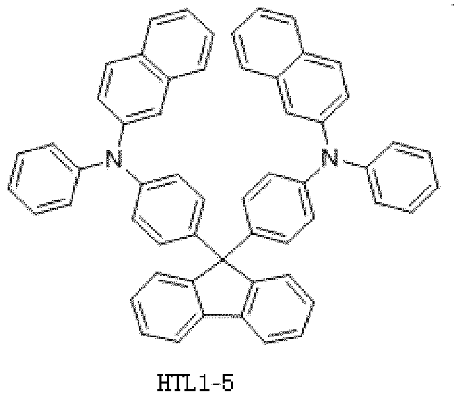
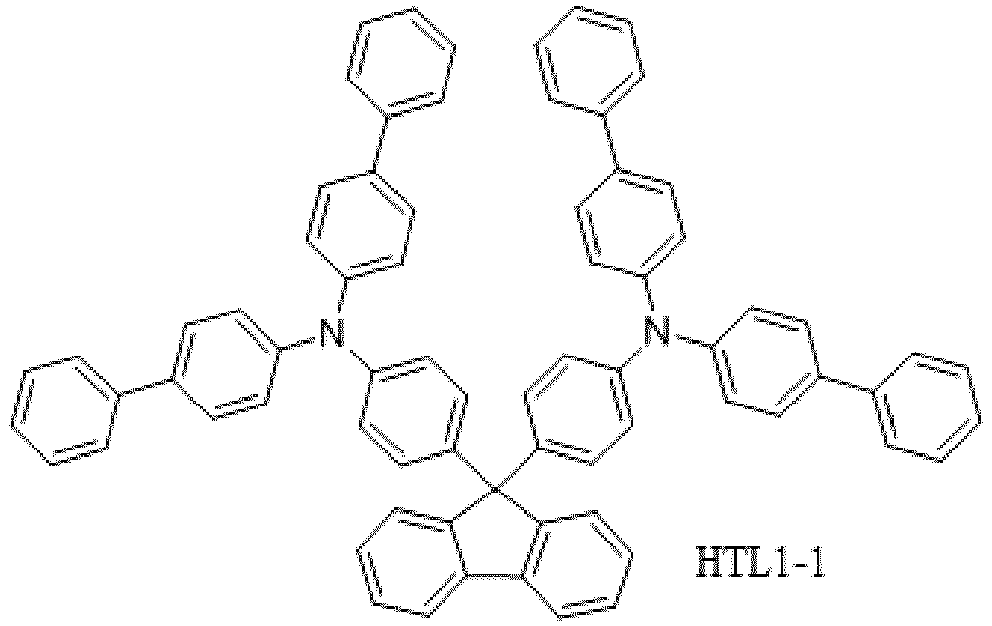
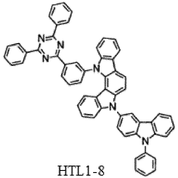
- the first hole transport material has a structure selected from the following structural formulas (HTL1-1) to (HTL21-10):
- the second hole transport material has an indenofluorene structure defined by the following structural formula (3), structural formula (4), structural formula (5) or structural formula (6): wherein, the groups of A and B are individually selected from phenyl group, naphthyl group or phenyl-amino group; the groups of R 9 , R 10 , R 11 and R 12 are identical or different, and are individually selected from C 6 -C 30 aryl group; the group of R 13 is selected from C 1 -C 6 alkyl group or hydroxyl group, preferably, the group R 13 is methyl group, ethyl group, propyl group, isopropyl group, butyl group, isobutyl group, n-amyl group or n-hexyl group.
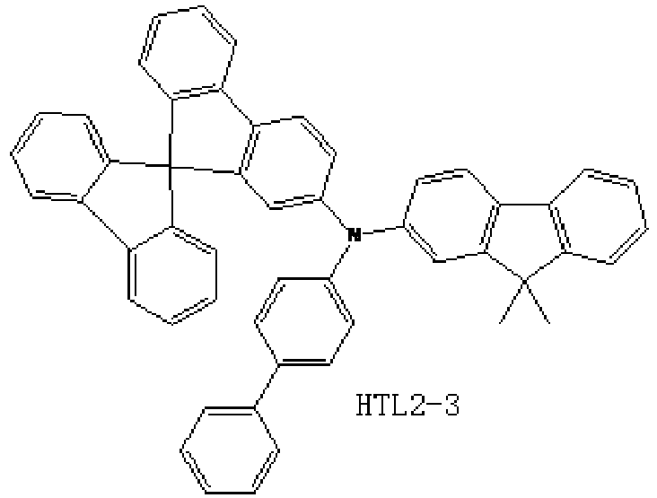
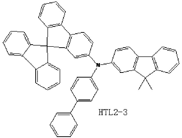
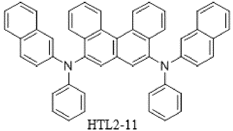
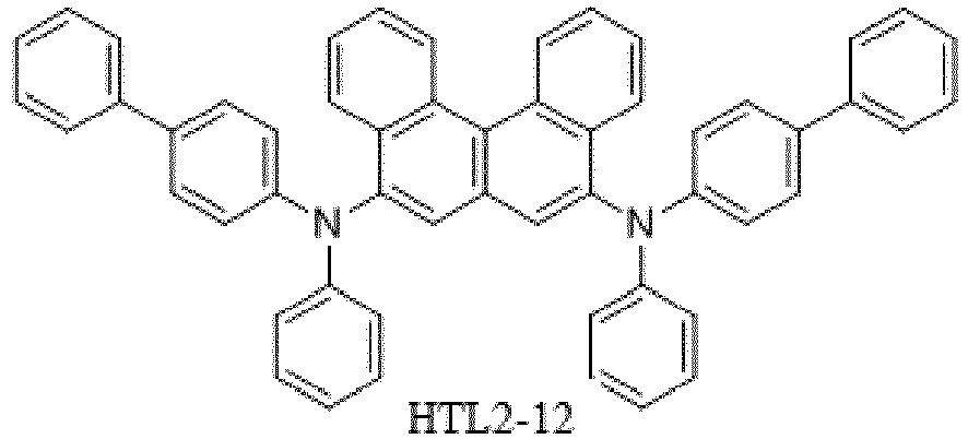
- the second hole transport material has a structure selected from the following structural formulas (HTL2-1) to (HTL2-18):
- the inventors of the present invention carry out creative research and daringly utilize a combination of a material having a high triplet-state energy level and a material having a high charge transfer rate to make the optical compensation layer of the present invention, and set the HOMO energy level difference between the two materials to be ⁇ 0.2eV, so that the optical compensation layer can be made to have different thicknesses according to requirements, and neither the light-emitting efficiency nor the drive voltage of the device is adversely affected. If the HOMO energy level difference between the two materials is too large, the first hole transport material cannot have an effect of blocking the green-light excitons.
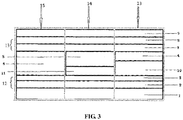
- FIG. 3 it is a structural schematic diagram of an organic electroluminescence device having RGB pixel areas in accordance with the present invention.
- This organic electroluminescence device having RGB pixel areas comprises a substrate (not shown in the drawing), with a first electrode layer 1 (anode layer), a plurality of organic layers, a second electrode layer 8 (cathode layer) and an optical coupling layer 9 formed in sequence on the substrate, wherein, the organic layers include a first organic functional layer 12, a light emitting layer and a second organic functional layer 13 arranged upon the first electrode layer 1, the light emitting layer comprises a red light emitting layer 4 with a thickness of H R , a green light emitting layer 5 with a thickness of H G and a blue light emitting layer 6 with a thickness of H B , where H B > H G > H R , and optical compensation layers are respectively arranged between the red light emitting layer 4 and the first organic functional layer 12 as well as between the green light emitting layer 5 and the first organic functional layer 12, the optical compensation layers are made of a first hole transport material and a second hole transport material, the first hole transport material has a triplet-state energy level ⁇ 2.48
- the optical compensation layers include a red light optical compensation layer 10 arranged between the red light emitting layer 4 and the first organic functional layer 12, and a green light optical compensation layer 11 arranged between the green light emitting layer 5 and the first organic functional layer 12.
- the first hole transport material and second hole transport material contained in the red light optical compensation layer 10 has a mass ratio of 1:99 to 99:1, preferably 10:90 to 30:70.
- the first hole transport material and second hole transport material contained in the green light optical compensation layer 11 has a mass ratio of 5:95 to 50:50, preferably 10:90 to 30:70.
- the first hole transport material has a structure defined by the following structural formula (1) or structural formula (2): in the structural formula (1), the groups A and B are individually selected from phenyl group, naphthyl group or phenyl-amino group; the groups of R 1 , R 2 , R 3 , R 4 , R5, R 6 , R 7 , R 8 , R 15 , R 16 , R 17 and R 18 are identical or different, and are individually selected from hydrogen element, halogen element, CN, NO 2 , amino group, C 6 -C 30 fused cyclic aryl group, C 6 -C 30 fused heterocyclic aryl group, C 6 -C 20 alkyl group or C 6 -C 30 alcohol group; the groups of R 9 , R 10 , R 11 and R 12 are identical or different, and are individually selected from C 6 -C 30 aryl group; in the structural formula (2), the groups of A1 and A2 are individually selected from C 6 -C 30 aryl group or C 6
- the first hole transport material has a structure selected from the following structural formulas (HTL21-1) to (HTL21-10):
- the second hole transport material has an indenofluorene structure defined by the following structural formula (3), structural formula (4), structural formula (5) or structural formula (6): wherein, the groups of A and B are individually selected from phenyl group, naphthyl group or phenyl-amino group; the groups of R 9 , R 10 , R 11 and R 12 are identical or different, and are individually selected from C 6 -C 30 aryl group; the group of R 13 is selected from C 1 -C 6 alkyl group or hydroxyl group, preferably, the group R 13 is methyl group, ethyl group, propyl group, isopropyl group, butyl group, isobutyl group, n-amyl group or n-hexyl group.
- the second hole transport material has a structure selected from the following structural formulas (HTL2-1) to (HTL2-18):
- the substrate is selected from a glass substrate or a flexible substrate.
- the first electrode layer 1 can adopt an inorganic material or an organic conducting polymer.
- the inorganic material is usually a metal oxide, such as indium tin oxide, zinc oxide, indium zinc oxide, or a metal with high work function, such as gold, copper, silver, preferably, it is indium tin oxide (ITO).
- the organic conducting polymer is preferably selected from Polythiophene / Polyethylene based sodium benzene sulfonate (hereinafter abbreviated as PEDOT:PSS) and Polyaniline (hereinafter abbreviated as PANI).
- the second electrode layer 8 (cathode layer) usually adopts metal, metal compound or alloy with low work function, such as lithium, magnesium, calcium, strontium, aluminum, indium.
- the electron transport layer 7 is preferably doped with an active metal such as Li, K, Cs which is preferably prepared by evaporation coating of an alkali metal compound.
- the hole injection layer 2 has a matrix material that is preferably HAT, 4,4-(N-3-methyl-phenyl-N-phenyl-amino)-triphenylamine (m-MTDATA), 4,4TDAT, or tri-(N-2-naphthyl-N-phenyl-amino)-triphenylamine (2-TNATA).
- the hole transport layer 3 has a matrix material that may adopt a low molecular material of the arylamine type or the branched polymer species, preferably N,N-di-(1-naphthyl)-N.N-diphenyl-1,1'-biphenyl-4,4'-diamine (NPB).
- the electron transport layer 7 has a material selected from Alq 3 , Bphen, BAlq or selected from the following materials:
- the blue light emitting layer 6 usually adopts a host material selected from ADN and its derivatives, together with a dye having a molecular structure selected from the following formula (BD-1) or formula (BD-2):
- the red light emitting layer 4 usually adopts the following material: Ir(piq) 3 , Ir(piq) 2 (acac), Btp 2 Ir(acac), Ir(MDQ) 2 (acac), Ir(DBQ) 2 (acac), Ir(fbi) 2 (acac), Ir(2-phq) 3 , Ir(2-phq) 2 (acac), Ir(bt) 2 (acac), PtOEP, etc.
- the green light emitting layer 5 usually adopts the following material: Ir(ppy) 3 , Ir(ppy) 2 (acac), etc.
- the organic electroluminescence device of Embodiments 1-14 has the following structures, and the differences thereof are different materials used by the red light optical compensation layer 10 and the green light optical compensation layer 11.
- Blue light emitting area 15 (within the leftmost dotted line block in FIG. 3 ): ITO/HAT(10nm)/MTDATA(100nm)/NPB(20nm)/ADN(30nm):BD-1/ETL-1(35nm)/Mg:Ag (20nm)/MTDATA(50nm)
- Green light emitting area 14 (within the middle dotted line block in FIG. 3 ): ITO/HAT(10nm)/MTDATA(100nm)/NPB(20nm)/HTL1:HTL2(60nm)/CBP(30nm):Ir(ppy)3/ ETL-1 (35nm)/Mg:Ag(20nm)/MTDATA(50nm)
- Red light emitting area 13 (within the rightmost dotted line block in FIG. 3 ): ITO/HAT(10nm)/MTDATA(100nm)/NPB(20nm)/HTL1:HTL2(110nm)/CBP(30nm): Ir(mdq)2(acac)/ETL-1(35nm)/Mg:Ag(20nm)/MTDATA(50nm)
- the first hole transport material HTL1 has a structure as shown by formula HTL1-1
- the second hole transport material HTL2 has a structure as shown by formula HTL2-1
- the first hole transport material HTL21-1 and second hole transport material HTL2-1 have a mass ratio of 50:50
- the first hole transport material HTL21-1 and second hole transport material HTL2-1 have a mass ratio of 50:50.
- the first hole transport material HTL1 has a structure as shown by formula HTL1-2
- the second hole transport material HTL2 has a structure as shown by formula HTL2-2
- the first hole transport material HTL1-2 and second hole transport material HTL2-2 have a mass ratio of 1:99
- the first hole transport material HTL1-2 and second hole transport material HTL2-2 have a mass ratio of 50:50.
- the first hole transport material HTL1 has a structure as shown by formula HTL1-3
- the second hole transport material HTL2 has a structure as shown by formula HTL2-3
- the first hole transport material HTL1-3 and second hole transport material HTL2-3 have a mass ratio of 99:1
- the first hole transport material HTL2-3 and second hole transport material HTL2-3 have a mass ratio of 95:5.
- the first hole transport material HTL1 has a structure as shown by formula HTL1-4
- the second hole transport material HTL2 has a structure as shown by formula HTL2-18
- the first hole transport material HTL1-4 and second hole transport material HTL2-18 have a mass ratio of 90:10
- the first hole transport material HTL1-4 and second hole transport material HTL2-18 have a mass ratio of 5:95.
- the first hole transport material HTL1 has a structure as shown by formula HTL1-5
- the second hole transport material HTL2 has a structure as shown by formula HTL2-16
- the first hole transport material HTL1-5 and second hole transport material HTL2-16 have a mass ratio of 70:30
- the first hole transport material HTL1-5 and second hole transport material HTL2-16 have a mass ratio of 15:85.
- the first hole transport material HTL1 has a structure as shown by formula HTL1-6
- the second hole transport material HTL2 has a structure as shown by formula HTL2-15
- the first hole transport material HTL1-6 and second hole transport material HTL2-15 have a mass ratio of 40:60
- the first hole transport material HTL1-6 and second hole transport material HTL2-15 have a mass ratio of 40:60.
- the first hole transport material HTL1 has a structure as shown by formula HTL1-7
- the second hole transport material HTL2 has a structure as shown by formula HTL2-14
- the first hole transport material HTL1-7 and second hole transport material HTL2-14 have a mass ratio of 50:50
- the first hole transport material HTL1-7 and second hole transport material HTL2-14 have a mass ratio of 30:70.
- the first hole transport material HTL1 has a structure as shown by formula HTL1-8
- the second hole transport material HTL2 has a structure as shown by formula HTL2-13
- the first hole transport material HTL1-8 and second hole transport material HTL2-13 have a mass ratio of 35:65
- the first hole transport material HTL1-8 and second hole transport material HTL2-13 have a mass ratio of 25:75.
- the first hole transport material HTL1 has a structure as shown by formula HTL1-9
- the second hole transport material HTL2 has a structure as shown by formula HTL2-12
- the first hole transport material HTL1-9 and second hole transport material HTL2-12 have a mass ratio of 90:10
- the first hole transport material HTL1-9 and second hole transport material HTL2-12 have a mass ratio of 45:55.
- the first hole transport material HTL1 has a structure as shown by formula HTL1-10
- the second hole transport material HTL2 has a structure as shown by formula HTL2-11 or HTL2-6
- the first hole transport material HTL1-10 and second hole transport material HTL2-11 have a mass ratio of 45:55
- the first hole transport material HTL1-10 and second hole transport material HTL2-6 have a mass ratio of 10:90.
- the first hole transport material HTL1 has a structure as shown by formula HTL1-1
- the second hole transport material HTL2 has a structure as shown by formula HTL2-10
- the first hole transport material HTL21-1 and second hole transport material HTL2-10 have a mass ratio of 95:5
- the first hole transport material HTL21-1 and second hole transport material HTL2-10 have a mass ratio of 5:95.
- the first hole transport material HTL1 has a structure as shown by formula HTL1-3
- the second hole transport material HTL2 has a structure as shown by formula HTL2-9 or HTL2-17
- the first hole transport material HTL1-3 and second hole transport material HTL2-17 have a mass ratio of 55:45
- the first hole transport material HTL1-3 and second hole transport material HTL2-9 have a mass ratio of 20:80.
- the first hole transport material HTL1 has a structure as shown by formula HTL1-5
- the second hole transport material HTL2 has a structure as shown by formula HTL2-8 or HTL2-4
- the first hole transport material HTL1-5 and second hole transport material HTL2-8 have a mass ratio of 55:45
- the first hole transport material HTL1-5 and second hole transport material HTL2-4 have a mass ratio of 20:80.
- the first hole transport material HTL1 has a structure as shown by formula HTL1-8
- the second hole transport material HTL2 has a structure as shown by formula HTL2-5 or HTL2-7
- the first hole transport material HTL1-8 and second hole transport material HTL2-7 have a mass ratio of 30:70
- the first hole transport material HTL1-8 and second hole transport material HTL2-5 have a mass ratio of 40:60.
- Blue light emitting area 15 (within the leftmost dotted line block in FIG. 3 ): ITO/HAT(10nm)/MTDATA(100nm)/NPB(20nm)/ADN(30nm):BD-1/ETL-1(35nm)/Mg:Ag (20nm)/MTDATA(50nm)
- Green light emitting area 14 (within the middle dotted line block in FIG. 3 ): ITO/HAT(10nm)/MTDATA(160nm)/NPB(20nm)/CBP(30nm):Ir(ppy) 3 /ETL-1(35nm)/ Mg:Ag(20nm)/MTDATA(50nm)
- Red light emitting area 13 (within the rightmost dotted line block in FIG. 3 ): ITO/HAT(10nm)/MTDATA(210nm)/NPB(20nm)/CBP(30nm):Ir(mdq) 2 (acac)/ETL-1(35nm)/ Mg:Ag(20nm)/MTDATA(50nm)
- the optical compensation layers is made of a combination of a hole transport material having a high energy level and a material having a high charge transfer rate, the light emitting efficiencies of the red light emitting layer and the green light emitting layer are significantly increased.
Landscapes
- Chemical & Material Sciences (AREA)
- Organic Chemistry (AREA)
- Physics & Mathematics (AREA)
- Optics & Photonics (AREA)
- Spectroscopy & Molecular Physics (AREA)
- Engineering & Computer Science (AREA)
- Materials Engineering (AREA)
- Electromagnetism (AREA)
- Electroluminescent Light Sources (AREA)
- Devices For Indicating Variable Information By Combining Individual Elements (AREA)
Abstract
Description
- The present invention pertains to the technical field of organic electroluminescence devices, and in particular relates to an organic electroluminescence device having optical compensation layers.
- The light-emitting layer of an organic electroluminescence device OLED is mainly made of fluorescent material, or phosphorescent material, or mixed fluorescent and phosphorescent material. The LED display unit consists of three kinds of red, green, blue pixels, and when a top-emitting OLED device structure is used, because the three kinds of pixels have different light-emitting wavelengths, the thicknesses of the light-emitting layers would have certain differences. Usually, an optical compensation layer is utilized to modify the thickness of a light-emitting layer, the thickness of the optical compensation layer can be over 100nm, so the optical compensation layer needs to have very good electrical charge transfer rate, in order to ensure that the device has the characteristics of low voltage and high efficiency.
- The material used to make the existing optical compensation layer has a high triplet-state energy level, but often has low charge transfer rate and thus cannot be made to be thick enough, therefore, as an optical compensation layer, it has a high drive voltage. In another aspect, material with a high charge transfer rate often has a low triplet-state energy level, which adversely affects the efficiency of green-light devices. Currently, the optical compensation layer is arranged between HIL and HTL, and is made of material with a high hole transfer rate (1.5-2 times of the transfer rate of NPB), although such arrangement alleviates the thickness increase of the organic layer to a certain extent and does not adversely affect the drive voltage of the organic light-emitting device, it does not take the special electric characteristic requirements of different light-emitting material into consideration, and cannot effectively increase the efficiency of the organic light-emitting device and reduce the power consumption of the display device.
- The patent literature
CN201210395191.7 FIG. 1 , it sequentially comprises asubstrate 110, afirst electrode 120, ahole injection layer 130, ahole transport layer 140, abuffer layer 150, a light-emitting layer 160, anelectron transport layer 170, anelectron injection layer 180 and asecond electrode 190. Thehole transport layer 140 consists of sequentially deposited layers of a firstcharge generation layer 141, a first mixedlayer 142, a secondcharge generation layer 143 and a second mixedlayer 144. The firstcharge generation layer 141 can be made of a mixture that contains a first compound and a second compound and is doped with a first charge generation material; the first mixedlayer 142 can be made of a mixture that contains the first compound and the second compound; the secondcharge generation layer 143 can be made of a mixture that contains a third compound and a fourth compound and is doped with a second charge generation material; the second mixedlayer 144 can be made of a mixture that contains the third compound and the fourth compound, in this aspect, the third compound and the fourth compound has a weigh ratio of 6:4 to 8:2. In this patent, the charge generation layer cannot provide an effective function for blocking excitons, so the buffer layer is required. - The patent literature
CN200510077967.0 FIG. 2 , a second hole transport layer 18-2 is arranged upon a first hole transport layer 18-1 in a green-light pixel area 200; the second hole transport layer 18-2 and a third hole transport layer 18-3 are arranged upon the first hole transport layer 18-1 in a red-light pixel area 300. The first hole transport layer 18-1, the second hole transport layer 18-2 and the third hole transport layer 18-3 can be made of different materials, but these hole transport layers are made of the same material. Although this patent discloses utilization of hole transport layers with a mixed structure to increase light-emitting efficiency and such arrangement alleviates the thickness of the light-emitting layer to a certain extent, the HTL material suitable to make the green-light optical compensation layer is still required to have a high triplet-state energy level T1 with its HOMO energy level ≤ -5.5eV, and this kind of material often has a low charge transfer rate and thus cannot be made to be thick enough, therefore, this device has a high drive voltage. - Accordingly, one objective of the present invention is to solve the technical problem that the red-light and green-light optical compensation layers in prior art are made of materials with a low charge transfer rate or a poor exciton blocking effect, by providing an organic electroluminescence device that has an optical compensation layer made of two hole transport materials with different energy gaps, which can significantly reduce power consumption of the light-emitting device, so as to increase light-emitting efficiency.
- The present invention also provides a preparation method of the above-mentioned organic electroluminescence device.
- In order to solve the above-mentioned technical problem, the present invention adopts the following technical scheme:
- An organic electroluminescence device having RGB pixel areas comprises a substrate, with a first electrode layer, a plurality of organic layers and a second electrode layer formed in sequence on the substrate, wherein, the organic layers include a first organic functional layer, a light emitting layer and a second organic functional layer arranged upon the first electrode layer, the light emitting layer comprises a red light emitting layer, a green light emitting layer and a blue light emitting layer, wherein, optical compensation layers are respectively arranged between the red light emitting layer and the first organic functional layer as well as between the green light emitting layer and the first organic functional layer, the optical compensation layers are made of a first hole transport material and a second hole transport material, the first hole transport material has a triplet-state energy level ≥ 2.48eV and a HOMO energy level ≤ -5.5eV, the second hole transport material has a HOMO energy level > -5.5eV, and the difference between the HOMO energy level of the first hole transport material and the HOMO energy level of the second hole transport material is ≤ 0.2eV.
- The optical compensation layers include a red light optical compensation layer arranged between the red light emitting layer and the first organic functional layer, and a green light optical compensation layer arranged between the green light emitting layer and the first organic functional layer.
- The first hole transport material and second hole transport material contained in the red light optical compensation layer has a mass ratio of 1:99 to 99:1.
- The first hole transport material and second hole transport material contained in the green light optical compensation layer has a mass ratio of 5:95 to 50:50, preferably 10:90 to 30:70.
- The first hole transport material has a structure defined by the following structural formula (1) or structural formula (2):


the groups of R1, R2, R3, R4, R5, R6, R7, R8, R15, R16, R17 and R18 are identical or different, and are individually selected from hydrogen element, halogen element, CN, NO2, amino group, C6-C30 fused cyclic aryl group, C6-C30 fused heterocyclic aryl group, C6-C20 alkyl group or C6-C30 alcohol group;
the groups of R9, R10, R11 and R12 are identical or different, and are individually selected from C6-C30 aryl group;
in the structural formula (2), the groups of A1 and A2 are individually selected from C6-C30 aryl group or C6-C30 heterocyclic aryl group, the group R1' is selected from hydrogen, alkyl group, alkoxyl group or basic group;
and the structural formula (2) also meets the following condition: at least one of the groups of A1 and A2 has a condensed ring structure. - The first hole transport material has a structure selected from the following structural formulas (HTL1-1) to (HTL21-10):


- The second hole transport material has an indenofluorene structure defined by the following structural formula (3), structural formula (4), structural formula (5) or structural formula (6):


the groups of R9, R10, R11 and R12 are identical or different, and are individually selected from C6-C30 aryl group;
the group of R13 is selected from C1-C6 alkyl group or hydroxyl group, preferably, the group R13 is methyl group, ethyl group, propyl group, isopropyl group, butyl group, isobutyl group, n-amyl group or n-hexyl group. - The second hole transport material has a structure selected from the following structural formulas (HTL2-1) to (HTL2-18):




- As compared to prior art, the above-mentioned technical scheme of the present invention has the following advantages:
- In the organic electroluminescence display device of the present invention, optical compensation layers are arranged between the light-emitting layer and the hole transport layer, and in the evaporation coating process of the optical compensation layers with such structure, the red-light optical compensation layer and the red light emitting layer can be prepared by using the same group of mask, the green-light optical compensation layer and the green light emitting layer can be prepared by using the same group of mask, which can avoid repeated aligning operations of the masks and thus increase the process precision to a certain extent. This is because every aligning operation of the masks always has certain error, therefore, with less times of aligning operations, the error is less and the overall yield is higher.
- Furthermore, the inventors of the present invention carry out creative research and daringly utilize a combination of a material having a high triplet-state energy level and a material having a high charge transfer rate to make the optical compensation layer of the present invention, and set the HOMO energy level difference between the two materials to be ≤ 0.2eV, so that the optical compensation layer can be made to have different thicknesses according to requirements, and neither the light-emitting efficiency nor the drive voltage of the device is adversely affected. If the HOMO energy level difference between the two materials is too large, the first hole transport material cannot have an effect of blocking the green-light excitons.
- In order to make the content of the present invention more easy to be understood clearly, hereinafter, detailed description of the present invention is further provided according to specific embodiments of the present invention with reference to the appended drawings, wherein,
-
FIG. 1 is a structural schematic diagram of a light-emitting device in prior art; -
FIG. 2 is a structural schematic diagram of another light-emitting device in prior art; -
FIG. 3 is a structural schematic diagram of a light-emitting device of the present invention. - Wherein, 1-first electrode layer, 2-hole injection layer, 3-hole transport layer, 4-red light emitting layer, 5-green light emitting layer, 6-blue light emitting layer, 7-electron transport layer, 8-second electrode layer, 9-optical coupling layer, 10-red light optical compensation layer, 11-green light optical compensation layer, 12-first organic functional layer, 13-second organic functional layer.
- In order to make the objective, technical scheme and advantages of the present invention more clear, hereinafter, detailed description of implementation ways of the present invention is given below, with reference to the appended drawings.
- The present invention may be implemented in many different ways, and should not be interpreted to be limited to the embodiments described herein. On the contrary, by providing these embodiments, the present disclosure is made complete and thorough, and the inventive concept of the present invention is sufficiently conveyed to those skilled in the art, wherein the present invention is defined by the claims. In the appended drawings, for the sake of clarity, dimensions and relative sizes of layers and areas might be exaggerated. It should be understood that, when one element such as a layer, an area or a substrate plate is described as "formed on" or "configured on" another element, this one element may be configured directly upon that another element, or there may exist intermediate element(s). On the contrary, when one element is described as "directly formed upon" or "directly configured upon" another element, there exist no intermediate element.
- As shown in
FIG. 3 , it is a structural schematic diagram of an organic electroluminescence device having RGB pixel areas in accordance with the present invention. - This organic electroluminescence device having RGB pixel areas comprises a substrate (not shown in the drawing), with a first electrode layer 1 (anode layer), a plurality of organic layers, a second electrode layer 8 (cathode layer) and an optical coupling layer 9 formed in sequence on the substrate, wherein, the organic layers include a first organic
functional layer 12, a light emitting layer and a second organicfunctional layer 13 arranged upon thefirst electrode layer 1, the light emitting layer comprises a red light emitting layer 4 with a thickness of HR, a green light emitting layer 5 with a thickness of HG and a blue light emitting layer 6 with a thickness of HB, where HB > HG > HR, and optical compensation layers are respectively arranged between the red light emitting layer 4 and the first organicfunctional layer 12 as well as between the green light emitting layer 5 and the first organicfunctional layer 12, the optical compensation layers are made of a first hole transport material and a second hole transport material, the first hole transport material has a triplet-state energy level ≥ 2.48eV and a HOMO energy level ≤ -5.5eV, the second hole transport material has a HOMO energy level > -5.5eV, and the difference between the HOMO energy level of the first hole transport material and the HOMO energy level of the second hole transport material is ≤ 0.2eV - The optical compensation layers include a red light
optical compensation layer 10 arranged between the red light emitting layer 4 and the first organicfunctional layer 12, and a green lightoptical compensation layer 11 arranged between the green light emitting layer 5 and the first organicfunctional layer 12. The first hole transport material and second hole transport material contained in the red lightoptical compensation layer 10 has a mass ratio of 1:99 to 99:1, preferably 10:90 to 30:70. The first hole transport material and second hole transport material contained in the green lightoptical compensation layer 11 has a mass ratio of 5:95 to 50:50, preferably 10:90 to 30:70. - The first hole transport material has a structure defined by the following structural formula (1) or structural formula (2):


the groups of R1, R2, R3, R4, R5, R6, R7, R8, R15, R16, R17 and R18 are identical or different, and are individually selected from hydrogen element, halogen element, CN, NO2, amino group, C6-C30 fused cyclic aryl group, C6-C30 fused heterocyclic aryl group, C6-C20 alkyl group or C6-C30 alcohol group;
the groups of R9, R10, R11 and R12 are identical or different, and are individually selected from C6-C30 aryl group;
in the structural formula (2), the groups of A1 and A2 are individually selected from C6-C30 aryl group or C6-C30 heterocyclic aryl group, the group R1' is selected from hydrogen, alkyl group, alkoxyl group or basic group;
and the structural formula (2) also meets the following condition: at least one of the groups of A1 and A2 has a condensed ring structure. - The first hole transport material has a structure selected from the following structural formulas (HTL21-1) to (HTL21-10):




- The second hole transport material has an indenofluorene structure defined by the following structural formula (3), structural formula (4), structural formula (5) or structural formula (6):


the groups of R9, R10, R11 and R12 are identical or different, and are individually selected from C6-C30 aryl group;
the group of R13 is selected from C1-C6 alkyl group or hydroxyl group, preferably, the group R13 is methyl group, ethyl group, propyl group, isopropyl group, butyl group, isobutyl group, n-amyl group or n-hexyl group. - The second hole transport material has a structure selected from the following structural formulas (HTL2-1) to (HTL2-18):




- The substrate is selected from a glass substrate or a flexible substrate.
- The first electrode layer 1 (anode layer) can adopt an inorganic material or an organic conducting polymer. The inorganic material is usually a metal oxide, such as indium tin oxide, zinc oxide, indium zinc oxide, or a metal with high work function, such as gold, copper, silver, preferably, it is indium tin oxide (ITO). The organic conducting polymer is preferably selected from Polythiophene / Polyethylene based sodium benzene sulfonate (hereinafter abbreviated as PEDOT:PSS) and Polyaniline (hereinafter abbreviated as PANI).
- The second electrode layer 8 (cathode layer) usually adopts metal, metal compound or alloy with low work function, such as lithium, magnesium, calcium, strontium, aluminum, indium. In the present invention, the electron transport layer 7 is preferably doped with an active metal such as Li, K, Cs which is preferably prepared by evaporation coating of an alkali metal compound.
- The hole injection layer 2 (HIL) has a matrix material that is preferably HAT, 4,4-(N-3-methyl-phenyl-N-phenyl-amino)-triphenylamine (m-MTDATA), 4,4TDAT, or tri-(N-2-naphthyl-N-phenyl-amino)-triphenylamine (2-TNATA).
- The hole transport layer 3 (HTL) has a matrix material that may adopt a low molecular material of the arylamine type or the branched polymer species, preferably N,N-di-(1-naphthyl)-N.N-diphenyl-1,1'-biphenyl-4,4'-diamine (NPB).
- The electron transport layer 7 has a material selected from Alq3, Bphen, BAlq or selected from the following materials:


- The blue light emitting layer 6 usually adopts a host material selected from ADN and its derivatives, together with a dye having a molecular structure selected from the following formula (BD-1) or formula (BD-2):


- The red light emitting layer 4 usually adopts the following material: Ir(piq)3, Ir(piq)2(acac), Btp2Ir(acac), Ir(MDQ)2(acac), Ir(DBQ)2(acac), Ir(fbi)2(acac), Ir(2-phq)3, Ir(2-phq)2(acac), Ir(bt)2(acac), PtOEP, etc.
- The green light emitting layer 5 usually adopts the following material: Ir(ppy)3, Ir(ppy)2(acac), etc.
- The structural formulas of the main chemical substances in the present invention are explained as follows:
Abbreviation Structural Formula NPB 
HAT 
MTDATA 
Ir(ppy)3 
Ir(MDQ)2(acac) 
ADN 
BPhen 
- Some embodiments are given below, for specifically explaining the technical scheme of the present invention with reference to the appended drawings. It should be noted that, the following embodiments are only intended to help understanding the present invention, not to limit the present invention.
- The organic electroluminescence device of Embodiments 1-14 has the following structures, and the differences thereof are different materials used by the red light
optical compensation layer 10 and the green lightoptical compensation layer 11. - Blue light emitting area 15 (within the leftmost dotted line block in
FIG. 3 ): ITO/HAT(10nm)/MTDATA(100nm)/NPB(20nm)/ADN(30nm):BD-1/ETL-1(35nm)/Mg:Ag (20nm)/MTDATA(50nm) - Green light emitting area 14 (within the middle dotted line block in
FIG. 3 ): ITO/HAT(10nm)/MTDATA(100nm)/NPB(20nm)/HTL1:HTL2(60nm)/CBP(30nm):Ir(ppy)3/ ETL-1 (35nm)/Mg:Ag(20nm)/MTDATA(50nm) - Red light emitting area 13 (within the rightmost dotted line block in
FIG. 3 ): ITO/HAT(10nm)/MTDATA(100nm)/NPB(20nm)/HTL1:HTL2(110nm)/CBP(30nm): Ir(mdq)2(acac)/ETL-1(35nm)/Mg:Ag(20nm)/MTDATA(50nm) - Wherein, the first hole transport material HTL1 has a structure as shown by formula HTL1-1, and the second hole transport material HTL2 has a structure as shown by formula HTL2-1; In the red light
optical compensation layer 10, the first hole transport material HTL21-1 and second hole transport material HTL2-1 have a mass ratio of 50:50;
In the green lightoptical compensation layer 11, the first hole transport material HTL21-1 and second hole transport material HTL2-1 have a mass ratio of 50:50. - Wherein, the first hole transport material HTL1 has a structure as shown by formula HTL1-2, and the second hole transport material HTL2 has a structure as shown by formula HTL2-2; In the red light
optical compensation layer 10, the first hole transport material HTL1-2 and second hole transport material HTL2-2 have a mass ratio of 1:99;
In the green lightoptical compensation layer 11, the first hole transport material HTL1-2 and second hole transport material HTL2-2 have a mass ratio of 50:50. - Wherein, the first hole transport material HTL1 has a structure as shown by formula HTL1-3, and the second hole transport material HTL2 has a structure as shown by formula HTL2-3; In the red light
optical compensation layer 10, the first hole transport material HTL1-3 and second hole transport material HTL2-3 have a mass ratio of 99:1;
In the green lightoptical compensation layer 11, the first hole transport material HTL2-3 and second hole transport material HTL2-3 have a mass ratio of 95:5. - Wherein, the first hole transport material HTL1 has a structure as shown by formula HTL1-4, and the second hole transport material HTL2 has a structure as shown by formula HTL2-18; In the red light
optical compensation layer 10, the first hole transport material HTL1-4 and second hole transport material HTL2-18 have a mass ratio of 90:10;
In the green lightoptical compensation layer 11, the first hole transport material HTL1-4 and second hole transport material HTL2-18 have a mass ratio of 5:95. - Wherein, the first hole transport material HTL1 has a structure as shown by formula HTL1-5, and the second hole transport material HTL2 has a structure as shown by formula HTL2-16; In the red light
optical compensation layer 10, the first hole transport material HTL1-5 and second hole transport material HTL2-16 have a mass ratio of 70:30;
In the green lightoptical compensation layer 11, the first hole transport material HTL1-5 and second hole transport material HTL2-16 have a mass ratio of 15:85. - Wherein, the first hole transport material HTL1 has a structure as shown by formula HTL1-6, and the second hole transport material HTL2 has a structure as shown by formula HTL2-15; In the red light
optical compensation layer 10, the first hole transport material HTL1-6 and second hole transport material HTL2-15 have a mass ratio of 40:60;
In the green lightoptical compensation layer 11, the first hole transport material HTL1-6 and second hole transport material HTL2-15 have a mass ratio of 40:60. - Wherein, the first hole transport material HTL1 has a structure as shown by formula HTL1-7, and the second hole transport material HTL2 has a structure as shown by formula HTL2-14; In the red light
optical compensation layer 10, the first hole transport material HTL1-7 and second hole transport material HTL2-14 have a mass ratio of 50:50;
In the green lightoptical compensation layer 11, the first hole transport material HTL1-7 and second hole transport material HTL2-14 have a mass ratio of 30:70. - Wherein, the first hole transport material HTL1 has a structure as shown by formula HTL1-8, and the second hole transport material HTL2 has a structure as shown by formula HTL2-13; In the red light
optical compensation layer 10, the first hole transport material HTL1-8 and second hole transport material HTL2-13 have a mass ratio of 35:65;
In the green lightoptical compensation layer 11, the first hole transport material HTL1-8 and second hole transport material HTL2-13 have a mass ratio of 25:75. - Wherein, the first hole transport material HTL1 has a structure as shown by formula HTL1-9, and the second hole transport material HTL2 has a structure as shown by formula HTL2-12; In the red light
optical compensation layer 10, the first hole transport material HTL1-9 and second hole transport material HTL2-12 have a mass ratio of 90:10;
In the green lightoptical compensation layer 11, the first hole transport material HTL1-9 and second hole transport material HTL2-12 have a mass ratio of 45:55. - Wherein, the first hole transport material HTL1 has a structure as shown by formula HTL1-10, and the second hole transport material HTL2 has a structure as shown by formula HTL2-11 or HTL2-6;
In the red lightoptical compensation layer 10, the first hole transport material HTL1-10 and second hole transport material HTL2-11 have a mass ratio of 45:55;
In the green lightoptical compensation layer 11, the first hole transport material HTL1-10 and second hole transport material HTL2-6 have a mass ratio of 10:90. - Wherein, the first hole transport material HTL1 has a structure as shown by formula HTL1-1, and the second hole transport material HTL2 has a structure as shown by formula HTL2-10; In the red light
optical compensation layer 10, the first hole transport material HTL21-1 and second hole transport material HTL2-10 have a mass ratio of 95:5;
In the green lightoptical compensation layer 11, the first hole transport material HTL21-1 and second hole transport material HTL2-10 have a mass ratio of 5:95. - Wherein, the first hole transport material HTL1 has a structure as shown by formula HTL1-3, and the second hole transport material HTL2 has a structure as shown by formula HTL2-9 or HTL2-17;
In the red lightoptical compensation layer 10, the first hole transport material HTL1-3 and second hole transport material HTL2-17 have a mass ratio of 55:45;
In the green lightoptical compensation layer 11, the first hole transport material HTL1-3 and second hole transport material HTL2-9 have a mass ratio of 20:80. - Wherein, the first hole transport material HTL1 has a structure as shown by formula HTL1-5, and the second hole transport material HTL2 has a structure as shown by formula HTL2-8 or HTL2-4;
In the red lightoptical compensation layer 10, the first hole transport material HTL1-5 and second hole transport material HTL2-8 have a mass ratio of 55:45;
In the green lightoptical compensation layer 11, the first hole transport material HTL1-5 and second hole transport material HTL2-4 have a mass ratio of 20:80. - Wherein, the first hole transport material HTL1 has a structure as shown by formula HTL1-8, and the second hole transport material HTL2 has a structure as shown by formula HTL2-5 or HTL2-7;
In the red lightoptical compensation layer 10, the first hole transport material HTL1-8 and second hole transport material HTL2-7 have a mass ratio of 30:70;
In the green lightoptical compensation layer 11, the first hole transport material HTL1-8 and second hole transport material HTL2-5 have a mass ratio of 40:60. - Blue light emitting area 15 (within the leftmost dotted line block in
FIG. 3 ): ITO/HAT(10nm)/MTDATA(100nm)/NPB(20nm)/ADN(30nm):BD-1/ETL-1(35nm)/Mg:Ag (20nm)/MTDATA(50nm) - Green light emitting area 14 (within the middle dotted line block in
FIG. 3 ): ITO/HAT(10nm)/MTDATA(160nm)/NPB(20nm)/CBP(30nm):Ir(ppy)3/ETL-1(35nm)/ Mg:Ag(20nm)/MTDATA(50nm) - Red light emitting area 13 (within the rightmost dotted line block in
FIG. 3 ): ITO/HAT(10nm)/MTDATA(210nm)/NPB(20nm)/CBP(30nm):Ir(mdq)2(acac)/ETL-1(35nm)/ Mg:Ag(20nm)/MTDATA(50nm) - The test results of the devices are listed below:
Blue light efficiency (cd/A) Green light efficiency (cd/A) Red light efficiency (cd/A) Embodiment 14.3 70.2 29.3 Embodiment 24.3 66.3 29.8 Embodiment 3 4.3 69.5 32.1 Embodiment 4 4.3 72.5 30.6 Embodiment 5 4.3 72.1 28.4 Embodiment 6 4.3 67.0 34.2 Embodiment 7 4.3 69.4 30.3 Embodiment 8 4.3 75.1 36.7 Embodiment 9 4.3 65.2 33.1 Embodiment 104.3 64.2 27.0 Embodiment 114.3 69.0 28.9 Embodiment 124.3 65.9 27.0 Embodiment 134.3 71.5 33.5 Embodiment 144.3 72.2 30.4 Comparison Example 4.3 63.3 26.9 - As indicated by the test results, because the optical compensation layers is made of a combination of a hole transport material having a high energy level and a material having a high charge transfer rate, the light emitting efficiencies of the red light emitting layer and the green light emitting layer are significantly increased.
- Apparently, the aforementioned embodiments are merely examples illustrated for clearly describing the present invention, rather than limiting the implementation ways thereof. For those skilled in the art, various changes and modifications in other different forms can be made on the basis of the aforementioned description. It is unnecessary and impossible to exhaustively list all the implementation ways herein. However, any obvious changes or modifications derived from the aforementioned description are intended to be embraced within the protection scope of the present invention.
Claims (10)
- An organic electroluminescence device having RGB pixel areas, comprising a substrate, with a first electrode layer (1), a plurality of organic layers and a second electrode layer (8) formed in sequence on the substrate, wherein, the organic layers include a first organic functional layer (12), a light emitting layer and a second organic functional layer (13) arranged upon the first electrode layer (1), the light emitting layer comprises a red light emitting layer (4), a green light emitting layer (5) and a blue light emitting layer (6),
characterized in that,
optical compensation layers are respectively arranged between the red light emitting layer (4) and the first organic functional layer (12) as well as between the green light emitting layer (5) and the first organic functional layer (12), the optical compensation layers are made of a first hole transport material and a second hole transport material, the first hole transport material has a triplet-state energy level ≥ 2.48eV and a HOMO energy level ≤ -5.5eV, the second hole transport material has a HOMO energy level > -5.5eV, and the difference between the HOMO energy level of the first hole transport material and the HOMO energy level of the second hole transport material is ≤ 0.2eV. - The organic electroluminescence device having RGB pixel areas of Claim 1, characterized in that, the optical compensation layers include a red light optical compensation layer (10) arranged between the red light emitting layer (4) and the first organic functional layer (12), and a green light optical compensation layer (11) arranged between the green light emitting layer (5) and the first organic functional layer (12).
- The organic electroluminescence device having RGB pixel areas of Claim 2, characterized in that, the first hole transport material and second hole transport material contained in the red light optical compensation layer (10) has a mass ratio of 1:99 to 99:1.
- The organic electroluminescence device having RGB pixel areas of Claim 2, characterized in that, the first hole transport material and second hole transport material contained in the green light optical compensation layer (11) has a mass ratio of 5:95 to 50:50.
- The organic electroluminescence device having RGB pixel areas of Claim 4, characterized in that, the first hole transport material and second hole transport material contained in the green light optical compensation layer (11) has a mass ratio of 10:90 to 30:70.
- The organic electroluminescence device having RGB pixel areas of any one of Claims 1-5, characterized in that, the first hole transport material has a structure defined by the following structural formula (1) or structural formula (2):


the groups of R1, R2, R3, R4, R5, R6, R7, R8, R15, R16, R17 and R18 are identical or different, and are individually selected from hydrogen element, halogen element, CN, NO2, amino group, C6-C30 fused cyclic aryl group, C6-C30 fused heterocyclic aryl group, C6-C20 alkyl group or C6-C30 alcohol group;
the groups of R9, R10, R11 and R12 are identical or different, and are individually selected from C6-C30 aryl group;
in the structural formula (2), the groups of A1 and A2 are individually selected from C6-C30 aryl group or C6-C30 heterocyclic aryl group, the group R1' is selected from hydrogen, alkyl group, alkoxyl group or basic group;
and the structural formula (2) also meets the following condition: at least one of the groups of A 1 and A2 has a condensed ring structure. - The organic electroluminescence device having RGB pixel areas of Claim 6, characterized in that, the first hole transport material has a structure selected from the following structural formulas (HTL1-1) to (HTL1-10) :




- The organic electroluminescence device having RGB pixel areas of any one of Claims 1-5, characterized in that, the second hole transport material has an indenofluorene structure defined by the following structural formula (3), structural formula (4), structural formula (5) or structural formula (6):


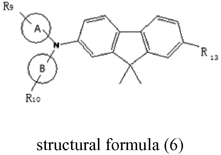
the groups of R9, R10, R11 and R12 are identical or different, and are individually selected from C6-C30 aryl group;
the group of R13 is selected from C1-C6 alkyl group or hydroxyl group. - The organic electroluminescence device having RGB pixel areas of Claim 8, characterized in that, the group R13 is methyl group, ethyl group, propyl group, isopropyl group, butyl group, isobutyl group, n-amyl group or n-hexyl group.
- The organic electroluminescence device having RGB pixel areas of Claim 8, characterized in that, the second hole transport material has a structure selected from the following structural formulas (HTL2-1) to (HTL2-18):




Applications Claiming Priority (2)
| Application Number | Priority Date | Filing Date | Title |
|---|---|---|---|
| CN201410853953.2A CN104538559B (en) | 2014-12-31 | 2014-12-31 | A kind of organic electroluminescence display device and method of manufacturing same with rgb pixel area |
| PCT/CN2015/099376 WO2016107537A1 (en) | 2014-12-31 | 2015-12-29 | Organic electroluminescence device having rgb pixel areas |
Publications (3)
| Publication Number | Publication Date |
|---|---|
| EP3242343A1 true EP3242343A1 (en) | 2017-11-08 |
| EP3242343A4 EP3242343A4 (en) | 2018-08-15 |
| EP3242343B1 EP3242343B1 (en) | 2019-10-16 |
Family
ID=52854056
Family Applications (1)
| Application Number | Title | Priority Date | Filing Date |
|---|---|---|---|
| EP15875213.9A Active EP3242343B1 (en) | 2014-12-31 | 2015-12-29 | Organic electroluminescence device having rgb pixel areas |
Country Status (7)
| Country | Link |
|---|---|
| US (1) | US10693107B2 (en) |
| EP (1) | EP3242343B1 (en) |
| JP (1) | JP6571780B2 (en) |
| KR (1) | KR101946406B1 (en) |
| CN (1) | CN104538559B (en) |
| TW (1) | TWI570985B (en) |
| WO (1) | WO2016107537A1 (en) |
Cited By (1)
| Publication number | Priority date | Publication date | Assignee | Title |
|---|---|---|---|---|
| US11233201B2 (en) | 2017-06-30 | 2022-01-25 | Kunshan Go-Visionox Opto-Electronics Co., Ltd. | Organic electroluminescent devices and preparation methods thereof |
Families Citing this family (22)
| Publication number | Priority date | Publication date | Assignee | Title |
|---|---|---|---|---|
| CN104538559B (en) | 2014-12-31 | 2017-10-10 | 北京维信诺科技有限公司 | A kind of organic electroluminescence display device and method of manufacturing same with rgb pixel area |
| KR102397823B1 (en) * | 2015-11-30 | 2022-05-12 | 엘지디스플레이 주식회사 | Organic light emitting display device |
| CN105503622A (en) * | 2015-12-14 | 2016-04-20 | 武汉尚赛光电科技有限公司 | Benzo[c]phenanthrene derivative with electron donor-acceptor structure and application thereof and electroluminescent device |
| CN106887446A (en) * | 2015-12-15 | 2017-06-23 | 昆山工研院新型平板显示技术中心有限公司 | Organic light emitting display and display device |
| JP6816102B2 (en) * | 2016-03-01 | 2021-01-20 | パイオニア株式会社 | Manufacturing method of light emitting device |
| CN105837498B (en) * | 2016-04-25 | 2019-03-22 | 中节能万润股份有限公司 | Organic compound containing dimethylanthracene structure and application thereof |
| CN107056809B (en) * | 2016-04-25 | 2019-05-14 | 中节能万润股份有限公司 | An organic compound containing dimethyl anthracene and its application in organic electroluminescent devices |
| CN112117318B (en) * | 2016-07-29 | 2024-11-01 | 京东方科技集团股份有限公司 | OLED array substrate and manufacturing method thereof, and OLED display panel |
| CN107785490B (en) * | 2016-08-26 | 2019-12-24 | 昆山工研院新型平板显示技术中心有限公司 | Organic electroluminescent device |
| CN106409877B (en) * | 2016-11-21 | 2019-06-14 | 上海天马有机发光显示技术有限公司 | An organic light-emitting display panel and an organic light-emitting display device |
| CN106531896B (en) * | 2016-12-13 | 2018-08-10 | 上海天马有机发光显示技术有限公司 | Organic light emitting display device, manufacturing method thereof, and organic light emitting display device |
| CN108203429A (en) * | 2016-12-20 | 2018-06-26 | 江苏三月光电科技有限公司 | Using the nitrogenous hexa-member heterocycle of dibenzo as the compound and organic electroluminescence device of core |
| CN108336237B (en) | 2017-01-20 | 2020-01-31 | 昆山工研院新型平板显示技术中心有限公司 | An organic electroluminescent device |
| CN109810083A (en) * | 2017-11-21 | 2019-05-28 | 上海自旭光电科技有限公司 | Compound for organic light emitting diodde desplay device |
| CN110294760A (en) * | 2018-03-22 | 2019-10-01 | 北京鼎材科技有限公司 | It phosphorescent light body material and its is applied in organic electroluminescence device |
| CN109320525B (en) * | 2018-11-19 | 2021-07-06 | 广东工业大学 | A dual-donor hole transport material containing a phenoxazine structure, a preparation method thereof, and a perovskite solar cell |
| CN109776334B (en) * | 2018-12-29 | 2021-12-10 | 吉林奥来德光电材料股份有限公司 | Organic electroluminescent compounds, method of manufacturing the same and devices using the same |
| CN109970576B (en) * | 2019-04-22 | 2022-04-01 | 吉林奥来德光电材料股份有限公司 | Organic electroluminescent compound and preparation method and application thereof |
| CN110311048B (en) * | 2019-06-29 | 2022-03-22 | 昆山国显光电有限公司 | Light-emitting device and display panel |
| US12133400B2 (en) * | 2020-07-31 | 2024-10-29 | Wuhan Tianma Micro-Electronics Co., Ltd. | Organic light-emitting device, display device, electronic apparatus, onboard display, and vehicle |
| CN114512617A (en) * | 2020-11-17 | 2022-05-17 | 京东方科技集团股份有限公司 | Light-emitting device, display device and manufacturing method of light-emitting device |
| CN112436043A (en) * | 2020-11-26 | 2021-03-02 | 合肥视涯技术有限公司 | Organic light-emitting display panel, manufacturing method thereof and organic light-emitting display device |
Family Cites Families (26)
| Publication number | Priority date | Publication date | Assignee | Title |
|---|---|---|---|---|
| JP4136185B2 (en) | 1999-05-12 | 2008-08-20 | パイオニア株式会社 | Organic electroluminescent multicolor display and method for manufacturing the same |
| US6586120B2 (en) * | 2001-05-01 | 2003-07-01 | Academia Sinica | Electro luminescent device comprising fluorene compounds |
| US20030162108A1 (en) * | 2002-01-30 | 2003-08-28 | Eastman Kodak Company | Using spacer elements to make electroluminscent display devices |
| KR100424644B1 (en) | 2002-03-06 | 2004-03-25 | 삼성에스디아이 주식회사 | Negative active material slurry composition for rechargeable lithium battery and method of preparing negative electrode for rechargeable lithium battery prepared using same |
| KR100611756B1 (en) | 2004-06-18 | 2006-08-10 | 삼성에스디아이 주식회사 | Organic electroluminescent device and manufacturing method thereof |
| KR20060040829A (en) * | 2004-11-05 | 2006-05-11 | 삼성에스디아이 주식회사 | Organic electroluminescent element |
| KR20090040398A (en) * | 2005-03-18 | 2009-04-23 | 이데미쓰 고산 가부시키가이샤 | Aromatic Amine Derivatives and Organic Electroluminescent Devices Using The Same |
| US8384283B2 (en) * | 2007-09-20 | 2013-02-26 | Semiconductor Energy Laboratory Co., Ltd. | Light-emitting element, light-emitting device, and electronic device |
| WO2009151039A1 (en) * | 2008-06-11 | 2009-12-17 | 保土谷化学工業株式会社 | Organic electroluminescent element |
| DE102010010481A1 (en) * | 2010-03-06 | 2011-09-08 | Merck Patent Gmbh | Organic electroluminescent device |
| KR101757444B1 (en) * | 2010-04-30 | 2017-07-13 | 삼성디스플레이 주식회사 | Organic light-emitting device |
| DE102010045405A1 (en) * | 2010-09-15 | 2012-03-15 | Merck Patent Gmbh | Materials for organic electroluminescent devices |
| US9627626B2 (en) * | 2011-01-13 | 2017-04-18 | Merck Patent Gmbh | Compounds for organic electroluminescent devices |
| KR101298489B1 (en) * | 2011-03-02 | 2013-08-26 | 덕산하이메탈(주) | Chemical and Organic Electronic Element using the same, Electronic Device thereof |
| CN102675128B (en) * | 2011-03-07 | 2014-04-09 | 昆山维信诺显示技术有限公司 | Dihydroanthracene derivative, preparation method and application thereof and luminescent device comprising dihydroanthracene derivative |
| KR101771581B1 (en) | 2011-05-23 | 2017-08-28 | 삼성디스플레이 주식회사 | Organic light emitting device |
| CN102437290B (en) * | 2011-09-28 | 2016-03-23 | 昆山维信诺显示技术有限公司 | A kind of display of organic electroluminescence blue-light device and preparation method thereof |
| KR101927943B1 (en) | 2011-12-02 | 2018-12-12 | 삼성디스플레이 주식회사 | Organic light-emitting diode comprising multi-layered hole transporting layer, and flat display device including the same |
| CN103187537B (en) | 2011-12-31 | 2016-09-07 | 固安翌光科技有限公司 | A kind of High-efficient white-light organic electroluminescence device |
| CN103904225B (en) * | 2011-12-31 | 2016-05-25 | 固安翌光科技有限公司 | A kind of organic electroluminescence device with barrier layer |
| WO2013137001A1 (en) * | 2012-03-12 | 2013-09-19 | 新日鉄住金化学株式会社 | Organic electroluminescent element |
| CN107039593B (en) * | 2012-04-20 | 2019-06-04 | 株式会社半导体能源研究所 | Light-emitting element, light-emitting device, electronic equipment, and lighting device |
| KR101952706B1 (en) | 2012-07-24 | 2019-02-28 | 삼성디스플레이 주식회사 | Organic light-emitting device and organic light-emitting display apparatus including the same |
| KR102081248B1 (en) * | 2013-06-05 | 2020-02-26 | 삼성디스플레이 주식회사 | Organic light emitting diode display |
| CN103700776B (en) | 2013-12-31 | 2017-07-14 | 北京维信诺科技有限公司 | A kind of organic light emitting display |
| CN104538559B (en) * | 2014-12-31 | 2017-10-10 | 北京维信诺科技有限公司 | A kind of organic electroluminescence display device and method of manufacturing same with rgb pixel area |
-
2014
- 2014-12-31 CN CN201410853953.2A patent/CN104538559B/en active Active
-
2015
- 2015-12-29 EP EP15875213.9A patent/EP3242343B1/en active Active
- 2015-12-29 KR KR1020177021347A patent/KR101946406B1/en active Active
- 2015-12-29 JP JP2017535351A patent/JP6571780B2/en active Active
- 2015-12-29 US US15/540,240 patent/US10693107B2/en active Active
- 2015-12-29 WO PCT/CN2015/099376 patent/WO2016107537A1/en not_active Ceased
- 2015-12-30 TW TW104144453A patent/TWI570985B/en active
Cited By (1)
| Publication number | Priority date | Publication date | Assignee | Title |
|---|---|---|---|---|
| US11233201B2 (en) | 2017-06-30 | 2022-01-25 | Kunshan Go-Visionox Opto-Electronics Co., Ltd. | Organic electroluminescent devices and preparation methods thereof |
Also Published As
| Publication number | Publication date |
|---|---|
| JP6571780B2 (en) | 2019-09-04 |
| KR101946406B1 (en) | 2019-02-11 |
| WO2016107537A1 (en) | 2016-07-07 |
| CN104538559B (en) | 2017-10-10 |
| EP3242343B1 (en) | 2019-10-16 |
| US20170373276A1 (en) | 2017-12-28 |
| CN104538559A (en) | 2015-04-22 |
| JP2018507538A (en) | 2018-03-15 |
| TWI570985B (en) | 2017-02-11 |
| TW201635613A (en) | 2016-10-01 |
| US10693107B2 (en) | 2020-06-23 |
| KR20170100654A (en) | 2017-09-04 |
| EP3242343A4 (en) | 2018-08-15 |
Similar Documents
| Publication | Publication Date | Title |
|---|---|---|
| EP3242343B1 (en) | Organic electroluminescence device having rgb pixel areas | |
| US10418560B2 (en) | Organic light emitting diode device | |
| EP3767696B1 (en) | Organic light emitting display device | |
| CN111834535A (en) | organic electroluminescent device | |
| EP3176844B1 (en) | Organic light emitting display device | |
| CN105990529B (en) | Organic Light Emitting Devices | |
| US20260026230A1 (en) | Organic light emitting diode and organic light emitting device having thereof | |
| CN105175405B (en) | A kind of OLED material and its application | |
| CN104218049A (en) | Organic light-emitting display device and method of manufacturing the same | |
| KR20220093837A (en) | Organic light emitting device | |
| CN106531775A (en) | Organic light-emitting diode display substrate and display device and preparation method thereof | |
| KR20160054131A (en) | Organic light emitting device and display having the same | |
| CN104505464A (en) | Organic electroluminescence device | |
| US20160087222A1 (en) | Organic electronic material | |
| KR102248158B1 (en) | Organic light emitting device and display having the same | |
| EP4024494B1 (en) | Emitting compound and organic light emitting device including the same | |
| CN114695755B (en) | organic light-emitting devices | |
| US12441937B2 (en) | Organic light emitting device | |
| CN114695758B (en) | Organic light emitting device | |
| KR20150104261A (en) | Organic light emitting device | |
| US11802102B2 (en) | Organic compound, and organic light emitting diode and organic light emitting display device including the same | |
| EP4023653A1 (en) | Emitting compound and organic light emitting device including the same | |
| KR102599469B1 (en) | Organic light emitting display device | |
| CN118042856A (en) | Organic light emitting diode and organic light emitting device including the same | |
| CN120548020A (en) | Organic light emitting diode and organic light emitting device including the same |
Legal Events
| Date | Code | Title | Description |
|---|---|---|---|
| STAA | Information on the status of an ep patent application or granted ep patent |
Free format text: STATUS: THE INTERNATIONAL PUBLICATION HAS BEEN MADE |
|
| PUAI | Public reference made under article 153(3) epc to a published international application that has entered the european phase |
Free format text: ORIGINAL CODE: 0009012 |
|
| STAA | Information on the status of an ep patent application or granted ep patent |
Free format text: STATUS: REQUEST FOR EXAMINATION WAS MADE |
|
| 17P | Request for examination filed |
Effective date: 20170731 |
|
| AK | Designated contracting states |
Kind code of ref document: A1 Designated state(s): AL AT BE BG CH CY CZ DE DK EE ES FI FR GB GR HR HU IE IS IT LI LT LU LV MC MK MT NL NO PL PT RO RS SE SI SK SM TR |
|
| AX | Request for extension of the european patent |
Extension state: BA ME |
|
| RAP1 | Party data changed (applicant data changed or rights of an application transferred) |
Owner name: KUNSHAN NEW FLAT PANEL DISPLAY TECHNOLOGY CENTER C Owner name: KUNSHAN GO-VISIONOX OPTO-ELECTRONICS CO., LTD. Owner name: BEIJING VISIONOX TECHNOLOGY CO., LTD. |
|
| RAP1 | Party data changed (applicant data changed or rights of an application transferred) |
Owner name: BEIJING VISIONOX TECHNOLOGY CO., LTD. Owner name: KUNSHAN GO-VISIONOX OPTO-ELECTRONICS CO., LTD. Owner name: KUNSHAN NEW FLAT PANEL DISPLAY TECHNOLOGY CENTER C |
|
| DAV | Request for validation of the european patent (deleted) | ||
| DAX | Request for extension of the european patent (deleted) | ||
| A4 | Supplementary search report drawn up and despatched |
Effective date: 20180712 |
|
| RIC1 | Information provided on ipc code assigned before grant |
Ipc: H01L 51/52 20060101AFI20180706BHEP Ipc: H01L 51/54 20060101ALI20180706BHEP |
|
| STAA | Information on the status of an ep patent application or granted ep patent |
Free format text: STATUS: EXAMINATION IS IN PROGRESS |
|
| RIC1 | Information provided on ipc code assigned before grant |
Ipc: H01L 51/54 20060101AFI20190125BHEP |
|
| 17Q | First examination report despatched |
Effective date: 20190206 |
|
| GRAP | Despatch of communication of intention to grant a patent |
Free format text: ORIGINAL CODE: EPIDOSNIGR1 |
|
| STAA | Information on the status of an ep patent application or granted ep patent |
Free format text: STATUS: GRANT OF PATENT IS INTENDED |
|
| INTG | Intention to grant announced |
Effective date: 20190719 |
|
| GRAS | Grant fee paid |
Free format text: ORIGINAL CODE: EPIDOSNIGR3 |
|
| GRAA | (expected) grant |
Free format text: ORIGINAL CODE: 0009210 |
|
| STAA | Information on the status of an ep patent application or granted ep patent |
Free format text: STATUS: THE PATENT HAS BEEN GRANTED |
|
| AK | Designated contracting states |
Kind code of ref document: B1 Designated state(s): AL AT BE BG CH CY CZ DE DK EE ES FI FR GB GR HR HU IE IS IT LI LT LU LV MC MK MT NL NO PL PT RO RS SE SI SK SM TR |
|
| REG | Reference to a national code |
Ref country code: GB Ref legal event code: FG4D |
|
| REG | Reference to a national code |
Ref country code: CH Ref legal event code: EP |
|
| REG | Reference to a national code |
Ref country code: DE Ref legal event code: R096 Ref document number: 602015040077 Country of ref document: DE |
|
| REG | Reference to a national code |
Ref country code: IE Ref legal event code: FG4D |
|
| REG | Reference to a national code |
Ref country code: AT Ref legal event code: REF Ref document number: 1192156 Country of ref document: AT Kind code of ref document: T Effective date: 20191115 |
|
| REG | Reference to a national code |
Ref country code: NL Ref legal event code: MP Effective date: 20191016 |
|
| REG | Reference to a national code |
Ref country code: LT Ref legal event code: MG4D |
|
| REG | Reference to a national code |
Ref country code: AT Ref legal event code: MK05 Ref document number: 1192156 Country of ref document: AT Kind code of ref document: T Effective date: 20191016 |
|
| PG25 | Lapsed in a contracting state [announced via postgrant information from national office to epo] |
Ref country code: NL Free format text: LAPSE BECAUSE OF FAILURE TO SUBMIT A TRANSLATION OF THE DESCRIPTION OR TO PAY THE FEE WITHIN THE PRESCRIBED TIME-LIMIT Effective date: 20191016 Ref country code: AT Free format text: LAPSE BECAUSE OF FAILURE TO SUBMIT A TRANSLATION OF THE DESCRIPTION OR TO PAY THE FEE WITHIN THE PRESCRIBED TIME-LIMIT Effective date: 20191016 Ref country code: LT Free format text: LAPSE BECAUSE OF FAILURE TO SUBMIT A TRANSLATION OF THE DESCRIPTION OR TO PAY THE FEE WITHIN THE PRESCRIBED TIME-LIMIT Effective date: 20191016 Ref country code: BG Free format text: LAPSE BECAUSE OF FAILURE TO SUBMIT A TRANSLATION OF THE DESCRIPTION OR TO PAY THE FEE WITHIN THE PRESCRIBED TIME-LIMIT Effective date: 20200116 Ref country code: NO Free format text: LAPSE BECAUSE OF FAILURE TO SUBMIT A TRANSLATION OF THE DESCRIPTION OR TO PAY THE FEE WITHIN THE PRESCRIBED TIME-LIMIT Effective date: 20200116 Ref country code: FI Free format text: LAPSE BECAUSE OF FAILURE TO SUBMIT A TRANSLATION OF THE DESCRIPTION OR TO PAY THE FEE WITHIN THE PRESCRIBED TIME-LIMIT Effective date: 20191016 Ref country code: GR Free format text: LAPSE BECAUSE OF FAILURE TO SUBMIT A TRANSLATION OF THE DESCRIPTION OR TO PAY THE FEE WITHIN THE PRESCRIBED TIME-LIMIT Effective date: 20200117 Ref country code: PL Free format text: LAPSE BECAUSE OF FAILURE TO SUBMIT A TRANSLATION OF THE DESCRIPTION OR TO PAY THE FEE WITHIN THE PRESCRIBED TIME-LIMIT Effective date: 20191016 Ref country code: PT Free format text: LAPSE BECAUSE OF FAILURE TO SUBMIT A TRANSLATION OF THE DESCRIPTION OR TO PAY THE FEE WITHIN THE PRESCRIBED TIME-LIMIT Effective date: 20200217 Ref country code: LV Free format text: LAPSE BECAUSE OF FAILURE TO SUBMIT A TRANSLATION OF THE DESCRIPTION OR TO PAY THE FEE WITHIN THE PRESCRIBED TIME-LIMIT Effective date: 20191016 Ref country code: SE Free format text: LAPSE BECAUSE OF FAILURE TO SUBMIT A TRANSLATION OF THE DESCRIPTION OR TO PAY THE FEE WITHIN THE PRESCRIBED TIME-LIMIT Effective date: 20191016 |
|
| PG25 | Lapsed in a contracting state [announced via postgrant information from national office to epo] |
Ref country code: HR Free format text: LAPSE BECAUSE OF FAILURE TO SUBMIT A TRANSLATION OF THE DESCRIPTION OR TO PAY THE FEE WITHIN THE PRESCRIBED TIME-LIMIT Effective date: 20191016 Ref country code: RS Free format text: LAPSE BECAUSE OF FAILURE TO SUBMIT A TRANSLATION OF THE DESCRIPTION OR TO PAY THE FEE WITHIN THE PRESCRIBED TIME-LIMIT Effective date: 20191016 Ref country code: IS Free format text: LAPSE BECAUSE OF FAILURE TO SUBMIT A TRANSLATION OF THE DESCRIPTION OR TO PAY THE FEE WITHIN THE PRESCRIBED TIME-LIMIT Effective date: 20200224 |
|
| PG25 | Lapsed in a contracting state [announced via postgrant information from national office to epo] |
Ref country code: AL Free format text: LAPSE BECAUSE OF FAILURE TO SUBMIT A TRANSLATION OF THE DESCRIPTION OR TO PAY THE FEE WITHIN THE PRESCRIBED TIME-LIMIT Effective date: 20191016 |
|
| REG | Reference to a national code |
Ref country code: DE Ref legal event code: R097 Ref document number: 602015040077 Country of ref document: DE |
|
| PG2D | Information on lapse in contracting state deleted |
Ref country code: IS |
|
| PG25 | Lapsed in a contracting state [announced via postgrant information from national office to epo] |
Ref country code: DK Free format text: LAPSE BECAUSE OF FAILURE TO SUBMIT A TRANSLATION OF THE DESCRIPTION OR TO PAY THE FEE WITHIN THE PRESCRIBED TIME-LIMIT Effective date: 20191016 Ref country code: ES Free format text: LAPSE BECAUSE OF FAILURE TO SUBMIT A TRANSLATION OF THE DESCRIPTION OR TO PAY THE FEE WITHIN THE PRESCRIBED TIME-LIMIT Effective date: 20191016 Ref country code: EE Free format text: LAPSE BECAUSE OF FAILURE TO SUBMIT A TRANSLATION OF THE DESCRIPTION OR TO PAY THE FEE WITHIN THE PRESCRIBED TIME-LIMIT Effective date: 20191016 Ref country code: CZ Free format text: LAPSE BECAUSE OF FAILURE TO SUBMIT A TRANSLATION OF THE DESCRIPTION OR TO PAY THE FEE WITHIN THE PRESCRIBED TIME-LIMIT Effective date: 20191016 Ref country code: RO Free format text: LAPSE BECAUSE OF FAILURE TO SUBMIT A TRANSLATION OF THE DESCRIPTION OR TO PAY THE FEE WITHIN THE PRESCRIBED TIME-LIMIT Effective date: 20191016 Ref country code: IS Free format text: LAPSE BECAUSE OF FAILURE TO SUBMIT A TRANSLATION OF THE DESCRIPTION OR TO PAY THE FEE WITHIN THE PRESCRIBED TIME-LIMIT Effective date: 20200216 |
|
| REG | Reference to a national code |
Ref country code: CH Ref legal event code: PL |
|
| PLBE | No opposition filed within time limit |
Free format text: ORIGINAL CODE: 0009261 |
|
| STAA | Information on the status of an ep patent application or granted ep patent |
Free format text: STATUS: NO OPPOSITION FILED WITHIN TIME LIMIT |
|
| REG | Reference to a national code |
Ref country code: BE Ref legal event code: MM Effective date: 20191231 |
|
| PG25 | Lapsed in a contracting state [announced via postgrant information from national office to epo] |
Ref country code: SM Free format text: LAPSE BECAUSE OF FAILURE TO SUBMIT A TRANSLATION OF THE DESCRIPTION OR TO PAY THE FEE WITHIN THE PRESCRIBED TIME-LIMIT Effective date: 20191016 Ref country code: SK Free format text: LAPSE BECAUSE OF FAILURE TO SUBMIT A TRANSLATION OF THE DESCRIPTION OR TO PAY THE FEE WITHIN THE PRESCRIBED TIME-LIMIT Effective date: 20191016 Ref country code: MC Free format text: LAPSE BECAUSE OF FAILURE TO SUBMIT A TRANSLATION OF THE DESCRIPTION OR TO PAY THE FEE WITHIN THE PRESCRIBED TIME-LIMIT Effective date: 20191016 Ref country code: IT Free format text: LAPSE BECAUSE OF FAILURE TO SUBMIT A TRANSLATION OF THE DESCRIPTION OR TO PAY THE FEE WITHIN THE PRESCRIBED TIME-LIMIT Effective date: 20191016 |
|
| 26N | No opposition filed |
Effective date: 20200717 |
|
| PG25 | Lapsed in a contracting state [announced via postgrant information from national office to epo] |
Ref country code: LU Free format text: LAPSE BECAUSE OF NON-PAYMENT OF DUE FEES Effective date: 20191229 Ref country code: IE Free format text: LAPSE BECAUSE OF NON-PAYMENT OF DUE FEES Effective date: 20191229 |
|
| PG25 | Lapsed in a contracting state [announced via postgrant information from national office to epo] |
Ref country code: SI Free format text: LAPSE BECAUSE OF FAILURE TO SUBMIT A TRANSLATION OF THE DESCRIPTION OR TO PAY THE FEE WITHIN THE PRESCRIBED TIME-LIMIT Effective date: 20191016 Ref country code: CH Free format text: LAPSE BECAUSE OF NON-PAYMENT OF DUE FEES Effective date: 20191231 Ref country code: LI Free format text: LAPSE BECAUSE OF NON-PAYMENT OF DUE FEES Effective date: 20191231 Ref country code: BE Free format text: LAPSE BECAUSE OF NON-PAYMENT OF DUE FEES Effective date: 20191231 |
|
| PG25 | Lapsed in a contracting state [announced via postgrant information from national office to epo] |
Ref country code: CY Free format text: LAPSE BECAUSE OF FAILURE TO SUBMIT A TRANSLATION OF THE DESCRIPTION OR TO PAY THE FEE WITHIN THE PRESCRIBED TIME-LIMIT Effective date: 20191016 |
|
| PG25 | Lapsed in a contracting state [announced via postgrant information from national office to epo] |
Ref country code: MT Free format text: LAPSE BECAUSE OF FAILURE TO SUBMIT A TRANSLATION OF THE DESCRIPTION OR TO PAY THE FEE WITHIN THE PRESCRIBED TIME-LIMIT Effective date: 20191016 Ref country code: HU Free format text: LAPSE BECAUSE OF FAILURE TO SUBMIT A TRANSLATION OF THE DESCRIPTION OR TO PAY THE FEE WITHIN THE PRESCRIBED TIME-LIMIT; INVALID AB INITIO Effective date: 20151229 |
|
| PG25 | Lapsed in a contracting state [announced via postgrant information from national office to epo] |
Ref country code: TR Free format text: LAPSE BECAUSE OF FAILURE TO SUBMIT A TRANSLATION OF THE DESCRIPTION OR TO PAY THE FEE WITHIN THE PRESCRIBED TIME-LIMIT Effective date: 20191016 |
|
| PG25 | Lapsed in a contracting state [announced via postgrant information from national office to epo] |
Ref country code: MK Free format text: LAPSE BECAUSE OF FAILURE TO SUBMIT A TRANSLATION OF THE DESCRIPTION OR TO PAY THE FEE WITHIN THE PRESCRIBED TIME-LIMIT Effective date: 20191016 |
|
| REG | Reference to a national code |
Ref country code: DE Ref legal event code: R079 Ref document number: 602015040077 Country of ref document: DE Free format text: PREVIOUS MAIN CLASS: H01L0051540000 Ipc: H10K0085000000 |
|
| P01 | Opt-out of the competence of the unified patent court (upc) registered |
Effective date: 20230526 |
|
| PGFP | Annual fee paid to national office [announced via postgrant information from national office to epo] |
Ref country code: GB Payment date: 20251229 Year of fee payment: 11 |
|
| PGFP | Annual fee paid to national office [announced via postgrant information from national office to epo] |
Ref country code: FR Payment date: 20251230 Year of fee payment: 11 |
|
| PGFP | Annual fee paid to national office [announced via postgrant information from national office to epo] |
Ref country code: DE Payment date: 20251231 Year of fee payment: 11 |