EP3242333A1 - An apparatus and method of forming an apparatus comprising a graphene field effect transistor - Google Patents
An apparatus and method of forming an apparatus comprising a graphene field effect transistor Download PDFInfo
- Publication number
- EP3242333A1 EP3242333A1 EP16168160.6A EP16168160A EP3242333A1 EP 3242333 A1 EP3242333 A1 EP 3242333A1 EP 16168160 A EP16168160 A EP 16168160A EP 3242333 A1 EP3242333 A1 EP 3242333A1
- Authority
- EP
- European Patent Office
- Prior art keywords
- quantum dots
- layer
- layers
- ligand
- refractive index
- Prior art date
- Legal status (The legal status is an assumption and is not a legal conclusion. Google has not performed a legal analysis and makes no representation as to the accuracy of the status listed.)
- Granted
Links
Images

Classifications
-
- B—PERFORMING OPERATIONS; TRANSPORTING
- B82—NANOTECHNOLOGY
- B82Y—SPECIFIC USES OR APPLICATIONS OF NANOSTRUCTURES; MEASUREMENT OR ANALYSIS OF NANOSTRUCTURES; MANUFACTURE OR TREATMENT OF NANOSTRUCTURES
- B82Y10/00—Nanotechnology for information processing, storage or transmission, e.g. quantum computing or single electron logic
-
- H—ELECTRICITY
- H10—SEMICONDUCTOR DEVICES; ELECTRIC SOLID-STATE DEVICES NOT OTHERWISE PROVIDED FOR
- H10D—INORGANIC ELECTRIC SEMICONDUCTOR DEVICES
- H10D62/00—Semiconductor bodies, or regions thereof, of devices having potential barriers
- H10D62/80—Semiconductor bodies, or regions thereof, of devices having potential barriers characterised by the materials
- H10D62/881—Semiconductor bodies, or regions thereof, of devices having potential barriers characterised by the materials being a two-dimensional material
- H10D62/882—Graphene
-
- B—PERFORMING OPERATIONS; TRANSPORTING
- B82—NANOTECHNOLOGY
- B82Y—SPECIFIC USES OR APPLICATIONS OF NANOSTRUCTURES; MEASUREMENT OR ANALYSIS OF NANOSTRUCTURES; MANUFACTURE OR TREATMENT OF NANOSTRUCTURES
- B82Y15/00—Nanotechnology for interacting, sensing or actuating, e.g. quantum dots as markers in protein assays or molecular motors
-
- H—ELECTRICITY
- H10—SEMICONDUCTOR DEVICES; ELECTRIC SOLID-STATE DEVICES NOT OTHERWISE PROVIDED FOR
- H10D—INORGANIC ELECTRIC SEMICONDUCTOR DEVICES
- H10D30/00—Field-effect transistors [FET]
- H10D30/01—Manufacture or treatment
- H10D30/014—Manufacture or treatment of FETs having zero-dimensional [0D] or one-dimensional [1D] channels, e.g. quantum wire FETs, single-electron transistors [SET] or Coulomb blockade transistors
-
- H—ELECTRICITY
- H10—SEMICONDUCTOR DEVICES; ELECTRIC SOLID-STATE DEVICES NOT OTHERWISE PROVIDED FOR
- H10D—INORGANIC ELECTRIC SEMICONDUCTOR DEVICES
- H10D30/00—Field-effect transistors [FET]
- H10D30/40—FETs having zero-dimensional [0D], one-dimensional [1D] or two-dimensional [2D] charge carrier gas channels
- H10D30/43—FETs having zero-dimensional [0D], one-dimensional [1D] or two-dimensional [2D] charge carrier gas channels having one-dimensional [1D] charge carrier gas channels, e.g. quantum wire FETs or transistors having 1D quantum-confined channels
-
- H—ELECTRICITY
- H10—SEMICONDUCTOR DEVICES; ELECTRIC SOLID-STATE DEVICES NOT OTHERWISE PROVIDED FOR
- H10D—INORGANIC ELECTRIC SEMICONDUCTOR DEVICES
- H10D48/00—Individual devices not covered by groups H10D1/00 - H10D44/00
- H10D48/383—Quantum effect devices, e.g. of devices using quantum reflection, diffraction or interference effects
-
- H—ELECTRICITY
- H10—SEMICONDUCTOR DEVICES; ELECTRIC SOLID-STATE DEVICES NOT OTHERWISE PROVIDED FOR
- H10D—INORGANIC ELECTRIC SEMICONDUCTOR DEVICES
- H10D62/00—Semiconductor bodies, or regions thereof, of devices having potential barriers
- H10D62/80—Semiconductor bodies, or regions thereof, of devices having potential barriers characterised by the materials
- H10D62/81—Semiconductor bodies, or regions thereof, of devices having potential barriers characterised by the materials of structures exhibiting quantum-confinement effects, e.g. single quantum wells; of structures having periodic or quasi-periodic potential variation
- H10D62/815—Semiconductor bodies, or regions thereof, of devices having potential barriers characterised by the materials of structures exhibiting quantum-confinement effects, e.g. single quantum wells; of structures having periodic or quasi-periodic potential variation of structures having periodic or quasi-periodic potential variation, e.g. superlattices or multiple quantum wells [MQW]
- H10D62/8161—Semiconductor bodies, or regions thereof, of devices having potential barriers characterised by the materials of structures exhibiting quantum-confinement effects, e.g. single quantum wells; of structures having periodic or quasi-periodic potential variation of structures having periodic or quasi-periodic potential variation, e.g. superlattices or multiple quantum wells [MQW] potential variation due to variations in composition or crystallinity, e.g. heterojunction superlattices
-
- H—ELECTRICITY
- H10—SEMICONDUCTOR DEVICES; ELECTRIC SOLID-STATE DEVICES NOT OTHERWISE PROVIDED FOR
- H10F—INORGANIC SEMICONDUCTOR DEVICES SENSITIVE TO INFRARED RADIATION, LIGHT, ELECTROMAGNETIC RADIATION OF SHORTER WAVELENGTH OR CORPUSCULAR RADIATION
- H10F30/00—Individual radiation-sensitive semiconductor devices in which radiation controls the flow of current through the devices, e.g. photodetectors
- H10F30/20—Individual radiation-sensitive semiconductor devices in which radiation controls the flow of current through the devices, e.g. photodetectors the devices having potential barriers, e.g. phototransistors
- H10F30/21—Individual radiation-sensitive semiconductor devices in which radiation controls the flow of current through the devices, e.g. photodetectors the devices having potential barriers, e.g. phototransistors the devices being sensitive to infrared, visible or ultraviolet radiation
- H10F30/28—Individual radiation-sensitive semiconductor devices in which radiation controls the flow of current through the devices, e.g. photodetectors the devices having potential barriers, e.g. phototransistors the devices being sensitive to infrared, visible or ultraviolet radiation the devices being characterised by field-effect operation, e.g. junction field-effect phototransistors
- H10F30/287—Individual radiation-sensitive semiconductor devices in which radiation controls the flow of current through the devices, e.g. photodetectors the devices having potential barriers, e.g. phototransistors the devices being sensitive to infrared, visible or ultraviolet radiation the devices being characterised by field-effect operation, e.g. junction field-effect phototransistors the devices having PN heterojunction gates
- H10F30/2877—Field-effect phototransistors having PN heterojunction gates
-
- H—ELECTRICITY
- H10—SEMICONDUCTOR DEVICES; ELECTRIC SOLID-STATE DEVICES NOT OTHERWISE PROVIDED FOR
- H10F—INORGANIC SEMICONDUCTOR DEVICES SENSITIVE TO INFRARED RADIATION, LIGHT, ELECTROMAGNETIC RADIATION OF SHORTER WAVELENGTH OR CORPUSCULAR RADIATION
- H10F71/00—Manufacture or treatment of devices covered by this subclass
- H10F71/121—The active layers comprising only Group IV materials
-
- H—ELECTRICITY
- H10—SEMICONDUCTOR DEVICES; ELECTRIC SOLID-STATE DEVICES NOT OTHERWISE PROVIDED FOR
- H10F—INORGANIC SEMICONDUCTOR DEVICES SENSITIVE TO INFRARED RADIATION, LIGHT, ELECTROMAGNETIC RADIATION OF SHORTER WAVELENGTH OR CORPUSCULAR RADIATION
- H10F77/00—Constructional details of devices covered by this subclass
- H10F77/10—Semiconductor bodies
- H10F77/12—Active materials
- H10F77/122—Active materials comprising only Group IV materials
-
- H—ELECTRICITY
- H10—SEMICONDUCTOR DEVICES; ELECTRIC SOLID-STATE DEVICES NOT OTHERWISE PROVIDED FOR
- H10F—INORGANIC SEMICONDUCTOR DEVICES SENSITIVE TO INFRARED RADIATION, LIGHT, ELECTROMAGNETIC RADIATION OF SHORTER WAVELENGTH OR CORPUSCULAR RADIATION
- H10F77/00—Constructional details of devices covered by this subclass
- H10F77/10—Semiconductor bodies
- H10F77/14—Shape of semiconductor bodies; Shapes, relative sizes or dispositions of semiconductor regions within semiconductor bodies
- H10F77/143—Shape of semiconductor bodies; Shapes, relative sizes or dispositions of semiconductor regions within semiconductor bodies comprising quantum structures
- H10F77/1433—Quantum dots
-
- H—ELECTRICITY
- H10—SEMICONDUCTOR DEVICES; ELECTRIC SOLID-STATE DEVICES NOT OTHERWISE PROVIDED FOR
- H10F—INORGANIC SEMICONDUCTOR DEVICES SENSITIVE TO INFRARED RADIATION, LIGHT, ELECTROMAGNETIC RADIATION OF SHORTER WAVELENGTH OR CORPUSCULAR RADIATION
- H10F77/00—Constructional details of devices covered by this subclass
- H10F77/30—Coatings
- H10F77/306—Coatings for devices having potential barriers
-
- H—ELECTRICITY
- H10—SEMICONDUCTOR DEVICES; ELECTRIC SOLID-STATE DEVICES NOT OTHERWISE PROVIDED FOR
- H10F—INORGANIC SEMICONDUCTOR DEVICES SENSITIVE TO INFRARED RADIATION, LIGHT, ELECTROMAGNETIC RADIATION OF SHORTER WAVELENGTH OR CORPUSCULAR RADIATION
- H10F77/00—Constructional details of devices covered by this subclass
- H10F77/30—Coatings
- H10F77/306—Coatings for devices having potential barriers
- H10F77/331—Coatings for devices having potential barriers for filtering or shielding light, e.g. multicolour filters for photodetectors
- H10F77/337—Coatings for devices having potential barriers for filtering or shielding light, e.g. multicolour filters for photodetectors using interference filters, e.g. multilayer dielectric filters
-
- H—ELECTRICITY
- H10—SEMICONDUCTOR DEVICES; ELECTRIC SOLID-STATE DEVICES NOT OTHERWISE PROVIDED FOR
- H10F—INORGANIC SEMICONDUCTOR DEVICES SENSITIVE TO INFRARED RADIATION, LIGHT, ELECTROMAGNETIC RADIATION OF SHORTER WAVELENGTH OR CORPUSCULAR RADIATION
- H10F77/00—Constructional details of devices covered by this subclass
- H10F77/50—Encapsulations or containers
Definitions
- Examples of the disclosure relate to an apparatus and method of forming an apparatus comprising a graphene field effect transistor.
- they relate to an apparatus and method of forming an apparatus comprising a graphene field effect transistor where the graphene field effect transistor comprises quantum dots.
- GFETs Graphene field effect transistors
- QD-GFETs quantum dot-graphene field effect transistors
- an apparatus comprising: a graphene field effect transistor where the graphene field effect transistor comprises a graphene channel and quantum dots provided overlaying the graphene channel, wherein the quantum dots comprise a first layer comprising quantum dots connected to a first ligand and a second layer comprising quantum dots connected to a second ligand, and wherein the first ligand is configured to cause the first layer to have a first refractive index and the second ligand is configured to cause the second layer to have a second refractive index wherein the second refractive index is different to the first refractive index.
- the quantum dots may comprise more than two layers and different ligands may be used in different layers.
- the thickness of at least one of the layers of quantum dots may be arranged to provide an anti-reflective coating.
- the layers arranged to provide an anti-reflective coating may also be arranged to transduce incident light into an electrical output.
- the total thickness of the layers of quantum dots may be between 10-500nm.
- the apparatus may comprise an encapsulating layer overlaying the graphene field effect transistor.
- the encapsulating layer may comprise an organic material.
- the encapsulating layer may comprise an adhesive.
- the apparatus may comprise a transparent layer attached to the adhesive.
- a photodetector comprising at least one apparatus according to any preceding claim.
- examples of the disclosure there may be provided a method comprising: depositing a first layer of quantum dot solution onto a graphene channel of a graphene field effect transistor; exchanging ligands to form a first layer of quantum dots connected to a first ligand; depositing a second layer of quantum dot solution overlaying the first layer of quantum dots; and exchanging ligands to form a second layer of quantum dots connected to a second ligand.
- the method may comprise depositing further layers of quantum dot solution and exchanging ligands to provide further layers of quantum dots connected to ligands.
- Exchanging ligands may comprise exchanging a longer ligand for a shorter ligand.
- Different ligands may be used in different layers of quantum dots.
- the thickness of at least one of the layers of quantum dots is arranged to provide an anti-reflective coating.
- the layers arranged to provide an anti-reflective coating may also be arranged to transduce incident light into an electrical output.
- the total thickness of the layers of quantum dots may be between 10-500nm.
- the method may comprise providing an encapsulating layer overlaying the graphene field effect transistor.
- the encapsulating layer may comprise an organic material.
- the encapsulating layer may comprise an adhesive.
- the method may comprise providing a transparent layer attached to the adhesive.
- the Figures illustrate an apparatus 1 comprising: a graphene field effect transistor 3 where the graphene field effect transistor 3 comprises a graphene channel 5 and quantum dots 7 provided overlaying the graphene channel 5, wherein the quantum dots 7 comprise a first layer 9 comprising quantum dots 7 connected to a first ligand 11 and a second layer 13 comprising quantum dots 7 connected to a second ligand 15, and wherein the first ligand 11 is configured to cause the first layer 9 to have a first refractive index and the second ligand 15 is configured to cause the second layer 13 to have a second refractive index wherein the second refractive index is different to the first refractive index.
- the apparatus 1 may be used as a photodetector.
- the layers 9, 13 of quantum dots 7 may be arranged to detect incident light and transduce the incident light into an electrical output.
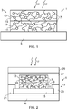
- Fig. 1 schematically illustrates an apparatus 1 according to examples of the disclosure.
- the apparatus 1 comprises a GFET 3 comprising a graphene channel 5 and quantum dots 7 provided overlaying the graphene channel 5.
- the graphene channel 5 may comprise a thin layer of graphene. In some examples the graphene channel 5 may have a thickness in the range of nanometers. In some examples the graphene channel 5 may comprise an atomic monolayer of graphene.
- the quantum dots 7 are coupled to the graphene channel 5.
- the quantum dots 7 may be coupled to the graphene channel 5 so as to enable charge transfer from the quantum dots to the graphene channel 5.
- the quantum dots 7 are provided overlaying the graphene channel 5.
- the quantum dots 7 are provided in a plurality of layers. In the example of Fig. 1 the quantum dots 7 are provided in a first layer 9 and a second layer 13. The second layer 13 is provided overlaying the first layer 9 so that the first layer 9 is positioned between the graphene channel 5 and the second layer 13. In other examples more than two layers of quantum dots 7 may be provided.
- the quantum dots 7 may comprise semiconductor nanocrystals in which there is quantum confinement in all three dimensions.
- the quantum dots 7 may comprise any suitable semiconductor material.
- the semiconductor material that is used for the quantum dots 7 may be chosen to enable incident light to be detected.
- the quantum dots 7 may comprise lead sulphide, cadmium sulphide, cadmium selenide, or any other suitable material.
- the same semiconductor material may be used for the quantum dots 7 in each of the layers 9, 13 within the apparatus 1. In other examples different materials could be used for different layers 9, 13.
- the material and/or dimensions of the quantum dots 7 may be selected to optimise the wavelength of light that is detected by the GFET 3. For example where lead sulphide quantum dots 7 are used the quantum dots 7 may have a size of around 3nm. Other dimensions may be used in other examples.
- the quantum dots 7 may be any suitable shape.
- the quantum dots 7 could be spherical, rods, two dimensional shapes or any other suitable shape. Different shapes of quantum dots could be used in the different layers 9, 13
- the quantum dots 7 are connected to ligands 11, 15.
- a first ligand 11 is connected to the quantum dots 7 and in the second layer 13 of quantum dots a second ligand 15 is connected to the quantum dots 7.
- the first ligand 11 and the second ligand 15 may be different ligands so that the different layers 9, 13 of quantum dots 7 have different refractive indices.
- the different ligands may comprise different materials.
- the different ligands may comprise different ligand coverage levels or any other suitable differences.
- the ligands 11, 15 may be configured to connect the quantum dots 7 to each other.
- the ligands 11, 15 may also be configured to connect the quantum dots 7 to the graphene channel 5.
- the layers 9, 13 of quantum dots 7 may comprise more than one ligand.
- the first layer 9 could comprise a combination of two or more ligands and the second layer 13 could comprise a different combination of ligands.
- the ligands 11, 15 may comprise any suitable material.
- the material or materials that are used for the ligands 11, 15 may be chosen dependent upon the refractive index that is needed, the materials used for the quantum dots 7 or any other suitable factor.
- the ligands 11, 15 may comprise alkanedithiol; where the alkane comprises methane, ethane, propane, butane or any other suitable alkane; alkanethiol; amine such as butylamine; pyridine or any other suitable material.
- the quantum dots 7 may be arranged to sense incident light 17. In some examples the quantum dots 7 may generate excitons in response to incident light 17. The excitons may be separated into electron-hole pairs and either the holes or electrons may be transferred from the quantum dots 7 to the graphene channel 5. This provides a doping effect in the graphene channel 5 so that the output of the apparatus 1 is indicative of the incident light 17.
- the thickness of the layers 9, 13 of quantum dots 7 may be configured to allow for optimal charge transfer from the quantum dots 7 to the graphene channel 5. In some examples the total thickness of the combined layers of quantum dots 7 may be between 50 and 500nm. The thickness that is used may depend on the materials that are used for the quantum dots 7 and the ligands 11, 15 and/or the wavelength of light that is to be detected and/or any other suitable factor.
- the thickness of at least some of the layers of quantum dots 7 may be configured to provide an anti-reflective coating.
- the thickness of the second layer 13 of quantum dots 7 may be configured to provide an anti-reflective coating.
- the thickness that is needed to provide an anti-reflective coating may depend on the refractive indices of the respective layers 9, 13, the wavelength of light 17 that is to be detected and any other suitable factors.
- the second layer 13 of quantum dots 7 acts both as an anti-reflective coating to reduce the amount of light 17 reflected by the apparatus 1 and also as a transducer to convert at least some of the incident light into an electrical response.
- any one or more of the upper layers may act as both an anti-reflective coating and also as a transducer.
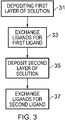
- Fig. 2 illustrates another apparatus according to examples of the disclosure.
- the apparatus 1 of Fig. 2 also comprises a GFET 3 comprising a graphene channel 5 and a plurality of layers 9, 13 of quantum dots 7 which may be as described above.
- the graphene channel 5 extends between a source electrode 21 and a drain electrode 23.
- the graphene channel 5 and the source electrode 21 and drain electrode 23 may be provided on a flexible substrate 25. This may enable a flexible apparatus 1 to be provided.
- the quantum dots 7 are provided overlaying the graphene channel 5 in a plurality of layers 9, 13 where each layer comprises a different ligand 11, 15 or combination of ligands.
- the plurality of layers 9, 13 may be as described above.
- the apparatus 1 comprises two layers 9, 13 of quantum dots 7. It is to be appreciated that more than two layers 9, 13 could be provided in other examples of the disclosure.
- an encapsulating layer 27 is provided overlaying the GFET 3.
- the encapsulating layer 27 is provided overlaying both the graphene channel 5 and the quantum dots 7.
- the encapsulating layer 27 may be configured to act as a barrier to protect the GFET 3 from contaminants such as water, oxygen or other chemicals.
- the encapsulating layer 27 may comprise any suitable material.
- the encapsulating layer 27 may comprise an organic or hybrid organic-inorganic polymer material such as siloxanes, epoxy, acrylic polymers or any other suitable materials. These may be suitable for use in flexible apparatus 1. Other materials may be used in other examples of the disclosure.
- the encapsulating layer 27 may be transparent or at least partially transparent to light 17 of the wavelengths that are to be detected by the GFET 3.
- the encapsulating layer 27 may have a different refractive index to the layers 9, 13 of quantum dots 7.
- the reflective indices and the thickness of the layers 9, 13 of quantum dots 7 may be configured to reduce the reflection of light 17.
- the encapsulating layer 27 may be an adhesive.
- the adhesive may enable additional components to be coupled to the GFET 3.
- a transparent layer 29 is attached to the adhesive 27.
- the transparent layer 29 may comprise glass or any other suitable material.
- the transparent layer 29 may act as a barrier layer to protect the GFET 3.
- the transparent layer 29 may be configured to direct or focus incident light onto the GEFT 3.
- the ligands used in the respective layers 9, 13 of quantum dots may be selected to reduce the reflection of incident light at the boundary between the encapsulating layer 27 and the layers of quantum dots 7. This may increase the proportion of light that reaches the quantum dots 7 and may provide for a more efficient photodetector apparatus 1.
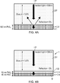
- Fig. 3 illustrates an example method. The method may be used to form apparatus 1 such as the apparatus 1 of Figs. 1 and 2 .
- the method comprises, at block 31, depositing a first layer of quantum dot solution onto a graphene channel 5 of a GFET 3.
- the graphene channel 5 may be provided on a flexible substrate 25 as described above.
- the quantum dot solution may comprise quantum dots 7 connected to a long chain ligand.
- the long chain ligand may be selected to enable the quantum dots 7 to be dissolved in the solution and prevent the quantum dots 7 from precipitating out of the solution.
- the quantum dot solution may be deposited using any suitable deposition process such as ink jet printing or any other suitable technique.
- the ligand exchange replaces the long chain ligand with the first ligand 11.
- the first ligand 11 may be a short chain ligand.
- the first ligand may be a short chain ligand which enables efficient charge transfer from the quantum dots 7 to the graphene channel 5.
- the ligand solution may be solidified to form the first layer 9 of quantum dots 7.
- Any suitable process, such as UV (ultra violet) curing may be used to enable solidification of the quantum dot solution.
- the GEFT 3 may be rinsed to remove the long chain ligand that has been replaced. This may prepare the surface of the GFET 3 for the forming of another layer of quantum dots 7.
- the method comprises depositing a second layer of quantum dot solution overlaying the first layer 9 of quantum dots 7.
- the quantum dot solution may be the same as the quantum dot solution used to create the first layer 9 of quantum dots 7 and may comprise the same type of quantum dots 7 connected to the same long chain ligand. In other examples a different solution comprising different quantum dots 7 and/or a different long chain ligand may be used.
- the quantum dot solution may be deposited using any suitable deposition process such as printing.
- the second ligand exchange may replace the long chain ligand of the solution with the second ligand 15.
- the second ligand 15 may be a short chain ligand which is different to the first ligand11 used in the first layer 9.
- the second ligand 15 may be selected to enable efficient charge transfer from the quantum dots 7 to the graphene channel 5.
- the second ligand 15 may be selected so that the second layer 13 of quantum dots 7 has a different refractive index to the first layer 9 of quantum dots 7.
- the ligand solution may be solidified to form the second layer 13 of quantum dots 7.
- Any suitable process, such as UV (ultra violet) curing may be used to enable solidification of the quantum dot solution.
- the GEFT 3 may be rinsed to remove the long chain ligand that has been replaced by the second ligand exchange process.
- the encapsulating layer 27 may be provided overlaying the second layer 13.
- a further transparent layer 29 may then be provided over the encapsulating layer.
- two different layers 9, 13 of quantum dots 7 are formed. In other examples more than two layers of quantum dots 7 could be formed.
- the additional layers could be provided by depositing further layers of quantum dot solution overlaying the second layer and performing further ligand exchange processes.
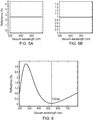
- Figs. 4A and 4B illustrates example layers of quantum dots 7 and example refractive indices.
- the example of Fig. 4A illustrates a single layer 41 of quantum dots 7 and an encapsulating layer 27.
- Fig. 4B illustrates a plurality of layers 9, 13 of quantum dots 7 and an encapsulating layer 27 according to examples of the disclosure. This shows the difference in the amount of light that is reflected with the two different configurations of quantum dots 7.
- the quantum dots 7 are provided in a single layer 41.
- the same ligand or combination of ligands is used throughout the layer 41 of quantum dots 7 so that the single layer 41 has a constant refractive index.
- the single layer 41 of quantum dots 7 may comprise lead sulphide quantum dots 7 having a diameter of around 3nm.
- the single layer 41 of quantum dots may be formed using a NH 4 SCN, mercaptopropionic ligand exchange process.
- the single layer 41 of quantum dots 7 has a refractive index of 2.8.
- the single layer 41 of quantum dots 7 has a thickness of 100nm.
- the thickness of the single layer 41 may be selected to optimize the absorption of incident light and the transfer of charge from the quantum dots 7 to the graphene channel 5 in response to the incident light 17.
- An encapsulating layer 27 is provided overlaying the single layer 41 of quantum dots 7.
- the encapsulating layer 27 may be provided in a much thicker layer than the quantum dots 7.
- the encapsulating layer 27 may comprise an adhesive or any other suitable material.
- the encapsulating layer 27 has a different refractive index to the single layer 41 of quantum dots 7. In the example of Fig. 4A the encapsulating layer 27 has a refractive index of 1.975. Other types of encapsulating layer 27 could be used in other arrangements and these may have different refractive indices.
- the difference in the refractive indices at the boundary between the encapsulating layer 27 and the single layer 41 of quantum dots 7 causes some of the incident light 17 to be reflected at the boundary.
- the incident light has a wavelength of 530nm and 3% of the incident light is reflected.
- the quantum dots 7 also comprise lead sulphide.
- the quantum dots 7 are provided in a first layer 9 and a second layer 13.
- the second layer 13 is provided overlaying the first layer 9.
- Different ligands 11, 15 are used in the different layers 9, 13 so that the first layer 9 has a different refractive index to the second layer 13.
- the first layer 9 of quantum dots 7 comprises lead sulphide quantum dots 7 having a diameter of around 3nm.
- the first layer 9 of quantum dots 7 may be formed using a NH 4 SCN, mercaptopropionic ligand exchange process.
- the second layer 13 of quantum dots 7 also comprise lead sulphide quantum dots 7 having a diameter of around 3nm.
- the second layer 13 of quantum dots 7 may be formed using a 1,3 BDT, benzenedithiol ligand exchange process.
- the first layer 9 has a refractive index of 2.8 and the second layer 13 has a refractive index of 2.4.
- the different layers 9, 13 of quantum dots 7 also have different thicknesses.
- the first layer 9 has a thickness of 45nm and the second layer 13 has a thickness of 55nm. This may provide a total thickness for combined layers 9, 13 of quantum dots of 100nm. This total thickness may be selected to optimize the absorption of incident light and the transfer of charge from the quantum dots to the graphene channel 5 in response to the incident light.
- the different thickness of the different layers 9, 13 may be selected to optimize the amount of light that is reflected by the apparatus 1.
- the example apparatus 1 of Fig. 4B also comprises an encapsulating layer 27 overlaying the layers 9, 13 of quantum dots 7.
- the encapsulating layer 27 may be the same as the encapsulating layer 27 of Fig. 4A and may have a refractive index of 1.975. Other types of encapsulating layer 27 may be used in other examples of the disclosure.
- the difference in the refractive indices at the boundary between the encapsulating layer 27 and the second layer 13 of quantum dots 7 is reduced compared to the example of Fig. 4A . This reduces the amount of incident light 17 that is reflected at the boundary.
- the thickness of the second layer 13 of quantum dots 7 may be selected to reduce the amount of incident light 17 that is reflected.
- the thickness of the second layer 13 of quantum dots 7 may be selected so that for light of a particular wavelength none of the incident light 17 is reflected.
- the thickness of the second layer 13 of quantum dots may be configured to create destructive interference for light path interactions at the boundary between the second layer 13 of quantum dots 7 and the encapsulating layer 27.
- the thickness of the second layer 13 of quantum dots 7 may be proportional to the wavelength of the incident light 17 and the refractive index of the second layer 13.
- ⁇ is the wavelength of the incident light and n 2 is the refractive index of the second layer 13 of quantum dots 7.
- the ligand 15 that is used for the second layer 13 of quantum dots 7 may be selected to provide a desired refractive index.
- n 1 is the refractive index of the first layer 9 of quantum dots 7 and the n e is the refractive index of the encapsulating layer 27.
- the destructive interference is achieved by having the thickness of the second layer 13 of quantum dots 7 as 55nm and refractive index of 2.4.
- the optimal overall thickness of the combined layers 9, 13 of quantum dots is around 100nm this requires a thickness for the first layer 9 of quantum dots 7 of 45nm.
- this reduces the amount of incident light 17 that is reflected to zero and provides a more efficient apparatus 1 compared to the example of Fig. 4A .
- other thickness of the layers 9, 13 and refractive indices may be used in other examples of the disclosure.
- the materials that are used for the ligands 11, 15 may be selected to obtain the desired refractive indices.
- Figs. 5A and 5B illustrate reflectance spectra of layers 9, 13 of quantum dots 7.
- the reflectance spectra were obtained using finite element simulations to calculate the percentage of reflectance R% of a single layer of quantum dots 7.
- the layer of quantum dots 7 was a 100nm thick layer of lead sulphide quantum dots 7 for both the spectra of Fig. 5A and Fig. 5B .
- a refractive index of 2.8 was used and in the reflectance spectrum of Fig. 5B a refractive index of 2.4 was used.
- the different values of the refractive indices were selected using the equations described above.
- the reflectance spectrum of Fig. 5A shows a percentage of reflectance R% of approximately 3% for a refractive index of 2.8.
- the reflectance spectrum of Fig. 5B shows a percentage of reflectance R% of approximately 1 % for a refractive index of 2.4. This shows that the difference between the refractive indices of the encapsulation layer 27 and the quantum dots 7 may be decreased by using different types of ligands for the quantum dots 7. This may enable the second layer 13 of quantum dots 7 to be configured as an antireflective coating.
- Fig. 6 illustrates an example reflectance spectrum for an apparatus such as the apparatus of Figs. 1, 2 and 4B .
- the reflectance spectrum of Fig. 6 was obtained for an apparatus having a first layer 9 of quantum dots 7 of thickness 45nm with refractive index 2.8, a second layer 13 of quantum dots 7 of thickness 55nm with refractive index 2.4 and an encapsulating layer 27 with a refractive index of 1.975.
- This configuration has reduced the percentage of reflectance R% to approximately 0 for a wavelength of 530nm.
- the reflectance spectrum of Fig. 6 shows that the percentage of reflectance R% may be optimized for a wavelength of 530nm so that all of this light reaches the quantum dots 7. This may increase the efficiency of the apparatus 1. It is to be appreciated that the apparatus 1 could be tuned to optimize the percentage of reflectance R% for different wavelengths in other examples of the disclosure.
- the reflectance spectrum of Fig. 6 also shows that the percentage of reflectance R% may be increased for other wavelengths of light. This may enable incident light 17 of wavelengths that are not of interest to be reflected. In the example of Fig. 6 the percentage of reflectance R% is increased in the UV spectrum. This may be beneficial as UV light may be used to cure the layers 9, 13 of quantum dots 7. Having the layers of quantum dots 7 configured to reflect the UV light may protect the underlying layers from damage from the UV light during the curing process.
- the encapsulation layer 27 has been an adhesive with a refractive index of 1.975.
- Other types of encapsulation layer 27 may be used in other examples. This may require different refractive indices and/or thicknesses for the layers 9, 13 of quantum dots.
- aluminium oxide could be used as the encapsulation layer 27.
- This has a refractive index of approximately 1.77 for light with a wavelength of 530nm.
- the second layer 13 of quantum dots 7 may be arranged to have a refractive index of 2.23.
- the different refractive index may be obtained using a different type of ligand or a different combination of ligands and/or different levels of ligand coverage.
- Fig. 7 illustrates an example energy diagram which shows trap mediated charge transfer of holes and electrons between a graphene channel 5 and different layers 9, 13 of quantum dots 7.
- the ligands 11, 15 enable charge transfer from the quantum dots 7 to the graphene channel 5 the use of different ligands will affect the efficiency at which charge is transferred as well as the percentage of incident light 17 that is reflected.
- Charges may be transferred from the quantum dots 7 to the graphene channel 5 by two different mechanisms.
- the first mechanism is band mediated and requires alignment of the energy bands within the different layers 9, 13 of the quantum dots 7.
- the second mechanism is trap mediated. This requires hopping and tunneling of charges between the trap sites. This is illustrated in Fig. 7 .
- Fig. 7 shows the energy levels for the graphene channel, the first layer 9 of quantum dots 7 and the second layer 13 of quantum dots 7.
- the first layer 9 comprises lead sulphide quantum dots 7 and an NH 4 SCN terminated ligand and the second layer 13 comprises lead sulphide quantum dots 7 and a BDT terminated ligand.
- the incident light 17 generates electron-hole pairs in both the first layer 9 of quantum dots 7 and the second layer 13 of quantum dots 7.
- the energetically favorable holes pass from the second layer 13 of quantum dots 7 to the first layer 9 of quantum dots 7.
- the electrons move in the opposite direction so that the electrons pass from the first layer 9 to the second layer 13.
- the holes will then pass from the first layer 9 of quantum dots 7 to the graphene channel 5.
- Fig. 7 shows that there is a small barrier for hole transport from the first layer 9 of quantum dots 7 to the graphene channel 5. This ensures that charges can be transferred from the quantum dots 7 to the graphene channel 5 even when the quantum dots 7 are provided in a plurality of layers.
- Examples of the disclosure provide an apparatus 1 that may be used as a photodetector.
- the quantum dots 7 By providing the quantum dots 7 in a plurality of layers 9, 13 one or more of the layers can act as an antireflective coating which reduces the percentage of incident light 17 reflected by the apparatus 1. This provides for a more efficient photodetector.
- one or more of the layers of quantum dots acts both as an anti reflective coating and as a transducer. This provides an improved photodetector as there is no need to provide additional layers of antireflective coating. This may enable the overall thickness of the apparatus 1 to be minimized as there is no need to introduce the additional anti-reflective layers. Also as there is no need for the additional anti-reflective layers this may make the apparatus 1 easier to fabricate as there is no need to add additional anti-reflective layers.
- Examples of the disclosure may enable the reflectance of the light to be optimized for a particular wavelength by selecting appropriate refractive indices and thickness of the layers 9, 13 of quantum dots 7. This may enable the apparatus 1 to be optimized for detecting a particular wavelength or range of wavelengths of light.
- the total thickness of the combined layers 9, 13 of quantum dots maybe kept at an optimum level for absorption of incident light because the anti-reflective properties can be provided by varying the thickness of layers of the quantum dots 7.
- example or “for example” or “may” in the text denotes, whether explicitly stated or not, that such features or functions are present in at least the described example, whether described as an example or not, and that they can be, but are not necessarily, present in some of or all other examples.
- example “for example” or “may” refers to a particular instance in a class of examples.
- a property of the instance can be a property of only that instance or a property of the class or a property of a subclass of the class that includes some but not all of the instances in the class. It is therefore implicitly disclosed that a feature described with reference to one example but not with reference to another example, can where possible be used in that other example but does not necessarily have to be used in that other example.
Landscapes
- Engineering & Computer Science (AREA)
- Chemical & Material Sciences (AREA)
- Nanotechnology (AREA)
- Crystallography & Structural Chemistry (AREA)
- Theoretical Computer Science (AREA)
- Physics & Mathematics (AREA)
- Mathematical Physics (AREA)
- Health & Medical Sciences (AREA)
- Life Sciences & Earth Sciences (AREA)
- General Health & Medical Sciences (AREA)
- Molecular Biology (AREA)
- Light Receiving Elements (AREA)
- Thin Film Transistor (AREA)
- Microelectronics & Electronic Packaging (AREA)
Abstract
Description
- Examples of the disclosure relate to an apparatus and method of forming an apparatus comprising a graphene field effect transistor. In particular, they relate to an apparatus and method of forming an apparatus comprising a graphene field effect transistor where the graphene field effect transistor comprises quantum dots.
- Graphene field effect transistors (GFETs) and quantum dot-graphene field effect transistors (QD-GFETs) may be used as photodetectors and transduce incident light into a measurable electrical response. It is useful to increase the efficiency of such devices.
- According to various, but not necessarily all, examples of the disclosure there may be provided an apparatus comprising: a graphene field effect transistor where the graphene field effect transistor comprises a graphene channel and quantum dots provided overlaying the graphene channel, wherein the quantum dots comprise a first layer comprising quantum dots connected to a first ligand and a second layer comprising quantum dots connected to a second ligand, and wherein the first ligand is configured to cause the first layer to have a first refractive index and the second ligand is configured to cause the second layer to have a second refractive index wherein the second refractive index is different to the first refractive index.
- The quantum dots may comprise more than two layers and different ligands may be used in different layers.
- The thickness of at least one of the layers of quantum dots may be arranged to provide an anti-reflective coating. The layers arranged to provide an anti-reflective coating may also be arranged to transduce incident light into an electrical output.
- The total thickness of the layers of quantum dots may be between 10-500nm.
- The apparatus may comprise an encapsulating layer overlaying the graphene field effect transistor. The encapsulating layer may comprise an organic material. The encapsulating layer may comprise an adhesive. The apparatus may comprise a transparent layer attached to the adhesive.
- According to various, but not necessarily all, examples of the disclosure there may be provided a photodetector comprising at least one apparatus according to any preceding claim.
- According to various, but not necessarily all, examples of the disclosure there may be provided a method comprising: depositing a first layer of quantum dot solution onto a graphene channel of a graphene field effect transistor; exchanging ligands to form a first layer of quantum dots connected to a first ligand; depositing a second layer of quantum dot solution overlaying the first layer of quantum dots; and exchanging ligands to form a second layer of quantum dots connected to a second ligand.
- The method may comprise depositing further layers of quantum dot solution and exchanging ligands to provide further layers of quantum dots connected to ligands.
- Exchanging ligands may comprise exchanging a longer ligand for a shorter ligand.
- Different ligands may be used in different layers of quantum dots.
- The thickness of at least one of the layers of quantum dots is arranged to provide an anti-reflective coating. The layers arranged to provide an anti-reflective coating may also be arranged to transduce incident light into an electrical output.
- The total thickness of the layers of quantum dots may be between 10-500nm.
- The method may comprise providing an encapsulating layer overlaying the graphene field effect transistor. The encapsulating layer may comprise an organic material. The encapsulating layer may comprise an adhesive. The method may comprise providing a transparent layer attached to the adhesive.
- According to various, but not necessarily all, examples of the disclosure there is provided examples as claimed in the appended claims.
- For a better understanding of various examples that are useful for understanding the detailed description, reference will now be made by way of example only to the accompanying drawings in which:
-
Fig. 1 illustrates an apparatus; -
Fig. 2 illustrates another apparatus according to examples of the disclosure; -
Fig. 3 illustrates a method; -
Fig. 4 illustrates example layers of quantum dots; -
Figs. 5A and 5B illustrate reflectance spectra of layers of quantum dots; -
Fig. 6 illustrates an example reflectance spectrum; and -
Fig. 7 illustrates an example energy diagram. - The Figures illustrate an
apparatus 1 comprising: a graphenefield effect transistor 3 where the graphenefield effect transistor 3 comprises agraphene channel 5 andquantum dots 7 provided overlaying thegraphene channel 5, wherein thequantum dots 7 comprise afirst layer 9 comprisingquantum dots 7 connected to afirst ligand 11 and asecond layer 13 comprisingquantum dots 7 connected to asecond ligand 15, and wherein thefirst ligand 11 is configured to cause thefirst layer 9 to have a first refractive index and thesecond ligand 15 is configured to cause thesecond layer 13 to have a second refractive index wherein the second refractive index is different to the first refractive index. - The
apparatus 1 may be used as a photodetector. Thelayers quantum dots 7 may be arranged to detect incident light and transduce the incident light into an electrical output. -
Fig. 1 schematically illustrates anapparatus 1 according to examples of the disclosure. Theapparatus 1 comprises aGFET 3 comprising agraphene channel 5 andquantum dots 7 provided overlaying thegraphene channel 5. - The
graphene channel 5 may comprise a thin layer of graphene. In some examples thegraphene channel 5 may have a thickness in the range of nanometers. In some examples thegraphene channel 5 may comprise an atomic monolayer of graphene. - The
quantum dots 7 are coupled to thegraphene channel 5. Thequantum dots 7 may be coupled to thegraphene channel 5 so as to enable charge transfer from the quantum dots to thegraphene channel 5. - The
quantum dots 7 are provided overlaying thegraphene channel 5. Thequantum dots 7 are provided in a plurality of layers. In the example ofFig. 1 thequantum dots 7 are provided in afirst layer 9 and asecond layer 13. Thesecond layer 13 is provided overlaying thefirst layer 9 so that thefirst layer 9 is positioned between thegraphene channel 5 and thesecond layer 13. In other examples more than two layers ofquantum dots 7 may be provided. - The
quantum dots 7 may comprise semiconductor nanocrystals in which there is quantum confinement in all three dimensions. Thequantum dots 7 may comprise any suitable semiconductor material. The semiconductor material that is used for thequantum dots 7 may be chosen to enable incident light to be detected. In some examples thequantum dots 7 may comprise lead sulphide, cadmium sulphide, cadmium selenide, or any other suitable material. - In some examples the same semiconductor material may be used for the
quantum dots 7 in each of thelayers apparatus 1. In other examples different materials could be used fordifferent layers - The material and/or dimensions of the
quantum dots 7 may be selected to optimise the wavelength of light that is detected by theGFET 3. For example where lead sulphidequantum dots 7 are used thequantum dots 7 may have a size of around 3nm. Other dimensions may be used in other examples. - The
quantum dots 7 may be any suitable shape. Thequantum dots 7 could be spherical, rods, two dimensional shapes or any other suitable shape. Different shapes of quantum dots could be used in thedifferent layers - In the
example apparatus 1 ofFig. 1 thequantum dots 7 are connected to ligands 11, 15. In thefirst layer 9 of quantum dots 7 afirst ligand 11 is connected to thequantum dots 7 and in thesecond layer 13 of quantum dots asecond ligand 15 is connected to thequantum dots 7. Thefirst ligand 11 and thesecond ligand 15 may be different ligands so that thedifferent layers quantum dots 7 have different refractive indices. In some examples the different ligands may comprise different materials. In some examples the different ligands may comprise different ligand coverage levels or any other suitable differences. - The
ligands quantum dots 7 to each other. Theligands quantum dots 7 to thegraphene channel 5. - In some examples of the disclosure the
layers quantum dots 7 may comprise more than one ligand. For instance thefirst layer 9 could comprise a combination of two or more ligands and thesecond layer 13 could comprise a different combination of ligands. - The
ligands ligands quantum dots 7 or any other suitable factor. In some examples theligands - The
quantum dots 7 may be arranged tosense incident light 17. In some examples thequantum dots 7 may generate excitons in response toincident light 17. The excitons may be separated into electron-hole pairs and either the holes or electrons may be transferred from thequantum dots 7 to thegraphene channel 5. This provides a doping effect in thegraphene channel 5 so that the output of theapparatus 1 is indicative of theincident light 17. - The thickness of the
layers quantum dots 7 may be configured to allow for optimal charge transfer from thequantum dots 7 to thegraphene channel 5. In some examples the total thickness of the combined layers ofquantum dots 7 may be between 50 and 500nm. The thickness that is used may depend on the materials that are used for thequantum dots 7 and theligands - The thickness of at least some of the layers of
quantum dots 7 may be configured to provide an anti-reflective coating. In the example ofFig. 1 the thickness of thesecond layer 13 ofquantum dots 7 may be configured to provide an anti-reflective coating. The thickness that is needed to provide an anti-reflective coating may depend on the refractive indices of therespective layers - In such examples the
second layer 13 ofquantum dots 7 acts both as an anti-reflective coating to reduce the amount of light 17 reflected by theapparatus 1 and also as a transducer to convert at least some of the incident light into an electrical response. In examples where more than twolayers -
Fig. 2 illustrates another apparatus according to examples of the disclosure. Theapparatus 1 ofFig. 2 also comprises aGFET 3 comprising agraphene channel 5 and a plurality oflayers quantum dots 7 which may be as described above. - The
graphene channel 5 extends between asource electrode 21 and adrain electrode 23. Thegraphene channel 5 and thesource electrode 21 anddrain electrode 23 may be provided on aflexible substrate 25. This may enable aflexible apparatus 1 to be provided. - The
quantum dots 7 are provided overlaying thegraphene channel 5 in a plurality oflayers different ligand layers Fig. 2 theapparatus 1 comprises twolayers quantum dots 7. It is to be appreciated that more than twolayers - In the
example apparatus 1 ofFig. 2 anencapsulating layer 27 is provided overlaying theGFET 3. The encapsulatinglayer 27 is provided overlaying both thegraphene channel 5 and thequantum dots 7. The encapsulatinglayer 27 may be configured to act as a barrier to protect theGFET 3 from contaminants such as water, oxygen or other chemicals. - The encapsulating
layer 27 may comprise any suitable material. In some examples theencapsulating layer 27 may comprise an organic or hybrid organic-inorganic polymer material such as siloxanes, epoxy, acrylic polymers or any other suitable materials. These may be suitable for use inflexible apparatus 1. Other materials may be used in other examples of the disclosure. - The encapsulating
layer 27 may be transparent or at least partially transparent to light 17 of the wavelengths that are to be detected by theGFET 3. The encapsulatinglayer 27 may have a different refractive index to thelayers quantum dots 7. The reflective indices and the thickness of thelayers quantum dots 7 may be configured to reduce the reflection oflight 17. - In some examples the
encapsulating layer 27 may be an adhesive. The adhesive may enable additional components to be coupled to theGFET 3. In the example ofFig. 2 atransparent layer 29 is attached to the adhesive 27. Thetransparent layer 29 may comprise glass or any other suitable material. Thetransparent layer 29 may act as a barrier layer to protect theGFET 3. In some examples thetransparent layer 29 may be configured to direct or focus incident light onto theGEFT 3. - In the example apparatus of
Fig. 2 the ligands used in therespective layers layer 27 and the layers ofquantum dots 7. This may increase the proportion of light that reaches thequantum dots 7 and may provide for a moreefficient photodetector apparatus 1. -
Fig. 3 illustrates an example method. The method may be used to formapparatus 1 such as theapparatus 1 ofFigs. 1 and 2 . - The method comprises, at
block 31, depositing a first layer of quantum dot solution onto agraphene channel 5 of aGFET 3. Thegraphene channel 5 may be provided on aflexible substrate 25 as described above. - The quantum dot solution may comprise
quantum dots 7 connected to a long chain ligand. The long chain ligand may be selected to enable thequantum dots 7 to be dissolved in the solution and prevent thequantum dots 7 from precipitating out of the solution. - The quantum dot solution may be deposited using any suitable deposition process such as ink jet printing or any other suitable technique.
- Once the quantum dot solution has been deposited a ligand exchange process is carried out at
block 33. The ligand exchange replaces the long chain ligand with thefirst ligand 11. Thefirst ligand 11 may be a short chain ligand. The first ligand may be a short chain ligand which enables efficient charge transfer from thequantum dots 7 to thegraphene channel 5. - Once the ligand exchange process has been carried out the ligand solution may be solidified to form the
first layer 9 ofquantum dots 7. Any suitable process, such as UV (ultra violet) curing may be used to enable solidification of the quantum dot solution. - Once the
first layer 9 ofquantum dots 7 has been formed theGEFT 3 may be rinsed to remove the long chain ligand that has been replaced. This may prepare the surface of theGFET 3 for the forming of another layer ofquantum dots 7. - At
block 35 the method comprises depositing a second layer of quantum dot solution overlaying thefirst layer 9 ofquantum dots 7. The quantum dot solution may be the same as the quantum dot solution used to create thefirst layer 9 ofquantum dots 7 and may comprise the same type ofquantum dots 7 connected to the same long chain ligand. In other examples a different solution comprisingdifferent quantum dots 7 and/or a different long chain ligand may be used. The quantum dot solution may be deposited using any suitable deposition process such as printing. - Once the quantum dot solution has been deposited a second ligand exchange process is carried out at
block 37. The second ligand exchange may replace the long chain ligand of the solution with thesecond ligand 15. Thesecond ligand 15 may be a short chain ligand which is different to the first ligand11 used in thefirst layer 9. Thesecond ligand 15 may be selected to enable efficient charge transfer from thequantum dots 7 to thegraphene channel 5. Thesecond ligand 15 may be selected so that thesecond layer 13 ofquantum dots 7 has a different refractive index to thefirst layer 9 ofquantum dots 7. - Once the ligand exchange process has been carried out the ligand solution may be solidified to form the
second layer 13 ofquantum dots 7. Any suitable process, such as UV (ultra violet) curing may be used to enable solidification of the quantum dot solution. - Once the
second layer 13 ofquantum dots 7 has been formed theGEFT 3 may be rinsed to remove the long chain ligand that has been replaced by the second ligand exchange process. - Once the
second layer 13 ofquantum dots 7 has been formed theencapsulating layer 27 may be provided overlaying thesecond layer 13. A furthertransparent layer 29 may then be provided over the encapsulating layer. - In the example method of
Fig. 3 twodifferent layers quantum dots 7 are formed. In other examples more than two layers ofquantum dots 7 could be formed. The additional layers could be provided by depositing further layers of quantum dot solution overlaying the second layer and performing further ligand exchange processes. -
Figs. 4A and 4B illustrates example layers ofquantum dots 7 and example refractive indices. The example ofFig. 4A illustrates asingle layer 41 ofquantum dots 7 and anencapsulating layer 27.Fig. 4B illustrates a plurality oflayers quantum dots 7 and anencapsulating layer 27 according to examples of the disclosure. This shows the difference in the amount of light that is reflected with the two different configurations ofquantum dots 7. - In the example of
Fig. 4A thequantum dots 7 are provided in asingle layer 41. The same ligand or combination of ligands is used throughout thelayer 41 ofquantum dots 7 so that thesingle layer 41 has a constant refractive index. - In the example of
Fig. 4A thesingle layer 41 ofquantum dots 7 may comprise leadsulphide quantum dots 7 having a diameter of around 3nm. Thesingle layer 41 of quantum dots may be formed using a NH4SCN, mercaptopropionic ligand exchange process. Thesingle layer 41 ofquantum dots 7 has a refractive index of 2.8. - In the example of
Fig. 4A thesingle layer 41 ofquantum dots 7 has a thickness of 100nm. The thickness of thesingle layer 41 may be selected to optimize the absorption of incident light and the transfer of charge from thequantum dots 7 to thegraphene channel 5 in response to theincident light 17. - An
encapsulating layer 27 is provided overlaying thesingle layer 41 ofquantum dots 7. The encapsulatinglayer 27 may be provided in a much thicker layer than thequantum dots 7. The encapsulatinglayer 27 may comprise an adhesive or any other suitable material. The encapsulatinglayer 27 has a different refractive index to thesingle layer 41 ofquantum dots 7. In the example ofFig. 4A the encapsulatinglayer 27 has a refractive index of 1.975. Other types of encapsulatinglayer 27 could be used in other arrangements and these may have different refractive indices. - The difference in the refractive indices at the boundary between the encapsulating
layer 27 and thesingle layer 41 ofquantum dots 7 causes some of the incident light 17 to be reflected at the boundary. In the example ofFig. 4A the incident light has a wavelength of 530nm and 3% of the incident light is reflected. - In the example of
Fig. 4B thequantum dots 7 also comprise lead sulphide. Thequantum dots 7 are provided in afirst layer 9 and asecond layer 13. Thesecond layer 13 is provided overlaying thefirst layer 9.Different ligands different layers first layer 9 has a different refractive index to thesecond layer 13. - The
first layer 9 ofquantum dots 7 comprises leadsulphide quantum dots 7 having a diameter of around 3nm. Thefirst layer 9 ofquantum dots 7 may be formed using a NH4SCN, mercaptopropionic ligand exchange process. Thesecond layer 13 ofquantum dots 7 also comprise leadsulphide quantum dots 7 having a diameter of around 3nm. Thesecond layer 13 ofquantum dots 7 may be formed using a 1,3 BDT, benzenedithiol ligand exchange process. In the example ofFig. 4B thefirst layer 9 has a refractive index of 2.8 and thesecond layer 13 has a refractive index of 2.4. - The
different layers quantum dots 7 also have different thicknesses. In the example ofFig. 4B thefirst layer 9 has a thickness of 45nm and thesecond layer 13 has a thickness of 55nm. This may provide a total thickness for combinedlayers graphene channel 5 in response to the incident light. The different thickness of thedifferent layers apparatus 1. - The
example apparatus 1 ofFig. 4B also comprises anencapsulating layer 27 overlaying thelayers quantum dots 7. The encapsulatinglayer 27 may be the same as theencapsulating layer 27 ofFig. 4A and may have a refractive index of 1.975. Other types of encapsulatinglayer 27 may be used in other examples of the disclosure. - The difference in the refractive indices at the boundary between the encapsulating
layer 27 and thesecond layer 13 ofquantum dots 7 is reduced compared to the example ofFig. 4A . This reduces the amount of incident light 17 that is reflected at the boundary. - The thickness of the
second layer 13 ofquantum dots 7 may be selected to reduce the amount of incident light 17 that is reflected. The thickness of thesecond layer 13 ofquantum dots 7 may be selected so that for light of a particular wavelength none of theincident light 17 is reflected. The thickness of thesecond layer 13 of quantum dots may be configured to create destructive interference for light path interactions at the boundary between thesecond layer 13 ofquantum dots 7 and theencapsulating layer 27. - In order to create the destructive interference the thickness of the
second layer 13 ofquantum dots 7 may be proportional to the wavelength of theincident light 17 and the refractive index of thesecond layer 13. The thickness t of thesecond layer 13 may be given by:
- Where λ is the wavelength of the incident light and n2 is the refractive index of the
second layer 13 ofquantum dots 7. - The
ligand 15 that is used for thesecond layer 13 ofquantum dots 7 may be selected to provide a desired refractive index. The refractive index that is needed is given by:
- Where n1 is the refractive index of the
first layer 9 ofquantum dots 7 and the ne is the refractive index of theencapsulating layer 27. - In the example of
Fig.4B the destructive interference is achieved by having the thickness of thesecond layer 13 ofquantum dots 7 as 55nm and refractive index of 2.4. As the optimal overall thickness of the combinedlayers first layer 9 ofquantum dots 7 of 45nm. In the example ofFig. 4B this reduces the amount of incident light 17 that is reflected to zero and provides a moreefficient apparatus 1 compared to the example ofFig. 4A . It is to be appreciated that other thickness of thelayers - Once the desired refractive index of the
layers ligands -
Figs. 5A and 5B illustrate reflectance spectra oflayers quantum dots 7. The reflectance spectra were obtained using finite element simulations to calculate the percentage of reflectance R% of a single layer ofquantum dots 7. The layer ofquantum dots 7 was a 100nm thick layer of leadsulphide quantum dots 7 for both the spectra ofFig. 5A and Fig. 5B . In the reflectance spectrum ofFig. 5A a refractive index of 2.8 was used and in the reflectance spectrum ofFig. 5B a refractive index of 2.4 was used. The different values of the refractive indices were selected using the equations described above. - The reflectance spectrum of
Fig. 5A shows a percentage of reflectance R% of approximately 3% for a refractive index of 2.8. The reflectance spectrum ofFig. 5B shows a percentage of reflectance R% of approximately 1 % for a refractive index of 2.4. This shows that the difference between the refractive indices of theencapsulation layer 27 and thequantum dots 7 may be decreased by using different types of ligands for thequantum dots 7. This may enable thesecond layer 13 ofquantum dots 7 to be configured as an antireflective coating. -
Fig. 6 illustrates an example reflectance spectrum for an apparatus such as the apparatus ofFigs. 1, 2 and4B . The reflectance spectrum ofFig. 6 was obtained for an apparatus having afirst layer 9 ofquantum dots 7 of thickness 45nm with refractive index 2.8, asecond layer 13 ofquantum dots 7 of thickness 55nm with refractive index 2.4 and anencapsulating layer 27 with a refractive index of 1.975. This configuration has reduced the percentage of reflectance R% to approximately 0 for a wavelength of 530nm. - The reflectance spectrum of
Fig. 6 shows that the percentage of reflectance R% may be optimized for a wavelength of 530nm so that all of this light reaches thequantum dots 7. This may increase the efficiency of theapparatus 1. It is to be appreciated that theapparatus 1 could be tuned to optimize the percentage of reflectance R% for different wavelengths in other examples of the disclosure. - The reflectance spectrum of
Fig. 6 also shows that the percentage of reflectance R% may be increased for other wavelengths of light. This may enableincident light 17 of wavelengths that are not of interest to be reflected. In the example ofFig. 6 the percentage of reflectance R% is increased in the UV spectrum. This may be beneficial as UV light may be used to cure thelayers quantum dots 7. Having the layers ofquantum dots 7 configured to reflect the UV light may protect the underlying layers from damage from the UV light during the curing process. - In the examples described above the
encapsulation layer 27 has been an adhesive with a refractive index of 1.975. Other types ofencapsulation layer 27 may be used in other examples. This may require different refractive indices and/or thicknesses for thelayers encapsulation layer 27. This has a refractive index of approximately 1.77 for light with a wavelength of 530nm. In such examples thesecond layer 13 ofquantum dots 7 may be arranged to have a refractive index of 2.23. The different refractive index may be obtained using a different type of ligand or a different combination of ligands and/or different levels of ligand coverage. -
Fig. 7 illustrates an example energy diagram which shows trap mediated charge transfer of holes and electrons between agraphene channel 5 anddifferent layers quantum dots 7. - As the
ligands quantum dots 7 to thegraphene channel 5 the use of different ligands will affect the efficiency at which charge is transferred as well as the percentage of incident light 17 that is reflected. - Charges may be transferred from the
quantum dots 7 to thegraphene channel 5 by two different mechanisms. The first mechanism is band mediated and requires alignment of the energy bands within thedifferent layers quantum dots 7. - The second mechanism is trap mediated. This requires hopping and tunneling of charges between the trap sites. This is illustrated in
Fig. 7 . -
Fig. 7 shows the energy levels for the graphene channel, thefirst layer 9 ofquantum dots 7 and thesecond layer 13 ofquantum dots 7. In the example ofFig. 7 thefirst layer 9 comprises leadsulphide quantum dots 7 and an NH4SCN terminated ligand and thesecond layer 13 comprises leadsulphide quantum dots 7 and a BDT terminated ligand. - The
incident light 17 generates electron-hole pairs in both thefirst layer 9 ofquantum dots 7 and thesecond layer 13 ofquantum dots 7. - The energetically favorable holes pass from the
second layer 13 ofquantum dots 7 to thefirst layer 9 ofquantum dots 7. The electrons move in the opposite direction so that the electrons pass from thefirst layer 9 to thesecond layer 13. The holes will then pass from thefirst layer 9 ofquantum dots 7 to thegraphene channel 5.Fig. 7 shows that there is a small barrier for hole transport from thefirst layer 9 ofquantum dots 7 to thegraphene channel 5. This ensures that charges can be transferred from thequantum dots 7 to thegraphene channel 5 even when thequantum dots 7 are provided in a plurality of layers. - Examples of the disclosure provide an
apparatus 1 that may be used as a photodetector. By providing thequantum dots 7 in a plurality oflayers apparatus 1. This provides for a more efficient photodetector. - In examples of the disclosure, one or more of the layers of quantum dots acts both as an anti reflective coating and as a transducer. This provides an improved photodetector as there is no need to provide additional layers of antireflective coating. This may enable the overall thickness of the
apparatus 1 to be minimized as there is no need to introduce the additional anti-reflective layers. Also as there is no need for the additional anti-reflective layers this may make theapparatus 1 easier to fabricate as there is no need to add additional anti-reflective layers. - Examples of the disclosure may enable the reflectance of the light to be optimized for a particular wavelength by selecting appropriate refractive indices and thickness of the
layers quantum dots 7. This may enable theapparatus 1 to be optimized for detecting a particular wavelength or range of wavelengths of light. - In the examples of the disclosure the total thickness of the combined
layers quantum dots 7. - The term "comprise" is used in this document with an inclusive not an exclusive meaning. That is any reference to X comprising Y indicates that X may comprise only one Y or may comprise more than one Y. If it is intended to use "comprise" with an exclusive meaning then it will be made clear in the context by referring to "comprising only one..." or by using "consisting".
- In this brief description, reference has been made to various examples. The description of features or functions in relation to an example indicates that those features or functions are present in that example. The use of the term "example" or "for example" or "may" in the text denotes, whether explicitly stated or not, that such features or functions are present in at least the described example, whether described as an example or not, and that they can be, but are not necessarily, present in some of or all other examples. Thus "example", "for example" or "may" refers to a particular instance in a class of examples. A property of the instance can be a property of only that instance or a property of the class or a property of a subclass of the class that includes some but not all of the instances in the class. It is therefore implicitly disclosed that a feature described with reference to one example but not with reference to another example, can where possible be used in that other example but does not necessarily have to be used in that other example.
- Although embodiments of the present invention have been described in the preceding paragraphs with reference to various examples, it should be appreciated that modifications to the examples given can be made without departing from the scope of the invention as claimed.
- Features described in the preceding description may be used in combinations other than the combinations explicitly described.
- Although functions have been described with reference to certain features, those functions may be performable by other features whether described or not.
- Although features have been described with reference to certain embodiments, those features may also be present in other embodiments whether described or not.
- Whilst endeavoring in the foregoing specification to draw attention to those features of the invention believed to be of particular importance it should be understood that the Applicant claims protection in respect of any patentable feature or combination of features hereinbefore referred to and/or shown in the drawings whether or not particular emphasis has been placed thereon.
Claims (15)
- An apparatus comprising:a graphene field effect transistor where the graphene field effect transistor comprises a graphene channel and quantum dots provided overlaying the graphene channel, whereinthe quantum dots comprise a first layer comprising quantum dots connected to a first ligand and a second layer comprising quantum dots connected to a second ligand, and whereinthe first ligand is configured to cause the first layer to have a first refractive index and the second ligand is configured to cause the second layer to have a second refractive index wherein the second refractive index is different to the first refractive index.
- An apparatus as claimed in any preceding claim wherein the quantum dots comprise more than two layers and different ligands are used in different layers.
- An apparatus as claimed in any preceding claim wherein the thickness of at least one of the layers of quantum dots is arranged to provide an anti-reflective coating.
- An apparatus as claimed in claim 3 wherein the layers arranged to provide an anti-reflective coating are also arranged to transduce incident light into an electrical output.
- An apparatus as claimed in any preceding claim wherein the total thickness of the layers of quantum dots is between 10-500nm.
- An apparatus as claimed in any preceding claim comprising an encapsulating layer overlaying the graphene field effect transistor.
- An apparatus as claimed in claim 6 wherein the encapsulating layer comprises an organic material.
- An apparatus as claimed in any of claims 6 to 7 wherein the encapsulating layer comprises an adhesive.
- An apparatus as claimed in claim 8 comprising a transparent layer attached to the adhesive.
- A photodetector comprising at least one apparatus according to any preceding claim.
- A method comprising:depositing a first layer of quantum dot solution onto a graphene channel of a graphene field effect transistor;exchanging ligands to form a first layer of quantum dots connected to a first ligand;depositing a second layer of quantum dot solution overlaying the first layer of quantum dots; andexchanging ligands to form a second layer of quantum dots connected to a second ligand.
- A method as claimed in claim 11 comprising depositing further layers of quantum dot solution and exchanging ligands to provide further layers of quantum dots connected to ligands.
- A method as claimed in any of claims 11 to 12 wherein exchanging ligands comprises exchanging a longer ligand for a shorter ligand.
- A method as claimed in any of claims 11 to 13 wherein different ligands are used in different layers of quantum dots.
- A method as claimed in any of claims 11 to 14 wherein the thickness of at least one of the layers of quantum dots is arranged to provide an anti-reflective coating.
Priority Applications (3)
| Application Number | Priority Date | Filing Date | Title |
|---|---|---|---|
| EP16168160.6A EP3242333B1 (en) | 2016-05-03 | 2016-05-03 | An apparatus and method of forming an apparatus comprising a graphene field effect transistor |
| US16/097,593 US20190157396A1 (en) | 2016-05-03 | 2017-04-20 | An apparatus and method of forming an apparatus comprising a graphene field effect transistor |
| PCT/FI2017/050299 WO2017191356A1 (en) | 2016-05-03 | 2017-04-20 | An apparatus and method of forming an apparatus comprising a graphene field effect transistor |
Applications Claiming Priority (1)
| Application Number | Priority Date | Filing Date | Title |
|---|---|---|---|
| EP16168160.6A EP3242333B1 (en) | 2016-05-03 | 2016-05-03 | An apparatus and method of forming an apparatus comprising a graphene field effect transistor |
Publications (2)
| Publication Number | Publication Date |
|---|---|
| EP3242333A1 true EP3242333A1 (en) | 2017-11-08 |
| EP3242333B1 EP3242333B1 (en) | 2020-09-09 |
Family
ID=55919644
Family Applications (1)
| Application Number | Title | Priority Date | Filing Date |
|---|---|---|---|
| EP16168160.6A Active EP3242333B1 (en) | 2016-05-03 | 2016-05-03 | An apparatus and method of forming an apparatus comprising a graphene field effect transistor |
Country Status (3)
| Country | Link |
|---|---|
| US (1) | US20190157396A1 (en) |
| EP (1) | EP3242333B1 (en) |
| WO (1) | WO2017191356A1 (en) |
Cited By (1)
| Publication number | Priority date | Publication date | Assignee | Title |
|---|---|---|---|---|
| CN110010782A (en) * | 2019-02-28 | 2019-07-12 | 纳晶科技股份有限公司 | A kind of quantum dot light emitting layer and preparation method thereof, quantum dot device |
Families Citing this family (4)
| Publication number | Priority date | Publication date | Assignee | Title |
|---|---|---|---|---|
| US11538948B2 (en) * | 2019-06-26 | 2022-12-27 | University Of South Carolina | Quantum dot photovoltaic junctions |
| JPWO2021002112A1 (en) | 2019-07-01 | 2021-01-07 | ||
| JPWO2021002106A1 (en) * | 2019-07-01 | 2021-01-07 | ||
| WO2024219264A1 (en) * | 2023-04-20 | 2024-10-24 | 富士フイルム株式会社 | Photodetection element, method for manufacturing photodetection element, and image sensor |
Citations (2)
| Publication number | Priority date | Publication date | Assignee | Title |
|---|---|---|---|---|
| US20140126037A1 (en) * | 2008-05-30 | 2014-05-08 | Opalux Incorporated | Tunable bragg stack |
| US20140299741A1 (en) * | 2013-04-05 | 2014-10-09 | Nokia Corporation | Transparent Photodetector for Mobile Devices |
Family Cites Families (27)
| Publication number | Priority date | Publication date | Assignee | Title |
|---|---|---|---|---|
| US6607829B1 (en) * | 1997-11-13 | 2003-08-19 | Massachusetts Institute Of Technology | Tellurium-containing nanocrystalline materials |
| US6322901B1 (en) * | 1997-11-13 | 2001-11-27 | Massachusetts Institute Of Technology | Highly luminescent color-selective nano-crystalline materials |
| US6501091B1 (en) * | 1998-04-01 | 2002-12-31 | Massachusetts Institute Of Technology | Quantum dot white and colored light emitting diodes |
| US6225198B1 (en) * | 2000-02-04 | 2001-05-01 | The Regents Of The University Of California | Process for forming shaped group II-VI semiconductor nanocrystals, and product formed using process |
| AU2003258969A1 (en) * | 2002-06-27 | 2004-01-19 | Nanosys Inc. | Planar nanowire based sensor elements, devices, systems and methods for using and making same |
| US20050126628A1 (en) * | 2002-09-05 | 2005-06-16 | Nanosys, Inc. | Nanostructure and nanocomposite based compositions and photovoltaic devices |
| JP2005538573A (en) * | 2002-09-05 | 2005-12-15 | ナノシス・インク. | Compositions based on nanostructures and nanocomposites |
| US6949206B2 (en) * | 2002-09-05 | 2005-09-27 | Nanosys, Inc. | Organic species that facilitate charge transfer to or from nanostructures |
| US7572393B2 (en) * | 2002-09-05 | 2009-08-11 | Nanosys Inc. | Organic species that facilitate charge transfer to or from nanostructures |
| US7645397B2 (en) * | 2004-01-15 | 2010-01-12 | Nanosys, Inc. | Nanocrystal doped matrixes |
| JP4789809B2 (en) * | 2004-01-15 | 2011-10-12 | サムスン エレクトロニクス カンパニー リミテッド | Matrix doped with nanocrystals |
| US7267865B2 (en) * | 2004-02-20 | 2007-09-11 | Saint-Gobain Performance Plastics Corporation | Draw resonant resistant multilayer films |
| US8563133B2 (en) * | 2004-06-08 | 2013-10-22 | Sandisk Corporation | Compositions and methods for modulation of nanostructure energy levels |
| WO2010126606A2 (en) * | 2009-05-01 | 2010-11-04 | Nanosys, Inc. | Functionalized matrixes for dispersion of nanostructures |
| EP2638321B1 (en) * | 2010-11-10 | 2019-05-08 | Nanosys, Inc. | Quantum dot films, lighting devices, and lighting methods |
| US8853667B2 (en) * | 2011-12-06 | 2014-10-07 | Jain Faquir C | Quantum dot gate FETs and circuits configured as biosensors and gene sequencers |
| US9082983B1 (en) * | 2012-05-16 | 2015-07-14 | The United States Of America As Represented By The Secretary Of The Navy | Solution processable thin-film transistors |
| US9142732B2 (en) * | 2013-03-04 | 2015-09-22 | Osram Sylvania Inc. | LED lamp with quantum dots layer |
| US9331293B2 (en) * | 2013-03-14 | 2016-05-03 | Nutech Ventures | Floating-gate transistor photodetector with light absorbing layer |
| US9653630B2 (en) * | 2013-11-06 | 2017-05-16 | Samsung Electronics Co., Ltd. | Quantum dot solar cell performance with a metal salt treatment |
| US10047443B2 (en) * | 2014-01-28 | 2018-08-14 | University Of Rochester | Methods for producing hydrogen using nanoparticle-catalyst mixtures |
| US9099663B1 (en) * | 2014-04-21 | 2015-08-04 | Massachusetts Institute Of Technology | Quantum dot solar cells with band alignment engineering |
| KR102214833B1 (en) * | 2014-06-17 | 2021-02-10 | 삼성전자주식회사 | Electronic devices including graphene and quantum dot |
| KR102296735B1 (en) * | 2014-08-13 | 2021-08-31 | 삼성전자주식회사 | Photoconductor and image sensor using the same |
| US9324562B1 (en) * | 2014-11-12 | 2016-04-26 | Alliance For Sustainable Energy, Llc | Metal halide solid-state surface treatment for nanocrystal materials |
| CA2988784A1 (en) * | 2015-06-11 | 2017-03-09 | University Of Florida Research Foundation, Incorporated | Monodisperse, ir-absorbing nanoparticles and related methods and devices |
| EP3244442B1 (en) * | 2016-05-09 | 2022-08-03 | Emberion Oy | A method of forming a device comprising quantum dots |
-
2016
- 2016-05-03 EP EP16168160.6A patent/EP3242333B1/en active Active
-
2017
- 2017-04-20 US US16/097,593 patent/US20190157396A1/en not_active Abandoned
- 2017-04-20 WO PCT/FI2017/050299 patent/WO2017191356A1/en not_active Ceased
Patent Citations (2)
| Publication number | Priority date | Publication date | Assignee | Title |
|---|---|---|---|---|
| US20140126037A1 (en) * | 2008-05-30 | 2014-05-08 | Opalux Incorporated | Tunable bragg stack |
| US20140299741A1 (en) * | 2013-04-05 | 2014-10-09 | Nokia Corporation | Transparent Photodetector for Mobile Devices |
Non-Patent Citations (1)
| Title |
|---|
| GERASIMOS KONSTANTATOS ET AL: "Hybrid graphene-quantum dot phototransistors with ultrahigh gain", NATURE NANOTECHNOLOGY, vol. 7, no. 6, 1 January 2012 (2012-01-01), pages 363 - 368, XP055039980, ISSN: 1748-3387, DOI: 10.1038/nnano.2012.60 * |
Cited By (2)
| Publication number | Priority date | Publication date | Assignee | Title |
|---|---|---|---|---|
| CN110010782A (en) * | 2019-02-28 | 2019-07-12 | 纳晶科技股份有限公司 | A kind of quantum dot light emitting layer and preparation method thereof, quantum dot device |
| CN110010782B (en) * | 2019-02-28 | 2021-10-26 | 纳晶科技股份有限公司 | Quantum dot light-emitting layer, preparation method thereof and quantum dot device |
Also Published As
| Publication number | Publication date |
|---|---|
| EP3242333B1 (en) | 2020-09-09 |
| US20190157396A1 (en) | 2019-05-23 |
| WO2017191356A1 (en) | 2017-11-09 |
Similar Documents
| Publication | Publication Date | Title |
|---|---|---|
| EP3242333B1 (en) | An apparatus and method of forming an apparatus comprising a graphene field effect transistor | |
| Zhang et al. | Photonics and optoelectronics using nano-structured hybrid perovskite media and their optical cavities | |
| Zhang et al. | Three-dimensional perovskite nanophotonic wire array-based light-emitting diodes with significantly improved efficiency and stability | |
| Cordaro et al. | Antireflection high-index metasurfaces combining Mie and Fabry-Pérot resonances | |
| Peer et al. | Light management in perovskite solar cells and organic LEDs with microlens arrays | |
| Fryett et al. | Encapsulated silicon nitride nanobeam cavity for hybrid nanophotonics | |
| EP3244442B1 (en) | A method of forming a device comprising quantum dots | |
| Ma et al. | A flexible plasmonic-membrane-enhanced broadband tin-based perovskite photodetector | |
| Yu et al. | Hot‐carrier engineering for two‐dimensional integrated infrared optoelectronics | |
| Tvingstedt et al. | Light trapping with total internal reflection and transparent electrodes in organic photovoltaic devices | |
| Li et al. | Vertical Ge–Si nanowires with suspended graphene top contacts as dynamically tunable multispectral photodetectors | |
| Konedana et al. | Optical absorption beyond the Yablonovitch limit with light funnel arrays | |
| Yu et al. | Advancements in halide perovskite photonics | |
| Ansari et al. | Optical absorption in air/monolayer MoS2/S (SSiO2 or Si) trilayer stacks at oblique incidence | |
| Liu et al. | Broadband and wide-angle light absorption of organic solar cells based on multiple-depths metal grating | |
| Moilanen et al. | Electrical control of photoluminescence in 2D semiconductors coupled to plasmonic lattices | |
| Kuang et al. | Light trapping and near-unity solar absorption in a three-dimensional photonic-crystal | |
| Kumawat et al. | Plasmonic and photonic enhancement of photovoltaic characteristics of indium-rich InGaN pn junction solar cells | |
| Katiyar et al. | Strain‐Induced Bandgap Narrowing in Crumpled TMDs for NIR Light Detection | |
| US9768337B2 (en) | Photonic bandgap structure | |
| US20190267571A1 (en) | Package structure | |
| Shi et al. | Boosting external quantum efficiency of a WSe2 photodetector across visible and NIR spectra through harnessing plasmonic hot electrons | |
| Dai et al. | Wideband enhancement of infrared absorption in a direct band-gap semiconductor by using nonabsorptive pyramids | |
| US20220271246A1 (en) | Artificial Photosynthetic Devices Utilizing Polariton Antennas | |
| Proise et al. | Ultrathin mono-resonant nano photovoltaic device for broadband solar conversion |
Legal Events
| Date | Code | Title | Description |
|---|---|---|---|
| PUAI | Public reference made under article 153(3) epc to a published international application that has entered the european phase |
Free format text: ORIGINAL CODE: 0009012 |
|
| STAA | Information on the status of an ep patent application or granted ep patent |
Free format text: STATUS: THE APPLICATION HAS BEEN PUBLISHED |
|
| AK | Designated contracting states |
Kind code of ref document: A1 Designated state(s): AL AT BE BG CH CY CZ DE DK EE ES FI FR GB GR HR HU IE IS IT LI LT LU LV MC MK MT NL NO PL PT RO RS SE SI SK SM TR |
|
| AX | Request for extension of the european patent |
Extension state: BA ME |
|
| STAA | Information on the status of an ep patent application or granted ep patent |
Free format text: STATUS: REQUEST FOR EXAMINATION WAS MADE |
|
| 17P | Request for examination filed |
Effective date: 20180504 |
|
| RBV | Designated contracting states (corrected) |
Designated state(s): AL AT BE BG CH CY CZ DE DK EE ES FI FR GB GR HR HU IE IS IT LI LT LU LV MC MK MT NL NO PL PT RO RS SE SI SK SM TR |
|
| RAP1 | Party data changed (applicant data changed or rights of an application transferred) |
Owner name: NOKIA TECHNOLOGIES OY |
|
| REG | Reference to a national code |
Ref country code: DE Ref legal event code: R079 Ref document number: 602016043562 Country of ref document: DE Free format text: PREVIOUS MAIN CLASS: H01L0031035200 Ipc: H01L0031020300 |
|
| GRAP | Despatch of communication of intention to grant a patent |
Free format text: ORIGINAL CODE: EPIDOSNIGR1 |
|
| STAA | Information on the status of an ep patent application or granted ep patent |
Free format text: STATUS: GRANT OF PATENT IS INTENDED |
|
| RIC1 | Information provided on ipc code assigned before grant |
Ipc: H01L 31/0352 20060101ALI20200313BHEP Ipc: H01L 29/66 20060101ALI20200313BHEP Ipc: H01L 31/0203 20140101AFI20200313BHEP Ipc: B82Y 15/00 20110101ALI20200313BHEP Ipc: H01L 31/112 20060101ALI20200313BHEP Ipc: H01L 31/0216 20140101ALI20200313BHEP Ipc: B82Y 10/00 20110101ALI20200313BHEP |
|
| INTG | Intention to grant announced |
Effective date: 20200401 |
|
| GRAS | Grant fee paid |
Free format text: ORIGINAL CODE: EPIDOSNIGR3 |
|
| GRAA | (expected) grant |
Free format text: ORIGINAL CODE: 0009210 |
|
| STAA | Information on the status of an ep patent application or granted ep patent |
Free format text: STATUS: THE PATENT HAS BEEN GRANTED |
|
| AK | Designated contracting states |
Kind code of ref document: B1 Designated state(s): AL AT BE BG CH CY CZ DE DK EE ES FI FR GB GR HR HU IE IS IT LI LT LU LV MC MK MT NL NO PL PT RO RS SE SI SK SM TR |
|
| REG | Reference to a national code |
Ref country code: GB Ref legal event code: FG4D |
|
| REG | Reference to a national code |
Ref country code: AT Ref legal event code: REF Ref document number: 1312652 Country of ref document: AT Kind code of ref document: T Effective date: 20200915 Ref country code: CH Ref legal event code: EP |
|
| REG | Reference to a national code |
Ref country code: DE Ref legal event code: R096 Ref document number: 602016043562 Country of ref document: DE |
|
| REG | Reference to a national code |
Ref country code: IE Ref legal event code: FG4D |
|
| REG | Reference to a national code |
Ref country code: LT Ref legal event code: MG4D |
|
| PG25 | Lapsed in a contracting state [announced via postgrant information from national office to epo] |
Ref country code: SE Free format text: LAPSE BECAUSE OF FAILURE TO SUBMIT A TRANSLATION OF THE DESCRIPTION OR TO PAY THE FEE WITHIN THE PRESCRIBED TIME-LIMIT Effective date: 20200909 Ref country code: BG Free format text: LAPSE BECAUSE OF FAILURE TO SUBMIT A TRANSLATION OF THE DESCRIPTION OR TO PAY THE FEE WITHIN THE PRESCRIBED TIME-LIMIT Effective date: 20201209 Ref country code: FI Free format text: LAPSE BECAUSE OF FAILURE TO SUBMIT A TRANSLATION OF THE DESCRIPTION OR TO PAY THE FEE WITHIN THE PRESCRIBED TIME-LIMIT Effective date: 20200909 Ref country code: NO Free format text: LAPSE BECAUSE OF FAILURE TO SUBMIT A TRANSLATION OF THE DESCRIPTION OR TO PAY THE FEE WITHIN THE PRESCRIBED TIME-LIMIT Effective date: 20201209 Ref country code: GR Free format text: LAPSE BECAUSE OF FAILURE TO SUBMIT A TRANSLATION OF THE DESCRIPTION OR TO PAY THE FEE WITHIN THE PRESCRIBED TIME-LIMIT Effective date: 20201210 Ref country code: HR Free format text: LAPSE BECAUSE OF FAILURE TO SUBMIT A TRANSLATION OF THE DESCRIPTION OR TO PAY THE FEE WITHIN THE PRESCRIBED TIME-LIMIT Effective date: 20200909 Ref country code: LT Free format text: LAPSE BECAUSE OF FAILURE TO SUBMIT A TRANSLATION OF THE DESCRIPTION OR TO PAY THE FEE WITHIN THE PRESCRIBED TIME-LIMIT Effective date: 20200909 |
|
| REG | Reference to a national code |
Ref country code: AT Ref legal event code: MK05 Ref document number: 1312652 Country of ref document: AT Kind code of ref document: T Effective date: 20200909 |
|
| REG | Reference to a national code |
Ref country code: NL Ref legal event code: MP Effective date: 20200909 |
|
| PG25 | Lapsed in a contracting state [announced via postgrant information from national office to epo] |
Ref country code: LV Free format text: LAPSE BECAUSE OF FAILURE TO SUBMIT A TRANSLATION OF THE DESCRIPTION OR TO PAY THE FEE WITHIN THE PRESCRIBED TIME-LIMIT Effective date: 20200909 Ref country code: PL Free format text: LAPSE BECAUSE OF FAILURE TO SUBMIT A TRANSLATION OF THE DESCRIPTION OR TO PAY THE FEE WITHIN THE PRESCRIBED TIME-LIMIT Effective date: 20200909 Ref country code: RS Free format text: LAPSE BECAUSE OF FAILURE TO SUBMIT A TRANSLATION OF THE DESCRIPTION OR TO PAY THE FEE WITHIN THE PRESCRIBED TIME-LIMIT Effective date: 20200909 |
|
| PG25 | Lapsed in a contracting state [announced via postgrant information from national office to epo] |
Ref country code: CZ Free format text: LAPSE BECAUSE OF FAILURE TO SUBMIT A TRANSLATION OF THE DESCRIPTION OR TO PAY THE FEE WITHIN THE PRESCRIBED TIME-LIMIT Effective date: 20200909 Ref country code: EE Free format text: LAPSE BECAUSE OF FAILURE TO SUBMIT A TRANSLATION OF THE DESCRIPTION OR TO PAY THE FEE WITHIN THE PRESCRIBED TIME-LIMIT Effective date: 20200909 Ref country code: PT Free format text: LAPSE BECAUSE OF FAILURE TO SUBMIT A TRANSLATION OF THE DESCRIPTION OR TO PAY THE FEE WITHIN THE PRESCRIBED TIME-LIMIT Effective date: 20210111 Ref country code: SM Free format text: LAPSE BECAUSE OF FAILURE TO SUBMIT A TRANSLATION OF THE DESCRIPTION OR TO PAY THE FEE WITHIN THE PRESCRIBED TIME-LIMIT Effective date: 20200909 Ref country code: RO Free format text: LAPSE BECAUSE OF FAILURE TO SUBMIT A TRANSLATION OF THE DESCRIPTION OR TO PAY THE FEE WITHIN THE PRESCRIBED TIME-LIMIT Effective date: 20200909 |
|
| PG25 | Lapsed in a contracting state [announced via postgrant information from national office to epo] |
Ref country code: IS Free format text: LAPSE BECAUSE OF FAILURE TO SUBMIT A TRANSLATION OF THE DESCRIPTION OR TO PAY THE FEE WITHIN THE PRESCRIBED TIME-LIMIT Effective date: 20210109 Ref country code: AL Free format text: LAPSE BECAUSE OF FAILURE TO SUBMIT A TRANSLATION OF THE DESCRIPTION OR TO PAY THE FEE WITHIN THE PRESCRIBED TIME-LIMIT Effective date: 20200909 Ref country code: AT Free format text: LAPSE BECAUSE OF FAILURE TO SUBMIT A TRANSLATION OF THE DESCRIPTION OR TO PAY THE FEE WITHIN THE PRESCRIBED TIME-LIMIT Effective date: 20200909 Ref country code: ES Free format text: LAPSE BECAUSE OF FAILURE TO SUBMIT A TRANSLATION OF THE DESCRIPTION OR TO PAY THE FEE WITHIN THE PRESCRIBED TIME-LIMIT Effective date: 20200909 |
|
| REG | Reference to a national code |
Ref country code: DE Ref legal event code: R097 Ref document number: 602016043562 Country of ref document: DE |
|
| PG25 | Lapsed in a contracting state [announced via postgrant information from national office to epo] |
Ref country code: SK Free format text: LAPSE BECAUSE OF FAILURE TO SUBMIT A TRANSLATION OF THE DESCRIPTION OR TO PAY THE FEE WITHIN THE PRESCRIBED TIME-LIMIT Effective date: 20200909 |
|
| PLBE | No opposition filed within time limit |
Free format text: ORIGINAL CODE: 0009261 |
|
| STAA | Information on the status of an ep patent application or granted ep patent |
Free format text: STATUS: NO OPPOSITION FILED WITHIN TIME LIMIT |
|
| 26N | No opposition filed |
Effective date: 20210610 |
|
| PG25 | Lapsed in a contracting state [announced via postgrant information from national office to epo] |
Ref country code: SI Free format text: LAPSE BECAUSE OF FAILURE TO SUBMIT A TRANSLATION OF THE DESCRIPTION OR TO PAY THE FEE WITHIN THE PRESCRIBED TIME-LIMIT Effective date: 20200909 Ref country code: DK Free format text: LAPSE BECAUSE OF FAILURE TO SUBMIT A TRANSLATION OF THE DESCRIPTION OR TO PAY THE FEE WITHIN THE PRESCRIBED TIME-LIMIT Effective date: 20200909 |
|
| PG25 | Lapsed in a contracting state [announced via postgrant information from national office to epo] |
Ref country code: IT Free format text: LAPSE BECAUSE OF FAILURE TO SUBMIT A TRANSLATION OF THE DESCRIPTION OR TO PAY THE FEE WITHIN THE PRESCRIBED TIME-LIMIT Effective date: 20200909 |
|
| REG | Reference to a national code |
Ref country code: DE Ref legal event code: R119 Ref document number: 602016043562 Country of ref document: DE |
|
| REG | Reference to a national code |
Ref country code: CH Ref legal event code: PL |
|
| PG25 | Lapsed in a contracting state [announced via postgrant information from national office to epo] |
Ref country code: CH Free format text: LAPSE BECAUSE OF NON-PAYMENT OF DUE FEES Effective date: 20210531 Ref country code: LU Free format text: LAPSE BECAUSE OF NON-PAYMENT OF DUE FEES Effective date: 20210503 Ref country code: MC Free format text: LAPSE BECAUSE OF FAILURE TO SUBMIT A TRANSLATION OF THE DESCRIPTION OR TO PAY THE FEE WITHIN THE PRESCRIBED TIME-LIMIT Effective date: 20200909 Ref country code: LI Free format text: LAPSE BECAUSE OF NON-PAYMENT OF DUE FEES Effective date: 20210531 |
|
| REG | Reference to a national code |
Ref country code: BE Ref legal event code: MM Effective date: 20210531 |
|
| PG25 | Lapsed in a contracting state [announced via postgrant information from national office to epo] |
Ref country code: IE Free format text: LAPSE BECAUSE OF NON-PAYMENT OF DUE FEES Effective date: 20210503 Ref country code: DE Free format text: LAPSE BECAUSE OF NON-PAYMENT OF DUE FEES Effective date: 20211201 |
|
| PG25 | Lapsed in a contracting state [announced via postgrant information from national office to epo] |
Ref country code: FR Free format text: LAPSE BECAUSE OF NON-PAYMENT OF DUE FEES Effective date: 20210531 |
|
| PG25 | Lapsed in a contracting state [announced via postgrant information from national office to epo] |
Ref country code: BE Free format text: LAPSE BECAUSE OF NON-PAYMENT OF DUE FEES Effective date: 20210531 |
|
| PG25 | Lapsed in a contracting state [announced via postgrant information from national office to epo] |
Ref country code: HU Free format text: LAPSE BECAUSE OF FAILURE TO SUBMIT A TRANSLATION OF THE DESCRIPTION OR TO PAY THE FEE WITHIN THE PRESCRIBED TIME-LIMIT; INVALID AB INITIO Effective date: 20160503 |
|
| PG25 | Lapsed in a contracting state [announced via postgrant information from national office to epo] |
Ref country code: NL Free format text: LAPSE BECAUSE OF NON-PAYMENT OF DUE FEES Effective date: 20200923 Ref country code: CY Free format text: LAPSE BECAUSE OF FAILURE TO SUBMIT A TRANSLATION OF THE DESCRIPTION OR TO PAY THE FEE WITHIN THE PRESCRIBED TIME-LIMIT Effective date: 20200909 |
|
| P01 | Opt-out of the competence of the unified patent court (upc) registered |
Effective date: 20230527 |
|
| PG25 | Lapsed in a contracting state [announced via postgrant information from national office to epo] |
Ref country code: MK Free format text: LAPSE BECAUSE OF FAILURE TO SUBMIT A TRANSLATION OF THE DESCRIPTION OR TO PAY THE FEE WITHIN THE PRESCRIBED TIME-LIMIT Effective date: 20200909 |
|
| PG25 | Lapsed in a contracting state [announced via postgrant information from national office to epo] |
Ref country code: TR Free format text: LAPSE BECAUSE OF FAILURE TO SUBMIT A TRANSLATION OF THE DESCRIPTION OR TO PAY THE FEE WITHIN THE PRESCRIBED TIME-LIMIT Effective date: 20200909 |
|
| PG25 | Lapsed in a contracting state [announced via postgrant information from national office to epo] |
Ref country code: MT Free format text: LAPSE BECAUSE OF FAILURE TO SUBMIT A TRANSLATION OF THE DESCRIPTION OR TO PAY THE FEE WITHIN THE PRESCRIBED TIME-LIMIT Effective date: 20200909 |
|
| PGFP | Annual fee paid to national office [announced via postgrant information from national office to epo] |
Ref country code: GB Payment date: 20250401 Year of fee payment: 10 |