EP3240039A1 - Lateral insulated-gate bipolar transistor - Google Patents
Lateral insulated-gate bipolar transistor Download PDFInfo
- Publication number
- EP3240039A1 EP3240039A1 EP15871728.0A EP15871728A EP3240039A1 EP 3240039 A1 EP3240039 A1 EP 3240039A1 EP 15871728 A EP15871728 A EP 15871728A EP 3240039 A1 EP3240039 A1 EP 3240039A1
- Authority
- EP
- European Patent Office
- Prior art keywords
- region
- bipolar transistor
- gate bipolar
- lateral insulated
- insulated gate
- Prior art date
- Legal status (The legal status is an assumption and is not a legal conclusion. Google has not performed a legal analysis and makes no representation as to the accuracy of the status listed.)
- Granted
Links
Images
Classifications
-
- H—ELECTRICITY
- H10—SEMICONDUCTOR DEVICES; ELECTRIC SOLID-STATE DEVICES NOT OTHERWISE PROVIDED FOR
- H10D—INORGANIC ELECTRIC SEMICONDUCTOR DEVICES
- H10D12/00—Bipolar devices controlled by the field effect, e.g. insulated-gate bipolar transistors [IGBT]
- H10D12/411—Insulated-gate bipolar transistors [IGBT]
- H10D12/421—Insulated-gate bipolar transistors [IGBT] on insulating layers or insulating substrates, e.g. thin-film IGBTs
-
- H—ELECTRICITY
- H10—SEMICONDUCTOR DEVICES; ELECTRIC SOLID-STATE DEVICES NOT OTHERWISE PROVIDED FOR
- H10D—INORGANIC ELECTRIC SEMICONDUCTOR DEVICES
- H10D12/00—Bipolar devices controlled by the field effect, e.g. insulated-gate bipolar transistors [IGBT]
- H10D12/411—Insulated-gate bipolar transistors [IGBT]
-
- H—ELECTRICITY
- H10—SEMICONDUCTOR DEVICES; ELECTRIC SOLID-STATE DEVICES NOT OTHERWISE PROVIDED FOR
- H10D—INORGANIC ELECTRIC SEMICONDUCTOR DEVICES
- H10D62/00—Semiconductor bodies, or regions thereof, of devices having potential barriers
- H10D62/10—Shapes, relative sizes or dispositions of the regions of the semiconductor bodies; Shapes of the semiconductor bodies
- H10D62/13—Semiconductor regions connected to electrodes carrying current to be rectified, amplified or switched, e.g. source or drain regions
- H10D62/141—Anode or cathode regions of thyristors; Collector or emitter regions of gated bipolar-mode devices, e.g. of IGBTs
- H10D62/142—Anode regions of thyristors or collector regions of gated bipolar-mode devices
Definitions
- the present invention relates to a semiconductor process, and particularly relates to a lateral insulated gate bipolar transistor.
- LIGBT Lateral Insulated-Gate Bipolar Transistor
- LDMOS Lateral Insulated-Gate Bipolar Transistor
- a lateral insulated gate bipolar transistor includes: a substrate; an anode terminal located on the substrate including: an N-type buffer region on the substrate; a P well in the N-type buffer region; an N-region located in the P well; two P+ shallow junctions located on a surface of the P well; and an N+ shallow junction located between the two P+ shallow junctions; a cathode terminal located on the substrate; a draft region between the anode terminal and cathode terminal; and a gate between the anode terminal and cathode terminal.
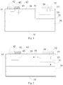
- Fig. 1 shows a cross sectional diagram of a lateral insulated gate bipolar transistor in an embodiment.
- the lateral insulated gate bipolar transistor includes a substrate 10, an anode terminal and a cathode terminal on the substrate 10, a drift region 30 and a gate 62 located between the anode terminal and the cathode terminal.
- the anode terminal includes an N-type buffer region 51 on the substrate; a P well 53 in the N-type buffer region 51; an N-region 55 located in the P well 53; two P+ shallow junctions 57 located on a surface of the P well 53; and an N+ shallow junction 59 located between the two P+ shallow junctions 57.
- the cathode terminal includes a P+ region 41 located on the substrate 10; a P-type body region 43 located between the P+ region 41 and the anode terminal; an N+ region 45 located at a surface of the P-type body region 43; and a cathode metal 42 as an electrode of the emitter.
- the gate 62 includes a gate oxide layer (not shown) and a polysilicon gate on the gate oxide layer.
- the gate 62 when the gate 62 is biased forwardly, the device channel is opened, the electronic current passes through the channel of the P-type body region 43 via the N+ region 45 of the emitter, and flows into the drift region 30 and the N-type buffer region 51 in sequence.
- the P+ shallow junctions 57 of the anode terminal when the P+ shallow junctions 57 of the anode terminal is biased forwardly and the bias voltage is lower, holes begin to inject into the N-type buffer region 51 downward from the P+ shallow junctions 57 and the P well 53 of the anode terminal; as the bias voltage on the anode metal 52 raises, the P+ shallow junctions 57 also inject holes into the drift region 30 laterally via the N-type buffer region 51, which achieves efficient majority carrier holes injection of multiple paths and significantly reduces the on-resistance.
- the anode When the lateral insulated gate bipolar transistor is turned off, the anode is biased inversely, a lower resistance path of electronic injection is formed by the N+ shallow junction 59, the N-region 55 and the N-type buffer region 51, and then residual minority carrier holes in the drift region 30 are extracted quickly to achieve a quick tuning-off, which ensures a quicker switching speed.
- the doped concentration of each region satisfies the following relationships: a doped concentration of the N-type buffer region 51 is less than a doped concentration of the P well 53; the doped concentration of the P well 53 is slightly less than a doped concentration of the N-region 55; and the doped concentration of the N-region 55 is less than doped concentrations of the two P+ shallow junctions 57 and the N+ shallow junction 59.
- the N-region 55 is a key of controlling lifetime of minority carrier and is designed to have a suitable doped concentration, which can form a longitudinal (the P+ shallow junctions 57 ⁇ the N-region 55 ⁇ the P well 53) VPNP.
- FIG. 2 illustrates the flow direction of holes when the anode is biased forwardly by an arrow.
- the one of two P+ shallow junctions 57 that is positioned closer to the cathode terminal and the N+ shallow junction 59 are disposed at a surface of the N-region 55.
- the doped concentration of the N-type buffer region 51 is 10 15 /cm3; the doped concentration of the P well 53 is 10 17 /cm 3 ; and the doped concentrations of the P+ shallow junctions 57 and the N+ shallow junction 59 are 10 20 /cm 3 .
- the anode terminal forms a deep and light N-type buffer region 51 firstly by injecting N-type ions and experiencing a drive-in process under a high temperature and for a long time, and minority carriers can be captured when the lateral insulated gate bipolar transistor is turned off.
- P-type ions are injected into the N-type buffer region 51 and the P well 53 is formed by thermal annealing; a N-region 55 of a longitudinal junction depth with a certain depth by injecting N-type ions and annealing; the N-region 55 serves as a channel of a certain width for injecting electrons and extracting holes, and then the P+ shallow junctions 57 and the N+ shallow junction 59 are formed by performing the injection process.
- SOI LIGBT devices widely apply in the automotive electronics, home electronics and communications and industrial applications due to a lower current leakage, a lower on-state resistance, a high input impedance, a high package density, a fast switching, a significant noise reduction effect and a working feasibility under high temperature caused by the trench isolation.
- the LIGBT shown in Fig. 1 is an silicon on insulator type lateral insulated gate bipolar transistor (SOI-LIGBT) includes a buried oxide layer 20 located between the substrate 10 and the draft region 30, wherein the substrate 10 is a P-type substrate, and the drift region 30 is an N-type drift region.
- the junction depth of the P+ region 41 is deeper and extends to the buried oxide layer 20.
Landscapes
- Insulated Gate Type Field-Effect Transistor (AREA)
- Thin Film Transistor (AREA)
- Bipolar Transistors (AREA)
- Thyristors (AREA)
Abstract
Description
- The present invention relates to a semiconductor process, and particularly relates to a lateral insulated gate bipolar transistor.
- Lateral Insulated-Gate Bipolar Transistor (LIGBT) is commonly used in the output stage of a high-voltage power-driven integrated circuit, and the structure of LIGBT causes a lower on-resistance due to a conductive modulation effect formed by injection of double carriers electrons and holes, compared with reducing of the on-resistance by a single carrier of a lateral double diffusion metal-oxide semiconductor field effect transistor (LDMOS).
- However, when LIGBT is turned off, the drift region of LIGBT has a longer turning-off time due to residual minority carrier holes, so there is a problem of a larger power consumption. Because the on-resistance and the turning-off time are inversely proportional to the hole concentration, how to obtain a balance between the on-resistance and the turning-off time becomes a continual improvement in the LIGBT device.
- Accordingly, it is necessary to provide a lateral insulated gate bipolar transistor, which can be turned off quickly while ensuring a lower on-resistance.
- A lateral insulated gate bipolar transistor includes: a substrate; an anode terminal located on the substrate including: an N-type buffer region on the substrate; a P well in the N-type buffer region; an N-region located in the P well; two P+ shallow junctions located on a surface of the P well; and an N+ shallow junction located between the two P+ shallow junctions; a cathode terminal located on the substrate; a draft region between the anode terminal and cathode terminal; and a gate between the anode terminal and cathode terminal.
- When the above lateral insulated gate bipolar transistor is turned on forwardly, an efficient injection of holes can be achieved and the on-resistance can be reduced by a longitudinal injection of the P+ shallow junctions and the P well and a lateral injection of the P+ shallow junctions; when the above lateral insulated gate bipolar transistor is turned off inversely, a path quickly extracting minority carrier (holes) is formed by the N-type buffer region, the N-region and the N+ shallow junctions, which achieves a quick turning-off and reduces a turning-off state loss.
- To illustrate the technical solutions according to the embodiments of the present invention or in the prior art more clearly, the accompanying drawings for describing the embodiments or the prior art are introduced briefly in the following. Apparently, the accompanying drawings in the following description are only some embodiments of the present invention, and persons of ordinary skill in the art can derive other drawings from the accompanying drawings without creative efforts.
-
Fig. 1 shows a cross sectional diagram of a lateral insulated gate bipolar transistor in an embodiment; -
Fig. 2 shows a flow direction diagram of holes when the anode of the device shown inFig. 1 is biased forwardly. - Embodiments of the invention are described more fully hereinafter with reference to the accompanying drawings. The various embodiments of the invention may, however, be embodied in many different forms and should not be construed as limited to the embodiments set forth herein. Rather, these embodiments are provided so that this disclosure will be thorough and complete, and will fully convey the scope of the invention to those skilled in the art. Elements that are identified using the same or similar reference characters refer to the same or similar elements.
- The terminology used herein is for the purpose of describing particular embodiments only and is not intended to be limiting of the invention. As used herein, the singular forms "a", "an" and "the" are intended to include the plural forms as well, unless the context clearly indicates otherwise. It will be further understood that the terms "comprises" and/or "comprising," when used in this specification, specify the presence of stated features, integers, steps, operations, elements, and/or components, but do not preclude the presence or addition of one or more other features, integers, steps, operations, elements, components, and/or groups thereof.
- It will be understood that when an element is referred to as being "connected" or "coupled" to another element, it can be directly connected or coupled to the other element or intervening elements may be present. In contrast, if an element is referred to as being "directly connected" or "directly coupled" to another element, there are no intervening elements present.
- It will be understood that, although the terms first, second, etc. may be used herein to describe various elements, these elements should not be limited by these terms. These terms are only used to distinguish one element from another. Thus, a first element could be termed a second element without departing from the teachings of the present invention.
- Unless otherwise defined, all terms (including technical and scientific terms) used herein have the same meaning as commonly understood by one of ordinary skill in the art to which this invention belongs. It will be further understood that terms, such as those defined in commonly used dictionaries, should be interpreted as having a meaning that is consistent with their meaning in the context of the relevant art and will not be interpreted in an idealized or overly formal sense unless expressly so defined herein.
-
Fig. 1 shows a cross sectional diagram of a lateral insulated gate bipolar transistor in an embodiment. The lateral insulated gate bipolar transistor includes asubstrate 10, an anode terminal and a cathode terminal on thesubstrate 10, adrift region 30 and agate 62 located between the anode terminal and the cathode terminal. The anode terminal includes an N-type buffer region 51 on the substrate; aP well 53 in the N-type buffer region 51; an N-region 55 located in theP well 53; two P+shallow junctions 57 located on a surface of theP well 53; and an N+shallow junction 59 located between the two P+shallow junctions 57. The cathode terminal includes aP+ region 41 located on thesubstrate 10; a P-type body region 43 located between theP+ region 41 and the anode terminal; anN+ region 45 located at a surface of the P-type body region 43; and acathode metal 42 as an electrode of the emitter. Thegate 62 includes a gate oxide layer (not shown) and a polysilicon gate on the gate oxide layer. - For the above lateral insulated gate bipolar transistor, when the
gate 62 is biased forwardly, the device channel is opened, the electronic current passes through the channel of the P-type body region 43 via theN+ region 45 of the emitter, and flows into thedrift region 30 and the N-type buffer region 51 in sequence. However, when the P+shallow junctions 57 of the anode terminal is biased forwardly and the bias voltage is lower, holes begin to inject into the N-type buffer region 51 downward from the P+shallow junctions 57 and theP well 53 of the anode terminal; as the bias voltage on theanode metal 52 raises, the P+shallow junctions 57 also inject holes into thedrift region 30 laterally via the N-type buffer region 51, which achieves efficient majority carrier holes injection of multiple paths and significantly reduces the on-resistance. When the lateral insulated gate bipolar transistor is turned off, the anode is biased inversely, a lower resistance path of electronic injection is formed by the N+shallow junction 59, the N-region 55 and the N-type buffer region 51, and then residual minority carrier holes in thedrift region 30 are extracted quickly to achieve a quick tuning-off, which ensures a quicker switching speed. Therefore, when the device is turned on forwardly, an efficient injection of holes can be achieved and the on-resistance can be reduced by a longitudinal injection of the P+shallow junctions 57 and theP well 53 and a lateral injection of the P+shallow junctions 57; when the device is turned off inversely, a path quickly extracting minority carrier (holes) is formed by the N-type buffer region 51, the N-region 55 and the N+shallow junctions 59, which achieves a quick turning-off and reduces a turning-off state loss. - In the embodiment shown in
Fig. 1 , the doped concentration of each region satisfies the following relationships: a doped concentration of the N-type buffer region 51 is less than a doped concentration of theP well 53; the doped concentration of theP well 53 is slightly less than a doped concentration of the N-region 55; and the doped concentration of the N-region 55 is less than doped concentrations of the two P+shallow junctions 57 and the N+shallow junction 59. The N-region 55 is a key of controlling lifetime of minority carrier and is designed to have a suitable doped concentration, which can form a longitudinal (the P+shallow junctions 57→the N-region 55→the P well 53) VPNP.Fig. 2 illustrates the flow direction of holes when the anode is biased forwardly by an arrow. In order to obtain an idea flow path of carriers, in the embodiment shown inFig. 1 and Fig. 2 , the one of two P+shallow junctions 57 that is positioned closer to the cathode terminal and the N+shallow junction 59 are disposed at a surface of the N-region 55. - In an embodiment, the doped concentration of the N-
type buffer region 51 is 1015/cm3; the doped concentration of theP well 53 is 1017/cm3; and the doped concentrations of the P+shallow junctions 57 and the N+shallow junction 59 are 1020/cm3. - When the lateral insulated gate bipolar transistor is manufactured, the anode terminal forms a deep and light N-
type buffer region 51 firstly by injecting N-type ions and experiencing a drive-in process under a high temperature and for a long time, and minority carriers can be captured when the lateral insulated gate bipolar transistor is turned off. Then, P-type ions are injected into the N-type buffer region 51 and theP well 53 is formed by thermal annealing; a N-region 55 of a longitudinal junction depth with a certain depth by injecting N-type ions and annealing; the N-region 55 serves as a channel of a certain width for injecting electrons and extracting holes, and then the P+shallow junctions 57 and the N+shallow junction 59 are formed by performing the injection process. - The silicon on insulator (SOI) technology is increasingly important in HVIC and SPIC applications, while a lower on-resistance characteristic of IGBT devices caused by high input impedance and conductive modulation effect increasingly plays an important role in power device applications. Compared with the bulk silicon junction isolation device, SOI LIGBT devices widely apply in the automotive electronics, home electronics and communications and industrial applications due to a lower current leakage, a lower on-state resistance, a high input impedance, a high package density, a fast switching, a significant noise reduction effect and a working feasibility under high temperature caused by the trench isolation. It is particularly important to require an efficient injection of holes and a significant conductive modulation effect to reduce the on-state resistance, but respectively increase the turning-off loss caused by that minority carrier holes cannot be annihilated quickly when the device is turned off. The LIGBT shown in
Fig. 1 is an silicon on insulator type lateral insulated gate bipolar transistor (SOI-LIGBT) includes a buriedoxide layer 20 located between thesubstrate 10 and thedraft region 30, wherein thesubstrate 10 is a P-type substrate, and thedrift region 30 is an N-type drift region. The junction depth of theP+ region 41 is deeper and extends to the buriedoxide layer 20. - Although the invention is illustrated and described herein with reference to specific embodiments, the invention is not intended to be limited to the details shown. Rather, various modifications may be made in the details within the scope and range of equivalents of the claims and without departing from the invention.
Claims (10)
- A lateral insulated gate bipolar transistor, comprising:a substrate;an anode terminal located on the substrate, comprising:an N-type buffer region located on the substrate;a P well located in the N-type buffer region;an N-region located in the P well;two P+ shallow junctions located on a surface of the P well; andan N+ shallow junction located between the two P+ shallow junctions;a cathode terminal located on the substrate;a draft region between the anode terminal and cathode terminal; anda gate between the anode terminal and cathode terminal.
- The lateral insulated gate bipolar transistor of claim 1, characterized in that, a doped concentration of the N-type buffer region is less than a doped concentration of the P well; the doped concentration of the P well is less than a doped concentration of the N-region; and the doped concentration of the N-region is less than doped concentrations of the two P+ shallow junctions and the N+ shallow junction.
- The lateral insulated gate bipolar transistor of claim 2, characterized in that, the doped concentration of the N-type buffer region is from 1*1015/cm3 to 1*1016/cm3; the doped concentration of the P well is from 1*1017/cm3 to 1*1018/cm3; and the doped concentrations of the two P+ shallow junctions and the N+ shallow junction are from 1*1020/cm3 to 1*1021/cm3.
- The lateral insulated gate bipolar transistor of claim 3, characterized in that, the doped concentration of the N-type buffer region is 5*1015/cm3; and the doped concentration of the P well is 8*1017/cm3.
- The lateral insulated gate bipolar transistor of claim 1, characterized in that, the lateral insulated gate bipolar transistor is a silicon-on-insulator type lateral insulated gate bipolar transistor, and the lateral insulated gate bipolar transistor further comprises a buried oxide layer located between the substrate and the draft region.
- The lateral insulated gate bipolar transistor of claim 1, characterized in that, the substrate is a P-type substrate; and the draft region is an N-type draft region.
- The lateral insulated gate bipolar transistor of claim 6, characterized in that, the cathode terminal comprises:a P+ region located on the substrate;a P-type body region located between the P+ region and the anode terminal; andan N+ region located at a surface of the P-type body region.
- The lateral insulated gate bipolar transistor of claim 7, characterized in that, the P+ region extends to the buried oxide layer.
- The lateral insulated gate bipolar transistor of claim 7, characterized in that, the anode terminal further comprises an anode metal; the cathode terminal further comprises a cathode metal; and the gate comprises a gate oxide layer and a polysilicon gate on the gate oxide layer.
- The lateral insulated gate bipolar transistor of claim 1, characterized in that, one of two P+ shallow junctions that is positioned closer to the cathode terminal and the N+ shallow junction are disposed at a surface of the N-region.
Applications Claiming Priority (2)
| Application Number | Priority Date | Filing Date | Title |
|---|---|---|---|
| CN201410810523.2A CN105789286B (en) | 2014-12-22 | 2014-12-22 | Landscape insulation bar double-pole-type transistor |
| PCT/CN2015/089302 WO2016101654A1 (en) | 2014-12-22 | 2015-09-10 | Lateral insulated-gate bipolar transistor |
Publications (3)
| Publication Number | Publication Date |
|---|---|
| EP3240039A1 true EP3240039A1 (en) | 2017-11-01 |
| EP3240039A4 EP3240039A4 (en) | 2018-08-01 |
| EP3240039B1 EP3240039B1 (en) | 2021-07-28 |
Family
ID=56149178
Family Applications (1)
| Application Number | Title | Priority Date | Filing Date |
|---|---|---|---|
| EP15871728.0A Active EP3240039B1 (en) | 2014-12-22 | 2015-09-10 | Lateral insulated-gate bipolar transistor |
Country Status (5)
| Country | Link |
|---|---|
| US (1) | US9905680B2 (en) |
| EP (1) | EP3240039B1 (en) |
| JP (1) | JP6430650B2 (en) |
| CN (1) | CN105789286B (en) |
| WO (1) | WO2016101654A1 (en) |
Families Citing this family (2)
| Publication number | Priority date | Publication date | Assignee | Title |
|---|---|---|---|---|
| CN110010678A (en) * | 2018-01-04 | 2019-07-12 | 中兴通讯股份有限公司 | Lateral insulated gate bipolar transistor and preparation method thereof |
| CN114937666B (en) * | 2022-05-12 | 2025-03-25 | 重庆邮电大学 | An RC-LIGBT device with integrated dual self-biased MOS and low turn-off loss |
Family Cites Families (15)
| Publication number | Priority date | Publication date | Assignee | Title |
|---|---|---|---|---|
| US5396087A (en) * | 1992-12-14 | 1995-03-07 | North Carolina State University | Insulated gate bipolar transistor with reduced susceptibility to parasitic latch-up |
| JP3085037B2 (en) * | 1993-08-18 | 2000-09-04 | 富士電機株式会社 | Insulated gate bipolar transistor |
| GB2289371B (en) * | 1994-05-05 | 1997-11-19 | Fuji Electric Co Ltd | A semiconductor device and control method |
| US5665988A (en) * | 1995-02-09 | 1997-09-09 | Fuji Electric Co., Ltd. | Conductivity-modulation semiconductor |
| WO1996036076A1 (en) * | 1995-05-11 | 1996-11-14 | Fuji Electric Co., Ltd. | Emitter switched thyristor |
| US5731603A (en) * | 1995-08-24 | 1998-03-24 | Kabushiki Kaisha Toshiba | Lateral IGBT |
| JP3367839B2 (en) * | 1995-09-18 | 2003-01-20 | 株式会社東芝 | Semiconductor device |
| US7465964B2 (en) * | 2005-12-30 | 2008-12-16 | Cambridge Semiconductor Limited | Semiconductor device in which an injector region is isolated from a substrate |
| CN2914330Y (en) | 2006-05-24 | 2007-06-20 | 杭州电子科技大学 | Anti-ESD integrated SOI LIGBT unit |
| US7605446B2 (en) * | 2006-07-14 | 2009-10-20 | Cambridge Semiconductor Limited | Bipolar high voltage/power semiconductor device having first and second insulated gated and method of operation |
| US8482031B2 (en) * | 2009-09-09 | 2013-07-09 | Cambridge Semiconductor Limited | Lateral insulated gate bipolar transistors (LIGBTS) |
| CN102290436B (en) * | 2011-09-15 | 2016-08-03 | 江苏宏微科技有限公司 | Novel structure for back side of IGBT and preparation method thereof |
| CN102832213B (en) * | 2012-08-31 | 2014-10-29 | 电子科技大学 | Lateral insulator gate bipolar transistor (LIGBT) device with electronic static discharge (ESD) protection function |
| US9070735B2 (en) * | 2013-07-02 | 2015-06-30 | Cambridge Microelectronics Ltd. | Lateral power semiconductor transistors |
| CN103413824B (en) * | 2013-07-17 | 2015-12-23 | 电子科技大学 | A kind of RC-LIGBT device and preparation method thereof |
-
2014
- 2014-12-22 CN CN201410810523.2A patent/CN105789286B/en active Active
-
2015
- 2015-09-10 US US15/538,450 patent/US9905680B2/en active Active
- 2015-09-10 EP EP15871728.0A patent/EP3240039B1/en active Active
- 2015-09-10 WO PCT/CN2015/089302 patent/WO2016101654A1/en not_active Ceased
- 2015-09-10 JP JP2017533840A patent/JP6430650B2/en active Active
Also Published As
| Publication number | Publication date |
|---|---|
| JP2018506179A (en) | 2018-03-01 |
| CN105789286B (en) | 2018-11-27 |
| WO2016101654A1 (en) | 2016-06-30 |
| EP3240039A4 (en) | 2018-08-01 |
| US20170352749A1 (en) | 2017-12-07 |
| US9905680B2 (en) | 2018-02-27 |
| EP3240039B1 (en) | 2021-07-28 |
| CN105789286A (en) | 2016-07-20 |
| JP6430650B2 (en) | 2018-11-28 |
Similar Documents
| Publication | Publication Date | Title |
|---|---|---|
| US9240469B2 (en) | Transverse ultra-thin insulated gate bipolar transistor having high current density | |
| US10084073B2 (en) | Lateral insulated-gate bipolar transistor and manufacturing method therefor | |
| CN105409004A (en) | Lateral power semiconductor transistors | |
| CN103579351A (en) | LDMOS (laterally diffused metal oxide semiconductor) device provided with super-junction buried layer | |
| KR102158345B1 (en) | Side insulated gate bipolar transistor and manufacturing method thereof | |
| CN115117162B (en) | Semiconductor devices and semiconductor circuits | |
| CN104518017A (en) | IGBT with reduced feedback capacitance | |
| CN106409915A (en) | Vertical double-diffusion metal oxide semiconductor field effect transistor | |
| CN105489644B (en) | IGBT device and preparation method thereof | |
| US9263560B2 (en) | Power semiconductor device having reduced gate-collector capacitance | |
| CN102832213B (en) | Lateral insulator gate bipolar transistor (LIGBT) device with electronic static discharge (ESD) protection function | |
| CN101656269A (en) | Trench DMOS device with low on-resistance | |
| EP3240039B1 (en) | Lateral insulated-gate bipolar transistor | |
| CN109920840B (en) | L-shaped SiO2Composite RC-LIGBT device with isolation layer | |
| CN109065626B (en) | Groove gate DMOS device with dielectric barrier layer | |
| CN109888006B (en) | A low-power silicon-on-insulator lateral insulated gate bipolar transistor | |
| CN106711189A (en) | A superjunction device | |
| CN115458593A (en) | A low-power LIGBT device with integrated self-biased PMOS | |
| US7910995B2 (en) | Structure and method for semiconductor power devices | |
| CN106298901A (en) | A kind of landscape insulation bar double-pole-type transistor of high hot carrier reliability | |
| CN106920840A (en) | The method for eliminating landscape insulation bar double-pole-type transistor tail currents | |
| CN104518008B (en) | A kind of technotron | |
| CN106384747A (en) | Field effect transistor | |
| CN102184958A (en) | Vertical double-diffusion MOS (Metal-Oxide Semiconductor) tube and manufacturing method thereof | |
| CN111129131A (en) | Planar Gate IGBT Devices |
Legal Events
| Date | Code | Title | Description |
|---|---|---|---|
| STAA | Information on the status of an ep patent application or granted ep patent |
Free format text: STATUS: THE INTERNATIONAL PUBLICATION HAS BEEN MADE |
|
| PUAI | Public reference made under article 153(3) epc to a published international application that has entered the european phase |
Free format text: ORIGINAL CODE: 0009012 |
|
| STAA | Information on the status of an ep patent application or granted ep patent |
Free format text: STATUS: REQUEST FOR EXAMINATION WAS MADE |
|
| 17P | Request for examination filed |
Effective date: 20170721 |
|
| AK | Designated contracting states |
Kind code of ref document: A1 Designated state(s): AL AT BE BG CH CY CZ DE DK EE ES FI FR GB GR HR HU IE IS IT LI LT LU LV MC MK MT NL NO PL PT RO RS SE SI SK SM TR |
|
| AX | Request for extension of the european patent |
Extension state: BA ME |
|
| DAV | Request for validation of the european patent (deleted) | ||
| DAX | Request for extension of the european patent (deleted) | ||
| A4 | Supplementary search report drawn up and despatched |
Effective date: 20180704 |
|
| RIC1 | Information provided on ipc code assigned before grant |
Ipc: H01L 29/06 20060101ALI20180628BHEP Ipc: H01L 29/08 20060101ALI20180628BHEP Ipc: H01L 29/739 20060101AFI20180628BHEP |
|
| STAA | Information on the status of an ep patent application or granted ep patent |
Free format text: STATUS: EXAMINATION IS IN PROGRESS |
|
| 17Q | First examination report despatched |
Effective date: 20201204 |
|
| GRAP | Despatch of communication of intention to grant a patent |
Free format text: ORIGINAL CODE: EPIDOSNIGR1 |
|
| STAA | Information on the status of an ep patent application or granted ep patent |
Free format text: STATUS: GRANT OF PATENT IS INTENDED |
|
| INTG | Intention to grant announced |
Effective date: 20210322 |
|
| RAP1 | Party data changed (applicant data changed or rights of an application transferred) |
Owner name: CSMC TECHNOLOGIES FAB2 CO., LTD. |
|
| GRAS | Grant fee paid |
Free format text: ORIGINAL CODE: EPIDOSNIGR3 |
|
| GRAA | (expected) grant |
Free format text: ORIGINAL CODE: 0009210 |
|
| STAA | Information on the status of an ep patent application or granted ep patent |
Free format text: STATUS: THE PATENT HAS BEEN GRANTED |
|
| AK | Designated contracting states |
Kind code of ref document: B1 Designated state(s): AL AT BE BG CH CY CZ DE DK EE ES FI FR GB GR HR HU IE IS IT LI LT LU LV MC MK MT NL NO PL PT RO RS SE SI SK SM TR |
|
| REG | Reference to a national code |
Ref country code: GB Ref legal event code: FG4D |
|
| REG | Reference to a national code |
Ref country code: CH Ref legal event code: EP |
|
| REG | Reference to a national code |
Ref country code: AT Ref legal event code: REF Ref document number: 1415492 Country of ref document: AT Kind code of ref document: T Effective date: 20210815 |
|
| REG | Reference to a national code |
Ref country code: IE Ref legal event code: FG4D |
|
| REG | Reference to a national code |
Ref country code: DE Ref legal event code: R096 Ref document number: 602015071800 Country of ref document: DE |
|
| REG | Reference to a national code |
Ref country code: LT Ref legal event code: MG9D |
|
| REG | Reference to a national code |
Ref country code: NL Ref legal event code: MP Effective date: 20210728 |
|
| REG | Reference to a national code |
Ref country code: AT Ref legal event code: MK05 Ref document number: 1415492 Country of ref document: AT Kind code of ref document: T Effective date: 20210728 |
|
| PG25 | Lapsed in a contracting state [announced via postgrant information from national office to epo] |
Ref country code: HR Free format text: LAPSE BECAUSE OF FAILURE TO SUBMIT A TRANSLATION OF THE DESCRIPTION OR TO PAY THE FEE WITHIN THE PRESCRIBED TIME-LIMIT Effective date: 20210728 Ref country code: RS Free format text: LAPSE BECAUSE OF FAILURE TO SUBMIT A TRANSLATION OF THE DESCRIPTION OR TO PAY THE FEE WITHIN THE PRESCRIBED TIME-LIMIT Effective date: 20210728 Ref country code: SE Free format text: LAPSE BECAUSE OF FAILURE TO SUBMIT A TRANSLATION OF THE DESCRIPTION OR TO PAY THE FEE WITHIN THE PRESCRIBED TIME-LIMIT Effective date: 20210728 Ref country code: AT Free format text: LAPSE BECAUSE OF FAILURE TO SUBMIT A TRANSLATION OF THE DESCRIPTION OR TO PAY THE FEE WITHIN THE PRESCRIBED TIME-LIMIT Effective date: 20210728 Ref country code: BG Free format text: LAPSE BECAUSE OF FAILURE TO SUBMIT A TRANSLATION OF THE DESCRIPTION OR TO PAY THE FEE WITHIN THE PRESCRIBED TIME-LIMIT Effective date: 20211028 Ref country code: LT Free format text: LAPSE BECAUSE OF FAILURE TO SUBMIT A TRANSLATION OF THE DESCRIPTION OR TO PAY THE FEE WITHIN THE PRESCRIBED TIME-LIMIT Effective date: 20210728 Ref country code: NO Free format text: LAPSE BECAUSE OF FAILURE TO SUBMIT A TRANSLATION OF THE DESCRIPTION OR TO PAY THE FEE WITHIN THE PRESCRIBED TIME-LIMIT Effective date: 20211028 Ref country code: NL Free format text: LAPSE BECAUSE OF FAILURE TO SUBMIT A TRANSLATION OF THE DESCRIPTION OR TO PAY THE FEE WITHIN THE PRESCRIBED TIME-LIMIT Effective date: 20210728 Ref country code: PT Free format text: LAPSE BECAUSE OF FAILURE TO SUBMIT A TRANSLATION OF THE DESCRIPTION OR TO PAY THE FEE WITHIN THE PRESCRIBED TIME-LIMIT Effective date: 20211129 Ref country code: ES Free format text: LAPSE BECAUSE OF FAILURE TO SUBMIT A TRANSLATION OF THE DESCRIPTION OR TO PAY THE FEE WITHIN THE PRESCRIBED TIME-LIMIT Effective date: 20210728 Ref country code: FI Free format text: LAPSE BECAUSE OF FAILURE TO SUBMIT A TRANSLATION OF THE DESCRIPTION OR TO PAY THE FEE WITHIN THE PRESCRIBED TIME-LIMIT Effective date: 20210728 |
|
| PG25 | Lapsed in a contracting state [announced via postgrant information from national office to epo] |
Ref country code: PL Free format text: LAPSE BECAUSE OF FAILURE TO SUBMIT A TRANSLATION OF THE DESCRIPTION OR TO PAY THE FEE WITHIN THE PRESCRIBED TIME-LIMIT Effective date: 20210728 Ref country code: LV Free format text: LAPSE BECAUSE OF FAILURE TO SUBMIT A TRANSLATION OF THE DESCRIPTION OR TO PAY THE FEE WITHIN THE PRESCRIBED TIME-LIMIT Effective date: 20210728 Ref country code: GR Free format text: LAPSE BECAUSE OF FAILURE TO SUBMIT A TRANSLATION OF THE DESCRIPTION OR TO PAY THE FEE WITHIN THE PRESCRIBED TIME-LIMIT Effective date: 20211029 |
|
| PG25 | Lapsed in a contracting state [announced via postgrant information from national office to epo] |
Ref country code: DK Free format text: LAPSE BECAUSE OF FAILURE TO SUBMIT A TRANSLATION OF THE DESCRIPTION OR TO PAY THE FEE WITHIN THE PRESCRIBED TIME-LIMIT Effective date: 20210728 |
|
| REG | Reference to a national code |
Ref country code: DE Ref legal event code: R097 Ref document number: 602015071800 Country of ref document: DE Ref country code: CH Ref legal event code: PL |
|
| REG | Reference to a national code |
Ref country code: BE Ref legal event code: MM Effective date: 20210930 |
|
| PG25 | Lapsed in a contracting state [announced via postgrant information from national office to epo] |
Ref country code: SM Free format text: LAPSE BECAUSE OF FAILURE TO SUBMIT A TRANSLATION OF THE DESCRIPTION OR TO PAY THE FEE WITHIN THE PRESCRIBED TIME-LIMIT Effective date: 20210728 Ref country code: SK Free format text: LAPSE BECAUSE OF FAILURE TO SUBMIT A TRANSLATION OF THE DESCRIPTION OR TO PAY THE FEE WITHIN THE PRESCRIBED TIME-LIMIT Effective date: 20210728 Ref country code: RO Free format text: LAPSE BECAUSE OF FAILURE TO SUBMIT A TRANSLATION OF THE DESCRIPTION OR TO PAY THE FEE WITHIN THE PRESCRIBED TIME-LIMIT Effective date: 20210728 Ref country code: MC Free format text: LAPSE BECAUSE OF FAILURE TO SUBMIT A TRANSLATION OF THE DESCRIPTION OR TO PAY THE FEE WITHIN THE PRESCRIBED TIME-LIMIT Effective date: 20210728 Ref country code: EE Free format text: LAPSE BECAUSE OF FAILURE TO SUBMIT A TRANSLATION OF THE DESCRIPTION OR TO PAY THE FEE WITHIN THE PRESCRIBED TIME-LIMIT Effective date: 20210728 Ref country code: CZ Free format text: LAPSE BECAUSE OF FAILURE TO SUBMIT A TRANSLATION OF THE DESCRIPTION OR TO PAY THE FEE WITHIN THE PRESCRIBED TIME-LIMIT Effective date: 20210728 Ref country code: AL Free format text: LAPSE BECAUSE OF FAILURE TO SUBMIT A TRANSLATION OF THE DESCRIPTION OR TO PAY THE FEE WITHIN THE PRESCRIBED TIME-LIMIT Effective date: 20210728 |
|
| PLBE | No opposition filed within time limit |
Free format text: ORIGINAL CODE: 0009261 |
|
| STAA | Information on the status of an ep patent application or granted ep patent |
Free format text: STATUS: NO OPPOSITION FILED WITHIN TIME LIMIT |
|
| 26N | No opposition filed |
Effective date: 20220429 |
|
| PG25 | Lapsed in a contracting state [announced via postgrant information from national office to epo] |
Ref country code: LU Free format text: LAPSE BECAUSE OF NON-PAYMENT OF DUE FEES Effective date: 20210910 Ref country code: IT Free format text: LAPSE BECAUSE OF FAILURE TO SUBMIT A TRANSLATION OF THE DESCRIPTION OR TO PAY THE FEE WITHIN THE PRESCRIBED TIME-LIMIT Effective date: 20210728 Ref country code: IE Free format text: LAPSE BECAUSE OF NON-PAYMENT OF DUE FEES Effective date: 20210910 Ref country code: BE Free format text: LAPSE BECAUSE OF NON-PAYMENT OF DUE FEES Effective date: 20210930 |
|
| PG25 | Lapsed in a contracting state [announced via postgrant information from national office to epo] |
Ref country code: LI Free format text: LAPSE BECAUSE OF NON-PAYMENT OF DUE FEES Effective date: 20210930 Ref country code: CH Free format text: LAPSE BECAUSE OF NON-PAYMENT OF DUE FEES Effective date: 20210930 |
|
| PG25 | Lapsed in a contracting state [announced via postgrant information from national office to epo] |
Ref country code: HU Free format text: LAPSE BECAUSE OF FAILURE TO SUBMIT A TRANSLATION OF THE DESCRIPTION OR TO PAY THE FEE WITHIN THE PRESCRIBED TIME-LIMIT; INVALID AB INITIO Effective date: 20150910 |
|
| PG25 | Lapsed in a contracting state [announced via postgrant information from national office to epo] |
Ref country code: CY Free format text: LAPSE BECAUSE OF FAILURE TO SUBMIT A TRANSLATION OF THE DESCRIPTION OR TO PAY THE FEE WITHIN THE PRESCRIBED TIME-LIMIT Effective date: 20210728 |
|
| PG25 | Lapsed in a contracting state [announced via postgrant information from national office to epo] |
Ref country code: MK Free format text: LAPSE BECAUSE OF FAILURE TO SUBMIT A TRANSLATION OF THE DESCRIPTION OR TO PAY THE FEE WITHIN THE PRESCRIBED TIME-LIMIT Effective date: 20210728 |
|
| PG25 | Lapsed in a contracting state [announced via postgrant information from national office to epo] |
Ref country code: MT Free format text: LAPSE BECAUSE OF FAILURE TO SUBMIT A TRANSLATION OF THE DESCRIPTION OR TO PAY THE FEE WITHIN THE PRESCRIBED TIME-LIMIT Effective date: 20210728 |
|
| REG | Reference to a national code |
Ref country code: DE Ref legal event code: R079 Ref document number: 602015071800 Country of ref document: DE Free format text: PREVIOUS MAIN CLASS: H01L0029739000 Ipc: H10D0012000000 |
|
| PGFP | Annual fee paid to national office [announced via postgrant information from national office to epo] |
Ref country code: DE Payment date: 20250919 Year of fee payment: 11 |
|
| PGFP | Annual fee paid to national office [announced via postgrant information from national office to epo] |
Ref country code: GB Payment date: 20250919 Year of fee payment: 11 |
|
| PGFP | Annual fee paid to national office [announced via postgrant information from national office to epo] |
Ref country code: FR Payment date: 20250922 Year of fee payment: 11 |
|
| PG25 | Lapsed in a contracting state [announced via postgrant information from national office to epo] |
Ref country code: TR Free format text: LAPSE BECAUSE OF FAILURE TO SUBMIT A TRANSLATION OF THE DESCRIPTION OR TO PAY THE FEE WITHIN THE PRESCRIBED TIME-LIMIT Effective date: 20210728 |