EP3240009A1 - Photoelectric surface, photoelectric conversion tube, image intensifier, and photomultiplier tube - Google Patents
Photoelectric surface, photoelectric conversion tube, image intensifier, and photomultiplier tube Download PDFInfo
- Publication number
- EP3240009A1 EP3240009A1 EP15872812.1A EP15872812A EP3240009A1 EP 3240009 A1 EP3240009 A1 EP 3240009A1 EP 15872812 A EP15872812 A EP 15872812A EP 3240009 A1 EP3240009 A1 EP 3240009A1
- Authority
- EP
- European Patent Office
- Prior art keywords
- film
- photoelectric
- photoelectric surface
- photoelectric conversion
- quantum efficiency
- Prior art date
- Legal status (The legal status is an assumption and is not a legal conclusion. Google has not performed a legal analysis and makes no representation as to the accuracy of the status listed.)
- Granted
Links
Images




Classifications
-
- H—ELECTRICITY
- H01—ELECTRIC ELEMENTS
- H01J—ELECTRIC DISCHARGE TUBES OR DISCHARGE LAMPS
- H01J1/00—Details of electrodes, of magnetic control means, of screens, or of the mounting or spacing thereof, common to two or more basic types of discharge tubes or lamps
- H01J1/02—Main electrodes
- H01J1/34—Photo-emissive cathodes
-
- H—ELECTRICITY
- H01—ELECTRIC ELEMENTS
- H01J—ELECTRIC DISCHARGE TUBES OR DISCHARGE LAMPS
- H01J1/00—Details of electrodes, of magnetic control means, of screens, or of the mounting or spacing thereof, common to two or more basic types of discharge tubes or lamps
- H01J1/54—Screens on or from which an image or pattern is formed, picked-up, converted, or stored; Luminescent coatings on vessels
- H01J1/78—Photoelectric screens; Charge-storage screens
-
- H—ELECTRICITY
- H01—ELECTRIC ELEMENTS
- H01J—ELECTRIC DISCHARGE TUBES OR DISCHARGE LAMPS
- H01J29/00—Details of cathode-ray tubes or of electron-beam tubes of the types covered by group H01J31/00
- H01J29/02—Electrodes; Screens; Mounting, supporting, spacing or insulating thereof
- H01J29/10—Screens on or from which an image or pattern is formed, picked up, converted or stored
- H01J29/36—Photoelectric screens; Charge-storage screens
- H01J29/38—Photoelectric screens; Charge-storage screens not using charge storage, e.g. photo-emissive screen, extended cathode
-
- H—ELECTRICITY
- H01—ELECTRIC ELEMENTS
- H01J—ELECTRIC DISCHARGE TUBES OR DISCHARGE LAMPS
- H01J31/00—Cathode ray tubes; Electron beam tubes
- H01J31/08—Cathode ray tubes; Electron beam tubes having a screen on or from which an image or pattern is formed, picked up, converted, or stored
- H01J31/50—Image-conversion or image-amplification tubes, i.e. having optical, X-ray, or analogous input, and optical output
-
- H—ELECTRICITY
- H01—ELECTRIC ELEMENTS
- H01J—ELECTRIC DISCHARGE TUBES OR DISCHARGE LAMPS
- H01J31/00—Cathode ray tubes; Electron beam tubes
- H01J31/08—Cathode ray tubes; Electron beam tubes having a screen on or from which an image or pattern is formed, picked up, converted, or stored
- H01J31/50—Image-conversion or image-amplification tubes, i.e. having optical, X-ray, or analogous input, and optical output
- H01J31/506—Image-conversion or image-amplification tubes, i.e. having optical, X-ray, or analogous input, and optical output tubes using secondary emission effect
-
- H—ELECTRICITY
- H01—ELECTRIC ELEMENTS
- H01J—ELECTRIC DISCHARGE TUBES OR DISCHARGE LAMPS
- H01J40/00—Photoelectric discharge tubes not involving the ionisation of a gas
- H01J40/02—Details
- H01J40/04—Electrodes
- H01J40/06—Photo-emissive cathodes
-
- H—ELECTRICITY
- H01—ELECTRIC ELEMENTS
- H01J—ELECTRIC DISCHARGE TUBES OR DISCHARGE LAMPS
- H01J40/00—Photoelectric discharge tubes not involving the ionisation of a gas
- H01J40/16—Photoelectric discharge tubes not involving the ionisation of a gas having photo- emissive cathode, e.g. alkaline photoelectric cell
-
- H—ELECTRICITY
- H10—SEMICONDUCTOR DEVICES; ELECTRIC SOLID-STATE DEVICES NOT OTHERWISE PROVIDED FOR
- H10F—INORGANIC SEMICONDUCTOR DEVICES SENSITIVE TO INFRARED RADIATION, LIGHT, ELECTROMAGNETIC RADIATION OF SHORTER WAVELENGTH OR CORPUSCULAR RADIATION
- H10F77/00—Constructional details of devices covered by this subclass
- H10F77/10—Semiconductor bodies
- H10F77/12—Active materials
- H10F77/121—Active materials comprising only selenium or only tellurium
-
- H—ELECTRICITY
- H10—SEMICONDUCTOR DEVICES; ELECTRIC SOLID-STATE DEVICES NOT OTHERWISE PROVIDED FOR
- H10F—INORGANIC SEMICONDUCTOR DEVICES SENSITIVE TO INFRARED RADIATION, LIGHT, ELECTROMAGNETIC RADIATION OF SHORTER WAVELENGTH OR CORPUSCULAR RADIATION
- H10F77/00—Constructional details of devices covered by this subclass
- H10F77/10—Semiconductor bodies
- H10F77/16—Material structures, e.g. crystalline structures, film structures or crystal plane orientations
- H10F77/169—Thin semiconductor films on metallic or insulating substrates
- H10F77/1696—Thin semiconductor films on metallic or insulating substrates the films including Group II-VI materials, e.g. CdTe or CdS
-
- H—ELECTRICITY
- H01—ELECTRIC ELEMENTS
- H01J—ELECTRIC DISCHARGE TUBES OR DISCHARGE LAMPS
- H01J2201/00—Electrodes common to discharge tubes
- H01J2201/34—Photoemissive electrodes
- H01J2201/342—Cathodes
- H01J2201/3421—Composition of the emitting surface
- H01J2201/3423—Semiconductors, e.g. GaAs, NEA emitters
-
- H—ELECTRICITY
- H01—ELECTRIC ELEMENTS
- H01J—ELECTRIC DISCHARGE TUBES OR DISCHARGE LAMPS
- H01J2201/00—Electrodes common to discharge tubes
- H01J2201/34—Photoemissive electrodes
- H01J2201/342—Cathodes
- H01J2201/3421—Composition of the emitting surface
- H01J2201/3426—Alkaline metal compounds, e.g. Na-K-Sb
-
- H—ELECTRICITY
- H01—ELECTRIC ELEMENTS
- H01J—ELECTRIC DISCHARGE TUBES OR DISCHARGE LAMPS
- H01J2231/00—Cathode ray tubes or electron beam tubes
- H01J2231/50—Imaging and conversion tubes
- H01J2231/50005—Imaging and conversion tubes characterised by form of illumination
- H01J2231/5001—Photons
- H01J2231/50015—Light
- H01J2231/50021—Ultraviolet
-
- H—ELECTRICITY
- H01—ELECTRIC ELEMENTS
- H01J—ELECTRIC DISCHARGE TUBES OR DISCHARGE LAMPS
- H01J31/00—Cathode ray tubes; Electron beam tubes
- H01J31/08—Cathode ray tubes; Electron beam tubes having a screen on or from which an image or pattern is formed, picked up, converted, or stored
- H01J31/49—Pick-up adapted for an input of electromagnetic radiation other than visible light and having an electric output, e.g. for an input of X-rays, for an input of infrared radiation
-
- Y—GENERAL TAGGING OF NEW TECHNOLOGICAL DEVELOPMENTS; GENERAL TAGGING OF CROSS-SECTIONAL TECHNOLOGIES SPANNING OVER SEVERAL SECTIONS OF THE IPC; TECHNICAL SUBJECTS COVERED BY FORMER USPC CROSS-REFERENCE ART COLLECTIONS [XRACs] AND DIGESTS
- Y02—TECHNOLOGIES OR APPLICATIONS FOR MITIGATION OR ADAPTATION AGAINST CLIMATE CHANGE
- Y02E—REDUCTION OF GREENHOUSE GAS [GHG] EMISSIONS, RELATED TO ENERGY GENERATION, TRANSMISSION OR DISTRIBUTION
- Y02E10/00—Energy generation through renewable energy sources
- Y02E10/50—Photovoltaic [PV] energy
Definitions
- the present invention relates to a photoelectric surface, a photoelectric conversion tube having the photoelectric surface, an image intensifier, and a photomultiplier tube.
- Patent Literatures 1, 2 and 3 disclose photoelectric surfaces having a laminated structure.
- the photoelectric surface disclosed in Patent Literature 1 has a laminated structure in which a substrate, a base film, an intermediate film, and a photoelectric conversion film are laminated in this order.
- the photoelectric surfaces disclosed in Patent Literatures 2 and 3 each have a laminated structure in which a window material, a base film, and a photoelectron emitting film are laminated in this order.
- Patent Literatures 1, 2 and 3 are used for detection of flames.
- a flame has a particular spectrum in a wavelength range of 300 nm or less.
- the sunlight reached the ground has a very narrow spectrum in an ultraviolet band of 300 nm or less due to absorption of an ozone layer.
- the band in which the spectrum of the sunlight becomes very narrow is also referred to as a solar blind band.
- the solar blind band as long as the photoelectric surface exhibits good sensitivity, it is possible to expect good light detection properties in which the effect of the sunlight is suppressed.
- a photoelectric surface having a laminated structure including: a window material that transmits ultraviolet rays, a conductive film that is formed on the window material and has conductivity, an intermediate film that is formed on the conductive film and includes a compound of magnesium and fluorine, and a photoelectric conversion film that is formed on the intermediate film and includes tellurium and an alkali metal.
- the photoelectric conversion film of the photoelectric surface includes tellurium and an alkali metal, a wavelength band detected by the photoelectric surface can be set to an ultraviolet band including a solar blind band.
- the intermediate film including a compound of magnesium and fluorine is formed between the photoelectric conversion film and the conductive film. Since the intermediate film including a compound of magnesium and fluorine has a relatively large band gap, a film having a large band gap is disposed on the surface of the photoelectric conversion film on the side of the window material. Then, the curvature of the band occurs and the photoelectron extraction efficiency is improved.
- the photoelectric surface it is possible to improve the sensitivity in an ultraviolet band.
- the compound may be magnesium fluoride and the alkali metal may be cesium. According to the constitutions thereof, since lattice mismatch generated between the photoelectric conversion film and the intermediate film is likely to be suppressed, it is possible to suppress a decrease in the crystallinity of the photoelectric conversion film. Accordingly, it is possible to further improve the sensitivity.
- the conductive film may include titanium. According to the constitution, the photoelectrons generated in the photoelectric conversion film can be efficiently extracted.
- the window material may include quartz. According to the constitution, since the attenuation of light occurring when the light passes through the window material is suppressed, it is possible to further improve the sensitivity.
- a photoelectric conversion tube including: a vacuum container that includes the photoelectric surface. Since the photoelectric conversion tube includes the photoelectric surface, it is possible to improve the sensitivity in an ultraviolet band.
- an image intensifier including: a vacuum container that includes the photoelectric surface, electron multiplier means that is accommodated in the vacuum container and multiplies electrons emitted from the photoelectric conversion film, and a fluorescent surface onto which the electrons multiplied by the electron multiplier means are made incident and that converts the electrons multiplied by the electron multiplier means into light. Since the image intensifier includes the photoelectric surface, it is possible to improve the sensitivity in an ultraviolet band.
- a photomultiplier tube including: a vacuum container that includes the photoelectric surface, electron multiplier means that is accommodated in the vacuum container and multiplies electrons emitted from the photoelectric conversion film, and an anode that is accommodated in the vacuum container and onto which the electrons multiplied by the electron multiplier means are made incident. Since the photomultiplier tube includes the photoelectric surface, it is possible to improve the sensitivity in an ultraviolet band.
- the photoelectric conversion tube, the image intensifier, and the photomultiplier tube according to another aspects of the present invention, it is possible to improve sensitivity in an ultraviolet band.
- a photoelectric surface 1 shown in Fig. 1 detects light L in an ultraviolet band.
- the wavelength band of the light L detected by the photoelectric surface 1 (hereinafter, also referred to as a "detection band”) is set to a wavelength band included in an ultraviolet band.
- the detection band may be set to a wavelength of 200 nm or more and 350 nm or less included in a near ultraviolet band and may be further set to a wavelength of 260 nm or more and 300 nm or less.
- the detection band may be set to a band having a wavelength of 280 nm as the center.
- the spectrum of the sunlight is very small in the band having a wavelength of 280 nm or less, so-called solar blind band. As shown in Fig.
- the spectrum of the sunlight (refer to graph G2a) is very narrow in the range in which the wavelength is about 280 nm or less (refer to band A1). Accordingly, in the case in which the detection band (refer to graph G2b) is set to a wavelength of 280 nm or less, the photoelectric surface 1 can be used for engine flare analysis or the like under the environment of sunlight.
- the photoelectric surface 1 has a laminated structure.
- the photoelectric surface 1 includes a window material 2, a conductive film 3, an intermediate film 4, and a photoelectric conversion film 6, and these films are laminated in this order. Accordingly, the light L incident to the window material 2 passes through the window material 2, the conductive film 3, and the intermediate film 4, and then reaches the photoelectric conversion film 6.
- the window material 2 is a substrate of the photoelectric surface 1.
- the window material 2 has an incident surface 2a onto which the light L is made incident, and a rear surface 2b on the opposite side of the incident surface 2a.
- the window material 2 has good transmission with respect to light in the detection band of the photoelectric surface 1. Accordingly, the window material 2 is made of a material that allows transmittance of ultraviolet rays. As the material that allows transmittance of ultraviolet rays, quartz (SiO 2 ) may be used.
- the conductive film 3 is formed on a rear surface 2b of the window material 2.
- the conductive film 3 has a front surface 3a which comes in contact with the window material 2 and a rear surface 3b on the opposite side of the front surface 3 a.
- the conductive film 3 is a base film of the photoelectric conversion film 6 with respect to the window material 2.
- the conductive film 3 transmits the light L incident to the window material 2 and supplies photoelectrons to be emitted in the photoelectric conversion film 6.
- a metallic material having conductivity such as titanium (Ti) may be used as a metallic material having conductivity such as titanium (Ti) may be used.
- the film thickness may be 2 nm or more and 10 nm or less.
- the film thickness may be 20 ⁇ or more and 100 ⁇ or less.
- the film thickness may be 0.1 nm or more and 2 nm or less.
- the film thickness may be 1 ⁇ or more and 20 ⁇ or less.
- the intermediate film 4 is formed on the rear surface 3b of the conductive film 3.
- the intermediate film 4 has a surface 4a which comes in contact with the conductive film 3 and an interface 4b on the opposite side of the surface 4a.
- the intermediate film 4 is a base film of the photoelectric conversion film 6 with respect to the conductive film 3.
- the intermediate film 4 transmits the light L incident to the window material 2 and forms a region having a high band gap on the side of a surface 6a of the photoelectric conversion film 6.
- the intermediate film 4 is formed of magnesium fluoride (MgF 2 ) which is a compound of magnesium (Mg) and fluorine (F).
- the band gap of MgF 2 is 11.4 eV.
- the film thickness of the intermediate film 4 is 0.5 nm or more and 5 nm or less). In order words, the film thickness of the intermediate film 4 is 5 ⁇ or more and 50 ⁇ or less.
- the film thickness of the intermediate film 4 may be set to 0.5 nm or more and 5 nm or less. In other words, the film thickness of the intermediate film 4 may be set to 5 ⁇ or more and 50 ⁇ or less.
- the intermediate film 4 is formed by deposition or sputtering.
- the photoelectric conversion film 6 is formed at the interface 4b of the intermediate film 4.
- the photoelectric conversion film 6 has the surface 6a which comes into contact with the intermediate film 4.
- the photoelectric conversion film 6 produces photoelectrons by the incident light L.
- the photoelectric conversion film 6 is formed of a compound of tellurium (Te) and an alkali metal such as cesium-tellurium (CsTe).
- the detection wavelength can be set to an ultraviolet band including a solar blind band.
- the intermediate film 4 formed of MgF 2 is formed between the photoelectric conversion film 6 and the conductive film 3. Since the intermediate film 4 has a relatively large band gap, a film having a large band gap is disposed on the surface of the photoelectric conversion film 6 on the side of the window material 2. Then, the curvature of the band occurs, and the photoelectron extraction efficiency is improved. Thus, according to the photoelectric surface 1, it is possible to improve the sensitivity in an ultraviolet band.
- the intermediate film 4 is formed of MgF 2
- the photoelectric conversion film 6 is formed of CsTe. According to the constitution, it is possible to suppress a decrease in the crystallinity of the photoelectric conversion film 6 by suppressing lattice mismatch generated between the photoelectric conversion film 6 and the intermediate film 4. Accordingly, it is possible to further improve the sensitivity of the photoelectric surface 1.
- the conductive film 3 is formed of titanium. According to the constitution, photoelectrons generated in the photoelectric conversion film 6 can be efficiently extracted.
- the window material 2 is formed of quartz. According to the constitution, since the attenuation of the light L occurring when the light passes through the window material 2 is suppressed, it is possible to further improve the sensitivity of the photoelectric surface 1.
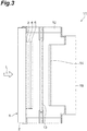
- the above-described photoelectric surface 1 is used for an image intensifier 11 shown in Fig. 3.
- Fig. 3 shows a structure of the image intensifier 11 including the photoelectric surface 1.
- the short-range image intensifier 11 includes the photoelectric surface 1, a vacuum container 12, a microchannel plate 13, a fluorescent surface 14, and an emission window material 16.
- the photoelectric surface 1 is provided on one end side of the vacuum container 12.
- the microchannel plate 13, which is electron multiplier means is provided behind the photoelectric surface 1.
- the fluorescent surface 14 is provided further behind the microchannel plate 13.
- the electrons multiplied by the microchannel plate 13 are incident to the fluorescent surface 14.
- the incident electrons are converted into light.
- the converted light is emitted to the outside through the emission window material 16.
- the image intensifier 11 includes the above-described photoelectric surface 1, it is possible to improve the sensitivity in an ultraviolet band.
- Example 1 the sensitivity of the photoelectric surface 1 was confirmed.
- quantum efficiency was adopted.
- the quantum efficiency is a ratio of the number of photoelectrons with respect to the number of photons incident to the photoelectric surface 1.
- the quantum efficiency is measured by, for example, a spectral sensitivity measurement device.
- the spectral sensitivity measurement device has a light source, a spectroscope which monochromates measurement target light, and a set standard light detector (for example, silicon photodiode).
- the photoelectric surface 1 according to Example 1 has the following constitution. In Example 1, a plurality of photoelectric surfaces 1 having the following constitution were prepared and the quantum efficiency of each of the photoelectric surfaces 1 was measured.
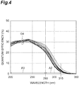
- Fig. 4 shows a relationship between the detection wavelength and the quantum efficiency of each photoelectric surface 1.
- the horizontal axis represents the wavelength and the vertical axis represents the quantum efficiency.
- a plurality of graphs G4 show the quantum efficiency of each photoelectric surface 1.
- each photoelectric surface 1 had a quantum efficiency of about from 2% to 26% in a band A2 ranging from 280 nm to 315 nm.
- photoelectric surface 1 had a quantum efficiency of about from 20% to 32% in a band A3 ranging from 200 nm to 280 nm.
- photoelectric surface had a quantum efficiency of about from 20% to 26% at a wavelength of 280 nm.
- Example 2 the effect of the film thickness of the intermediate film 4 on the quantum efficiency was confirmed. Specifically, a plurality of photoelectric surfaces 1 having intermediate films 4 with only different thicknesses were prepared and the quantum efficiency of the respective photoelectric surfaces 1 was measured.
- the photoelectric surface 1 according to Example 2 has the following constitution.
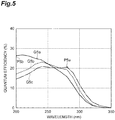
- the graph G5a in Fig. 5 shows the quantum efficiency of the photoelectric surface 1 in which the film thickness of the intermediate film 4 is 50 nm.
- the graph G5b shows the quantum efficiency of the photoelectric surface 1 in which the film thickness of the intermediate film 4 is 10 nm.
- the graph G5c shows the quantum efficiency of the photoelectric surface 1 in which the film thickness of the intermediate film 4 is 5 nm. According to graphs G5a, G5b, and G5c, it was found that in a wavelength band ranging from 200 nm to 280 nm, the magnitude relation of the quantum efficiency changed according to the film thickness of the intermediate film 4.
- the film thickness of the intermediate film 4 was made thin (refer to plot P5a).
- the thin film thickness is, for example, 5 nm. In other words, the thin film thickness is, for example, 50 ⁇ .
- the film thickness of the intermediate film 4 was made thick (refer to plot P5b).
- the thick film thickness is, for example, 50 nm. In other words, the thick film thickness is, for example, 500 ⁇ .
- Example 3 the effect of the constitution of the conductive film 3 on the quantum efficiency was confirmed. Specifically, a plurality of photoelectric surfaces 1 having conductive films 3 of different materials or structures from each other were prepared and the quantum efficiency of the respective photoelectric surfaces 1 was measured.
- the photoelectric surface 1 according to Example 3 has the following constitution.
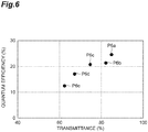
- Fig. 6 shows the quantum efficiency of each photoelectric surface 1 with respect to a wavelength of 280 nm.
- the vertical axis represents the quantum efficiency of the photoelectric surface 1.
- the horizontal axis represents the transmittance of the conductive film 3.
- the transmittance represented by the horizontal axis in Fig. 6 is an actually measured transmittance of each of test pieces in which various conductive films are formed on the window material 2 formed of a quartz surface plate.
- the transmittance is measured by a spectrophotometer or by transmittance measurement using a spectrophotometer including a light source, a spectroscope, and a light detector.
- the plot P6a shows the quantum conversion efficiency in the case in which the conductive film 3 is formed of graphene.
- the plot P6b shows the quantum conversion efficiency in the case in which the conductive film 3 has a stripe electrode structure.
- the plot P6c shows the quantum conversion efficiency in the case in which the conductive film 3 is formed of Ti (film thickness: 0.5 nm).
- the plot P6d shows the quantum conversion efficiency in the case in which the conductive film 3 is formed of Ti (film thickness: 2.5 nm).
- the plot P6e shows the quantum conversion efficiency in the case in which the conductive film 3 is formed of a carbon nanotube.
- Comparative Example 1 the effect of the constitutional material of the intermediate film 4 on the quantum efficiency was confirmed. Specifically, photoelectric surfaces having an intermediate film including an oxide were prepared and the quantum efficiency of each of the photoelectric surfaces was measured.
- the photoelectric surface according to Comparative Example 1 has the following constitution.
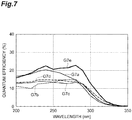
- Fig. 7 is a graph comparing the quantum efficiency of the photoelectric surface in Comparative Example 1 and the quantum efficiency of the photoelectric surface 1.
- the graph G7a shows the quantum efficiency of a photoelectric surface having an intermediate film having a two-layer structure.
- the intermediate film has a first layer formed of Al 2 O 3 and a second layer formed of ZnO.
- the graph G7b shows the quantum efficiency of a photoelectric surface having a conductive film formed of Ti and an intermediate film formed of Al 2 O 3 .
- the graph G7c shows the quantum efficiency of a photoelectric surface having a conductive film formed of Pt and an intermediate film formed of TiO 2 .
- the graph G7d shows the quantum efficiency of a photoelectric surface having a conductive film formed of Pt and an intermediate film formed of Al 2 O 3 .
- the graph G7e shows the quantum efficiency of the photoelectric surface 1 having an intermediate film 4 formed of MgF 2 . As shown in Fig. 7 , it was found that the graph G7e showed the highest quantum efficiency in a band of 200 nm or more and 350 nm or less. Accordingly, it was found that as the material forming the intermediate film 4, a fluoride was more preferable than an oxide.
- Comparative Example 2 the effect of the material forming the intermediate film 4 on the quantum efficiency was confirmed. Specifically, photoelectric surfaces having intermediate films formed of fluorides different from MgF 2 were prepared and the quantum efficiency of each of the photoelectric surfaces was measured. As fluorides different from MgF 2 , lithium fluoride (LiF) and calcium fluoride (CaF 2 ) were used.
- the photoelectric surface according to Comparative Example 2 has the following constitution.
- Fig. 8 is a graph comparing the quantum efficiency of the photoelectric surface in Comparative Example 2 and the quantum efficiency of the photoelectric surface 1.
- the graph G8a shows the quantum efficiency of the photoelectric surface 1 having an intermediate film 4 formed of LiF.
- the graph G8b shows the quantum efficiency of the photoelectric surface 1 having an intermediate film 4 formed of CaF 2 .
- the graph G8c shows the quantum efficiency of the photoelectric surface 1 having an intermediate film 4 formed of MgF 2 .
- the graph G8c showed the highest quantum efficiency in a band of 200 nm or more and 350 nm or less. Accordingly, it was found that it was most preferable that the intermediate film 4 was formed of MgF 2 out of the fluorides.
- the intermediate film 4 has a region having a high band gap formed near the photoelectric conversion film 6. Then, it is thought that as the band gap of the intermediate film 4 increases, the quantum efficiency of the photoelectric surface 1 increases.
- the band gap of each material used as the materials for the intermediate film 4, and the band gap of MgF 2 used as the material for the intermediate film 4 are as follows.
- Fig. 9 shows a relationship between the band gap and the quantum efficiency.
- the quantum efficiency in Fig. 9 is a value in the case of a detection wavelength of 280 nm.
- the following plots P9a, P9b, P9c, P9d, and P9e correspond to the plots P9a, P9b, P9c, P9d, and P9e in Fig. 9 .
- the present invention is not limited to the above-described embodiments and various modification can be made within a range not departing from the gist of the present invention.
- the material for forming the window material 2 calcium fluoride (CaF) and magnesium fluoride (MgF 2 ) may be used.
- the material for forming the conductive film 3 carbon-based materials such as graphene and carbon nanotube (CNT) may be used.
- the conductive film 3 may have a stripe structure or a mesh structure in consideration of light transmission.
- sodium (Ni), potassium (K), and rubidium (Rb) may be used as the alkali metal included in the photoelectric conversion film 6.
- the photoelectric surface is provided in the image intensifier, but the photoelectric surface may be used for optic devices other than the image intensifier.
- the photoelectric surface may be used for a photoelectric conversion tube or a photomultiplier tube.
- the photoelectric surface 1 shown in the above-described embodiment is provided in a vacuum container, and a dynode which becomes a multiplier which multiplies electrons or a microchannel plate is provided behind the photoelectric surface 1. Behind the dynode or microchannel plate, a positive electrode (anode) is provided in a state in which the positive electrode is accommodated in the vacuum container. To the positive electrode, a predetermined bias voltage is applied to the photoelectric surface, the electron multiplier, and the positive electrode through a lead pin. Then, the output signal from the positive electrode is output to the outside through the lead pin.
Landscapes
- Light Receiving Elements (AREA)
- Image-Pickup Tubes, Image-Amplification Tubes, And Storage Tubes (AREA)
- Physics & Mathematics (AREA)
- Electromagnetism (AREA)
- Photometry And Measurement Of Optical Pulse Characteristics (AREA)
Abstract
Description
- The present invention relates to a photoelectric surface, a photoelectric conversion tube having the photoelectric surface, an image intensifier, and a photomultiplier tube.
-
Patent Literatures Patent Literature 1 has a laminated structure in which a substrate, a base film, an intermediate film, and a photoelectric conversion film are laminated in this order. The photoelectric surfaces disclosed inPatent Literatures -
- [Patent Literature 1] Japanese Examined Patent Publication No.
H7-16016 - [Patent Literature 2] Japanese Unexamined Patent Publication No.
H6-68840 - [Patent Literature 3] Japanese Patent No.
4116294 - The photoelectric surfaces described in
Patent Literatures - In the technical field, it is desired to improve the sensitivity of the photoelectric surface in an ultraviolet band.
- According to a first aspect of the present invention, there is provided a photoelectric surface having a laminated structure including: a window material that transmits ultraviolet rays, a conductive film that is formed on the window material and has conductivity, an intermediate film that is formed on the conductive film and includes a compound of magnesium and fluorine, and a photoelectric conversion film that is formed on the intermediate film and includes tellurium and an alkali metal.
- Since the photoelectric conversion film of the photoelectric surface includes tellurium and an alkali metal, a wavelength band detected by the photoelectric surface can be set to an ultraviolet band including a solar blind band. In addition, the intermediate film including a compound of magnesium and fluorine is formed between the photoelectric conversion film and the conductive film. Since the intermediate film including a compound of magnesium and fluorine has a relatively large band gap, a film having a large band gap is disposed on the surface of the photoelectric conversion film on the side of the window material. Then, the curvature of the band occurs and the photoelectron extraction efficiency is improved. Thus, according to the photoelectric surface, it is possible to improve the sensitivity in an ultraviolet band.
- The compound may be magnesium fluoride and the alkali metal may be cesium. According to the constitutions thereof, since lattice mismatch generated between the photoelectric conversion film and the intermediate film is likely to be suppressed, it is possible to suppress a decrease in the crystallinity of the photoelectric conversion film. Accordingly, it is possible to further improve the sensitivity.
- In addition, the conductive film may include titanium. According to the constitution, the photoelectrons generated in the photoelectric conversion film can be efficiently extracted.
- The window material may include quartz. According to the constitution, since the attenuation of light occurring when the light passes through the window material is suppressed, it is possible to further improve the sensitivity.
- According to another aspect of the present invention, there is provided a photoelectric conversion tube including: a vacuum container that includes the photoelectric surface. Since the photoelectric conversion tube includes the photoelectric surface, it is possible to improve the sensitivity in an ultraviolet band.
- According to still another aspect of the present invention, there is provided an image intensifier including: a vacuum container that includes the photoelectric surface, electron multiplier means that is accommodated in the vacuum container and multiplies electrons emitted from the photoelectric conversion film, and a fluorescent surface onto which the electrons multiplied by the electron multiplier means are made incident and that converts the electrons multiplied by the electron multiplier means into light. Since the image intensifier includes the photoelectric surface, it is possible to improve the sensitivity in an ultraviolet band.
- According to still another aspect of the present invention, there is provided a photomultiplier tube including: a vacuum container that includes the photoelectric surface, electron multiplier means that is accommodated in the vacuum container and multiplies electrons emitted from the photoelectric conversion film, and an anode that is accommodated in the vacuum container and onto which the electrons multiplied by the electron multiplier means are made incident. Since the photomultiplier tube includes the photoelectric surface, it is possible to improve the sensitivity in an ultraviolet band.
- According to the photoelectric surface according to one aspect, and the photoelectric conversion tube, the image intensifier, and the photomultiplier tube according to another aspects of the present invention, it is possible to improve sensitivity in an ultraviolet band.
-
- [
Fig. 1] Fig. 1 is a view showing a cross section of a photoelectric surface according to an embodiment of the present invention. - [
Fig. 2] Fig. 2 is a graph showing a relationship between a spectrum of sunlight and a spectrum of a detection band of the photoelectric surface. - [
Fig. 3] Fig. 3 is a view showing a structure of an image intensifier having the photoelectric surface. - [
Fig. 4] Fig. 4 is a graph showing a relationship between the detection wavelength and the quantum efficiency of each photoelectric surface according to Example 1. - [
Fig. 5] Fig. 5 is a graph showing a relationship between the transmittance of a conductive film and quantum efficiency according to Example 2. - [
Fig. 6] Fig. 6 is a graph showing a relationship between the transmittance of a conductive film and quantum efficiency according to Example 3. - [
Fig. 7] Fig. 7 is a graph showing a relationship between the detection wavelength and the quantum efficiency of each photoelectric surface according to Comparative Example 1. - [
Fig. 8] Fig. 8 is a graph showing a relationship between the detection wavelength and the quantum efficiency of each photoelectric surface according to Comparative Example 2. - [
Fig. 9] Fig. 9 is a graph showing a relationship between a band gap and quantum efficiency. - Hereinafter, embodiments for carrying out the present invention will be described in detail with reference to the attached drawings. The same elements are denoted with the same reference symbols in descriptions of the drawings, and overlapping description will thus be omitted.
- A
photoelectric surface 1 shown inFig. 1 detects light L in an ultraviolet band. The wavelength band of the light L detected by the photoelectric surface 1 (hereinafter, also referred to as a "detection band") is set to a wavelength band included in an ultraviolet band. Specifically, the detection band may be set to a wavelength of 200 nm or more and 350 nm or less included in a near ultraviolet band and may be further set to a wavelength of 260 nm or more and 300 nm or less. In addition, the detection band may be set to a band having a wavelength of 280 nm as the center. Particularly, the spectrum of the sunlight is very small in the band having a wavelength of 280 nm or less, so-called solar blind band. As shown inFig. 2 , the spectrum of the sunlight (refer to graph G2a) is very narrow in the range in which the wavelength is about 280 nm or less (refer to band A1). Accordingly, in the case in which the detection band (refer to graph G2b) is set to a wavelength of 280 nm or less, thephotoelectric surface 1 can be used for engine flare analysis or the like under the environment of sunlight. - As shown in
Fig. 1 , thephotoelectric surface 1 has a laminated structure. Thephotoelectric surface 1 includes awindow material 2, aconductive film 3, anintermediate film 4, and aphotoelectric conversion film 6, and these films are laminated in this order. Accordingly, the light L incident to thewindow material 2 passes through thewindow material 2, theconductive film 3, and theintermediate film 4, and then reaches thephotoelectric conversion film 6. - The
window material 2 is a substrate of thephotoelectric surface 1. Thewindow material 2 has anincident surface 2a onto which the light L is made incident, and arear surface 2b on the opposite side of theincident surface 2a. Thewindow material 2 has good transmission with respect to light in the detection band of thephotoelectric surface 1. Accordingly, thewindow material 2 is made of a material that allows transmittance of ultraviolet rays. As the material that allows transmittance of ultraviolet rays, quartz (SiO2) may be used. - The
conductive film 3 is formed on arear surface 2b of thewindow material 2. Theconductive film 3 has a front surface 3a which comes in contact with thewindow material 2 and a rear surface 3b on the opposite side of the front surface 3 a. Theconductive film 3 is a base film of thephotoelectric conversion film 6 with respect to thewindow material 2. In addition, theconductive film 3 transmits the light L incident to thewindow material 2 and supplies photoelectrons to be emitted in thephotoelectric conversion film 6. As a material for forming theconductive film 3, for example, a metallic material having conductivity such as titanium (Ti) may be used. In the case in which theconductive film 3 is formed of Ti, the film thickness may be 2 nm or more and 10 nm or less. In other words, the film thickness may be 20 Å or more and 100 Å or less. In addition, the film thickness may be 0.1 nm or more and 2 nm or less. In other words, the film thickness may be 1 Å or more and 20 Å or less. - The
intermediate film 4 is formed on the rear surface 3b of theconductive film 3. Theintermediate film 4 has asurface 4a which comes in contact with theconductive film 3 and aninterface 4b on the opposite side of thesurface 4a. Theintermediate film 4 is a base film of thephotoelectric conversion film 6 with respect to theconductive film 3. In addition, theintermediate film 4 transmits the light L incident to thewindow material 2 and forms a region having a high band gap on the side of asurface 6a of thephotoelectric conversion film 6. Theintermediate film 4 is formed of magnesium fluoride (MgF2) which is a compound of magnesium (Mg) and fluorine (F). The band gap of MgF2 is 11.4 eV. In addition, the film thickness of theintermediate film 4 is 0.5 nm or more and 5 nm or less). In order words, the film thickness of theintermediate film 4 is 5 Å or more and 50 Å or less. For example, in the case in which the detection band of thephotoelectric surface 1 is set to a band having a wavelength of 280 nm as the center, the film thickness of theintermediate film 4 may be set to 0.5 nm or more and 5 nm or less. In other words, the film thickness of theintermediate film 4 may be set to 5 Å or more and 50 Å or less. Theintermediate film 4 is formed by deposition or sputtering. - The
photoelectric conversion film 6 is formed at theinterface 4b of theintermediate film 4. Thephotoelectric conversion film 6 has thesurface 6a which comes into contact with theintermediate film 4. Thephotoelectric conversion film 6 produces photoelectrons by the incident light L. Thephotoelectric conversion film 6 is formed of a compound of tellurium (Te) and an alkali metal such as cesium-tellurium (CsTe). - Since the
photoelectric conversion film 6 of thephotoelectric surface 1 is formed of CsTe, the detection wavelength can be set to an ultraviolet band including a solar blind band. In addition, theintermediate film 4 formed of MgF2 is formed between thephotoelectric conversion film 6 and theconductive film 3. Since theintermediate film 4 has a relatively large band gap, a film having a large band gap is disposed on the surface of thephotoelectric conversion film 6 on the side of thewindow material 2. Then, the curvature of the band occurs, and the photoelectron extraction efficiency is improved. Thus, according to thephotoelectric surface 1, it is possible to improve the sensitivity in an ultraviolet band. - In the
photoelectric surface 1, theintermediate film 4 is formed of MgF2, and thephotoelectric conversion film 6 is formed of CsTe. According to the constitution, it is possible to suppress a decrease in the crystallinity of thephotoelectric conversion film 6 by suppressing lattice mismatch generated between thephotoelectric conversion film 6 and theintermediate film 4. Accordingly, it is possible to further improve the sensitivity of thephotoelectric surface 1. - Further, the
conductive film 3 is formed of titanium. According to the constitution, photoelectrons generated in thephotoelectric conversion film 6 can be efficiently extracted. - The
window material 2 is formed of quartz. According to the constitution, since the attenuation of the light L occurring when the light passes through thewindow material 2 is suppressed, it is possible to further improve the sensitivity of thephotoelectric surface 1. - The above-described
photoelectric surface 1 is used for animage intensifier 11 shown inFig. 3. Fig. 3 shows a structure of theimage intensifier 11 including thephotoelectric surface 1. As shown inFig. 3 , the short-range image intensifier 11 includes thephotoelectric surface 1, avacuum container 12, amicrochannel plate 13, afluorescent surface 14, and anemission window material 16. Thephotoelectric surface 1 is provided on one end side of thevacuum container 12. In addition, in thevacuum container 12, themicrochannel plate 13, which is electron multiplier means, is provided behind thephotoelectric surface 1. Thefluorescent surface 14 is provided further behind themicrochannel plate 13. The electrons multiplied by themicrochannel plate 13 are incident to thefluorescent surface 14. In thefluorescent surface 14, the incident electrons are converted into light. The converted light is emitted to the outside through theemission window material 16. - Since the
image intensifier 11 includes the above-describedphotoelectric surface 1, it is possible to improve the sensitivity in an ultraviolet band. - In Example 1, the sensitivity of the
photoelectric surface 1 was confirmed. For the sensitivity of thephotoelectric surface 1, quantum efficiency was adopted. The quantum efficiency is a ratio of the number of photoelectrons with respect to the number of photons incident to thephotoelectric surface 1. The quantum efficiency is measured by, for example, a spectral sensitivity measurement device. The spectral sensitivity measurement device has a light source, a spectroscope which monochromates measurement target light, and a set standard light detector (for example, silicon photodiode). Thephotoelectric surface 1 according to Example 1 has the following constitution. In Example 1, a plurality ofphotoelectric surfaces 1 having the following constitution were prepared and the quantum efficiency of each of thephotoelectric surfaces 1 was measured. - Window material: quartz (film thickness: 5.94 mm)
- Conductive film: Ti (film thickness: 0.5 nm)
- Intermediate film: MgF2 (film thickness: 5 nm)
- Photoelectric conversion film: CsTe (film thickness: 10 nm)
-
Fig. 4 shows a relationship between the detection wavelength and the quantum efficiency of eachphotoelectric surface 1. The horizontal axis represents the wavelength and the vertical axis represents the quantum efficiency. A plurality of graphs G4 show the quantum efficiency of eachphotoelectric surface 1. As shown inFig. 4 , it could be confirmed that eachphotoelectric surface 1 had a quantum efficiency of about from 2% to 26% in a band A2 ranging from 280 nm to 315 nm. In addition, it could be confirmed thatphotoelectric surface 1 had a quantum efficiency of about from 20% to 32% in a band A3 ranging from 200 nm to 280 nm. Further, it could be confirmed that photoelectric surface had a quantum efficiency of about from 20% to 26% at a wavelength of 280 nm. - In Example 2, the effect of the film thickness of the
intermediate film 4 on the quantum efficiency was confirmed. Specifically, a plurality ofphotoelectric surfaces 1 havingintermediate films 4 with only different thicknesses were prepared and the quantum efficiency of the respectivephotoelectric surfaces 1 was measured. Thephotoelectric surface 1 according to Example 2 has the following constitution. - Window material: quartz (film thickness: 5.94 mm)
- Conductive film: Ti (film thickness: 0.5 nm)
- Intermediate film: MgF2 (film thickness: 50 nm, 10 nm, 5 nm, in other words, film thickness: 500 Å, 100 Å, 50 Å)
- Photoelectric conversion film: CsTe (film thickness: 10 nm)
- The graph G5a in
Fig. 5 shows the quantum efficiency of thephotoelectric surface 1 in which the film thickness of theintermediate film 4 is 50 nm. The graph G5b shows the quantum efficiency of thephotoelectric surface 1 in which the film thickness of theintermediate film 4 is 10 nm. The graph G5c shows the quantum efficiency of thephotoelectric surface 1 in which the film thickness of theintermediate film 4 is 5 nm. According to graphs G5a, G5b, and G5c, it was found that in a wavelength band ranging from 200 nm to 280 nm, the magnitude relation of the quantum efficiency changed according to the film thickness of theintermediate film 4. From the result, it was found that in the case in which the detection band of thephotoelectric surface 1 was set to a wavelength near 280 nm, it was preferable that the film thickness of theintermediate film 4 was made thin (refer to plot P5a). The thin film thickness is, for example, 5 nm. In other words, the thin film thickness is, for example, 50 Å. On the other hand, it was found that in the case in which the detection band of thephotoelectric surface 1 was set to a wavelength near 200 nm, it was preferable that the film thickness of theintermediate film 4 was made thick (refer to plot P5b). The thick film thickness is, for example, 50 nm. In other words, the thick film thickness is, for example, 500 Å. - In Example 3, the effect of the constitution of the
conductive film 3 on the quantum efficiency was confirmed. Specifically, a plurality ofphotoelectric surfaces 1 havingconductive films 3 of different materials or structures from each other were prepared and the quantum efficiency of the respectivephotoelectric surfaces 1 was measured. Thephotoelectric surface 1 according to Example 3 has the following constitution. - Window material: quartz (film thickness: 5.94 mm)
- Conductive film: Ti (film thickness: 0.5 nm), Ti (film thickness: 2.5 nm), carbon nanotube (film thickness: 1 nm), graphene (film thickness: 0.335 nm), stripe electrode (film thickness: 2.5 nm)
- Intermediate film: MgF2 (film thickness: 5 nm)
- Photoelectric conversion film: CsTe (film thickness: 10 nm)
-
Fig. 6 shows the quantum efficiency of eachphotoelectric surface 1 with respect to a wavelength of 280 nm. The vertical axis represents the quantum efficiency of thephotoelectric surface 1. The horizontal axis represents the transmittance of theconductive film 3. The transmittance represented by the horizontal axis inFig. 6 is an actually measured transmittance of each of test pieces in which various conductive films are formed on thewindow material 2 formed of a quartz surface plate. The transmittance is measured by a spectrophotometer or by transmittance measurement using a spectrophotometer including a light source, a spectroscope, and a light detector. InFig. 6 , the plot P6a shows the quantum conversion efficiency in the case in which theconductive film 3 is formed of graphene. The plot P6b shows the quantum conversion efficiency in the case in which theconductive film 3 has a stripe electrode structure. The plot P6c shows the quantum conversion efficiency in the case in which theconductive film 3 is formed of Ti (film thickness: 0.5 nm). The plot P6d shows the quantum conversion efficiency in the case in which theconductive film 3 is formed of Ti (film thickness: 2.5 nm). The plot P6e shows the quantum conversion efficiency in the case in which theconductive film 3 is formed of a carbon nanotube. As shown by plots P6a, P6b, P6c, P6d, and P6e, it was found that as the transmittance of theconductive film 3 increased, the quantum efficiency increased. Particularly, in the case in which theconductive film 3 was graphene, a stripe electrode, or Ti having a film thickness of 0.5 nm, a quantum efficiency of 20% or more could be obtained at a wavelength of 280 nm. - In Comparative Example 1, the effect of the constitutional material of the
intermediate film 4 on the quantum efficiency was confirmed. Specifically, photoelectric surfaces having an intermediate film including an oxide were prepared and the quantum efficiency of each of the photoelectric surfaces was measured. The photoelectric surface according to Comparative Example 1 has the following constitution. - Window material: quartz (film thickness: 5.94 mm)
- Conductive film: Ti (film thickness: 2.5 nm), Pt (film thickness: 2.5 nm)
- Intermediate film: two-layer structure (first layer: Al2O3, second layer: ZnO), Al2O3 with a conductive film formed of Ti, TiO2, Al2O3 with a conductive film formed of Pt
- Photoelectric conversion film: CsTe (film thickness: 10 nm)
-
Fig. 7 is a graph comparing the quantum efficiency of the photoelectric surface in Comparative Example 1 and the quantum efficiency of thephotoelectric surface 1. The graph G7a shows the quantum efficiency of a photoelectric surface having an intermediate film having a two-layer structure. The intermediate film has a first layer formed of Al2O3 and a second layer formed of ZnO. The graph G7b shows the quantum efficiency of a photoelectric surface having a conductive film formed of Ti and an intermediate film formed of Al2O3. The graph G7c shows the quantum efficiency of a photoelectric surface having a conductive film formed of Pt and an intermediate film formed of TiO2. The graph G7d shows the quantum efficiency of a photoelectric surface having a conductive film formed of Pt and an intermediate film formed of Al2O3. The graph G7e shows the quantum efficiency of thephotoelectric surface 1 having anintermediate film 4 formed of MgF2. As shown inFig. 7 , it was found that the graph G7e showed the highest quantum efficiency in a band of 200 nm or more and 350 nm or less. Accordingly, it was found that as the material forming theintermediate film 4, a fluoride was more preferable than an oxide. - In Comparative Example 2, the effect of the material forming the
intermediate film 4 on the quantum efficiency was confirmed. Specifically, photoelectric surfaces having intermediate films formed of fluorides different from MgF2 were prepared and the quantum efficiency of each of the photoelectric surfaces was measured. As fluorides different from MgF2, lithium fluoride (LiF) and calcium fluoride (CaF2) were used. The photoelectric surface according to Comparative Example 2 has the following constitution. - Window material: quartz (film thickness: 5.94 mm)
- Conductive film: Ti (film thickness: 2.5 nm)
- Intermediate film: LiF (film thickness: 5 nm), CaF2 (film thickness: 5 nm)
- Photoelectric conversion film: CsTe (film thickness: 10 nm)
-
Fig. 8 is a graph comparing the quantum efficiency of the photoelectric surface in Comparative Example 2 and the quantum efficiency of thephotoelectric surface 1. The graph G8a shows the quantum efficiency of thephotoelectric surface 1 having anintermediate film 4 formed of LiF. The graph G8b shows the quantum efficiency of thephotoelectric surface 1 having anintermediate film 4 formed of CaF2. The graph G8c shows the quantum efficiency of thephotoelectric surface 1 having anintermediate film 4 formed of MgF2. As shown inFig. 8 , it was found that the graph G8c showed the highest quantum efficiency in a band of 200 nm or more and 350 nm or less. Accordingly, it was found that it was most preferable that theintermediate film 4 was formed of MgF2 out of the fluorides. - Incidentally, the
intermediate film 4 has a region having a high band gap formed near thephotoelectric conversion film 6. Then, it is thought that as the band gap of theintermediate film 4 increases, the quantum efficiency of thephotoelectric surface 1 increases. In Comparative Examples 1 and 2, the band gap of each material used as the materials for theintermediate film 4, and the band gap of MgF2 used as the material for theintermediate film 4 are as follows. In addition,Fig. 9 shows a relationship between the band gap and the quantum efficiency. The quantum efficiency inFig. 9 is a value in the case of a detection wavelength of 280 nm. The following plots P9a, P9b, P9c, P9d, and P9e correspond to the plots P9a, P9b, P9c, P9d, and P9e inFig. 9 . - MgF2 (plot P9a): 11.4 eV
- LiF (plot P9b): 13.8 eV
- CaF2 (plot P9c): 11.0 eV
- Al2O3 (plot P9d): 7.5 eV
- TiO2 (plot P9e): 3.2 eV
- With reference to
Fig. 9 , it was found that a positive correlation was established between the band gap and the quantum efficiency. On the other hand, it was found that when attention was paid to MgF2 (plot P9a) and LiF (plot P9b), MgF2 having a small band gap exhibited a higher quantum efficiency than LiF. The reason is presumed that factors other than the band gap of the intermediate film are involved in the quantum efficiency. Examples thereof include the effect of the intermediate film on the crystallinity of the photoelectric conversion film. It is presumed that the relation of band gap, crystallinity, or the like comprehensively works between the intermediate film and the photoelectric conversion film to determine the quantum efficiency. - The present invention is not limited to the above-described embodiments and various modification can be made within a range not departing from the gist of the present invention.
- For example, as the material for forming the
window material 2, calcium fluoride (CaF) and magnesium fluoride (MgF2) may be used. In addition, as the material for forming theconductive film 3, carbon-based materials such as graphene and carbon nanotube (CNT) may be used. Further, theconductive film 3 may have a stripe structure or a mesh structure in consideration of light transmission. In addition, as the alkali metal included in thephotoelectric conversion film 6, sodium (Ni), potassium (K), and rubidium (Rb) may be used. - Further, in the above-describe embodiment, the photoelectric surface is provided in the image intensifier, but the photoelectric surface may be used for optic devices other than the image intensifier. For example, the photoelectric surface may be used for a photoelectric conversion tube or a photomultiplier tube. In this case, the
photoelectric surface 1 shown in the above-described embodiment is provided in a vacuum container, and a dynode which becomes a multiplier which multiplies electrons or a microchannel plate is provided behind thephotoelectric surface 1. Behind the dynode or microchannel plate, a positive electrode (anode) is provided in a state in which the positive electrode is accommodated in the vacuum container. To the positive electrode, a predetermined bias voltage is applied to the photoelectric surface, the electron multiplier, and the positive electrode through a lead pin. Then, the output signal from the positive electrode is output to the outside through the lead pin. -
- 1 ... PHOTOELECTRIC SURFACE, 2 ... WINDOW MATERIAL, 3 ... CONDUCTIVE FILM, 4 ... INTERMEDIATE FILM, 6 ... PHOTOELECTRIC CONVERSION FILM, 11 ... IMAGE INTENSIFIER, 12 ... VACUUM CONTAINER, 13 ... MICROCHANNEL PLATE (ELECTRON MULTIPLIER MEANS), 14 ... FLUORESCENT SURFACE, 16 ... EMISSION WINDOW MATERIAL
Claims (8)
- A photoelectric surface having a laminated structure comprising:a window material that transmits ultraviolet rays;a conductive film that is formed on the window material and has conductivity;an intermediate film that is formed on the conductive film and includes a compound of magnesium and fluorine; anda photoelectric conversion film that is formed on the intermediate film and includes tellurium and an alkali metal.
- The photoelectric surface according to claim 1,wherein the compound is magnesium fluoride.
- The photoelectric surface according to claim 1 or 2,wherein the alkali metal is cesium.
- The photoelectric surface according to any one of claims 1 to 3,wherein the conductive film includes titanium.
- The photoelectric surface according to any one of claims 1 to 4,wherein the window material includes quartz.
- A photoelectric conversion tube comprising:a vacuum container that includes the photoelectric surface according to any one of claims 1 to 5.
- An image intensifier comprising:a vacuum container that includes the photoelectric surface according to any one of claims 1 to 5;electron multiplier means that is accommodated in the vacuum container and multiplies electrons emitted from the photoelectric conversion film; anda fluorescent surface onto which the electrons multiplied by the electron multiplier means are incident and that convert the electrons multiplied by the electron multiplier means into light.
- A photomultiplier tube comprising:a vacuum container that includes the photoelectric surface according to any one of claims 1 to 5;electron multiplier means that is accommodated in the vacuum container and multiplies electrons emitted from the photoelectric conversion film; andan anode that is accommodated in the vacuum container and onto which the electrons multiplied by the electron multiplier means are incident.
Applications Claiming Priority (2)
| Application Number | Priority Date | Filing Date | Title |
|---|---|---|---|
| JP2014264384A JP6419572B2 (en) | 2014-12-26 | 2014-12-26 | Photocathode, photoelectric conversion tube, image intensifier, and photomultiplier tube |
| PCT/JP2015/085037 WO2016104243A1 (en) | 2014-12-26 | 2015-12-15 | Photoelectric surface, photoelectric conversion tube, image intensifier, and photomultiplier tube |
Publications (3)
| Publication Number | Publication Date |
|---|---|
| EP3240009A1 true EP3240009A1 (en) | 2017-11-01 |
| EP3240009A4 EP3240009A4 (en) | 2018-08-01 |
| EP3240009B1 EP3240009B1 (en) | 2019-09-25 |
Family
ID=56150268
Family Applications (1)
| Application Number | Title | Priority Date | Filing Date |
|---|---|---|---|
| EP15872812.1A Active EP3240009B1 (en) | 2014-12-26 | 2015-12-15 | Photoelectric surface, photoelectric conversion tube, image intensifier, and photomultiplier tube |
Country Status (7)
| Country | Link |
|---|---|
| US (1) | US10559445B2 (en) |
| EP (1) | EP3240009B1 (en) |
| JP (1) | JP6419572B2 (en) |
| KR (1) | KR102582084B1 (en) |
| CN (1) | CN107112175B (en) |
| ES (1) | ES2757377T3 (en) |
| WO (1) | WO2016104243A1 (en) |
Families Citing this family (6)
| Publication number | Priority date | Publication date | Assignee | Title |
|---|---|---|---|---|
| JP6401834B1 (en) * | 2017-08-04 | 2018-10-10 | 浜松ホトニクス株式会社 | Transmission type photocathode and electron tube |
| US10535493B2 (en) * | 2017-10-10 | 2020-01-14 | Kla-Tencor Corporation | Photocathode designs and methods of generating an electron beam using a photocathode |
| CN110854001B (en) * | 2019-11-13 | 2020-09-18 | 北方夜视技术股份有限公司 | Double-alkali photocathode with bowl-shaped energy band structure and preparation method thereof |
| CN111613497B (en) * | 2020-06-05 | 2023-05-12 | 陕西理工大学 | Spectral response enhanced transmission type photocathode and preparation method thereof |
| JP2022006920A (en) * | 2020-06-25 | 2022-01-13 | 浜松ホトニクス株式会社 | Photoelectric surface |
| CN113594003B (en) * | 2021-07-20 | 2023-07-21 | 北方夜视技术股份有限公司 | Cs of composite quartz window 2 Te solar blind ultraviolet photocathode and preparation method thereof |
Family Cites Families (17)
| Publication number | Priority date | Publication date | Assignee | Title |
|---|---|---|---|---|
| JPH0716016B2 (en) * | 1986-05-19 | 1995-02-22 | 富士通株式会社 | Infrared detector |
| JPH0716019B2 (en) * | 1991-03-04 | 1995-02-22 | 浜松ホトニクス株式会社 | Photocathode |
| JP2923395B2 (en) | 1992-08-24 | 1999-07-26 | 浜松ホトニクス株式会社 | Photocathode and photomultiplier tube |
| JP2886039B2 (en) | 1993-06-30 | 1999-04-26 | 株式会社クボタ | Combine harvesting stem and stem transport structure |
| JPH07160016A (en) | 1993-12-07 | 1995-06-23 | Matsushita Electric Ind Co Ltd | Multilayer type electrophotographic photoreceptor and paint for charge generation layer |
| SE0101864L (en) * | 2001-06-01 | 2002-12-02 | Xcounter Ab | Flame and spark detector, automatic fire alarm and related procedure |
| JP4116294B2 (en) * | 2002-01-07 | 2008-07-09 | 浜松ホトニクス株式会社 | Photocathode and photoelectric conversion tube |
| JP3869378B2 (en) * | 2003-03-12 | 2007-01-17 | 株式会社東芝 | Optical recording medium |
| KR100647305B1 (en) * | 2004-12-23 | 2006-11-23 | 삼성에스디아이 주식회사 | Optoelectronic device and lamp and display panel using same |
| JP4926504B2 (en) * | 2006-03-08 | 2012-05-09 | 浜松ホトニクス株式会社 | Photocathode, electron tube provided with the photocathode, and method for producing photocathode |
| JP2009272102A (en) * | 2008-05-02 | 2009-11-19 | Hamamatsu Photonics Kk | Photocathode and electron tube having the same |
| JP5308078B2 (en) * | 2008-06-13 | 2013-10-09 | 浜松ホトニクス株式会社 | Photocathode |
| US8581228B2 (en) * | 2009-01-22 | 2013-11-12 | Bae Systems Information And Electronic Systems Integration Inc. | Corner cube enhanced photocathode |
| JP2010286316A (en) * | 2009-06-10 | 2010-12-24 | Univ Of Tokyo | Photodetector |
| US9123622B2 (en) * | 2010-06-23 | 2015-09-01 | California Institute Of Technology | Atomic layer deposition of high performance anti reflection coatings on delta-doped CCDs |
| CN104871257B (en) * | 2012-12-17 | 2017-03-01 | 住友化学株式会社 | Zinc oxide transparent conductive film |
| WO2015014378A1 (en) * | 2013-07-31 | 2015-02-05 | Cern - European Organization For Nuclear Research | A detector and method for detecting ultraviolet radiation |
-
2014
- 2014-12-26 JP JP2014264384A patent/JP6419572B2/en active Active
-
2015
- 2015-12-15 KR KR1020177019010A patent/KR102582084B1/en active Active
- 2015-12-15 CN CN201580070708.7A patent/CN107112175B/en active Active
- 2015-12-15 US US15/538,693 patent/US10559445B2/en active Active
- 2015-12-15 WO PCT/JP2015/085037 patent/WO2016104243A1/en not_active Ceased
- 2015-12-15 ES ES15872812T patent/ES2757377T3/en active Active
- 2015-12-15 EP EP15872812.1A patent/EP3240009B1/en active Active
Also Published As
| Publication number | Publication date |
|---|---|
| WO2016104243A1 (en) | 2016-06-30 |
| EP3240009B1 (en) | 2019-09-25 |
| CN107112175A (en) | 2017-08-29 |
| JP2016126839A (en) | 2016-07-11 |
| US20180025881A1 (en) | 2018-01-25 |
| US10559445B2 (en) | 2020-02-11 |
| CN107112175B (en) | 2019-04-05 |
| JP6419572B2 (en) | 2018-11-07 |
| ES2757377T3 (en) | 2020-04-29 |
| EP3240009A4 (en) | 2018-08-01 |
| KR102582084B1 (en) | 2023-09-25 |
| KR20170099934A (en) | 2017-09-01 |
Similar Documents
| Publication | Publication Date | Title |
|---|---|---|
| EP3240009B1 (en) | Photoelectric surface, photoelectric conversion tube, image intensifier, and photomultiplier tube | |
| JP6595074B2 (en) | Photocathode comprising a silicon substrate with a boron layer | |
| JP6328225B2 (en) | Photomultiplier tube (PMT), image sensor, and inspection system using PMT or image sensor | |
| EP1939917A2 (en) | Photocathode, photomultiplier abnd electron tube | |
| CN101379582B (en) | Photoelectric surface, electron tube with the same, and method for manufacturing the photoelectric surface | |
| CN102067264B (en) | Photocathode | |
| JP5955713B2 (en) | Photocathode | |
| JP6324501B2 (en) | Inverse photoelectron spectrometer | |
| WO2004107378A2 (en) | Tuned bandwidth photocathode for transmission electron affinity devices | |
| EP0532358A1 (en) | Reflection type photocathode and photomultiplier using it | |
| US9818894B2 (en) | Photodetector with nanowire photocathode | |
| JP2023512183A (en) | Photomultiplier tube on gas electron multiplier substrate | |
| JP2018514063A (en) | Multi-band photocathode and related detector | |
| Costello et al. | Imaging GaAs vacuum photodiode with 40% quantum efficiency at 530 nm | |
| JP2651329B2 (en) | Cathode for photoelectron or secondary electron emission | |
| JP5865527B2 (en) | Photocathode and photomultiplier tube | |
| JP2009272102A (en) | Photocathode and electron tube having the same | |
| Rome | Multiplier Phototubes for the Far Ultraviolet | |
| RU2593648C1 (en) | Combined electro-optical converter | |
| Siegmund et al. | Development of sealed tube microchannel plate detectors with cross strip readouts | |
| Brooks et al. | Experimental data on the reflection and transmission spectral response of photocathodes | |
| JP2014044960A (en) | Photocathode | |
| Rome | in Imaging Devices |
Legal Events
| Date | Code | Title | Description |
|---|---|---|---|
| STAA | Information on the status of an ep patent application or granted ep patent |
Free format text: STATUS: THE INTERNATIONAL PUBLICATION HAS BEEN MADE |
|
| PUAI | Public reference made under article 153(3) epc to a published international application that has entered the european phase |
Free format text: ORIGINAL CODE: 0009012 |
|
| STAA | Information on the status of an ep patent application or granted ep patent |
Free format text: STATUS: REQUEST FOR EXAMINATION WAS MADE |
|
| 17P | Request for examination filed |
Effective date: 20170724 |
|
| AK | Designated contracting states |
Kind code of ref document: A1 Designated state(s): AL AT BE BG CH CY CZ DE DK EE ES FI FR GB GR HR HU IE IS IT LI LT LU LV MC MK MT NL NO PL PT RO RS SE SI SK SM TR |
|
| AX | Request for extension of the european patent |
Extension state: BA ME |
|
| DAV | Request for validation of the european patent (deleted) | ||
| DAX | Request for extension of the european patent (deleted) | ||
| A4 | Supplementary search report drawn up and despatched |
Effective date: 20180702 |
|
| RIC1 | Information provided on ipc code assigned before grant |
Ipc: H01J 40/06 20060101ALI20180626BHEP Ipc: H01J 31/50 20060101ALI20180626BHEP Ipc: H01J 29/38 20060101ALI20180626BHEP Ipc: H01J 1/34 20060101AFI20180626BHEP Ipc: H01J 1/78 20060101ALI20180626BHEP Ipc: H01J 40/16 20060101ALI20180626BHEP |
|
| GRAP | Despatch of communication of intention to grant a patent |
Free format text: ORIGINAL CODE: EPIDOSNIGR1 |
|
| STAA | Information on the status of an ep patent application or granted ep patent |
Free format text: STATUS: GRANT OF PATENT IS INTENDED |
|
| RIC1 | Information provided on ipc code assigned before grant |
Ipc: H01J 1/78 20060101ALI20190320BHEP Ipc: H01J 40/16 20060101ALI20190320BHEP Ipc: H01J 31/49 20060101ALN20190320BHEP Ipc: H01J 40/06 20060101ALI20190320BHEP Ipc: H01J 31/50 20060101ALI20190320BHEP Ipc: H01J 1/34 20060101AFI20190320BHEP Ipc: H01J 29/38 20060101ALI20190320BHEP |
|
| INTG | Intention to grant announced |
Effective date: 20190410 |
|
| GRAS | Grant fee paid |
Free format text: ORIGINAL CODE: EPIDOSNIGR3 |
|
| GRAA | (expected) grant |
Free format text: ORIGINAL CODE: 0009210 |
|
| STAA | Information on the status of an ep patent application or granted ep patent |
Free format text: STATUS: THE PATENT HAS BEEN GRANTED |
|
| AK | Designated contracting states |
Kind code of ref document: B1 Designated state(s): AL AT BE BG CH CY CZ DE DK EE ES FI FR GB GR HR HU IE IS IT LI LT LU LV MC MK MT NL NO PL PT RO RS SE SI SK SM TR |
|
| REG | Reference to a national code |
Ref country code: GB Ref legal event code: FG4D |
|
| REG | Reference to a national code |
Ref country code: CH Ref legal event code: EP |
|
| REG | Reference to a national code |
Ref country code: AT Ref legal event code: REF Ref document number: 1184659 Country of ref document: AT Kind code of ref document: T Effective date: 20191015 |
|
| REG | Reference to a national code |
Ref country code: IE Ref legal event code: FG4D |
|
| REG | Reference to a national code |
Ref country code: DE Ref legal event code: R096 Ref document number: 602015038857 Country of ref document: DE |
|
| REG | Reference to a national code |
Ref country code: NL Ref legal event code: FP |
|
| PG25 | Lapsed in a contracting state [announced via postgrant information from national office to epo] |
Ref country code: SE Free format text: LAPSE BECAUSE OF FAILURE TO SUBMIT A TRANSLATION OF THE DESCRIPTION OR TO PAY THE FEE WITHIN THE PRESCRIBED TIME-LIMIT Effective date: 20190925 Ref country code: BG Free format text: LAPSE BECAUSE OF FAILURE TO SUBMIT A TRANSLATION OF THE DESCRIPTION OR TO PAY THE FEE WITHIN THE PRESCRIBED TIME-LIMIT Effective date: 20191225 Ref country code: LT Free format text: LAPSE BECAUSE OF FAILURE TO SUBMIT A TRANSLATION OF THE DESCRIPTION OR TO PAY THE FEE WITHIN THE PRESCRIBED TIME-LIMIT Effective date: 20190925 Ref country code: NO Free format text: LAPSE BECAUSE OF FAILURE TO SUBMIT A TRANSLATION OF THE DESCRIPTION OR TO PAY THE FEE WITHIN THE PRESCRIBED TIME-LIMIT Effective date: 20191225 Ref country code: FI Free format text: LAPSE BECAUSE OF FAILURE TO SUBMIT A TRANSLATION OF THE DESCRIPTION OR TO PAY THE FEE WITHIN THE PRESCRIBED TIME-LIMIT Effective date: 20190925 Ref country code: HR Free format text: LAPSE BECAUSE OF FAILURE TO SUBMIT A TRANSLATION OF THE DESCRIPTION OR TO PAY THE FEE WITHIN THE PRESCRIBED TIME-LIMIT Effective date: 20190925 |
|
| REG | Reference to a national code |
Ref country code: LT Ref legal event code: MG4D |
|
| PG25 | Lapsed in a contracting state [announced via postgrant information from national office to epo] |
Ref country code: LV Free format text: LAPSE BECAUSE OF FAILURE TO SUBMIT A TRANSLATION OF THE DESCRIPTION OR TO PAY THE FEE WITHIN THE PRESCRIBED TIME-LIMIT Effective date: 20190925 Ref country code: GR Free format text: LAPSE BECAUSE OF FAILURE TO SUBMIT A TRANSLATION OF THE DESCRIPTION OR TO PAY THE FEE WITHIN THE PRESCRIBED TIME-LIMIT Effective date: 20191226 Ref country code: RS Free format text: LAPSE BECAUSE OF FAILURE TO SUBMIT A TRANSLATION OF THE DESCRIPTION OR TO PAY THE FEE WITHIN THE PRESCRIBED TIME-LIMIT Effective date: 20190925 |
|
| REG | Reference to a national code |
Ref country code: AT Ref legal event code: MK05 Ref document number: 1184659 Country of ref document: AT Kind code of ref document: T Effective date: 20190925 |
|
| REG | Reference to a national code |
Ref country code: ES Ref legal event code: FG2A Ref document number: 2757377 Country of ref document: ES Kind code of ref document: T3 Effective date: 20200429 |
|
| PG25 | Lapsed in a contracting state [announced via postgrant information from national office to epo] |
Ref country code: AL Free format text: LAPSE BECAUSE OF FAILURE TO SUBMIT A TRANSLATION OF THE DESCRIPTION OR TO PAY THE FEE WITHIN THE PRESCRIBED TIME-LIMIT Effective date: 20190925 Ref country code: AT Free format text: LAPSE BECAUSE OF FAILURE TO SUBMIT A TRANSLATION OF THE DESCRIPTION OR TO PAY THE FEE WITHIN THE PRESCRIBED TIME-LIMIT Effective date: 20190925 Ref country code: EE Free format text: LAPSE BECAUSE OF FAILURE TO SUBMIT A TRANSLATION OF THE DESCRIPTION OR TO PAY THE FEE WITHIN THE PRESCRIBED TIME-LIMIT Effective date: 20190925 Ref country code: PL Free format text: LAPSE BECAUSE OF FAILURE TO SUBMIT A TRANSLATION OF THE DESCRIPTION OR TO PAY THE FEE WITHIN THE PRESCRIBED TIME-LIMIT Effective date: 20190925 Ref country code: RO Free format text: LAPSE BECAUSE OF FAILURE TO SUBMIT A TRANSLATION OF THE DESCRIPTION OR TO PAY THE FEE WITHIN THE PRESCRIBED TIME-LIMIT Effective date: 20190925 Ref country code: PT Free format text: LAPSE BECAUSE OF FAILURE TO SUBMIT A TRANSLATION OF THE DESCRIPTION OR TO PAY THE FEE WITHIN THE PRESCRIBED TIME-LIMIT Effective date: 20200127 |
|
| PG25 | Lapsed in a contracting state [announced via postgrant information from national office to epo] |
Ref country code: IS Free format text: LAPSE BECAUSE OF FAILURE TO SUBMIT A TRANSLATION OF THE DESCRIPTION OR TO PAY THE FEE WITHIN THE PRESCRIBED TIME-LIMIT Effective date: 20200224 Ref country code: CZ Free format text: LAPSE BECAUSE OF FAILURE TO SUBMIT A TRANSLATION OF THE DESCRIPTION OR TO PAY THE FEE WITHIN THE PRESCRIBED TIME-LIMIT Effective date: 20190925 Ref country code: SK Free format text: LAPSE BECAUSE OF FAILURE TO SUBMIT A TRANSLATION OF THE DESCRIPTION OR TO PAY THE FEE WITHIN THE PRESCRIBED TIME-LIMIT Effective date: 20190925 Ref country code: SM Free format text: LAPSE BECAUSE OF FAILURE TO SUBMIT A TRANSLATION OF THE DESCRIPTION OR TO PAY THE FEE WITHIN THE PRESCRIBED TIME-LIMIT Effective date: 20190925 |
|
| REG | Reference to a national code |
Ref country code: DE Ref legal event code: R097 Ref document number: 602015038857 Country of ref document: DE |
|
| PG2D | Information on lapse in contracting state deleted |
Ref country code: IS |
|
| PG25 | Lapsed in a contracting state [announced via postgrant information from national office to epo] |
Ref country code: DK Free format text: LAPSE BECAUSE OF FAILURE TO SUBMIT A TRANSLATION OF THE DESCRIPTION OR TO PAY THE FEE WITHIN THE PRESCRIBED TIME-LIMIT Effective date: 20190925 Ref country code: IS Free format text: LAPSE BECAUSE OF FAILURE TO SUBMIT A TRANSLATION OF THE DESCRIPTION OR TO PAY THE FEE WITHIN THE PRESCRIBED TIME-LIMIT Effective date: 20200126 |
|
| PLBE | No opposition filed within time limit |
Free format text: ORIGINAL CODE: 0009261 |
|
| REG | Reference to a national code |
Ref country code: CH Ref legal event code: PL |
|
| STAA | Information on the status of an ep patent application or granted ep patent |
Free format text: STATUS: NO OPPOSITION FILED WITHIN TIME LIMIT |
|
| REG | Reference to a national code |
Ref country code: BE Ref legal event code: MM Effective date: 20191231 |
|
| PG25 | Lapsed in a contracting state [announced via postgrant information from national office to epo] |
Ref country code: MC Free format text: LAPSE BECAUSE OF FAILURE TO SUBMIT A TRANSLATION OF THE DESCRIPTION OR TO PAY THE FEE WITHIN THE PRESCRIBED TIME-LIMIT Effective date: 20190925 |
|
| 26N | No opposition filed |
Effective date: 20200626 |
|
| PG25 | Lapsed in a contracting state [announced via postgrant information from national office to epo] |
Ref country code: LU Free format text: LAPSE BECAUSE OF NON-PAYMENT OF DUE FEES Effective date: 20191215 Ref country code: IE Free format text: LAPSE BECAUSE OF NON-PAYMENT OF DUE FEES Effective date: 20191215 |
|
| PG25 | Lapsed in a contracting state [announced via postgrant information from national office to epo] |
Ref country code: SI Free format text: LAPSE BECAUSE OF FAILURE TO SUBMIT A TRANSLATION OF THE DESCRIPTION OR TO PAY THE FEE WITHIN THE PRESCRIBED TIME-LIMIT Effective date: 20190925 Ref country code: BE Free format text: LAPSE BECAUSE OF NON-PAYMENT OF DUE FEES Effective date: 20191231 Ref country code: CH Free format text: LAPSE BECAUSE OF NON-PAYMENT OF DUE FEES Effective date: 20191231 Ref country code: LI Free format text: LAPSE BECAUSE OF NON-PAYMENT OF DUE FEES Effective date: 20191231 |
|
| PG25 | Lapsed in a contracting state [announced via postgrant information from national office to epo] |
Ref country code: CY Free format text: LAPSE BECAUSE OF FAILURE TO SUBMIT A TRANSLATION OF THE DESCRIPTION OR TO PAY THE FEE WITHIN THE PRESCRIBED TIME-LIMIT Effective date: 20190925 |
|
| PG25 | Lapsed in a contracting state [announced via postgrant information from national office to epo] |
Ref country code: MT Free format text: LAPSE BECAUSE OF FAILURE TO SUBMIT A TRANSLATION OF THE DESCRIPTION OR TO PAY THE FEE WITHIN THE PRESCRIBED TIME-LIMIT Effective date: 20190925 Ref country code: HU Free format text: LAPSE BECAUSE OF FAILURE TO SUBMIT A TRANSLATION OF THE DESCRIPTION OR TO PAY THE FEE WITHIN THE PRESCRIBED TIME-LIMIT; INVALID AB INITIO Effective date: 20151215 |
|
| PG25 | Lapsed in a contracting state [announced via postgrant information from national office to epo] |
Ref country code: TR Free format text: LAPSE BECAUSE OF FAILURE TO SUBMIT A TRANSLATION OF THE DESCRIPTION OR TO PAY THE FEE WITHIN THE PRESCRIBED TIME-LIMIT Effective date: 20190925 |
|
| PG25 | Lapsed in a contracting state [announced via postgrant information from national office to epo] |
Ref country code: MK Free format text: LAPSE BECAUSE OF FAILURE TO SUBMIT A TRANSLATION OF THE DESCRIPTION OR TO PAY THE FEE WITHIN THE PRESCRIBED TIME-LIMIT Effective date: 20190925 |
|
| P01 | Opt-out of the competence of the unified patent court (upc) registered |
Effective date: 20230509 |
|
| PGFP | Annual fee paid to national office [announced via postgrant information from national office to epo] |
Ref country code: NL Payment date: 20251112 Year of fee payment: 11 |
|
| PGFP | Annual fee paid to national office [announced via postgrant information from national office to epo] |
Ref country code: DE Payment date: 20251028 Year of fee payment: 11 |
|
| PGFP | Annual fee paid to national office [announced via postgrant information from national office to epo] |
Ref country code: GB Payment date: 20251030 Year of fee payment: 11 |
|
| PGFP | Annual fee paid to national office [announced via postgrant information from national office to epo] |
Ref country code: IT Payment date: 20251121 Year of fee payment: 11 |
|
| PGFP | Annual fee paid to national office [announced via postgrant information from national office to epo] |
Ref country code: FR Payment date: 20251110 Year of fee payment: 11 |
|
| PGFP | Annual fee paid to national office [announced via postgrant information from national office to epo] |
Ref country code: ES Payment date: 20260108 Year of fee payment: 11 |