EP3237996B1 - Thermal mitigation in devices with multiple processing units - Google Patents
Thermal mitigation in devices with multiple processing units Download PDFInfo
- Publication number
- EP3237996B1 EP3237996B1 EP15801587.5A EP15801587A EP3237996B1 EP 3237996 B1 EP3237996 B1 EP 3237996B1 EP 15801587 A EP15801587 A EP 15801587A EP 3237996 B1 EP3237996 B1 EP 3237996B1
- Authority
- EP
- European Patent Office
- Prior art keywords
- power supply
- real
- time
- pus
- switches
- Prior art date
- Legal status (The legal status is an assumption and is not a legal conclusion. Google has not performed a legal analysis and makes no representation as to the accuracy of the status listed.)
- Active
Links
Images



Classifications
-
- G—PHYSICS
- G06—COMPUTING OR CALCULATING; COUNTING
- G06F—ELECTRIC DIGITAL DATA PROCESSING
- G06F1/00—Details not covered by groups G06F3/00 - G06F13/00 and G06F21/00
- G06F1/26—Power supply means, e.g. regulation thereof
- G06F1/32—Means for saving power
- G06F1/3203—Power management, i.e. event-based initiation of a power-saving mode
- G06F1/3234—Power saving characterised by the action undertaken
- G06F1/3287—Power saving characterised by the action undertaken by switching off individual functional units in the computer system
-
- G—PHYSICS
- G06—COMPUTING OR CALCULATING; COUNTING
- G06F—ELECTRIC DIGITAL DATA PROCESSING
- G06F1/00—Details not covered by groups G06F3/00 - G06F13/00 and G06F21/00
- G06F1/16—Constructional details or arrangements
- G06F1/20—Cooling means
- G06F1/206—Cooling means comprising thermal management
-
- G—PHYSICS
- G06—COMPUTING OR CALCULATING; COUNTING
- G06F—ELECTRIC DIGITAL DATA PROCESSING
- G06F1/00—Details not covered by groups G06F3/00 - G06F13/00 and G06F21/00
- G06F1/26—Power supply means, e.g. regulation thereof
- G06F1/32—Means for saving power
- G06F1/3203—Power management, i.e. event-based initiation of a power-saving mode
- G06F1/3206—Monitoring of events, devices or parameters that trigger a change in power modality
-
- G—PHYSICS
- G06—COMPUTING OR CALCULATING; COUNTING
- G06F—ELECTRIC DIGITAL DATA PROCESSING
- G06F1/00—Details not covered by groups G06F3/00 - G06F13/00 and G06F21/00
- G06F1/26—Power supply means, e.g. regulation thereof
- G06F1/32—Means for saving power
- G06F1/3203—Power management, i.e. event-based initiation of a power-saving mode
- G06F1/3206—Monitoring of events, devices or parameters that trigger a change in power modality
- G06F1/3215—Monitoring of peripheral devices
-
- G—PHYSICS
- G06—COMPUTING OR CALCULATING; COUNTING
- G06F—ELECTRIC DIGITAL DATA PROCESSING
- G06F1/00—Details not covered by groups G06F3/00 - G06F13/00 and G06F21/00
- G06F1/26—Power supply means, e.g. regulation thereof
- G06F1/32—Means for saving power
- G06F1/3203—Power management, i.e. event-based initiation of a power-saving mode
- G06F1/3234—Power saving characterised by the action undertaken
- G06F1/325—Power saving in peripheral device
- G06F1/3278—Power saving in modem or I/O interface
-
- G—PHYSICS
- G06—COMPUTING OR CALCULATING; COUNTING
- G06F—ELECTRIC DIGITAL DATA PROCESSING
- G06F1/00—Details not covered by groups G06F3/00 - G06F13/00 and G06F21/00
- G06F1/26—Power supply means, e.g. regulation thereof
- G06F1/32—Means for saving power
- G06F1/3203—Power management, i.e. event-based initiation of a power-saving mode
- G06F1/3234—Power saving characterised by the action undertaken
- G06F1/3296—Power saving characterised by the action undertaken by lowering the supply or operating voltage
-
- H—ELECTRICITY
- H04—ELECTRIC COMMUNICATION TECHNIQUE
- H04W—WIRELESS COMMUNICATION NETWORKS
- H04W52/00—Power management, e.g. Transmission Power Control [TPC] or power classes
- H04W52/02—Power saving arrangements
- H04W52/0209—Power saving arrangements in terminal devices
- H04W52/0261—Power saving arrangements in terminal devices managing power supply demand, e.g. depending on battery level
- H04W52/0296—Power saving arrangements in terminal devices managing power supply demand, e.g. depending on battery level switching to a backup power supply
-
- Y—GENERAL TAGGING OF NEW TECHNOLOGICAL DEVELOPMENTS; GENERAL TAGGING OF CROSS-SECTIONAL TECHNOLOGIES SPANNING OVER SEVERAL SECTIONS OF THE IPC; TECHNICAL SUBJECTS COVERED BY FORMER USPC CROSS-REFERENCE ART COLLECTIONS [XRACs] AND DIGESTS
- Y02—TECHNOLOGIES OR APPLICATIONS FOR MITIGATION OR ADAPTATION AGAINST CLIMATE CHANGE
- Y02D—CLIMATE CHANGE MITIGATION TECHNOLOGIES IN INFORMATION AND COMMUNICATION TECHNOLOGIES [ICT], I.E. INFORMATION AND COMMUNICATION TECHNOLOGIES AIMING AT THE REDUCTION OF THEIR OWN ENERGY USE
- Y02D10/00—Energy efficient computing, e.g. low power processors, power management or thermal management
-
- Y—GENERAL TAGGING OF NEW TECHNOLOGICAL DEVELOPMENTS; GENERAL TAGGING OF CROSS-SECTIONAL TECHNOLOGIES SPANNING OVER SEVERAL SECTIONS OF THE IPC; TECHNICAL SUBJECTS COVERED BY FORMER USPC CROSS-REFERENCE ART COLLECTIONS [XRACs] AND DIGESTS
- Y02—TECHNOLOGIES OR APPLICATIONS FOR MITIGATION OR ADAPTATION AGAINST CLIMATE CHANGE
- Y02D—CLIMATE CHANGE MITIGATION TECHNOLOGIES IN INFORMATION AND COMMUNICATION TECHNOLOGIES [ICT], I.E. INFORMATION AND COMMUNICATION TECHNOLOGIES AIMING AT THE REDUCTION OF THEIR OWN ENERGY USE
- Y02D30/00—Reducing energy consumption in communication networks
- Y02D30/70—Reducing energy consumption in communication networks in wireless communication networks
Definitions
- This application relates to thermal mitigation in mobile devices, and more particularly, to thermal mitigation in mobile devices having multiple processing units.
- a mobile communications and computing device such as a smartphone or tablet computer
- multiple processing units PUs
- leakage current in a PU increases as temperature increases, thereby draining battery resources.
- a second reason relates to device preservation and user safety. For example, in some scenarios temperature can keep increasing to the point that the device not only reaches a point of failure wherein internal circuitry starts to malfunction but the device can also become hot enough to cause discomfort to a user. Accordingly, thermal mitigation is a long-standing issue that seeks to keep device temperature under control while maintaining satisfactory performance.
- One technique for performing thermal mitigation is to reduce voltage supplied to one or more PUs in a mobile device. Reducing voltage to a PU reduces power consumption which in turn reduces an amount of heat produced by the PU.
- a PU may be designed to operate at a lower speed, for example, as voltage is reduced, thus providing for a tradeoff between power consumption and performance.
- Digital circuits are usually integrated on semiconductor dies, and several PUs, such as a modem and a multi-core processor, may be present on a single semiconductor die in a mobile device.
- a system on chip refers to multiple PUs embedded on a single die.
- a PU is a functional block on the SoC.
- a PU may be a wireless baseband modem, a graphics processing unit (GPU), an image processing unit, a core in a multi-core processor, or other type of processing circuitry.
- the PUs in an SoC may encompass a wide variety of functional elements, and thus, their frequency and voltage requirements (e.g., related to desired performance) may differ vastly at any given moment. Therefore, in order to adequately perform thermal mitigation, one or more of these functional blocks may be independently operated such that their respective frequency and voltage values may be appropriately scaled.
- a voltage source controls the power supplied to a PU, and thus a voltage source is a type of power supply.
- any number of PUs can be supplied by any number of power supplies.
- the power supplies may be located off the SoC, resulting in excessive cost and/or pin count.
- a switched mode power supply (SMPS) is one such example.
- multiple SMPSs are part of a power management integrated circuit (PMIC).
- At least one of the independent power supplies may be located on the SoC, but the power supplies are sized such that power is supplied to all cores, and as a result occupy a large area of the die. There is therefore a need for mobile device architectures and methods that provide adequate thermal mitigation without incurring excessive penalties for cost or die area.
- Thermal mitigation generally entails taking one or more temperature measurements of a device and then taking various actions, if needed, in response to the measurements to reduce temperature of the device. One or more actions is performed and then a new temperature measurement is taken, and the process is repeated as needed in a feedback loop.
- a new architecture for delivering power to PUs is presented herein, and the new architecture provides for performing new thermal mitigation methods.
- Embodiments of the new architecture provide flexible, yet low cost ways to tradeoff performance and heat generation in devices having multiple non-real-time PUs.
- the performance of non-real-time PUs can be tuned to reduce power consumption and the corresponding generation of heat, while at the same time maintaining performance of real-time PUs.
- a method of performing thermal mitigation in a device having a plurality of non-real-time PUs and a plurality of real-time PUs includes connecting each of the plurality of real-time PUs and the plurality of non-real-time PUs to a first power supply, and performing thermal mitigation.
- Performing thermal mitigation includes disconnecting each of the plurality of non-real-time PUs except one of the plurality of non-real-time PUs from the first power supply resulting in an active non-real-time PU, and connecting a second power supply that derives power from the first power supply to the active non-real-time PU.
- a voltage supplied by the second power supply is less than a voltage supplied by the first power supply.
- an SoC in another embodiment, is disclosed.
- the SoC includes a voltage rail configured to couple to a first power supply, and a second power supply coupled to the voltage rail and configured to derive power from the first power supply.
- At least one real-time PU is coupled to the voltage rail via a switch.
- the SoC further includes a plurality of non-real-time PUs, a first plurality of switches, and a second plurality of switches.
- Each of the plurality of non-real-time PUs is coupled to the voltage rail via a parallel conductive path, with each parallel conductive path having a first path and a second path.
- the first path of each parallel connection includes a corresponding switch in the first plurality of switches
- the second path of each parallel connection includes a corresponding switch in the second plurality of switches connected in series with the second power supply.
- a device in yet another embodiment, includes a first power supply, a plurality of non-real-time PUs, first plurality of switches, a second plurality of switches, a second power supply that derives power from the first power supply, and a real-time PU connected to the first power supply.
- Each of the first plurality of switches is connected between at least one of the plurality of non-real-time PUs and the first power supply.
- Each of the second plurality of switches is connected between at least one of the plurality of non-real-time PUs and the second power supply.
- the device also has a thermal mitigation PU.
- the thermal mitigation PU is configured to control the first plurality of switches to successively open each of the first plurality of switches in response to successive temperature measurements of the device exceeding a threshold, and control the second plurality of switches to allow only one non-real-time PU to receive power from the second power supply while each of the first plurality of switches is open.
- the thermal mitigation PU is further configured to receive a first temperature measurement of the device, and in response to the first temperature measurement exceeding the threshold, control the second power supply to reduce the voltage supplied by the second power supply.
- a computer program product has a computer readable medium tangibly recording computer program logic for performing thermal mitigation in a device having a plurality of non-real-time PUs and a plurality of real-time PUs.
- the computer program product includes code to perform various actions, including connect each of the plurality of real-time PUs and the plurality of non-real-time PUs to a first power supply, and successively disconnect non-real-time PUs from the first power supply until only one non-real-time PU remains active. There is also code to obtain a first temperature measurement of the device, and determine that the first temperature measurement exceeds a threshold.
- Non-real-time PUs can be distinguished from real-time PUs for the purpose of thermal mitigation. For example, a degree of control of the non-real-time PUs is provided that is independent of the control of the real-time PUs. Thus, performance of the non-real-time PUs can be controlled in a manner separate from the real-time PUs. In order to reduce temperature of a device, a number of measures are provided which take advantage of the separate control of non-real-time PUs.
- Exemplary embodiments may employ one or more of the following measures for mitigating high temperatures in a device.
- the non-real-time PUs can be switched off until only one active non-real-time PU remains.
- the disclosed architectures are flexible to allow any non-real-time PU to be the remaining active PU. Further, the voltage provided to a remaining non-real-time PU can be reduced in order to reduce power consumption and heat generation of the non-real-time PU.
- any active software application running on an active non-real-time PU can be transferred to a non-active and cooler non-real-time PU that is chosen to be made active so that a non-real-time PU that has gotten too hot can be switched off
- These measures allow for a device to be cooled by reducing performance of PUs in such a way that user-perceived device performance is not significantly negatively affected. Furthermore, these measures can be implemented at low cost using a relatively small area of an SoC.
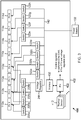
- Fig. 1 illustrates an embodiment of digital circuitry 200 having a power supply 132 and a corresponding supply rail 142.
- the digital circuitry 200 further includes a plurality of PUs 112a-112d coupled to power supply rail 142 via a plurality of corresponding switches 122a-122d, and a plurality of PUs 114a-114d coupled to the power supply rail 142 via a plurality of corresponding switches 122e-122h.
- a switch 122 allows its corresponding PU 112 or 114 to be disconnected from operation whenever desired, such as during periods when the PU is idle.
- each switch 122 is capable of handling high power from a power supply.
- each switch may be a type of head switch, such as a global distributed head switch (GDHS) or a block head switch (BHS). Disconnecting or removing a PU from operation temporarily is sometimes referred to as "hot plugging" and reduces the current consumption of the disconnected PU.
- GDHS global distributed head switch
- BHS block head switch
- Digital circuitry 200 further includes a voltage regulator 244 coupled to the power supply rail 142 as shown in Fig. 1 .
- power for the voltage regulator 244 is supplied by power supply 132.
- Voltage regulator 244 provides a way to vary the voltage supplied to one or more PUs 112 in the event that thermal mitigation is performed.
- the voltage regulator 244 is a second power supply that derives power from the first power supply 132.
- Each of PUs 112a-112d has a parallel conductive path to power supply 132.
- a first path of each parallel conductive path includes a switch 122 connected between the PU 112 and the power supply 132 and a second path includes a switch 234 connected in series with the voltage regulator 244.
- the power supply 132 can supply power to a PU 112 directly or by way of voltage regulator 244.
- a smartphone includes digital circuitry 200, and PUs 112a through 112d are cores in a quad-core application processor, and PUs 5 114a through 114d are other types of processing units, including a GPU, a wireless communications modem, an image processing unit, or other type of digital signal processor (DSP).
- DSP digital signal processor
- PUs 114 are real-time PUs
- PUs 112 are non-real-time PUs
- the two types of PUs are treated differently for the purposes of thermal mitigation.
- a real-time PU generally would significantly impact user experience if performance is reduced to reduce temperature
- a non-real-time PU generally would not significantly impact user experience if performance is reduced to reduce temperature.
- real-time PUs have timing constraints on when operations should be performed.
- real-time PUs are not usually implemented with mechanisms (e.g., larger buffers) that would accommodate significantly reduced performance.
- real-time PUs have timing requirements from the network side, so even if a real-time PU is equipped with jitter buffers or off-line processing modes to accommodate significantly reduced performance, advantage cannot be taken of these mechanisms because of hard timelines from a protocol and network perspective.
- non-real time PUs may not have the above-mentioned limitations.
- a wireless communications modem and graphics processor are examples of a real-time PU, and each core of a multi-core processor is an example non-real-time PU.
- a software application can execute using a plurality of cores for faster execution. More than one core at a time can execute instructions in parallel so that the application executes more quickly. The fewer the available cores, the more slowly an application will generally execute. The same is true for any application that is able to use a plurality of non-real-time PUs. That is, the fewer available non-real-time PUs, the more slowly an application for the non-real-time PUs will generally execute.
- PUs 112a-112d may be successively shut down via the corresponding switches 122a-122d until the temperature is below a second threshold.
- Logic to perform thermal mitigation is described in more detail with respect to Figs. 3 and 4 .
- one of PUs 112a-112d remains on, despite the hot plugging of the other PUs, to accommodate any applications.
- the application may have a memory state of the PU associated with program execution as well as instructions in a queue ready to be executed by the PU.
- the state of the application instructions (such as a thread or process) running on the PU is saved and application instructions queued to be executed by the PU that is to be shut down are moved to a queue or buffer of another active PU in such a way that the application keeps executing consistently and without crashing.
- movement of the instructions from one PU to another may be controlled by a scheduler in the operating system.
- voltage regulator 244 is activated to provide power to that PU 112 through an appropriate one of the switches 234a-234d. At that point, voltage regulator 244 can be used to reduce the voltage supplied to the remaining PU 112 in an attempt to further reduce temperature.
- PU rotation can be performed in which a different one of PUs 112a-112d is turned on via its corresponding switch 112 and the current one of PUs 112a-1 12d is switched off via its corresponding switch 112.
- the extra set of switches 234 allow PU rotation of the PU whose voltage is regulated by the voltage regulator 244.
- PU rotation includes the process of selecting and re-selecting an active PU from a multiplicity of PUs.
- PU rotation can be accomplished in a manner similar to that described above for shutting down PUs, except that only one PU is powered on and available to execute instructions.
- an active PU has corresponding instructions queued and ready to be executed and a current state of the application stored in memory. When a different PU is made active, the instructions are moved to a queue for the new PU and the application state is maintained for the new PU.
- a device operating system can manage the application during rotation. In the embodiment of Fig. 1 , the rotation is managed by switching on only one of switches 234a-234d at a time. The switches 122a-122d are turned off and remain off during PU rotation.
- An inactive PU that has been idle for some time may be cooler than the currently active PU.
- Making an inactive PU newly active and shutting off the currently active PU is a way to reduce temperature of a device.
- the temperature of the newly active PU may be below a temperature threshold, while the temperature of the active PU that is shut off may be above a temperature threshold.
- the "rotation" of PUs refers to the pattern of moving the active state or "on state" from one PU to another until temperature is under control.
- the rotation may be accomplished in a number of ways.
- the rotation may be in a predetermined order, such as a round-robin order.
- the active state may be transferred from PU 112a to PU 112b to PU 112c to PU 112d to PU 112a and so on in a fixed order.
- the rotation may be in an order determined based on a condition, such as the temperature of the PUs. For example, the coolest PU may be selected to be the next active PU.
- the voltage regulator 244 can be placed on an SoC die along with switches 122 and 234 and PUs 112 and 114, with the power supply 132 being located off-die.
- the voltage regulator 244 is sized to supply current to only one core at a time. The cost savings of one power supply 132 more than offsets the added cost of the voltage regulator 244. This is due at least in part to the voltage regulator 244 being a different class of voltage regulator than power supply 132 and also the voltage regulator 244 being dimensioned to power only one core.
- the voltage regulator 244 is a low-drop out (LDO) voltage regulator
- the power supply 132 is an SMPS.
- An LDO voltage regulator is a type of linear regulator that can operate with a small input-to-output differential voltage.
- An LDO provides high efficiency and low heat dissipation.
- An SMPS is generally a more complex type of voltage regulator than an LDO.
- An SMPS typically includes passive components, such as an inductor and a capacitor, not included in an LDO.
- a pass transistor is operated in a switching mode instead of a linear mode, as in an LDO.
- a pass transistor is either in an on state or an off state. Due to its smaller area and lack of passive components, generally an LDO can more readily be implemented in an SoC than can an SMPS.
- FIG. 2 A flow diagram of an example method 300 of performing thermal mitigation using digital circuitry, such as digital circuitry 200, is shown in Fig. 2.
- Fig. 2 is described with reference to Fig. 3 , which illustrates an embodiment of a device 400 including the components illustrated in Fig. 1 together with one or more thermal sensors 412, a PU 422, and memory 432.
- the device includes an SoC 402 and power supply 132.
- the SoC 402 does not include the power supply 132, although in other embodiments the power supply 132 may be integrated into the SoC 402.
- the SoC 402 is configured to couple to a power supply, such as power supply 132.
- the SoC 402 includes a multi-core processor having a plurality of cores represented by PUs 112a-112d.
- the one or more thermal sensors 412 provide an indication, either directly or indirectly, of temperature at one or more locations on the device 400.
- the one or more thermal sensors 412 communicate at least one signal indicating temperature to a PU, such as PU 422.
- the PU 422 implements one or more actions in response to the temperature indication in order to affect temperature of the device 400.
- the thermal sensors 412 together with PU 422 may be viewed as implementing a feedback loop in which the PU 422 keeps track of temperature and performs thermal mitigation as appropriate.
- the memory 432 may be any electronic component capable of storing information and/or instructions.
- the memory 432 may include random access memory (RAM), read-only memory (ROM), flash memory devices in RAM, optical storage media, erasable programmable read-only memory (EPROM), registers, or combinations thereof.
- the memory 432 is a non-transitory computer-readable medium. Instructions or code may be stored in the memory 432 that are executable by the PU 422 to implement the method 300.
- the PU 422 may be referred to herein as a thermal mitigation PU.
- the terms "instructions" and "code” should be interpreted broadly to include any type of computer-readable statement(s).
- instructions and code may refer to one or more programs, routines, sub-routines, functions, procedures, etc.
- Instructions and code may include a single computer-readable statement or many computer-readable statements.
- instructions for implementing the method 300 may be executed in the PU 422.
- the PU 422 is coupled to switches 232 and 234 and controls the states of the switches via one or more control signals.
- the PU 422 is also coupled to the voltage regulator 244 to control the voltage provided by the voltage regulator 244.
- one of the PUs 112 is designated as implementing the method 300, in which case the PU 112 that implements the method 300 remains connected to power supply 132 at all times and is not considered as part of the thermal mitigation method 300 itself.
- the example method 300 begins in block 310 in which the device 400 is in normal mode.
- Normal mode is a device state in which no thermal mitigation is being performed.
- a device in normal mode measures temperature at one or more locations on the device at predetermined time intervals (e.g., one measurement per minute, per 10 seconds, or per second).
- time intervals e.g., one measurement per minute, per 10 seconds, or per second.
- each of the switches 222 and 232 are closed so that each of the PUs 112 and 114 are connected to the power supply 132, and each of the switches 234 are open.
- the power supply 132 is providing power directly to each of the PUs 112 and 114.
- a temperature measurement of the device 400 is obtained in block 312.
- the temperature measurement may be performed by one or more thermal sensors 412, with the temperature measurement provided to a PU, such as PU 422. If more than one temperature measurement is taken, the measurements may be averaged or any other statistical measure may be used to produce a single number or multiple numbers referred to as the temperature measurement.
- an active PU is both connected to power and is not idle (e.g., is executing application instructions).
- the PUs 112 are cores in a multi-core processor or any other type of non-real-time PU, whereas the PUs 114 are real-time PUs that stay connected to power supply 132
- the method 300 proceeds to block 325 in which an active PU 112 is disconnected or hot plugged by opening or shutting off its corresponding switch 232.
- the method 300 may further include saving the processing state of the active PU 112 and transferring its state to a remaining active PU 112 to allow the remaining active PU 112 to take over processing.
- the method 300 may further include moving the instructions that are buffered for the active PU 112 to be shut down to a buffer or queue for a selected active PU 112 to take over processing these instructions.
- the PU 422 generates one or more control signals coupled to switches 122 to open any selected switches of switches 122a-122d in order to disconnect a PU 112.
- the temperature T of the device is obtained in block 328 from sensors 412 and compared, by PU 422, to a second threshold T th_low in decision block 330. If T is less than T th_low then PU 422 returns the device 400 to its normal mode 310 by opening all switches 234 and closing all switches 122. However, if Tis not less than T th_low the method proceeds to decision block 335.
- the thresholds satisfy T th_high > T th_low to help prevent the method 300 from oscillating between the normal mode and thermal mitigation.
- a number of active PUs 112 is determined by PU 422. If the number of active PUs 112 is greater than 1 then the method returns to block 325. If the number of active PUs 112 is equal to 1, then the method proceeds to block 340. Thus, in the series of actions or blocks 325 through 335, PUs 112 are successively disconnected from the power supply 132 until only one PU 112 is active or connected to the power supply 132. At that point, PU 422 takes other measures for thermal mitigation starting in block 340.
- a second power supply is connected to the active PU.
- the second power supply is the voltage regulator 244, and the voltage regulator 244 is connected to the active PU 112 by switching off the only remaining one of switches 122a-122d that is still on and switching on a switch in switches 234a-234d that corresponds to the active PU 112.
- Each PU 112a-112 has two parallel conductive paths to power supply 132.
- one conductive path includes switch 234a in series with voltage regulator 244, and the other conductive path includes switch 122a.
- switch 122a is switched off and switch 234a is switched on.
- the second power supply derives its power from a first power supply.
- the voltage regulator 244 derives its power from power supply 132.
- the voltage regulator 244 can be dimensioned to supply power to only a single PU thereby resulting in a voltage regulator 244 that occupies a small area of a die.
- the voltage supplied to the active PU is reduced in block 345. After a period of time has elapsed to allow the voltage reduction to effect a change in temperature, the temperature is obtained in block 348.
- the temperature T is compared against a threshold T th_low in decision block 350. If the temperature T is less than T th_low the method 300 returns to block 310 in which the device 400 is returned to normal mode. Otherwise, if T is not less than T th_low , then the method 300 proceeds to decision block 355.
- decision block 355 the voltage supplied by the second power supply is compared against a minimum voltage V min .
- V min represents the lowest voltage in which a connected PU 112 can remain active.
- the method returns to block 345. If the voltage does not exceed V min then voltage cannot be reduced further and the method 300 proceeds to block 360. Thus, in the thermal mitigation method 300 voltage supplied to the last remaining active PU 112 is reduced for thermal mitigation purposes until voltage cannot be reduced further. At that point, other measures are taken for thermal mitigation.
- the workload executed by the active PU 112 is transferred to an idle PU 112.
- the next PU 112 to be the active PU can be selected in any appropriate manner.
- the algorithm may include a set order of PUs when switching from PU to PU.
- the temperature T is obtained in block 362 and compared against threshold T th_low in decision block 365. If T is less than T th_low , then the method returns to block 310 and the device 400 returns to normal mode. If T is not less than T th_low , then the method returns to block 360 and a new active PU 112 is selected.
- PU rotation the process of selecting and re-selecting an active PU is referred to as PU rotation.
- a PU 112 represents a core in a multi-core processor
- this process is referred to as core rotation.
- an "on status,” or having only one of the switches 234 closed (while all switches 232 are open) to couple one PU 112 to voltage regulator 244, is rotated among the PUs 112 to reduce temperature.
- the "on status" may be passed from one PU to a subsequent PU (and on and on, if appropriate) to keep temperature of the device 400 below an appropriate threshold.
- the scope of the embodiments is not limited to the specific method 300 illustrated in Fig. 2 .
- Other embodiments may add, omit, rearrange, or modify one or more actions.
- the PU rotation blocks of 360-365 may be performed prior to voltage reduction blocks 345-355, instead of the other way around.
- Rotation of the active PU can first be attempted to reduce temperature by performing a certain number of transfers of the active status before the method 300 turns to voltage reduction. If temperature is not reduced sufficiently after a certain number of transfers, the method 300 may then move on to attempt to reduce temperature sufficiently by reducing voltage supplied to the remaining active PU.
- the number of PUs and corresponding switches in Fig. 3 is exemplary, and the principles of this disclosure may be scaled as appropriate to cover architectures with any number of PUs and switches.
- Fig. 4 is a state diagram 500 illustrating multiple thermal mitigation states of a device, such as device 400.
- the state diagram 500 provides a framework for further explaining the method 300.
- the states represent thermal mitigation logic implemented by a controlling PU, such as PU 422.
- the normal mode 510 corresponds to block 310 in method 300. When the normal mode 510 is exited due to a measured temperature T exceeding a threshold T th_high , the device enters thermal mitigation mode 520.
- the next state depends on the number of active PUs. If the number of active PUs is greater than one then the device 400 goes to state 530, whereas if the number of active PUs equals 1 the device 400 goes to state 540. State 530 corresponds to blocks 325 through 335 of the method 300, and state 540 corresponds to blocks 345 through 355 of the method 300. If at any time the temperature T is less than T th_low , the device 400 will move back to the normal mode of operation in state 510.
- state 530 the PUs are hot-plugged one by one either until the temperature is below T th_low or until there is only one active PU. If there is only one active PU, then the state transitions to state 540, in which the second power supply 244 is engaged and voltage is reduced until either the temperature is less than T th_low or until the supplied voltage is a minimum. If the temperature still is not less than T th_low , then PU rotation is performed in state 550. State 550 corresponds to blocks 360 through 365 in method 300.
- thermal mitigation measures allow for a device to be cooled by reducing performance of PUs in such a way that user-perceived device performance is not significantly negatively affected. Furthermore, these measures can be implemented at low cost using a small area of a die.
Landscapes
- Engineering & Computer Science (AREA)
- Theoretical Computer Science (AREA)
- General Engineering & Computer Science (AREA)
- Physics & Mathematics (AREA)
- General Physics & Mathematics (AREA)
- Computer Hardware Design (AREA)
- Computing Systems (AREA)
- Computer Networks & Wireless Communication (AREA)
- Signal Processing (AREA)
- Human Computer Interaction (AREA)
- Power Sources (AREA)
- Direct Current Feeding And Distribution (AREA)
Description
- This application relates to thermal mitigation in mobile devices, and more particularly, to thermal mitigation in mobile devices having multiple processing units.
- Keeping the temperature of a mobile communications and computing device, such as a smartphone or tablet computer, with multiple processing units (PUs) under control is an area of concern for several reasons. One reason is that leakage current in a PU increases as temperature increases, thereby draining battery resources. A second reason relates to device preservation and user safety. For example, in some scenarios temperature can keep increasing to the point that the device not only reaches a point of failure wherein internal circuitry starts to malfunction but the device can also become hot enough to cause discomfort to a user. Accordingly, thermal mitigation is a long-standing issue that seeks to keep device temperature under control while maintaining satisfactory performance.
- One technique for performing thermal mitigation is to reduce voltage supplied to one or more PUs in a mobile device. Reducing voltage to a PU reduces power consumption which in turn reduces an amount of heat produced by the PU. A PU may be designed to operate at a lower speed, for example, as voltage is reduced, thus providing for a tradeoff between power consumption and performance.
- Digital circuits are usually integrated on semiconductor dies, and several PUs, such as a modem and a multi-core processor, may be present on a single semiconductor die in a mobile device. A system on chip (SoC) refers to multiple PUs embedded on a single die. A PU is a functional block on the SoC. For example, a PU may be a wireless baseband modem, a graphics processing unit (GPU), an image processing unit, a core in a multi-core processor, or other type of processing circuitry.
- The PUs in an SoC may encompass a wide variety of functional elements, and thus, their frequency and voltage requirements (e.g., related to desired performance) may differ vastly at any given moment. Therefore, in order to adequately perform thermal mitigation, one or more of these functional blocks may be independently operated such that their respective frequency and voltage values may be appropriately scaled. In general, a voltage source controls the power supplied to a PU, and thus a voltage source is a type of power supply.
- However, operating the multiple PUs independently at individual voltages and frequencies may require a plurality of power supplies and corresponding voltage rails. Generally, any number of PUs can be supplied by any number of power supplies. There are at least as many PUs as power supplies, and in some scenarios each PU has its own power supply. The power supplies may be located off the SoC, resulting in excessive cost and/or pin count. A switched mode power supply (SMPS) is one such example. In some conventional mobile device architectures, multiple SMPSs are part of a power management integrated circuit (PMIC).
- In other embodiments, at least one of the independent power supplies may be located on the SoC, but the power supplies are sized such that power is supplied to all cores, and as a result occupy a large area of the die. There is therefore a need for mobile device architectures and methods that provide adequate thermal mitigation without incurring excessive penalties for cost or die area.
- See also publication
US 2012/0271480 which discloses a thermal mitigation method in a multiprocessor device. - Methods, systems, and computer program products for performing thermal mitigation in mobile devices having multiple PUs are disclosed herein. Thermal mitigation generally entails taking one or more temperature measurements of a device and then taking various actions, if needed, in response to the measurements to reduce temperature of the device. One or more actions is performed and then a new temperature measurement is taken, and the process is repeated as needed in a feedback loop.
- A new architecture for delivering power to PUs is presented herein, and the new architecture provides for performing new thermal mitigation methods. Embodiments of the new architecture provide flexible, yet low cost ways to tradeoff performance and heat generation in devices having multiple non-real-time PUs. The performance of non-real-time PUs can be tuned to reduce power consumption and the corresponding generation of heat, while at the same time maintaining performance of real-time PUs.
- In one embodiment, a method of performing thermal mitigation in a device having a plurality of non-real-time PUs and a plurality of real-time PUs is presented. The method includes connecting each of the plurality of real-time PUs and the plurality of non-real-time PUs to a first power supply, and performing thermal mitigation. Performing thermal mitigation includes disconnecting each of the plurality of non-real-time PUs except one of the plurality of non-real-time PUs from the first power supply resulting in an active non-real-time PU, and connecting a second power supply that derives power from the first power supply to the active non-real-time PU. A voltage supplied by the second power supply is less than a voltage supplied by the first power supply.
- In another embodiment, an SoC is disclosed. The SoC includes a voltage rail configured to couple to a first power supply, and a second power supply coupled to the voltage rail and configured to derive power from the first power supply. At least one real-time PU is coupled to the voltage rail via a switch. The SoC further includes a plurality of non-real-time PUs, a first plurality of switches, and a second plurality of switches. Each of the plurality of non-real-time PUs is coupled to the voltage rail via a parallel conductive path, with each parallel conductive path having a first path and a second path. The first path of each parallel connection includes a corresponding switch in the first plurality of switches, and the second path of each parallel connection includes a corresponding switch in the second plurality of switches connected in series with the second power supply.
- In yet another embodiment, a device is disclosed. The device includes a first power supply, a plurality of non-real-time PUs, first plurality of switches, a second plurality of switches, a second power supply that derives power from the first power supply, and a real-time PU connected to the first power supply. Each of the first plurality of switches is connected between at least one of the plurality of non-real-time PUs and the first power supply. Each of the second plurality of switches is connected between at least one of the plurality of non-real-time PUs and the second power supply. The device also has a thermal mitigation PU. The thermal mitigation PU is configured to control the first plurality of switches to successively open each of the first plurality of switches in response to successive temperature measurements of the device exceeding a threshold, and control the second plurality of switches to allow only one non-real-time PU to receive power from the second power supply while each of the first plurality of switches is open. The thermal mitigation PU is further configured to receive a first temperature measurement of the device, and in response to the first temperature measurement exceeding the threshold, control the second power supply to reduce the voltage supplied by the second power supply.
- In yet another embodiment, a computer program product is disclosed. The computer program product has a computer readable medium tangibly recording computer program logic for performing thermal mitigation in a device having a plurality of non-real-time PUs and a plurality of real-time PUs. The computer program product includes code to perform various actions, including connect each of the plurality of real-time PUs and the plurality of non-real-time PUs to a first power supply, and successively disconnect non-real-time PUs from the first power supply until only one non-real-time PU remains active. There is also code to obtain a first temperature measurement of the device, and determine that the first temperature measurement exceeds a threshold. Furthermore, there is code to, in response to the first temperature measurement exceeding the threshold, connect a second power supply that derives power from the first power supply to the active non-real-time PU, wherein a voltage supplied by the second power supply is lower than a voltage supplied by the first power supply.
-
-
Fig. 1 illustrates digital circuitry comprising a single power supply and a corresponding single supply rail in accordance with an embodiment of the disclosure. -
Fig. 2 illustrates a method of performing thermal mitigation in accordance with an embodiment of the disclosure. -
Fig. 3 illustrates a device in accordance with an embodiment of the disclosure. -
Fig. 4 is a state diagram illustrating multiple thermal mitigation states of a device. - Non-real-time PUs can be distinguished from real-time PUs for the purpose of thermal mitigation. For example, a degree of control of the non-real-time PUs is provided that is independent of the control of the real-time PUs. Thus, performance of the non-real-time PUs can be controlled in a manner separate from the real-time PUs. In order to reduce temperature of a device, a number of measures are provided which take advantage of the separate control of non-real-time PUs.
- Exemplary embodiments may employ one or more of the following measures for mitigating high temperatures in a device. In some embodiments, the non-real-time PUs can be switched off until only one active non-real-time PU remains. The disclosed architectures are flexible to allow any non-real-time PU to be the remaining active PU. Further, the voltage provided to a remaining non-real-time PU can be reduced in order to reduce power consumption and heat generation of the non-real-time PU. Moreover, any active software application running on an active non-real-time PU can be transferred to a non-active and cooler non-real-time PU that is chosen to be made active so that a non-real-time PU that has gotten too hot can be switched off These measures allow for a device to be cooled by reducing performance of PUs in such a way that user-perceived device performance is not significantly negatively affected. Furthermore, these measures can be implemented at low cost using a relatively small area of an SoC.
-
Fig. 1 illustrates an embodiment ofdigital circuitry 200 having apower supply 132 and acorresponding supply rail 142. Thedigital circuitry 200 further includes a plurality ofPUs 112a-112d coupled topower supply rail 142 via a plurality ofcorresponding switches 122a-122d, and a plurality ofPUs 114a-114d coupled to thepower supply rail 142 via a plurality ofcorresponding switches 122e-122h. A switch 122 allows its corresponding PU 112 or 114 to be disconnected from operation whenever desired, such as during periods when the PU is idle. Even when a PU is idle (but connected to a supply rail) it draws leakage current that consumes power and therefore battery life, so disconnecting the PU from operation via a switch significantly reduces the amount of power consumed and therefore heat generated. In an embodiment, each switch 122 is capable of handling high power from a power supply. For example, each switch may be a type of head switch, such as a global distributed head switch (GDHS) or a block head switch (BHS). Disconnecting or removing a PU from operation temporarily is sometimes referred to as "hot plugging" and reduces the current consumption of the disconnected PU. -
Digital circuitry 200 further includes avoltage regulator 244 coupled to thepower supply rail 142 as shown inFig. 1 . Thus, power for thevoltage regulator 244 is supplied bypower supply 132.Voltage regulator 244 provides a way to vary the voltage supplied to one or more PUs 112 in the event that thermal mitigation is performed. Thevoltage regulator 244 is a second power supply that derives power from thefirst power supply 132. - Each of
PUs 112a-112d has a parallel conductive path topower supply 132. For a given PU 112, a first path of each parallel conductive path includes a switch 122 connected between the PU 112 and thepower supply 132 and a second path includes a switch 234 connected in series with thevoltage regulator 244. By operating switches on the parallel paths, thepower supply 132 can supply power to a PU 112 directly or by way ofvoltage regulator 244. - Under some circumstances,
power supply 132 provides power toPUs 112a-112d viaclosed switches 122a-122d. In order to mitigate temperature, any of thePUs 112a-112d may be disconnected frompower supply 132 by operating the corresponding switch from 122a-122d. For example, in an embodiment, a smartphone includesdigital circuitry 200, andPUs 112a through 112d are cores in a quad-core application processor, andPUs 5 114a through 114d are other types of processing units, including a GPU, a wireless communications modem, an image processing unit, or other type of digital signal processor (DSP). - In an embodiment, PUs 114 are real-time PUs, and PUs 112 are non-real-time PUs, and the two types of PUs are treated differently for the purposes of thermal mitigation. A real-time PU generally would significantly impact user experience if performance is reduced to reduce temperature, whereas a non-real-time PU generally would not significantly impact user experience if performance is reduced to reduce temperature. For example, in some embodiments, real-time PUs have timing constraints on when operations should be performed. Furthermore, since real-time PUs generally cannot tolerate significantly reduced performance due to user experience impacts, real-time PUs are not usually implemented with mechanisms (e.g., larger buffers) that would accommodate significantly reduced performance. Also, in some embodiments, real-time PUs have timing requirements from the network side, so even if a real-time PU is equipped with jitter buffers or off-line processing modes to accommodate significantly reduced performance, advantage cannot be taken of these mechanisms because of hard timelines from a protocol and network perspective.
- On the other hand, non-real time PUs may not have the above-mentioned limitations. A wireless communications modem and graphics processor are examples of a real-time PU, and each core of a multi-core processor is an example non-real-time PU. There is generally more latitude in thermal mitigation for reducing performance of non-real-time PUs as opposed to real-time PUs.
- In a multi-core processor, a software application can execute using a plurality of cores for faster execution. More than one core at a time can execute instructions in parallel so that the application executes more quickly. The fewer the available cores, the more slowly an application will generally execute. The same is true for any application that is able to use a plurality of non-real-time PUs. That is, the fewer available non-real-time PUs, the more slowly an application for the non-real-time PUs will generally execute.
- If a temperature reading exceeds a threshold, PUs 112a-112d may be successively shut down via the corresponding
switches 122a-122d until the temperature is below a second threshold. Logic to perform thermal mitigation is described in more detail with respect toFigs. 3 and4 . In one embodiment, one ofPUs 112a-112d remains on, despite the hot plugging of the other PUs, to accommodate any applications. - At a given time during execution of an application on a PU, the application may have a memory state of the PU associated with program execution as well as instructions in a queue ready to be executed by the PU. When a PU is shut down or hot plugged, the state of the application instructions (such as a thread or process) running on the PU is saved and application instructions queued to be executed by the PU that is to be shut down are moved to a queue or buffer of another active PU in such a way that the application keeps executing consistently and without crashing. In an embodiment, movement of the instructions from one PU to another may be controlled by a scheduler in the operating system. When the instructions are moved from one PU to another when reducing the number of active PUs, fewer instructions per unit time can be processed leading to reduced performance, while at the same time, fewer PUs leads to reduced heat generation. Thus, there is a trade-off between performance and heat generation when shutting down PUs because fewer active PUs reduces performance but also reduces the generation of heat.
- If only one of
PUs 112a-112d remains on and the temperature is still too high,voltage regulator 244 is activated to provide power to that PU 112 through an appropriate one of theswitches 234a-234d. At that point,voltage regulator 244 can be used to reduce the voltage supplied to the remaining PU 112 in an attempt to further reduce temperature. - If it is desired to reduce the temperature further, PU rotation can be performed in which a different one of
PUs 112a-112d is turned on via its corresponding switch 112 and the current one ofPUs 112a-1 12d is switched off via its corresponding switch 112. The extra set of switches 234 allow PU rotation of the PU whose voltage is regulated by thevoltage regulator 244. In this example, PU rotation includes the process of selecting and re-selecting an active PU from a multiplicity of PUs. - PU rotation can be accomplished in a manner similar to that described above for shutting down PUs, except that only one PU is powered on and available to execute instructions. In an embodiment, an active PU has corresponding instructions queued and ready to be executed and a current state of the application stored in memory. When a different PU is made active, the instructions are moved to a queue for the new PU and the application state is maintained for the new PU. A device operating system can manage the application during rotation. In the embodiment of
Fig. 1 , the rotation is managed by switching on only one ofswitches 234a-234d at a time. Theswitches 122a-122d are turned off and remain off during PU rotation. - An inactive PU that has been idle for some time may be cooler than the currently active PU. Making an inactive PU newly active and shutting off the currently active PU is a way to reduce temperature of a device. The temperature of the newly active PU may be below a temperature threshold, while the temperature of the active PU that is shut off may be above a temperature threshold. The "rotation" of PUs refers to the pattern of moving the active state or "on state" from one PU to another until temperature is under control.
- The rotation may be accomplished in a number of ways. For example, the rotation may be in a predetermined order, such as a round-robin order. For example, the active state may be transferred from
PU 112a toPU 112b toPU 112c toPU 112d toPU 112a and so on in a fixed order. Alternatively, the rotation may be in an order determined based on a condition, such as the temperature of the PUs. For example, the coolest PU may be selected to be the next active PU. - In the configuration in
Fig. 1 , only onepower supply 132 is used, instead of two as in some conventional systems, at the expense of an addedvoltage regulator 244. In an embodiment, thevoltage regulator 244 can be placed on an SoC die along with switches 122 and 234 and PUs 112 and 114, with thepower supply 132 being located off-die. In an embodiment, thevoltage regulator 244 is sized to supply current to only one core at a time. The cost savings of onepower supply 132 more than offsets the added cost of thevoltage regulator 244. This is due at least in part to thevoltage regulator 244 being a different class of voltage regulator thanpower supply 132 and also thevoltage regulator 244 being dimensioned to power only one core. - In an embodiment, the
voltage regulator 244 is a low-drop out (LDO) voltage regulator, and thepower supply 132 is an SMPS. An LDO voltage regulator is a type of linear regulator that can operate with a small input-to-output differential voltage. An LDO provides high efficiency and low heat dissipation. An SMPS is generally a more complex type of voltage regulator than an LDO. An SMPS typically includes passive components, such as an inductor and a capacitor, not included in an LDO. In an SMPS, a pass transistor is operated in a switching mode instead of a linear mode, as in an LDO. Thus, in an SMPS a pass transistor is either in an on state or an off state. Due to its smaller area and lack of passive components, generally an LDO can more readily be implemented in an SoC than can an SMPS. - A flow diagram of an
example method 300 of performing thermal mitigation using digital circuitry, such asdigital circuitry 200, is shown inFig. 2. Fig. 2 is described with reference toFig. 3 , which illustrates an embodiment of adevice 400 including the components illustrated inFig. 1 together with one or morethermal sensors 412, aPU 422, andmemory 432. The device includes anSoC 402 andpower supply 132. TheSoC 402 does not include thepower supply 132, although in other embodiments thepower supply 132 may be integrated into theSoC 402. TheSoC 402 is configured to couple to a power supply, such aspower supply 132. In an embodiment, theSoC 402 includes a multi-core processor having a plurality of cores represented byPUs 112a-112d. - The one or more
thermal sensors 412 provide an indication, either directly or indirectly, of temperature at one or more locations on thedevice 400. In one example, there may be onethermal sensor 412 that provides a measure of temperature for a chosen location on theSoC 402. In another example, there may be a plurality ofthermal sensors 412, each of which provides a measure of temperature for a corresponding location on theSoC 402. If temperature measurements of a plurality of locations are collected, themethod 300 may use the average temperature or some other statistical measure of temperature in decision blocks. - The one or more
thermal sensors 412 communicate at least one signal indicating temperature to a PU, such asPU 422. ThePU 422 implements one or more actions in response to the temperature indication in order to affect temperature of thedevice 400. Thethermal sensors 412 together withPU 422 may be viewed as implementing a feedback loop in which thePU 422 keeps track of temperature and performs thermal mitigation as appropriate. - The
memory 432 may be any electronic component capable of storing information and/or instructions. For example, thememory 432 may include random access memory (RAM), read-only memory (ROM), flash memory devices in RAM, optical storage media, erasable programmable read-only memory (EPROM), registers, or combinations thereof. In an embodiment, thememory 432 is a non-transitory computer-readable medium. Instructions or code may be stored in thememory 432 that are executable by thePU 422 to implement themethod 300. ThePU 422 may be referred to herein as a thermal mitigation PU. The terms "instructions" and "code" should be interpreted broadly to include any type of computer-readable statement(s). For example, the terms "instructions" and "code" may refer to one or more programs, routines, sub-routines, functions, procedures, etc. "Instructions" and "code" may include a single computer-readable statement or many computer-readable statements. - In this example, instructions for implementing the
method 300 may be executed in thePU 422. ThePU 422 is coupled to switches 232 and 234 and controls the states of the switches via one or more control signals. ThePU 422 is also coupled to thevoltage regulator 244 to control the voltage provided by thevoltage regulator 244. In an alternative embodiment (not illustrated inFig. 3 ), one of the PUs 112 is designated as implementing themethod 300, in which case the PU 112 that implements themethod 300 remains connected topower supply 132 at all times and is not considered as part of thethermal mitigation method 300 itself. - The
example method 300 begins inblock 310 in which thedevice 400 is in normal mode. Normal mode is a device state in which no thermal mitigation is being performed. A device in normal mode measures temperature at one or more locations on the device at predetermined time intervals (e.g., one measurement per minute, per 10 seconds, or per second). Inblock 310 each of the switches 222 and 232 are closed so that each of the PUs 112 and 114 are connected to thepower supply 132, and each of the switches 234 are open. Thus, thepower supply 132 is providing power directly to each of the PUs 112 and 114. - A temperature measurement of the
device 400 is obtained inblock 312. The temperature measurement may be performed by one or morethermal sensors 412, with the temperature measurement provided to a PU, such asPU 422. If more than one temperature measurement is taken, the measurements may be averaged or any other statistical measure may be used to produce a single number or multiple numbers referred to as the temperature measurement. - A determination is made in
block 315 whether the temperature measurement T is less than a threshold Tth_high. If the temperature measurement T is less than threshold Tth_high thermal mitigation is not needed, and the method remains innormal mode 310. Otherwise, thermal mitigation is commenced, and themethod 300 proceeds to decision block 320 in which an active number of PUs 112 is determined among a plurality of PUs 112. In an embodiment, an active PU is both connected to power and is not idle (e.g., is executing application instructions). For example, the PUs 112 are cores in a multi-core processor or any other type of non-real-time PU, whereas the PUs 114 are real-time PUs that stay connected topower supply 132 - If the number of active PUs 112 is greater than 1, the
method 300 proceeds to block 325 in which an active PU 112 is disconnected or hot plugged by opening or shutting off its corresponding switch 232. As part of disconnecting an active PU 112, themethod 300 may further include saving the processing state of the active PU 112 and transferring its state to a remaining active PU 112 to allow the remaining active PU 112 to take over processing. Themethod 300 may further include moving the instructions that are buffered for the active PU 112 to be shut down to a buffer or queue for a selected active PU 112 to take over processing these instructions. - In an embodiment, the
PU 422 generates one or more control signals coupled to switches 122 to open any selected switches ofswitches 122a-122d in order to disconnect a PU 112. A predetermined period of time after the PU 112 is disconnected, the temperature T of the device is obtained inblock 328 fromsensors 412 and compared, byPU 422, to a second threshold Tth_low indecision block 330. If T is less than Tth_low thenPU 422 returns thedevice 400 to itsnormal mode 310 by opening all switches 234 and closing all switches 122. However, if Tis not less than Tth_low the method proceeds todecision block 335. In an embodiment, the thresholds satisfy Tth_high > Tth_low to help prevent themethod 300 from oscillating between the normal mode and thermal mitigation. - In decision block 335 a number of active PUs 112 is determined by
PU 422. If the number of active PUs 112 is greater than 1 then the method returns to block 325. If the number of active PUs 112 is equal to 1, then the method proceeds to block 340. Thus, in the series of actions or blocks 325 through 335, PUs 112 are successively disconnected from thepower supply 132 until only one PU 112 is active or connected to thepower supply 132. At that point,PU 422 takes other measures for thermal mitigation starting inblock 340. - In block 340 a second power supply is connected to the active PU. In this example, the second power supply is the
voltage regulator 244, and thevoltage regulator 244 is connected to the active PU 112 by switching off the only remaining one ofswitches 122a-122d that is still on and switching on a switch inswitches 234a-234d that corresponds to the active PU 112. EachPU 112a-112 has two parallel conductive paths topower supply 132. UsingPU 112a as an example PU, one conductive path includesswitch 234a in series withvoltage regulator 244, and the other conductive path includesswitch 122a. Thus, ifPU 112a is the only remaining active PU, to connect thesecond power supply 244 toPU 112a,switch 122a is switched off andswitch 234a is switched on. - The second power supply derives its power from a first power supply. For example, the
voltage regulator 244 derives its power frompower supply 132. By limiting the number of active PUs to a single PU, thevoltage regulator 244 can be dimensioned to supply power to only a single PU thereby resulting in avoltage regulator 244 that occupies a small area of a die. - After the second power supply is engaged, the voltage supplied to the active PU is reduced in
block 345. After a period of time has elapsed to allow the voltage reduction to effect a change in temperature, the temperature is obtained inblock 348. The temperature T is compared against a threshold Tth_low indecision block 350. If the temperature T is less than Tth_low themethod 300 returns to block 310 in which thedevice 400 is returned to normal mode. Otherwise, if T is not less than Tth_low, then themethod 300 proceeds todecision block 355. Indecision block 355 the voltage supplied by the second power supply is compared against a minimum voltage Vmin. In an embodiment, Vmin represents the lowest voltage in which a connected PU 112 can remain active. If the voltage exceeds Vmin then the method returns to block 345. If the voltage does not exceed Vmin then voltage cannot be reduced further and themethod 300 proceeds to block 360. Thus, in thethermal mitigation method 300 voltage supplied to the last remaining active PU 112 is reduced for thermal mitigation purposes until voltage cannot be reduced further. At that point, other measures are taken for thermal mitigation. - In
block 360, the workload executed by the active PU 112 is transferred to an idle PU 112. The next PU 112 to be the active PU can be selected in any appropriate manner. For example, the algorithm may include a set order of PUs when switching from PU to PU. Alternatively, there may be a thermal sensor associated with each PU 112 to measure a temperature of each PU 112, and the PU 112 with the lowest temperature is selected to be the active PU. The temperature T is obtained inblock 362 and compared against threshold Tth_low indecision block 365. If T is less than Tth_low, then the method returns to block 310 and thedevice 400 returns to normal mode. If T is not less than Tth_low, then the method returns to block 360 and a new active PU 112 is selected. - As described earlier, the process of selecting and re-selecting an active PU is referred to as PU rotation. In an embodiment in which a PU 112 represents a core in a multi-core processor, this process is referred to as core rotation. Essentially, an "on status," or having only one of the switches 234 closed (while all switches 232 are open) to couple one PU 112 to
voltage regulator 244, is rotated among the PUs 112 to reduce temperature. Thus, the "on status" may be passed from one PU to a subsequent PU (and on and on, if appropriate) to keep temperature of thedevice 400 below an appropriate threshold. - The scope of the embodiments is not limited to the
specific method 300 illustrated inFig. 2 . Other embodiments may add, omit, rearrange, or modify one or more actions. For example, the PU rotation blocks of 360-365 may be performed prior to voltage reduction blocks 345-355, instead of the other way around. Rotation of the active PU can first be attempted to reduce temperature by performing a certain number of transfers of the active status before themethod 300 turns to voltage reduction. If temperature is not reduced sufficiently after a certain number of transfers, themethod 300 may then move on to attempt to reduce temperature sufficiently by reducing voltage supplied to the remaining active PU. The number of PUs and corresponding switches inFig. 3 is exemplary, and the principles of this disclosure may be scaled as appropriate to cover architectures with any number of PUs and switches. - It is understood that by programming and/or loading executable instructions onto the
device 400, at least one of thePU 422 and/or thememory 432 are changed, transforming thedevice 400 in part into a particular machine or apparatus having the functionality taught by the present disclosure. The executable instructions may be stored on thememory 432 and loaded into thePU 422 for execution. It is fundamental to the electrical engineering and software engineering arts that functionality that can be implemented by loading executable software into a computer can be converted to a hardware implementation by well-known design rules. Decisions between implementing a concept in software versus hardware typically hinge on considerations of stability of the design and numbers of units to be produced rather than any issues involved in translating from the software domain to the hardware domain. -
Fig. 4 is a state diagram 500 illustrating multiple thermal mitigation states of a device, such asdevice 400. The state diagram 500 provides a framework for further explaining themethod 300. The states represent thermal mitigation logic implemented by a controlling PU, such asPU 422. Thenormal mode 510 corresponds to block 310 inmethod 300. When thenormal mode 510 is exited due to a measured temperature T exceeding a threshold Tth_high, the device entersthermal mitigation mode 520. - From
state 520, the next state depends on the number of active PUs. If the number of active PUs is greater than one then thedevice 400 goes tostate 530, whereas if the number of active PUs equals 1 thedevice 400 goes tostate 540.State 530 corresponds toblocks 325 through 335 of themethod 300, andstate 540 corresponds toblocks 345 through 355 of themethod 300. If at any time the temperature T is less than Tth_low, thedevice 400 will move back to the normal mode of operation instate 510. - In
state 530, the PUs are hot-plugged one by one either until the temperature is below Tth_low or until there is only one active PU. If there is only one active PU, then the state transitions tostate 540, in which thesecond power supply 244 is engaged and voltage is reduced until either the temperature is less than Tth_low or until the supplied voltage is a minimum. If the temperature still is not less than Tth_low, then PU rotation is performed instate 550.State 550 corresponds toblocks 360 through 365 inmethod 300. - A number of thermal mitigation measures are disclosed herein. These measures allow for a device to be cooled by reducing performance of PUs in such a way that user-perceived device performance is not significantly negatively affected. Furthermore, these measures can be implemented at low cost using a small area of a die.
- As those of some skill in this art will by now appreciate and depending on the particular application at hand, many modifications, substitutions and variations can be made in and to the materials, apparatus, configurations and methods of use of the devices of the present disclosure without departing from the scope thereof. In light of this, the scope of the present disclosure should not be limited to that of the particular embodiments illustrated and described herein, as they are merely by way of some examples thereof, but rather, should be fully commensurate with that of the claims appended hereafter.
Claims (15)
- A method of thermal mitigation in a device having a plurality of non-real-time processing units, PUs, and a plurality of real-time PUs, comprising:connecting each of the plurality of real-time PUs and the plurality of non-real-time PUs to a first power supply; andperforming thermal mitigation comprising:disconnecting successively each of the plurality of non-real-time PUs except one of the plurality of non-real-time PUs from the first power supply resulting in an active non-real-time PU;connecting a second power supply that derives power from the first power supply to the active non-real-time PU, wherein a voltage supplied by the second power supply is less than a voltage supplied by the first power supply; andobtaining a first temperature measurement of the device; anddetermining that the first temperature measurement exceeds a threshold, wherein connecting the second power supply is in response to determining the first temperature measurement exceeds the threshold.
- The method of claim 1, wherein performing thermal mitigation further comprises reducing the voltage supplied by the second power supply until the voltage reaches a minimum voltage or a measured temperature is less than the threshold.
- The method of claim 2, wherein performing thermal mitigation further comprises:determining the voltage supplied by the second power supply is equal to or less than the minimum voltage; andin response to determining that the voltage supplied by the second power supply is equal to or less than the minimum voltage, rotating an active state among the plurality of non-real-time PUs.
- The method of claim 1, wherein the first power supply is a switched mode power supply, and wherein the second power supply is a low-drop out voltage regulator; and preferably
wherein each of the plurality of non-real-time PUs comprises a core in a multi-core processor, and wherein at least one of the real-time PUs comprises a wireless modem. - The method of claim 3, further comprising:obtaining a second temperature measurement of the device;determining that the second temperature measurement is less than the threshold; andin response to the determining that the second temperature measurement is less than the threshold, reconnecting each the plurality of non-real-time PUs to the first power supply.
- The method of claim 1, wherein disconnecting a non-real-time PU comprises opening a corresponding switch coupled to the first power supply.
- A system on chip, SoC, comprising:a voltage rail configured to couple to a first power supply;a second power supply coupled to the voltage rail and configured to derive power from the first power supply;at least one real-time processing unit, PU,coupled to the voltage rail via a switch;a plurality of non-real-time PUs;a first plurality of switches; anda second plurality of switches, wherein each of the plurality of non-real-time PUs is coupled to the voltage rail via a parallel conductive path, wherein a first path of each parallel conductive path comprises a corresponding switch in the first plurality of switches, and wherein a second path of each parallel conductive path comprises a corresponding switch in the second plurality of switches coupled in series with the second power supply.
- The SoC of claim 7, wherein in a first thermal mitigation state each of the first plurality of switches is configured to be open and only one of the second plurality of switches is configured to be closed to connect the second power supply to only one of the non-real-time PUs.
- The SoC of claim 7, wherein the first power supply comprises a switched-mode power supply, and wherein the second power supply comprises a low-drop out voltage regulator; and preferably
wherein each of the plurality of non-real-time PUs is a core in a multi-core processor, and wherein the real-time PU is a wireless modem. - The SoC of claim 8, wherein the second power supply is dimensioned to supply voltage to only one of the plurality of non-real-time PUs at a time; or
wherein a voltage supplied by the second power supply is variable to vary the performance of the one of the non-real-time PUs; or
further comprising a PU configured to:receive a first temperature measurement of the device;determine that the first temperature measurement exceeds a threshold; andin response to determining that the first temperature measurement exceeds the threshold, send a control signal to the second power supply to reduce the voltage supplied by the second power supply. - A device comprising:a first power supply;a plurality of non-real-time processing units, PUs;a first plurality of switches, each of which is coupled between at least one of the plurality of non-real-time PUs and the first power supply;a second power supply that derives power from the first power supply;a second plurality of switches, each of which is coupled between at least one of the plurality of non-real-time PUs and the second power supply;a real-time PU connected to the first power supply; anda thermal mitigation PU configured to:control the first plurality of switches to successively open each of the first plurality of switches in response to successive temperature measurements of the device exceeding a threshold;control the second plurality of switches to allow only one non-real-time PU to receive power from the second power supply at a time while each of the first plurality of switches is open;a) receive a first temperature measurement of the device; andb) in response to the first temperature measurement exceeding the threshold, control the second power supply to reduce the voltage supplied by the second power supply.
- The device of claim 11, wherein the thermal mitigation PU is configured to repeat a) and b) until either a voltage supplied by the second power supply is less than or equal to a minimum voltage or one of the first temperature measurements is less than the threshold; and preferably
wherein the thermal mitigation PU is further configured to:in response to the second power supply supplying a voltage that is less than or equal to the minimum voltage,c) receive a second temperature measurement of the device; andd) in response to the second temperature measurement exceeding the threshold, control the second plurality of switches to rotate which non-real-time PU receives power from the second power supply; and further preferablywherein the thermal mitigation PU is further configured to repeat c) and d) until one of the second temperature measurements is less than the threshold. - The device of claim 11, wherein the first power supply comprises a switched-mode power supply, and wherein the second power supply comprises a low-drop out voltage regulator; and preferably
wherein each of the plurality of non-real-time PUs comprises a core in a multi-core processor, and wherein the real-time PU comprises a wireless modem. - The device of claim 11, wherein controlling the second plurality of switches comprises sending control signals to open all but a first switch of the second plurality of switches and to close the first switch so that the one non-real-time PU is connected to the second power supply.
- A computer program product having a computer readable medium tangibly recording computer program logic for performing thermal mitigation in a device having a plurality of non-real-time processing units, PUs, and a plurality of real-time PUs, the computer program product comprising:
code to carry out the method of any of claims 1-6.
Applications Claiming Priority (2)
| Application Number | Priority Date | Filing Date | Title |
|---|---|---|---|
| US14/579,660 US10528117B2 (en) | 2014-12-22 | 2014-12-22 | Thermal mitigation in devices with multiple processing units |
| PCT/US2015/060467 WO2016105685A1 (en) | 2014-12-22 | 2015-11-12 | Thermal mitigation in devices with multiple processing units |
Publications (2)
| Publication Number | Publication Date |
|---|---|
| EP3237996A1 EP3237996A1 (en) | 2017-11-01 |
| EP3237996B1 true EP3237996B1 (en) | 2019-08-21 |
Family
ID=54705851
Family Applications (1)
| Application Number | Title | Priority Date | Filing Date |
|---|---|---|---|
| EP15801587.5A Active EP3237996B1 (en) | 2014-12-22 | 2015-11-12 | Thermal mitigation in devices with multiple processing units |
Country Status (8)
| Country | Link |
|---|---|
| US (2) | US10528117B2 (en) |
| EP (1) | EP3237996B1 (en) |
| JP (1) | JP6648141B2 (en) |
| KR (1) | KR20170097649A (en) |
| CN (1) | CN107111351B (en) |
| BR (1) | BR112017013350A2 (en) |
| CA (1) | CA2968218A1 (en) |
| WO (1) | WO2016105685A1 (en) |
Families Citing this family (8)
| Publication number | Priority date | Publication date | Assignee | Title |
|---|---|---|---|---|
| US10528117B2 (en) * | 2014-12-22 | 2020-01-07 | Qualcomm Incorporated | Thermal mitigation in devices with multiple processing units |
| US11137807B2 (en) * | 2018-03-28 | 2021-10-05 | Intel Corporation | System, apparatus and method for controllable processor configuration based on a temperature specification |
| US11320888B2 (en) * | 2018-09-06 | 2022-05-03 | Intel Corporation | All-digital closed loop voltage generator |
| US11656676B2 (en) | 2018-12-12 | 2023-05-23 | Intel Corporation | System, apparatus and method for dynamic thermal distribution of a system on chip |
| CN112240959B (en) * | 2019-07-16 | 2024-07-05 | 致茂电子(苏州)有限公司 | Control method of power supply device |
| DE102021132146A1 (en) | 2021-02-09 | 2022-08-11 | Samsung Electronics Co., Ltd. | one-chip system |
| JP7738599B2 (en) * | 2023-05-11 | 2025-09-12 | キヤノン株式会社 | Computing and Electronic Devices |
| US20260127032A1 (en) * | 2024-11-06 | 2026-05-07 | Qualcomm Incorporated | Exploiting resources of deactivated cores |
Family Cites Families (24)
| Publication number | Priority date | Publication date | Assignee | Title |
|---|---|---|---|---|
| US20050228967A1 (en) | 2004-03-16 | 2005-10-13 | Sony Computer Entertainment Inc. | Methods and apparatus for reducing power dissipation in a multi-processor system |
| JP3914230B2 (en) | 2004-11-04 | 2007-05-16 | 株式会社東芝 | Processor system and control method thereof |
| US7275164B2 (en) * | 2005-01-31 | 2007-09-25 | International Business Machines Corporation | System and method for fencing any one of the plurality of voltage islands using a lookup table including AC and DC components for each functional block of the voltage islands |
| JP2006318380A (en) * | 2005-05-16 | 2006-11-24 | Handotai Rikougaku Kenkyu Center:Kk | Circuit system |
| US20070188186A1 (en) | 2006-02-14 | 2007-08-16 | Toshiba America Electronic Components | Systems and methods for managing power supplied to integrated circuits |
| JP2008026948A (en) * | 2006-07-18 | 2008-02-07 | Renesas Technology Corp | Semiconductor integrated circuit |
| US8214660B2 (en) * | 2006-07-26 | 2012-07-03 | International Business Machines Corporation | Structure for an apparatus for monitoring and controlling heat generation in a multi-core processor |
| US7917784B2 (en) * | 2007-01-07 | 2011-03-29 | Apple Inc. | Methods and systems for power management in a data processing system |
| US7898278B2 (en) * | 2007-11-05 | 2011-03-01 | Arm Limited | Power control circuitry, circuitry for analysing a switched power rail, and method of controlling connection of a power source to a switched power rail |
| US7757233B2 (en) * | 2008-07-10 | 2010-07-13 | International Business Machines Corporation | Controlling a computer system having a processor including a plurality of cores |
| US8402290B2 (en) | 2008-10-31 | 2013-03-19 | Intel Corporation | Power management for multiple processor cores |
| US20100138675A1 (en) | 2008-11-30 | 2010-06-03 | Dell Products L.P. | Methods and Systems for Managing Power to Multiple Processors |
| US9047067B2 (en) * | 2011-04-22 | 2015-06-02 | Qualcomm Incorporated | Sensorless detection and management of thermal loading in a multi-processor wireless device |
| US8970234B2 (en) * | 2011-09-26 | 2015-03-03 | Apple Inc. | Threshold-based temperature-dependent power/thermal management with temperature sensor calibration |
| US8988054B2 (en) * | 2011-12-27 | 2015-03-24 | St-Ericsson Sa | Single feedback loop for parallel architecture buck converter—LDO regulator |
| US9134777B2 (en) * | 2012-06-06 | 2015-09-15 | Qualcomm Incorporated | Bi-modal power delivery scheme for an integrated circuit comprising multiple functional blocks on a single die to achieve desired average throughput for the integrated circuit |
| US9110644B2 (en) | 2012-09-14 | 2015-08-18 | Intel Corporation | Providing additional current capacity to a processor for a turbo mode |
| US9164565B2 (en) | 2012-12-28 | 2015-10-20 | Intel Corporation | Apparatus and method to manage energy usage of a processor |
| US9766678B2 (en) | 2013-02-04 | 2017-09-19 | Intel Corporation | Multiple voltage identification (VID) power architecture, a digital synthesizable low dropout regulator, and apparatus for improving reliability of power gates |
| US9335803B2 (en) | 2013-02-15 | 2016-05-10 | Intel Corporation | Calculating a dynamically changeable maximum operating voltage value for a processor based on a different polynomial equation using a set of coefficient values and a number of current active cores |
| US9268378B2 (en) * | 2013-06-28 | 2016-02-23 | Intel Corporation | Techniques and system for managing platform temperature |
| US9342135B2 (en) * | 2013-10-11 | 2016-05-17 | Qualcomm Incorporated | Accelerated thermal mitigation for multi-core processors |
| US10528117B2 (en) * | 2014-12-22 | 2020-01-07 | Qualcomm Incorporated | Thermal mitigation in devices with multiple processing units |
| CN107333282B (en) * | 2017-06-05 | 2021-02-19 | 惠州Tcl移动通信有限公司 | 5G terminal universal platform optimization method and system based on GPP |
-
2014
- 2014-12-22 US US14/579,660 patent/US10528117B2/en active Active
-
2015
- 2015-11-12 EP EP15801587.5A patent/EP3237996B1/en active Active
- 2015-11-12 BR BR112017013350A patent/BR112017013350A2/en not_active IP Right Cessation
- 2015-11-12 WO PCT/US2015/060467 patent/WO2016105685A1/en not_active Ceased
- 2015-11-12 CA CA2968218A patent/CA2968218A1/en not_active Abandoned
- 2015-11-12 JP JP2017533408A patent/JP6648141B2/en active Active
- 2015-11-12 KR KR1020177016175A patent/KR20170097649A/en not_active Withdrawn
- 2015-11-12 CN CN201580069535.7A patent/CN107111351B/en active Active
-
2019
- 2019-11-05 US US16/674,494 patent/US11340689B2/en active Active
Non-Patent Citations (1)
| Title |
|---|
| None * |
Also Published As
| Publication number | Publication date |
|---|---|
| US20160179180A1 (en) | 2016-06-23 |
| BR112017013350A2 (en) | 2018-05-22 |
| CA2968218A1 (en) | 2016-06-30 |
| US20200073468A1 (en) | 2020-03-05 |
| US11340689B2 (en) | 2022-05-24 |
| JP6648141B2 (en) | 2020-02-14 |
| EP3237996A1 (en) | 2017-11-01 |
| US10528117B2 (en) | 2020-01-07 |
| CN107111351B (en) | 2020-02-07 |
| WO2016105685A1 (en) | 2016-06-30 |
| KR20170097649A (en) | 2017-08-28 |
| CN107111351A (en) | 2017-08-29 |
| JP2017539037A (en) | 2017-12-28 |
Similar Documents
| Publication | Publication Date | Title |
|---|---|---|
| US11340689B2 (en) | Thermal mitigation in devices with multiple processing units | |
| US10585448B2 (en) | Low power autonomous peripheral management | |
| CN117377925B (en) | Low power state selection based on idle duration history | |
| US7421601B2 (en) | Method and system for controlling power in a chip through a power-performance monitor and control unit | |
| US9703351B2 (en) | Method and apparatus for power control | |
| US9823673B2 (en) | Energy efficiency aware thermal management in a multi-processor system on a chip based on monitored processing component current draw | |
| KR101703467B1 (en) | Dynamic voltage and frequency management based on active processors | |
| US9261949B2 (en) | Method for adaptive performance optimization of the soc | |
| US9990024B2 (en) | Circuits and methods providing voltage adjustment as processor cores become active based on an observed number of ring oscillator clock ticks | |
| US10203749B2 (en) | Method and apparatus for saving power, including at least two power saving modes | |
| US20120210105A1 (en) | Processor power consumption control and voltage drop via micro-architectural bandwidth throttling | |
| JP2004246894A (en) | Power saving method and device for network processor | |
| JP2008276331A (en) | Multiprocessor control apparatus and method | |
| EP3172635B1 (en) | Ultra low power architecture to support always on path to memory | |
| US20150046729A1 (en) | Semiconductor apparatus and control method therof | |
| US20150286271A1 (en) | System and method for predicting a central processing unit idle pattern for power saving in a modem system on chip | |
| JP2024525376A (en) | System and method for controlling current supply in a multiprocessor core system via instruction per cycle reduction - Patents.com | |
| WO2014130339A1 (en) | System and method for temperature driven selection of voltage modes in a portable computing device | |
| TW201504802A (en) | Controlling power supply unit power consumption during idle state | |
| KR20160105209A (en) | Electronic apparatus and method for contorolling power thereof | |
| CN121116518A (en) | Task scheduling and resource management system and methods | |
| JP2017021513A (en) | Multi-core processor, clock control method of multi-core processor and clock control program | |
| US20250068224A1 (en) | Fast compute die icc limit techniques | |
| CN104281064B (en) | The method of circuit arrangement and multiple assembly operatings to be powered of control circuit device | |
| KR20160147453A (en) | Apparatus and method for reducing domain-transition latency in power gating |
Legal Events
| Date | Code | Title | Description |
|---|---|---|---|
| STAA | Information on the status of an ep patent application or granted ep patent |
Free format text: STATUS: THE INTERNATIONAL PUBLICATION HAS BEEN MADE |
|
| PUAI | Public reference made under article 153(3) epc to a published international application that has entered the european phase |
Free format text: ORIGINAL CODE: 0009012 |
|
| STAA | Information on the status of an ep patent application or granted ep patent |
Free format text: STATUS: REQUEST FOR EXAMINATION WAS MADE |
|
| 17P | Request for examination filed |
Effective date: 20170511 |
|
| AK | Designated contracting states |
Kind code of ref document: A1 Designated state(s): AL AT BE BG CH CY CZ DE DK EE ES FI FR GB GR HR HU IE IS IT LI LT LU LV MC MK MT NL NO PL PT RO RS SE SI SK SM TR |
|
| AX | Request for extension of the european patent |
Extension state: BA ME |
|
| DAV | Request for validation of the european patent (deleted) | ||
| DAX | Request for extension of the european patent (deleted) | ||
| GRAP | Despatch of communication of intention to grant a patent |
Free format text: ORIGINAL CODE: EPIDOSNIGR1 |
|
| STAA | Information on the status of an ep patent application or granted ep patent |
Free format text: STATUS: GRANT OF PATENT IS INTENDED |
|
| INTG | Intention to grant announced |
Effective date: 20190312 |
|
| GRAS | Grant fee paid |
Free format text: ORIGINAL CODE: EPIDOSNIGR3 |
|
| GRAA | (expected) grant |
Free format text: ORIGINAL CODE: 0009210 |
|
| STAA | Information on the status of an ep patent application or granted ep patent |
Free format text: STATUS: THE PATENT HAS BEEN GRANTED |
|
| AK | Designated contracting states |
Kind code of ref document: B1 Designated state(s): AL AT BE BG CH CY CZ DE DK EE ES FI FR GB GR HR HU IE IS IT LI LT LU LV MC MK MT NL NO PL PT RO RS SE SI SK SM TR |
|
| REG | Reference to a national code |
Ref country code: GB Ref legal event code: FG4D |
|
| REG | Reference to a national code |
Ref country code: CH Ref legal event code: EP |
|
| REG | Reference to a national code |
Ref country code: DE Ref legal event code: R096 Ref document number: 602015036384 Country of ref document: DE |
|
| REG | Reference to a national code |
Ref country code: AT Ref legal event code: REF Ref document number: 1170483 Country of ref document: AT Kind code of ref document: T Effective date: 20190915 |
|
| REG | Reference to a national code |
Ref country code: IE Ref legal event code: FG4D |
|
| REG | Reference to a national code |
Ref country code: LT Ref legal event code: MG4D |
|
| REG | Reference to a national code |
Ref country code: NL Ref legal event code: MP Effective date: 20190821 |
|
| PG25 | Lapsed in a contracting state [announced via postgrant information from national office to epo] |
Ref country code: HR Free format text: LAPSE BECAUSE OF FAILURE TO SUBMIT A TRANSLATION OF THE DESCRIPTION OR TO PAY THE FEE WITHIN THE PRESCRIBED TIME-LIMIT Effective date: 20190821 Ref country code: LT Free format text: LAPSE BECAUSE OF FAILURE TO SUBMIT A TRANSLATION OF THE DESCRIPTION OR TO PAY THE FEE WITHIN THE PRESCRIBED TIME-LIMIT Effective date: 20190821 Ref country code: NL Free format text: LAPSE BECAUSE OF FAILURE TO SUBMIT A TRANSLATION OF THE DESCRIPTION OR TO PAY THE FEE WITHIN THE PRESCRIBED TIME-LIMIT Effective date: 20190821 Ref country code: SE Free format text: LAPSE BECAUSE OF FAILURE TO SUBMIT A TRANSLATION OF THE DESCRIPTION OR TO PAY THE FEE WITHIN THE PRESCRIBED TIME-LIMIT Effective date: 20190821 Ref country code: BG Free format text: LAPSE BECAUSE OF FAILURE TO SUBMIT A TRANSLATION OF THE DESCRIPTION OR TO PAY THE FEE WITHIN THE PRESCRIBED TIME-LIMIT Effective date: 20191121 Ref country code: PT Free format text: LAPSE BECAUSE OF FAILURE TO SUBMIT A TRANSLATION OF THE DESCRIPTION OR TO PAY THE FEE WITHIN THE PRESCRIBED TIME-LIMIT Effective date: 20191223 Ref country code: FI Free format text: LAPSE BECAUSE OF FAILURE TO SUBMIT A TRANSLATION OF THE DESCRIPTION OR TO PAY THE FEE WITHIN THE PRESCRIBED TIME-LIMIT Effective date: 20190821 Ref country code: NO Free format text: LAPSE BECAUSE OF FAILURE TO SUBMIT A TRANSLATION OF THE DESCRIPTION OR TO PAY THE FEE WITHIN THE PRESCRIBED TIME-LIMIT Effective date: 20191121 |
|
| PG25 | Lapsed in a contracting state [announced via postgrant information from national office to epo] |
Ref country code: RS Free format text: LAPSE BECAUSE OF FAILURE TO SUBMIT A TRANSLATION OF THE DESCRIPTION OR TO PAY THE FEE WITHIN THE PRESCRIBED TIME-LIMIT Effective date: 20190821 Ref country code: IS Free format text: LAPSE BECAUSE OF FAILURE TO SUBMIT A TRANSLATION OF THE DESCRIPTION OR TO PAY THE FEE WITHIN THE PRESCRIBED TIME-LIMIT Effective date: 20191221 Ref country code: ES Free format text: LAPSE BECAUSE OF FAILURE TO SUBMIT A TRANSLATION OF THE DESCRIPTION OR TO PAY THE FEE WITHIN THE PRESCRIBED TIME-LIMIT Effective date: 20190821 Ref country code: GR Free format text: LAPSE BECAUSE OF FAILURE TO SUBMIT A TRANSLATION OF THE DESCRIPTION OR TO PAY THE FEE WITHIN THE PRESCRIBED TIME-LIMIT Effective date: 20191122 Ref country code: LV Free format text: LAPSE BECAUSE OF FAILURE TO SUBMIT A TRANSLATION OF THE DESCRIPTION OR TO PAY THE FEE WITHIN THE PRESCRIBED TIME-LIMIT Effective date: 20190821 Ref country code: AL Free format text: LAPSE BECAUSE OF FAILURE TO SUBMIT A TRANSLATION OF THE DESCRIPTION OR TO PAY THE FEE WITHIN THE PRESCRIBED TIME-LIMIT Effective date: 20190821 |
|
| REG | Reference to a national code |
Ref country code: AT Ref legal event code: MK05 Ref document number: 1170483 Country of ref document: AT Kind code of ref document: T Effective date: 20190821 |
|
| PG25 | Lapsed in a contracting state [announced via postgrant information from national office to epo] |
Ref country code: TR Free format text: LAPSE BECAUSE OF FAILURE TO SUBMIT A TRANSLATION OF THE DESCRIPTION OR TO PAY THE FEE WITHIN THE PRESCRIBED TIME-LIMIT Effective date: 20190821 |
|
| PG25 | Lapsed in a contracting state [announced via postgrant information from national office to epo] |
Ref country code: DK Free format text: LAPSE BECAUSE OF FAILURE TO SUBMIT A TRANSLATION OF THE DESCRIPTION OR TO PAY THE FEE WITHIN THE PRESCRIBED TIME-LIMIT Effective date: 20190821 Ref country code: EE Free format text: LAPSE BECAUSE OF FAILURE TO SUBMIT A TRANSLATION OF THE DESCRIPTION OR TO PAY THE FEE WITHIN THE PRESCRIBED TIME-LIMIT Effective date: 20190821 Ref country code: AT Free format text: LAPSE BECAUSE OF FAILURE TO SUBMIT A TRANSLATION OF THE DESCRIPTION OR TO PAY THE FEE WITHIN THE PRESCRIBED TIME-LIMIT Effective date: 20190821 Ref country code: IT Free format text: LAPSE BECAUSE OF FAILURE TO SUBMIT A TRANSLATION OF THE DESCRIPTION OR TO PAY THE FEE WITHIN THE PRESCRIBED TIME-LIMIT Effective date: 20190821 Ref country code: RO Free format text: LAPSE BECAUSE OF FAILURE TO SUBMIT A TRANSLATION OF THE DESCRIPTION OR TO PAY THE FEE WITHIN THE PRESCRIBED TIME-LIMIT Effective date: 20190821 Ref country code: PL Free format text: LAPSE BECAUSE OF FAILURE TO SUBMIT A TRANSLATION OF THE DESCRIPTION OR TO PAY THE FEE WITHIN THE PRESCRIBED TIME-LIMIT Effective date: 20190821 |
|
| PG25 | Lapsed in a contracting state [announced via postgrant information from national office to epo] |
Ref country code: SM Free format text: LAPSE BECAUSE OF FAILURE TO SUBMIT A TRANSLATION OF THE DESCRIPTION OR TO PAY THE FEE WITHIN THE PRESCRIBED TIME-LIMIT Effective date: 20190821 Ref country code: SK Free format text: LAPSE BECAUSE OF FAILURE TO SUBMIT A TRANSLATION OF THE DESCRIPTION OR TO PAY THE FEE WITHIN THE PRESCRIBED TIME-LIMIT Effective date: 20190821 Ref country code: IS Free format text: LAPSE BECAUSE OF FAILURE TO SUBMIT A TRANSLATION OF THE DESCRIPTION OR TO PAY THE FEE WITHIN THE PRESCRIBED TIME-LIMIT Effective date: 20200224 Ref country code: CZ Free format text: LAPSE BECAUSE OF FAILURE TO SUBMIT A TRANSLATION OF THE DESCRIPTION OR TO PAY THE FEE WITHIN THE PRESCRIBED TIME-LIMIT Effective date: 20190821 |
|
| REG | Reference to a national code |
Ref country code: DE Ref legal event code: R097 Ref document number: 602015036384 Country of ref document: DE |
|
| REG | Reference to a national code |
Ref country code: CH Ref legal event code: PL |
|
| PLBE | No opposition filed within time limit |
Free format text: ORIGINAL CODE: 0009261 |
|
| STAA | Information on the status of an ep patent application or granted ep patent |
Free format text: STATUS: NO OPPOSITION FILED WITHIN TIME LIMIT |
|
| PG2D | Information on lapse in contracting state deleted |
Ref country code: IS |
|
| PG25 | Lapsed in a contracting state [announced via postgrant information from national office to epo] |
Ref country code: MC Free format text: LAPSE BECAUSE OF FAILURE TO SUBMIT A TRANSLATION OF THE DESCRIPTION OR TO PAY THE FEE WITHIN THE PRESCRIBED TIME-LIMIT Effective date: 20190821 Ref country code: LU Free format text: LAPSE BECAUSE OF NON-PAYMENT OF DUE FEES Effective date: 20191112 Ref country code: LI Free format text: LAPSE BECAUSE OF NON-PAYMENT OF DUE FEES Effective date: 20191130 Ref country code: CH Free format text: LAPSE BECAUSE OF NON-PAYMENT OF DUE FEES Effective date: 20191130 |
|
| 26N | No opposition filed |
Effective date: 20200603 |
|
| REG | Reference to a national code |
Ref country code: BE Ref legal event code: MM Effective date: 20191130 |
|
| PG25 | Lapsed in a contracting state [announced via postgrant information from national office to epo] |
Ref country code: SI Free format text: LAPSE BECAUSE OF FAILURE TO SUBMIT A TRANSLATION OF THE DESCRIPTION OR TO PAY THE FEE WITHIN THE PRESCRIBED TIME-LIMIT Effective date: 20190821 |
|
| PG25 | Lapsed in a contracting state [announced via postgrant information from national office to epo] |
Ref country code: IE Free format text: LAPSE BECAUSE OF NON-PAYMENT OF DUE FEES Effective date: 20191112 |
|
| PG25 | Lapsed in a contracting state [announced via postgrant information from national office to epo] |
Ref country code: BE Free format text: LAPSE BECAUSE OF NON-PAYMENT OF DUE FEES Effective date: 20191130 |
|
| PG25 | Lapsed in a contracting state [announced via postgrant information from national office to epo] |
Ref country code: CY Free format text: LAPSE BECAUSE OF FAILURE TO SUBMIT A TRANSLATION OF THE DESCRIPTION OR TO PAY THE FEE WITHIN THE PRESCRIBED TIME-LIMIT Effective date: 20190821 |
|
| PG25 | Lapsed in a contracting state [announced via postgrant information from national office to epo] |
Ref country code: HU Free format text: LAPSE BECAUSE OF FAILURE TO SUBMIT A TRANSLATION OF THE DESCRIPTION OR TO PAY THE FEE WITHIN THE PRESCRIBED TIME-LIMIT; INVALID AB INITIO Effective date: 20151112 Ref country code: MT Free format text: LAPSE BECAUSE OF FAILURE TO SUBMIT A TRANSLATION OF THE DESCRIPTION OR TO PAY THE FEE WITHIN THE PRESCRIBED TIME-LIMIT Effective date: 20190821 |
|
| PG25 | Lapsed in a contracting state [announced via postgrant information from national office to epo] |
Ref country code: MK Free format text: LAPSE BECAUSE OF FAILURE TO SUBMIT A TRANSLATION OF THE DESCRIPTION OR TO PAY THE FEE WITHIN THE PRESCRIBED TIME-LIMIT Effective date: 20190821 |
|
| PGFP | Annual fee paid to national office [announced via postgrant information from national office to epo] |
Ref country code: DE Payment date: 20251013 Year of fee payment: 11 |
|
| PGFP | Annual fee paid to national office [announced via postgrant information from national office to epo] |
Ref country code: GB Payment date: 20251009 Year of fee payment: 11 |
|
| PGFP | Annual fee paid to national office [announced via postgrant information from national office to epo] |
Ref country code: FR Payment date: 20251013 Year of fee payment: 11 |