EP3236223A1 - Parameter determining apparatus for estimating temperature of switching element of inverter - Google Patents
Parameter determining apparatus for estimating temperature of switching element of inverter Download PDFInfo
- Publication number
- EP3236223A1 EP3236223A1 EP16201178.7A EP16201178A EP3236223A1 EP 3236223 A1 EP3236223 A1 EP 3236223A1 EP 16201178 A EP16201178 A EP 16201178A EP 3236223 A1 EP3236223 A1 EP 3236223A1
- Authority
- EP
- European Patent Office
- Prior art keywords
- temperature
- voltage
- current
- difference
- collector
- Prior art date
- Legal status (The legal status is an assumption and is not a legal conclusion. Google has not performed a legal analysis and makes no representation as to the accuracy of the status listed.)
- Granted
Links
Images



Classifications
-
- G—PHYSICS
- G01—MEASURING; TESTING
- G01R—MEASURING ELECTRIC VARIABLES; MEASURING MAGNETIC VARIABLES
- G01R31/00—Arrangements for testing electric properties; Arrangements for locating electric faults; Arrangements for electrical testing characterised by what is being tested not provided for elsewhere
- G01R31/26—Testing of individual semiconductor devices
- G01R31/2607—Circuits therefor
- G01R31/2608—Circuits therefor for testing bipolar transistors
- G01R31/2619—Circuits therefor for testing bipolar transistors for measuring thermal properties thereof
-
- G—PHYSICS
- G01—MEASURING; TESTING
- G01K—MEASURING TEMPERATURE; MEASURING QUANTITY OF HEAT; THERMALLY-SENSITIVE ELEMENTS NOT OTHERWISE PROVIDED FOR
- G01K3/00—Thermometers giving results other than momentary value of temperature
- G01K3/08—Thermometers giving results other than momentary value of temperature giving differences of values; giving differentiated values
- G01K3/14—Thermometers giving results other than momentary value of temperature giving differences of values; giving differentiated values in respect of space
-
- G—PHYSICS
- G01—MEASURING; TESTING
- G01K—MEASURING TEMPERATURE; MEASURING QUANTITY OF HEAT; THERMALLY-SENSITIVE ELEMENTS NOT OTHERWISE PROVIDED FOR
- G01K7/00—Measuring temperature based on the use of electric or magnetic elements directly sensitive to heat ; Power supply therefor, e.g. using thermoelectric elements
- G01K7/01—Measuring temperature based on the use of electric or magnetic elements directly sensitive to heat ; Power supply therefor, e.g. using thermoelectric elements using semiconducting elements having PN junctions
-
- G—PHYSICS
- G01—MEASURING; TESTING
- G01K—MEASURING TEMPERATURE; MEASURING QUANTITY OF HEAT; THERMALLY-SENSITIVE ELEMENTS NOT OTHERWISE PROVIDED FOR
- G01K7/00—Measuring temperature based on the use of electric or magnetic elements directly sensitive to heat ; Power supply therefor, e.g. using thermoelectric elements
- G01K7/16—Measuring temperature based on the use of electric or magnetic elements directly sensitive to heat ; Power supply therefor, e.g. using thermoelectric elements using resistive elements
- G01K7/18—Measuring temperature based on the use of electric or magnetic elements directly sensitive to heat ; Power supply therefor, e.g. using thermoelectric elements using resistive elements the element being a linear resistance, e.g. platinum resistance thermometer
- G01K7/20—Measuring temperature based on the use of electric or magnetic elements directly sensitive to heat ; Power supply therefor, e.g. using thermoelectric elements using resistive elements the element being a linear resistance, e.g. platinum resistance thermometer in a specially-adapted circuit, e.g. bridge circuit
-
- G—PHYSICS
- G01—MEASURING; TESTING
- G01R—MEASURING ELECTRIC VARIABLES; MEASURING MAGNETIC VARIABLES
- G01R19/00—Arrangements for measuring currents or voltages or for indicating presence or sign thereof
- G01R19/10—Measuring sum, difference or ratio
-
- G—PHYSICS
- G01—MEASURING; TESTING
- G01R—MEASURING ELECTRIC VARIABLES; MEASURING MAGNETIC VARIABLES
- G01R19/00—Arrangements for measuring currents or voltages or for indicating presence or sign thereof
- G01R19/32—Compensating for temperature change
-
- H—ELECTRICITY
- H02—GENERATION; CONVERSION OR DISTRIBUTION OF ELECTRIC POWER
- H02M—APPARATUS FOR CONVERSION BETWEEN AC AND AC, BETWEEN AC AND DC, OR BETWEEN DC AND DC, AND FOR USE WITH MAINS OR SIMILAR POWER SUPPLY SYSTEMS; CONVERSION OF DC OR AC INPUT POWER INTO SURGE OUTPUT POWER; CONTROL OR REGULATION THEREOF
- H02M7/00—Conversion of AC power input into DC power output; Conversion of DC power input into AC power output
- H02M7/42—Conversion of DC power input into AC power output without possibility of reversal
- H02M7/44—Conversion of DC power input into AC power output without possibility of reversal by static converters
-
- G—PHYSICS
- G01—MEASURING; TESTING
- G01K—MEASURING TEMPERATURE; MEASURING QUANTITY OF HEAT; THERMALLY-SENSITIVE ELEMENTS NOT OTHERWISE PROVIDED FOR
- G01K2217/00—Temperature measurement using electric or magnetic components already present in the system to be measured
Definitions
- the present disclosure relates to a parameter determining apparatus for estimating temperature of a switching element of an inverter.
- a multi-purpose inverter is configured with a rectification unit, a direct current (DC) link capacitor, and an inverter unit, and the inverter unit is configured with a power semiconductor module.
- a power semiconductor module turns on and off a current while an inverter operates such that heat is generated.
- FIG. 1 is a cross sectional view for describing a configuration of a conventional power semiconductor module.
- a power semiconductor module 200 is arranged on a printed circuit board (PCB) 100, and a heatsink 300 is arranged below the PCB 100 to radiate heat generated from the power semiconductor module 200.
- a plurality of switching elements 220 of a chip shape are arranged on an inner substrate 210 inside the power semiconductor module 200.
- Each of the switching elements 220 is, for example, an insulated gate bipolar transistor (IGBT).
- IGBT insulated gate bipolar transistor
- a heating point of highest temperature is a junction A inside the switching element 220, but the junction A is located inside the power semiconductor module 200 so that temperature could not be directly measured. Therefore, the temperature of the junction A of the switching element 220 is indirectly estimated and a margin is added to the estimated temperature, thereby preventing a temperature rising of the junction A .
- a method for indirectly estimating temperature of the junction A is to calculate a loss based on temperature of a position (for example, B of FIG. 1 ) at which a temperature measurement may be possible. Then, a temperature difference is calculated using the calculated loss and a thermal resistance between the position at which the temperature is measured and the junction of the switching element 220, thereby estimating temperature of a junction.
- a position for example, B of FIG. 1
- a temperature difference is calculated using the calculated loss and a thermal resistance between the position at which the temperature is measured and the junction of the switching element 220, thereby estimating temperature of a junction.
- a process of calculating a loss of the switching element 220 is as follows. It will be described a case in which the switching element 220 is an IGBT.
- a temperature difference is calculated by adding a conduction loss and a switching loss of the switching element 220 to a conduction loss and a switching loss of an anti-parallel diode of the IGBT and by multiplying the added result by thermal resistance provided from a manufacturer, and then a temperature difference from a measured reference temperature is added to the calculated temperature difference to estimate temperature of a junction of the IGBT.
- the following Equations are used.
- P C_IGBT V CE 0 I 0 1 2 ⁇ + m a cos ⁇ 1 8 + R CE I 0 2 1 8 + m a cos ⁇ 1 3 ⁇
- V CEO , R CE , E on , E off are parameters of the power semiconductor module 200, which are provided from a manufacturer.
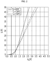
- an initial collector-emitter voltage V CEO and an initial collector-emitter resistance R CE which are parameters used in Equation 1 for calculating a conduction loss P C_IGBT , may be determined from a graph that is provided from the manufacturer as shown in FIG. 2 .
- FIG. 2 is a characteristic graph of an IGBT according to temperature, which is provided from a manufacturer
- FIG. 3 is an exemplary diagram for describing a process of determining a parameter in FIG. 2 .
- a value corresponding to a condition is obtained from a graph shown in FIG. 2 , or a slope value (resistance) and an x intercept ( V CEO ) configuring a first order function are obtained through a linearization as shown in FIG. 3 , thereby obtaining the parameter.
- the parameter used in the loss calculation is varied according to temperature. Therefore, the manufacturer provides a parameter based on three temperatures (for example, 25°C, 125°C, and 150°C).
- temperatures for example, 25°C, 125°C, and 150°C.
- parameters required for configuring a graph with respect to an appropriate temperature should be stored in a memory, and an equation linearized through a parameter suitable for a corresponding temperature should also be stored.
- an object of the present disclosure is to provide a parameter determining apparatus for estimating temperature of a switching element of an inverter, which is capable of formulating a parameter variation according to a temperature variation to reduce an amount of data to be stored in a memory and simplify a calculating process.
- a parameter determining apparatus of one embodiment of the present disclosure may include an inverter unit including a power semiconductor module configured with at least one or more switching elements, and a control unit configured to determine an initial collector-emitter voltage of each of the at least one or more switching elements and collector-emitter resistance of each thereof by linearizing a collector-emitter voltage of each of the at least one or more switching elements at a certain temperature.
- control unit may determine a region of a current specified to a first current and a second current at a reference current region, and determine a collector-emitter voltage (third and fourth voltages) of each of the at least one or more switching elements at the first current and the second current and a certain temperature using a collector-emitter voltage (first and second voltages) of each thereof with respect to the first current and the second current at each of predetermined first and second temperatures, thereby linearizing the collector-emitter voltage of each of the at least one or more switching elements at the certain temperature.
- control unit may determine a third voltage using that a ratio of a difference between a second temperature and a first temperature with respect to a difference between the certain temperature and the first temperature is the same as that of a difference between the second voltage and the first voltage with respect to a difference between the third voltage and the first voltage at the first current.
- control unit may determine a fourth voltage using that a ratio of a difference between a second temperature and a first temperature with respect to a difference between the certain temperature and the first temperature is the same as that of a difference between the second voltage and the first voltage with respect to a difference between the fourth voltage and the first voltage at the second current.
- control unit may perform the linearization using (a first current, a third voltage) and (a second current, a fourth voltage).
- a parameter determining method for estimating temperature of a switching element in an inverter including a power semiconductor module configured with the at least one or more switching elements may include linearizing a collector-emitter voltage of each of the at least one or more switching elements at a certain temperature, and determining an initial collector-emitter voltage of each of the at least one or more switching elements and collector-emitter resistance of each thereof.
- the linearizing may include determining a region of a current specified to a first current and a second current at a reference current region, determining a collector-emitter voltage (third and fourth voltages) of each of the at least one or more switching elements at the first current and the second current and a certain temperature using a collector-emitter voltage (first and second voltages) of each thereof with respect to the first current and the second current at each of predetermined first and second temperatures, and linearizing the collector-emitter voltage of each of the at least one or more switching elements at the certain temperature.
- the third voltage may be determined using that a ratio of a difference between a second temperature and a first temperature with respect to a difference between the certain temperature and the first temperature is the same as that of a difference between the second voltage and the first voltage with respect to a difference between the third voltage and the first voltage at the first current.
- the fourth voltage may be determined using that a ratio of a difference between a second temperature and a first temperature with respect to a difference between the certain temperature and the first temperature is the same as that of a difference between the second voltage and the first voltage with respect to a difference between the fourth voltage and the first voltage at the second current.
- the present disclosure provides an effect in which a memory storing capacity is reduced and a size of program is decreased by linearizing and simplifying a variation of a parameter according to temperature in an equation without storing a parameter in a memory to obtain an appropriate V CE , or performing a complicated calculation so as to obtain V CE .
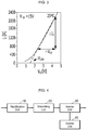
- FIG. 4 is a block diagram of a parameter determining apparatus for estimating temperature of a switching element of an inverter according to one embodiment of the present disclosure.
- FIG. 5 is a characteristic graph of an insulated gate bipolar transistor (IGBT) according to temperature, which is provided from a manufacturer.
- FIG. 6 is one exemplary diagram for describing a process of estimating a parameter in FIG. 5 according to one embodiment of the present disclosure.
- IGBT insulated gate bipolar transistor
- a parameter determining apparatus is to estimate temperature of a junction of a switching element configuring an inverter unit 30 in an inverter configured with a rectification unit 10, a smoothing unit 20 and the inverter unit 30, and may include a control unit 40.
- the inverter unit 30 may be configured to include a power semiconductor module, and the power semiconductor module may be configured with a plurality of switching elements arranged therein.
- the switching element will be exemplified and described as an IGBT, but the present disclosure is not limited thereto, and it will be apparent to those skilled in the art that a variety of semiconductor switching elements may be used according to a configuration of an inverter.
- the control unit 40 may be, for example, a microcontroller unit (MCU) provided inside the inverter, and may obtain a parameter at a practical temperature from a parameter provided from a manufacturer through a process which will be described below.
- MCU microcontroller unit
- the control unit 40 may select a current to be a reference from a parameter provided from a manufacturer as shown in FIG. 5 .
- a current region being selected may be varied according to a rated current of the inverter unit 30, and may be defined as a region specified by currents I A and I B in one embodiment of the present disclosure.
- a current range applied to the inverter unit 30 is a region between the currents I A and I B . If the current range is assumed to be linear, it may be expressed in the form of a first order function as shown in FIG. 6 .
- the graph of FIG. 5 which provided from the manufacturer, provides a parameter with respect to a limited temperature, for example, 25°C, 125°C, 150°C, respectively.
- a result of a linear approximation with respect to two temperatures is shown in FIG. 6 .
- a black solid line represents V CE according to a current variation at 25°C
- a black dotted line represents V CE according to a current variation at 150°C
- a blue solid line represents a linearization of V CE according to a current variation at 25°C
- a red solid line represents a linearization of V CE according to a current variation at 150°C
- a light green solid line represents a linearization of V CE according to a current variation at a certain temperature T K .
- V CE corresponding to 25°C and 150°C is V CE_A25 , V CE_A150 , V CE_B25 , and V CE_B150 , and V CE at a specific temperature is V CE_ATK and V CE_BTK , V CE is an intersecting point with respect to the reference current as shown in FIG. 5 .
- V CE_BTK may be calculated as the following Equation.
- V CE with respect to the current I A may be calculated as follows.
- V CE_ATK T K ⁇ 25 150 ⁇ 25 ⁇ V CE_A 150 ⁇ V CE_A 25 + V CE_A 25
- V CE at the reference currents I A and I B is V CE_ATK and V CE_BTK , respectively, at the temperature T K
- a straight line connecting V CE_ATK to V CE BTK is a first order function representing V CE according to a current at the temperature T K , so that it can be seen that the straight line is the light green graph in FIGS. 5 and 6 . Therefore, a linear equation is calculated from two points of ( I A , V CE_ATK ) and ( I B , V CE_BTK ) to be expressed as follows.
- V CE R CE TK I C + V CE 0 TK
- Equation 5 I C is a magnitude of a current that actually flows at the inverter unit 30. That is, when the current I C flows at the temperature T K , V CE may be calculated from Equation 5.
- R CE_TK and V CE0_TK of Equation 5 may be expressed as the following Equation.
- R CE_TK V CE_BTK ⁇ V CE_ ATK I B ⁇ I A
- V CE 0 TK V CE_BTK ⁇ R CE_ TK I B
- control unit 40 may determine V CE at the temperature T K when a current is I C from the parameter inputs of V CE_A25 , V CE_A150 , V CE_B25 , and V CE_B150 using Equations 3 to 6.
- a memory storing capacity may be reduced and a size of program may be decreased by linearizing and simplifying a variation of a parameter according to temperature in an equation without storing a parameter in a memory to obtain an appropriate V CE , or performing a complicated calculation so as to obtain V CE .
- FIG. 7 is a flow chart of one embodiment for describing a process of determining a parameter for estimating temperature of a switching element of an inverter in one embodiment of the present disclosure.
- the control unit 40 of one embodiment of the present disclosure calculates a loss based on a temperature of a point at which a temperature of the inverter unit 30 can be measured. Further, a temperature difference is calculated using the calculated loss and thermal resistance between the point at which the temperature is measured and a junction of the inverter 30, and a temperature of the junction is estimated using Equations 1 and 2.
- a region of a current applied to the inverter unit 30 may be determined in Operation S71. That is, I A and I B which are respectively upper and lower values of the region of the current may be determined from the graph of FIG. 5 representing a relationship between a current and a voltage and provided from a manufacturer. I A and I B may be determined according to a rated voltage of an inverter.
- control unit 40 may obtain V CE_A25 , V CE_A150 , V CE_B25 , and V CE_B150 which are V CE at a temperature (for example, 25°C and 150°C) determinable from a graph provided from a manufacturer, which is with respect to currents I A and I B in Operation S72.
- intersecting points V CE_ATK and V CE_BTK corresponding to the currents I A and I B at the certain temperature T K may be determined using Equations 3 and 4 in Operation S73, and a linear equation corresponding to V CE at the certain temperature T K may be calculated from two points ( I A , V CE_ATK ) and ( I B , V CE_BTK ) as in Equation 5 in Operation S74.
- control unit 40 may determine parameters R CE_TK and V CE0_TK for estimating a temperature of a junction of a switching element of the inverter unit 30 at the certain temperature T K using Equation 6 in Equation S75.
- Equation 1 a conduction loss of Equation 1 may be calculated using the parameters R CE_TK and V CE0_TK determined by the control unit 40 (not shown).
- the conduction loss determined as described above is added to a switching loss determined using a separate parameter, and the added result is multiplied by thermal resistance provided from the manufacturer, and then a temperature difference between a junction of a switching element and a point at which a temperature of a power semiconductor module of the inverter unit 30 is possible is calculated and the temperature difference is added to the measured reference temperature, so that the temperature of the junction of the switching element may be estimated.
- a parameter variation according to a variation of temperature is mathematized as a first order function so that a parameter in which a variation according to temperature is corrected using a simplified equation may be calculated.
- Rectification Unit 20 Smoothing Unit 30: Inverter Unit 40: Control Unit
Landscapes
- Physics & Mathematics (AREA)
- General Physics & Mathematics (AREA)
- Engineering & Computer Science (AREA)
- Power Engineering (AREA)
- Microelectronics & Electronic Packaging (AREA)
- Inverter Devices (AREA)
- Power Conversion In General (AREA)
Abstract
Description
- The present disclosure relates to a parameter determining apparatus for estimating temperature of a switching element of an inverter.
- Generally, a multi-purpose inverter is configured with a rectification unit, a direct current (DC) link capacitor, and an inverter unit, and the inverter unit is configured with a power semiconductor module. Such a power semiconductor module turns on and off a current while an inverter operates such that heat is generated.
- When temperature of the power semiconductor module rises over a predetermined temperature, a switching element configuring the power semiconductor module is damaged so that a temperature rising is a major consideration factor in selecting the power semiconductor module.
-
FIG. 1 is a cross sectional view for describing a configuration of a conventional power semiconductor module. - A
power semiconductor module 200 is arranged on a printed circuit board (PCB) 100, and aheatsink 300 is arranged below thePCB 100 to radiate heat generated from thepower semiconductor module 200. A plurality ofswitching elements 220 of a chip shape are arranged on aninner substrate 210 inside thepower semiconductor module 200. Each of theswitching elements 220 is, for example, an insulated gate bipolar transistor (IGBT). In such a configuredpower semiconductor module 200, a heating point of highest temperature is a junction A inside theswitching element 220, but the junction A is located inside thepower semiconductor module 200 so that temperature could not be directly measured. Therefore, the temperature of the junction A of theswitching element 220 is indirectly estimated and a margin is added to the estimated temperature, thereby preventing a temperature rising of the junction A. - A method for indirectly estimating temperature of the junction A is to calculate a loss based on temperature of a position (for example, B of
FIG. 1 ) at which a temperature measurement may be possible. Then, a temperature difference is calculated using the calculated loss and a thermal resistance between the position at which the temperature is measured and the junction of theswitching element 220, thereby estimating temperature of a junction. When the loss is calculated during such a process, an intrinsic parameter of theswitching element 220 is used and this intrinsic parameter is experimentally provided by each of manufacturers. That is, the loss is estimated using a parameter under a specific condition among parameters varied according to a temperature variation. - To estimate temperature of a junction of a switching element, a process of calculating a loss of the
switching element 220 is as follows. It will be described a case in which theswitching element 220 is an IGBT. - In other words, a temperature difference is calculated by adding a conduction loss and a switching loss of the
switching element 220 to a conduction loss and a switching loss of an anti-parallel diode of the IGBT and by multiplying the added result by thermal resistance provided from a manufacturer, and then a temperature difference from a measured reference temperature is added to the calculated temperature difference to estimate temperature of a junction of the IGBT. At this point, the following Equations are used.

- In
Equations power semiconductor module 200, which are provided from a manufacturer. At this point, an initial collector-emitter voltage VCEO and an initial collector-emitter resistance RCE, which are parameters used inEquation 1 for calculating a conduction loss PC_IGBT , may be determined from a graph that is provided from the manufacturer as shown inFIG. 2 . -
FIG. 2 is a characteristic graph of an IGBT according to temperature, which is provided from a manufacturer, andFIG. 3 is an exemplary diagram for describing a process of determining a parameter inFIG. 2 . - Because a parameter used in calculation of a conduction loss is nonlinear, a value corresponding to a condition is obtained from a graph shown in
FIG. 2 , or a slope value (resistance) and an x intercept (VCEO ) configuring a first order function are obtained through a linearization as shown inFIG. 3 , thereby obtaining the parameter. - As shown in
FIG. 2 , the parameter used in the loss calculation is varied according to temperature. Therefore, the manufacturer provides a parameter based on three temperatures (for example, 25°C, 125°C, and 150°C). When the parameter is directly obtained from a graph, an appropriate point may be determined according to temperature, whereas, when the parameter is obtained through a processor, all information with respect to the parameter should be provided so as to obtain an appropriate value. - Also, even when
FIG. 3 is used, parameters required for configuring a graph with respect to an appropriate temperature should be stored in a memory, and an equation linearized through a parameter suitable for a corresponding temperature should also be stored. - Consequently, there are problems in that an amount of data to be stored in a memory is increased so as to consider temperature variation and a calculation process of the data is complicated.
- To address the problems described above, an object of the present disclosure is to provide a parameter determining apparatus for estimating temperature of a switching element of an inverter, which is capable of formulating a parameter variation according to a temperature variation to reduce an amount of data to be stored in a memory and simplify a calculating process.
- To attain the object of the present disclosure, a parameter determining apparatus of one embodiment of the present disclosure may include an inverter unit including a power semiconductor module configured with at least one or more switching elements, and a control unit configured to determine an initial collector-emitter voltage of each of the at least one or more switching elements and collector-emitter resistance of each thereof by linearizing a collector-emitter voltage of each of the at least one or more switching elements at a certain temperature.
- In one embodiment of the present disclosure, the control unit may determine a region of a current specified to a first current and a second current at a reference current region, and determine a collector-emitter voltage (third and fourth voltages) of each of the at least one or more switching elements at the first current and the second current and a certain temperature using a collector-emitter voltage (first and second voltages) of each thereof with respect to the first current and the second current at each of predetermined first and second temperatures, thereby linearizing the collector-emitter voltage of each of the at least one or more switching elements at the certain temperature.
- In one embodiment of the present disclosure, the control unit may determine a third voltage using that a ratio of a difference between a second temperature and a first temperature with respect to a difference between the certain temperature and the first temperature is the same as that of a difference between the second voltage and the first voltage with respect to a difference between the third voltage and the first voltage at the first current.
- In one embodiment of the present disclosure, the control unit may determine a fourth voltage using that a ratio of a difference between a second temperature and a first temperature with respect to a difference between the certain temperature and the first temperature is the same as that of a difference between the second voltage and the first voltage with respect to a difference between the fourth voltage and the first voltage at the second current.
- In one embodiment of the present disclosure, the control unit may perform the linearization using (a first current, a third voltage) and (a second current, a fourth voltage).
- Also, to attain the object of the present disclosure, a parameter determining method for estimating temperature of a switching element in an inverter including a power semiconductor module configured with the at least one or more switching elements according to one embodiment of the present disclosure may include linearizing a collector-emitter voltage of each of the at least one or more switching elements at a certain temperature, and determining an initial collector-emitter voltage of each of the at least one or more switching elements and collector-emitter resistance of each thereof.
- In one embodiment of the present disclosure, the linearizing may include determining a region of a current specified to a first current and a second current at a reference current region, determining a collector-emitter voltage (third and fourth voltages) of each of the at least one or more switching elements at the first current and the second current and a certain temperature using a collector-emitter voltage (first and second voltages) of each thereof with respect to the first current and the second current at each of predetermined first and second temperatures, and linearizing the collector-emitter voltage of each of the at least one or more switching elements at the certain temperature.
- In one embodiment of the present disclosure, the third voltage may be determined using that a ratio of a difference between a second temperature and a first temperature with respect to a difference between the certain temperature and the first temperature is the same as that of a difference between the second voltage and the first voltage with respect to a difference between the third voltage and the first voltage at the first current.
- In one embodiment of the present disclosure, the fourth voltage may be determined using that a ratio of a difference between a second temperature and a first temperature with respect to a difference between the certain temperature and the first temperature is the same as that of a difference between the second voltage and the first voltage with respect to a difference between the fourth voltage and the first voltage at the second current.
- As described above, the present disclosure provides an effect in which a memory storing capacity is reduced and a size of program is decreased by linearizing and simplifying a variation of a parameter according to temperature in an equation without storing a parameter in a memory to obtain an appropriate VCE , or performing a complicated calculation so as to obtain VCE .
- Also, in accordance with the present disclosure, there is an effect in which a parameter variation according to a variation of temperature is mathematized as a first order function so that a parameter in which a variation according to temperature is corrected using a simplified equation may be calculated.
-
-
FIG. 1 is a cross sectional view for describing a configuration of a conventional power semiconductor module. -
FIG. 2 is a characteristic graph of an insulated gate bipolar transistor (IGBT) according to temperature, which is provided from a manufacturer. -
FIG. 3 is an exemplary diagram for describing a process of determining a parameter inFIG. 2 . -
FIG. 4 is a block diagram of a parameter determining apparatus for estimating temperature of a switching element of an inverter according to one embodiment of the present disclosure. -
FIG. 5 is a characteristic graph of an IGBT according to temperature, which is provided from a manufacturer. -
FIG. 6 is one exemplary diagram for describing a process of estimating a parameter inFIG. 5 according to one embodiment of the present disclosure. -
FIG. 7 is a flow chart of one embodiment for describing a process of determining a parameter for estimating temperature of a switching element of an inverter in one embodiment of the present disclosure. - The present disclosure may be variously modified and will have a variety of embodiments so that specific embodiments will be exemplified in the drawings and will be described in detail. The specific embodiments disclosed herein, however, are not to be taken in a sense for limiting the present disclosure to these embodiments, but for explanation thereof and it should be understood that numerous other alternations, equivalents and substituents will be falling within the spirit and scope of the present disclosure.
- Hereinafter, one preferred embodiment according to the present disclosure will be described in detail with reference to the accompanying drawings.
-
FIG. 4 is a block diagram of a parameter determining apparatus for estimating temperature of a switching element of an inverter according to one embodiment of the present disclosure.FIG. 5 is a characteristic graph of an insulated gate bipolar transistor (IGBT) according to temperature, which is provided from a manufacturer. Further,FIG. 6 is one exemplary diagram for describing a process of estimating a parameter inFIG. 5 according to one embodiment of the present disclosure. - A parameter determining apparatus according to the present disclosure is to estimate temperature of a junction of a switching element configuring an
inverter unit 30 in an inverter configured with arectification unit 10, asmoothing unit 20 and theinverter unit 30, and may include acontrol unit 40. - As shown in
FIG. 1 , theinverter unit 30 may be configured to include a power semiconductor module, and the power semiconductor module may be configured with a plurality of switching elements arranged therein. In one embodiment of the present disclosure, the switching element will be exemplified and described as an IGBT, but the present disclosure is not limited thereto, and it will be apparent to those skilled in the art that a variety of semiconductor switching elements may be used according to a configuration of an inverter. - The
control unit 40 may be, for example, a microcontroller unit (MCU) provided inside the inverter, and may obtain a parameter at a practical temperature from a parameter provided from a manufacturer through a process which will be described below. - The
control unit 40 according to one embodiment of the present disclosure may select a current to be a reference from a parameter provided from a manufacturer as shown inFIG. 5 . At this point, a current region being selected may be varied according to a rated current of theinverter unit 30, and may be defined as a region specified by currents IA and IB in one embodiment of the present disclosure. - A current range applied to the
inverter unit 30 is a region between the currents IA and IB. If the current range is assumed to be linear, it may be expressed in the form of a first order function as shown inFIG. 6 . - The graph of
FIG. 5 , which provided from the manufacturer, provides a parameter with respect to a limited temperature, for example, 25°C, 125°C, 150°C, respectively. Here, a result of a linear approximation with respect to two temperatures (25°C and 150°C in one embodiment of the present disclosure) is shown inFIG. 6 . - In
FIGS. 5 and6 , a black solid line represents VCE according to a current variation at 25°C, a black dotted line represents VCE according to a current variation at 150°C, a blue solid line represents a linearization of VCE according to a current variation at 25°C, a red solid line represents a linearization of VCE according to a current variation at 150°C, and a light green solid line represents a linearization of VCE according to a current variation at a certain temperature TK. - The result of the parameter and the result of the linear approximation, each of which corresponds to each temperature, show similar to each other except when a current is very small, as can be seen from
FIG. 5 . As shown inFIGS. 5 and6 , in one embodiment of the present disclosure, it is assumed that generation of a parameter variation according to a temperature variation is a first order linear function. - When a reference current IC is IA and IB, VCE corresponding to 25°C and 150°C is VCE_A25 , VCE_A150 , VCE_B25 , and VCE_B150 , and VCE at a specific temperature is VCE_ATK and VCE_BTK, VCE is an intersecting point with respect to the reference current as shown in
FIG. 5 . InFIGS. 5 and6 , if a variation of the parameter is assumed to be linear with respect to temperature, VCE_BTK may be calculated as the following Equation.
- Similarly, when a temperature is TK, VCE with respect to the current IA may be calculated as follows.

- VCE at the reference currents IA and IB is VCE_ATK and VCE_BTK , respectively, at the temperature TK, and a straight line connecting VCE_ATK to VCE BTK is a first order function representing VCE according to a current at the temperature TK , so that it can be seen that the straight line is the light green graph in
FIGS. 5 and6 . Therefore, a linear equation is calculated from two points of (IA , VCE_ATK ) and (IB , VCE_BTK ) to be expressed as follows.
- In
Equation 5, IC is a magnitude of a current that actually flows at theinverter unit 30. That is, when the current IC flows at the temperature TK, VCE may be calculated fromEquation 5. RCE_TK and VCE0_TK ofEquation 5 may be expressed as the following Equation.
- Therefore, the
control unit 40 may determine VCE at the temperature TK when a current is IC from the parameter inputs of VCE_A25 , VCE_A150 , VCE_B25 , and VCE_B150 using Equations 3 to 6. - As described above, in accordance with one embodiment of the present disclosure, a memory storing capacity may be reduced and a size of program may be decreased by linearizing and simplifying a variation of a parameter according to temperature in an equation without storing a parameter in a memory to obtain an appropriate VCE, or performing a complicated calculation so as to obtain VCE .
-
FIG. 7 is a flow chart of one embodiment for describing a process of determining a parameter for estimating temperature of a switching element of an inverter in one embodiment of the present disclosure. - As shown in
FIG. 7 , thecontrol unit 40 of one embodiment of the present disclosure calculates a loss based on a temperature of a point at which a temperature of theinverter unit 30 can be measured. Further, a temperature difference is calculated using the calculated loss and thermal resistance between the point at which the temperature is measured and a junction of theinverter 30, and a temperature of the junction is estimated usingEquations - At this point, in order to determine an initial collector-emitter voltage VCEO of a switching element and a collector-emitter resistance RCE thereof, which are parameters at a certain temperature, a region of a current applied to the
inverter unit 30 may be determined in Operation S71. That is, IA and IB which are respectively upper and lower values of the region of the current may be determined from the graph ofFIG. 5 representing a relationship between a current and a voltage and provided from a manufacturer. IA and IB may be determined according to a rated voltage of an inverter. - With such an operation, the
control unit 40 may obtain VCE_A25, VCE_A150 , VCE_B25 , and VCE_B150 which are VCE at a temperature (for example, 25°C and 150°C) determinable from a graph provided from a manufacturer, which is with respect to currents IA and IB in Operation S72. - Thereafter, intersecting points VCE_ATK and VCE_BTK corresponding to the currents IA and IB at the certain temperature TK may be determined using
Equations Equation 5 in Operation S74. - Afterward, the
control unit 40 may determine parameters RCE_TK and VCE0_TK for estimating a temperature of a junction of a switching element of theinverter unit 30 at the certain temperature TK using Equation 6 in Equation S75. - Therefore, a conduction loss of
Equation 1 may be calculated using the parameters RCE_TK and VCE0_TK determined by the control unit 40 (not shown). - The conduction loss determined as described above is added to a switching loss determined using a separate parameter, and the added result is multiplied by thermal resistance provided from the manufacturer, and then a temperature difference between a junction of a switching element and a point at which a temperature of a power semiconductor module of the
inverter unit 30 is possible is calculated and the temperature difference is added to the measured reference temperature, so that the temperature of the junction of the switching element may be estimated. - In accordance with the present disclosure, a parameter variation according to a variation of temperature is mathematized as a first order function so that a parameter in which a variation according to temperature is corrected using a simplified equation may be calculated.
- The present disclosure has been described with reference to the embodiments shown in the drawings, but is merely an illustration, and it should be understood that numerous other modifications and equivalent other embodiments can be devised by those skilled in the art. Therefore, the technical scope of the present invention should be defined by the appended claims.
-
10: Rectification Unit 20: Smoothing Unit 30: Inverter Unit 40: Control Unit
Claims (9)
- A parameter determining apparatus, comprising:an inverter unit (30) including a power semiconductor module configured with at least one or more switching elements; anda control unit (40) configured to determine an initial collector-emitter voltage of each of the at least one or more switching elements and collector-emitter resistance of each thereof by linearizing a collector-emitter voltage of each of the at least one or more switching elements at a certain temperature.
- The parameter determining apparatus of claim 1, wherein the control unit determines a region of a current specified to a first current and a second current at a reference current region, and determines a collector-emitter voltage (third and fourth voltages) of each of the at least one or more switching elements at the first current and the second current and a certain temperature using a collector-emitter voltage (first and second voltages) of each thereof with respect to the first current and the second current at each of predetermined first and second temperatures, thereby linearizing the collector-emitter voltage of each of the at least one or more switching elements at the certain temperature.
- The parameter determining apparatus of claim 2, wherein the control unit determines a third voltage using that a ratio of a difference between a second temperature and a first temperature with respect to a difference between the certain temperature and the first temperature is the same as that of a difference between the second voltage and the first voltage with respect to a difference between the third voltage and the first voltage at the first current.
- The parameter determining apparatus of claim 2, wherein the control unit determines a fourth voltage using that a ratio of a difference between a second temperature and a first temperature with respect to a difference between the certain temperature and the first temperature is the same as that of a difference between the second voltage and the first voltage with respect to a difference between the fourth voltage and the first voltage at the second current.
- The parameter determining apparatus of claim 1, wherein the control unit performs the linearization using two points of (a first current, a third voltage) and (a second current, a fourth voltage).
- A parameter determining method for estimating temperature of a switching element in an inverter including a power semiconductor module configured with the at least one or more switching elements, comprising:linearizing a collector-emitter voltage of each of the at least one or more switching elements at a certain temperature; anddetermining an initial collector-emitter voltage of each of the at least one or more switching elements and collector-emitter resistance of each thereof.
- The parameter determining method of claim 6, wherein the linearizing includes:determining a region of a current specified to a first current and a second current at a reference current region;determining a collector-emitter voltage (third and fourth voltages) of each of the at least one or more switching elements at the first current and the second current and a certain temperature using a collector-emitter voltage (first and second voltages) of each thereof with respect to the first current and the second current at each of predetermined first and second temperatures; andlinearizing the collector-emitter voltage of each of the at least one or more switching elements at the certain temperature.
- The parameter determining method of claim 7, wherein the third voltage is determined using that a ratio of a difference between a second temperature and a first temperature with respect to a difference between the certain temperature and the first temperature is the same as that of a difference between the second voltage and the first voltage with respect to a difference between the third voltage and the first voltage at the first current.
- The parameter determining method of claim 7, wherein the fourth voltage is determined using that a ratio of a difference between a second temperature and a first temperature with respect to a difference between the certain temperature and the first temperature is the same as that of a difference between the second voltage and the first voltage with respect to a difference between the fourth voltage and the first voltage at the second current.
Applications Claiming Priority (1)
| Application Number | Priority Date | Filing Date | Title |
|---|---|---|---|
| KR1020160047620A KR102469942B1 (en) | 2016-04-19 | 2016-04-19 | Apparatus for determining parameter when estimating temperature of switching element in inverter |
Publications (2)
| Publication Number | Publication Date |
|---|---|
| EP3236223A1 true EP3236223A1 (en) | 2017-10-25 |
| EP3236223B1 EP3236223B1 (en) | 2021-01-27 |
Family
ID=57777366
Family Applications (1)
| Application Number | Title | Priority Date | Filing Date |
|---|---|---|---|
| EP16201178.7A Active EP3236223B1 (en) | 2016-04-19 | 2016-11-29 | Parameter determining apparatus for estimating temperature of switching element of inverter |
Country Status (6)
| Country | Link |
|---|---|
| US (1) | US10466114B2 (en) |
| EP (1) | EP3236223B1 (en) |
| JP (1) | JP6266081B2 (en) |
| KR (1) | KR102469942B1 (en) |
| CN (1) | CN107305146B (en) |
| ES (1) | ES2862305T3 (en) |
Families Citing this family (4)
| Publication number | Priority date | Publication date | Assignee | Title |
|---|---|---|---|---|
| EP3627121B1 (en) * | 2018-09-21 | 2022-07-06 | Maschinenfabrik Reinhausen GmbH | Determining a characteristic temperature of an electric or electronic system |
| DE102019101163B3 (en) * | 2019-01-17 | 2020-06-04 | Schaeffler Technologies AG & Co. KG | Electric drive unit and method for temperature calculation in an electric drive unit |
| JP7472663B2 (en) | 2020-06-05 | 2024-04-23 | 富士電機株式会社 | Power Conversion Equipment |
| KR102813894B1 (en) * | 2024-12-11 | 2025-05-29 | 한국전자기술연구원 | Power conversion device with multi-phase interleaving structure |
Citations (3)
| Publication number | Priority date | Publication date | Assignee | Title |
|---|---|---|---|---|
| EP2568268A1 (en) * | 2011-09-07 | 2013-03-13 | kk-electronic a/s | Method for estimating the temperature of a semiconductor chip |
| WO2015044205A1 (en) * | 2013-09-24 | 2015-04-02 | Abb Technology Ag | Method and apparatus for determining an actual junction temperature of an igbt device |
| US20150211938A1 (en) * | 2012-12-12 | 2015-07-30 | Fuji Electric Co., Ltd. | Semiconductor chip temperature estimation device and overheat protection device |
Family Cites Families (27)
| Publication number | Priority date | Publication date | Assignee | Title |
|---|---|---|---|---|
| US5237481A (en) * | 1991-05-29 | 1993-08-17 | Ixys Corporation | Temperature sensing device for use in a power transistor |
| JP3194353B2 (en) * | 1996-07-26 | 2001-07-30 | トヨタ自動車株式会社 | Semiconductor module temperature detector |
| JP2004045305A (en) * | 2002-07-15 | 2004-02-12 | Mitsubishi Electric Corp | Overcurrent detection circuit |
| DE102005036317B4 (en) * | 2005-07-29 | 2010-02-11 | Aloys Wobben | Method and device for determining the power loss of an electronic switch, inverter, wind turbine with methods of control |
| FR2901634B1 (en) * | 2006-05-23 | 2008-08-29 | Converteam Sas | METHOD AND DEVICE FOR MEASURING THE JUNCTION TEMPERATURE OF AN ELECTRONIC COMPONENT. |
| JP2010139273A (en) | 2008-12-09 | 2010-06-24 | Nissan Motor Co Ltd | Method and device for testing semiconductor element |
| KR101541706B1 (en) | 2009-01-19 | 2015-08-05 | 삼성전자주식회사 | Temperature sensing oscillator circuit and semiconductor memory device including the same |
| JP2011125101A (en) | 2009-12-09 | 2011-06-23 | Furukawa Electric Co Ltd:The | Current detector, power supply device and current detection method |
| KR101103425B1 (en) * | 2010-11-22 | 2012-01-09 | 영남대학교 산학협력단 | Capacity Estimation Method and System Using Temperature Compensation of Electrolytic Capacitor for PPM Converter |
| KR101327647B1 (en) * | 2012-03-29 | 2013-11-12 | 엘에스산전 주식회사 | Apparatus for diagnosing dc link capacitor of inverter |
| JP2014050307A (en) | 2012-09-04 | 2014-03-17 | Ricoh Co Ltd | Slope compensation circuit and method, and switching regulator |
| US9335223B2 (en) * | 2012-09-05 | 2016-05-10 | Texas Instruments Incorporated | Circuits and methods for determining the temperature of a transistor |
| KR20140064322A (en) | 2012-11-20 | 2014-05-28 | 삼성전기주식회사 | Apparatus for measuring temperature of power semiconductor device and module |
| US9595889B2 (en) * | 2013-02-15 | 2017-03-14 | Eaton Corporation | System and method for single-phase and three-phase current determination in power converters and inverters |
| US9240775B2 (en) * | 2013-03-12 | 2016-01-19 | Intel Deutschland Gmbh | Circuit arrangements |
| JP6102452B2 (en) * | 2013-04-17 | 2017-03-29 | 富士電機株式会社 | Manufacturing method of semiconductor device and weight for soldering |
| CN203572583U (en) * | 2013-09-18 | 2014-04-30 | 深圳市绿恩环保技术有限公司 | Temperature transforming circuit and temperature transformer |
| JP6511220B2 (en) | 2013-12-19 | 2019-05-15 | 高周波熱錬株式会社 | Power converter and method |
| US9575113B2 (en) * | 2014-02-07 | 2017-02-21 | Infineon Technologies Ag | Insulated-gate bipolar transistor collector-emitter saturation voltage measurement |
| JP2015153185A (en) * | 2014-02-14 | 2015-08-24 | 国立大学法人広島大学 | Power switching device simulation method |
| KR101443854B1 (en) * | 2014-02-27 | 2014-09-23 | 연세대학교 산학협력단 | Modeling structure for switching device and method for electromagnetic transients program simulation using it |
| EP2933646B1 (en) * | 2014-04-17 | 2019-04-17 | Siemens Aktiengesellschaft | Precision measurement of voltage drop across a semiconductor switching element |
| CN103997108B (en) * | 2014-04-18 | 2017-09-01 | 河南速达电动汽车科技有限公司 | Charger for lead-acid battery of electric vehicle |
| JP6180372B2 (en) * | 2014-06-06 | 2017-08-16 | 三菱電機株式会社 | Semiconductor element inspection method and inspection apparatus |
| JP6165683B2 (en) | 2014-07-02 | 2017-07-19 | 日立オートモティブシステムズ株式会社 | Inverter device |
| KR101567256B1 (en) * | 2014-11-06 | 2015-11-13 | 현대자동차주식회사 | Apparatus and method for predicting junction temperature for inverter |
| CN204464960U (en) * | 2015-03-18 | 2015-07-08 | 吴英明 | A motor temperature protection device |
-
2016
- 2016-04-19 KR KR1020160047620A patent/KR102469942B1/en active Active
- 2016-11-29 CN CN201611073781.2A patent/CN107305146B/en active Active
- 2016-11-29 ES ES16201178T patent/ES2862305T3/en active Active
- 2016-11-29 US US15/363,553 patent/US10466114B2/en active Active
- 2016-11-29 EP EP16201178.7A patent/EP3236223B1/en active Active
- 2016-12-02 JP JP2016235324A patent/JP6266081B2/en not_active Expired - Fee Related
Patent Citations (3)
| Publication number | Priority date | Publication date | Assignee | Title |
|---|---|---|---|---|
| EP2568268A1 (en) * | 2011-09-07 | 2013-03-13 | kk-electronic a/s | Method for estimating the temperature of a semiconductor chip |
| US20150211938A1 (en) * | 2012-12-12 | 2015-07-30 | Fuji Electric Co., Ltd. | Semiconductor chip temperature estimation device and overheat protection device |
| WO2015044205A1 (en) * | 2013-09-24 | 2015-04-02 | Abb Technology Ag | Method and apparatus for determining an actual junction temperature of an igbt device |
Also Published As
| Publication number | Publication date |
|---|---|
| CN107305146B (en) | 2020-09-01 |
| KR20170119507A (en) | 2017-10-27 |
| JP2017195758A (en) | 2017-10-26 |
| EP3236223B1 (en) | 2021-01-27 |
| US20170299443A1 (en) | 2017-10-19 |
| US10466114B2 (en) | 2019-11-05 |
| CN107305146A (en) | 2017-10-31 |
| ES2862305T3 (en) | 2021-10-07 |
| KR102469942B1 (en) | 2022-11-22 |
| JP6266081B2 (en) | 2018-01-24 |
Similar Documents
| Publication | Publication Date | Title |
|---|---|---|
| US20190204889A1 (en) | Power conversion device and semiconductor device | |
| KR102388147B1 (en) | IGBT temperature sensor correction device and temperature sensing correction method using the same | |
| US10466114B2 (en) | Parameter determining apparatus for estimating temperature of switching element of inverter | |
| US9016939B2 (en) | Thermal sensor with second-order temperature curvature correction | |
| US20160377488A1 (en) | Temperature estimation in power semiconductor device in electric drvie system | |
| JP6878802B2 (en) | Semiconductor devices and their driving methods | |
| CN110994549B (en) | Over-temperature protection method and circuit for power switch | |
| WO2017119126A1 (en) | Semiconductor device | |
| CN111505475B (en) | Method and device for calibrating parameters of electric heating model of power semiconductor module | |
| JP5904136B2 (en) | Detection temperature error correction method and detection temperature error correction system | |
| JP2007093335A (en) | Method and device for measuring temperature of semiconductor device | |
| US20160033339A1 (en) | Power device temperature monitor | |
| EP4166953B1 (en) | Method and apparatus for detecting insulation impedance of photovoltaic inverter | |
| Górecki | Investigation of the influence of thermal phenomena on characteristics of IGBTs contained in power modules | |
| JP2023023918A (en) | Method for manufacturing semiconductor device | |
| JP2014025867A (en) | Temperature sensing device | |
| CN115291590B (en) | Online evaluation method, device, motor controller and medium for output current limitation | |
| CN118671653A (en) | A power module fault warning method, device, equipment and medium | |
| EP2401812B1 (en) | Method and apparatus for maintaining circuit stability | |
| KR20050107852A (en) | A temperature estimate system and method of semiconductor power device | |
| KR20160104134A (en) | Method for controlling trip of inverter | |
| CN116457949A (en) | Power conversion device and control method for power conversion device | |
| WO2024232029A1 (en) | Power conversion apparatus and motor drive system | |
| CN118947056A (en) | Power conversion device, estimation program, and estimation method | |
| CN117991020A (en) | Inverter dead zone compensation time calibration method, device and medium, electronic equipment |
Legal Events
| Date | Code | Title | Description |
|---|---|---|---|
| PUAI | Public reference made under article 153(3) epc to a published international application that has entered the european phase |
Free format text: ORIGINAL CODE: 0009012 |
|
| STAA | Information on the status of an ep patent application or granted ep patent |
Free format text: STATUS: THE APPLICATION HAS BEEN PUBLISHED |
|
| AK | Designated contracting states |
Kind code of ref document: A1 Designated state(s): AL AT BE BG CH CY CZ DE DK EE ES FI FR GB GR HR HU IE IS IT LI LT LU LV MC MK MT NL NO PL PT RO RS SE SI SK SM TR |
|
| AX | Request for extension of the european patent |
Extension state: BA ME |
|
| STAA | Information on the status of an ep patent application or granted ep patent |
Free format text: STATUS: REQUEST FOR EXAMINATION WAS MADE |
|
| 17P | Request for examination filed |
Effective date: 20180425 |
|
| RBV | Designated contracting states (corrected) |
Designated state(s): AL AT BE BG CH CY CZ DE DK EE ES FI FR GB GR HR HU IE IS IT LI LT LU LV MC MK MT NL NO PL PT RO RS SE SI SK SM TR |
|
| STAA | Information on the status of an ep patent application or granted ep patent |
Free format text: STATUS: EXAMINATION IS IN PROGRESS |
|
| 17Q | First examination report despatched |
Effective date: 20181130 |
|
| GRAP | Despatch of communication of intention to grant a patent |
Free format text: ORIGINAL CODE: EPIDOSNIGR1 |
|
| STAA | Information on the status of an ep patent application or granted ep patent |
Free format text: STATUS: GRANT OF PATENT IS INTENDED |
|
| INTG | Intention to grant announced |
Effective date: 20201028 |
|
| RIN1 | Information on inventor provided before grant (corrected) |
Inventor name: YANG, JIN-KYU |
|
| GRAS | Grant fee paid |
Free format text: ORIGINAL CODE: EPIDOSNIGR3 |
|
| GRAA | (expected) grant |
Free format text: ORIGINAL CODE: 0009210 |
|
| STAA | Information on the status of an ep patent application or granted ep patent |
Free format text: STATUS: THE PATENT HAS BEEN GRANTED |
|
| AK | Designated contracting states |
Kind code of ref document: B1 Designated state(s): AL AT BE BG CH CY CZ DE DK EE ES FI FR GB GR HR HU IE IS IT LI LT LU LV MC MK MT NL NO PL PT RO RS SE SI SK SM TR |
|
| REG | Reference to a national code |
Ref country code: GB Ref legal event code: FG4D |
|
| REG | Reference to a national code |
Ref country code: CH Ref legal event code: EP |
|
| REG | Reference to a national code |
Ref country code: AT Ref legal event code: REF Ref document number: 1358794 Country of ref document: AT Kind code of ref document: T Effective date: 20210215 |
|
| REG | Reference to a national code |
Ref country code: IE Ref legal event code: FG4D |
|
| REG | Reference to a national code |
Ref country code: DE Ref legal event code: R096 Ref document number: 602016051998 Country of ref document: DE |
|
| REG | Reference to a national code |
Ref country code: NL Ref legal event code: MP Effective date: 20210127 |
|
| REG | Reference to a national code |
Ref country code: LT Ref legal event code: MG9D |
|
| REG | Reference to a national code |
Ref country code: AT Ref legal event code: MK05 Ref document number: 1358794 Country of ref document: AT Kind code of ref document: T Effective date: 20210127 |
|
| PG25 | Lapsed in a contracting state [announced via postgrant information from national office to epo] |
Ref country code: PT Free format text: LAPSE BECAUSE OF FAILURE TO SUBMIT A TRANSLATION OF THE DESCRIPTION OR TO PAY THE FEE WITHIN THE PRESCRIBED TIME-LIMIT Effective date: 20210527 Ref country code: NO Free format text: LAPSE BECAUSE OF FAILURE TO SUBMIT A TRANSLATION OF THE DESCRIPTION OR TO PAY THE FEE WITHIN THE PRESCRIBED TIME-LIMIT Effective date: 20210427 Ref country code: HR Free format text: LAPSE BECAUSE OF FAILURE TO SUBMIT A TRANSLATION OF THE DESCRIPTION OR TO PAY THE FEE WITHIN THE PRESCRIBED TIME-LIMIT Effective date: 20210127 Ref country code: FI Free format text: LAPSE BECAUSE OF FAILURE TO SUBMIT A TRANSLATION OF THE DESCRIPTION OR TO PAY THE FEE WITHIN THE PRESCRIBED TIME-LIMIT Effective date: 20210127 Ref country code: GR Free format text: LAPSE BECAUSE OF FAILURE TO SUBMIT A TRANSLATION OF THE DESCRIPTION OR TO PAY THE FEE WITHIN THE PRESCRIBED TIME-LIMIT Effective date: 20210428 Ref country code: BG Free format text: LAPSE BECAUSE OF FAILURE TO SUBMIT A TRANSLATION OF THE DESCRIPTION OR TO PAY THE FEE WITHIN THE PRESCRIBED TIME-LIMIT Effective date: 20210427 Ref country code: LT Free format text: LAPSE BECAUSE OF FAILURE TO SUBMIT A TRANSLATION OF THE DESCRIPTION OR TO PAY THE FEE WITHIN THE PRESCRIBED TIME-LIMIT Effective date: 20210127 |
|
| PG25 | Lapsed in a contracting state [announced via postgrant information from national office to epo] |
Ref country code: SE Free format text: LAPSE BECAUSE OF FAILURE TO SUBMIT A TRANSLATION OF THE DESCRIPTION OR TO PAY THE FEE WITHIN THE PRESCRIBED TIME-LIMIT Effective date: 20210127 Ref country code: AT Free format text: LAPSE BECAUSE OF FAILURE TO SUBMIT A TRANSLATION OF THE DESCRIPTION OR TO PAY THE FEE WITHIN THE PRESCRIBED TIME-LIMIT Effective date: 20210127 Ref country code: LV Free format text: LAPSE BECAUSE OF FAILURE TO SUBMIT A TRANSLATION OF THE DESCRIPTION OR TO PAY THE FEE WITHIN THE PRESCRIBED TIME-LIMIT Effective date: 20210127 Ref country code: PL Free format text: LAPSE BECAUSE OF FAILURE TO SUBMIT A TRANSLATION OF THE DESCRIPTION OR TO PAY THE FEE WITHIN THE PRESCRIBED TIME-LIMIT Effective date: 20210127 Ref country code: RS Free format text: LAPSE BECAUSE OF FAILURE TO SUBMIT A TRANSLATION OF THE DESCRIPTION OR TO PAY THE FEE WITHIN THE PRESCRIBED TIME-LIMIT Effective date: 20210127 |
|
| PG25 | Lapsed in a contracting state [announced via postgrant information from national office to epo] |
Ref country code: IS Free format text: LAPSE BECAUSE OF FAILURE TO SUBMIT A TRANSLATION OF THE DESCRIPTION OR TO PAY THE FEE WITHIN THE PRESCRIBED TIME-LIMIT Effective date: 20210527 |
|
| REG | Reference to a national code |
Ref country code: ES Ref legal event code: FG2A Ref document number: 2862305 Country of ref document: ES Kind code of ref document: T3 Effective date: 20211007 |
|
| REG | Reference to a national code |
Ref country code: DE Ref legal event code: R097 Ref document number: 602016051998 Country of ref document: DE |
|
| PG25 | Lapsed in a contracting state [announced via postgrant information from national office to epo] |
Ref country code: SM Free format text: LAPSE BECAUSE OF FAILURE TO SUBMIT A TRANSLATION OF THE DESCRIPTION OR TO PAY THE FEE WITHIN THE PRESCRIBED TIME-LIMIT Effective date: 20210127 Ref country code: EE Free format text: LAPSE BECAUSE OF FAILURE TO SUBMIT A TRANSLATION OF THE DESCRIPTION OR TO PAY THE FEE WITHIN THE PRESCRIBED TIME-LIMIT Effective date: 20210127 Ref country code: CZ Free format text: LAPSE BECAUSE OF FAILURE TO SUBMIT A TRANSLATION OF THE DESCRIPTION OR TO PAY THE FEE WITHIN THE PRESCRIBED TIME-LIMIT Effective date: 20210127 |
|
| PG25 | Lapsed in a contracting state [announced via postgrant information from national office to epo] |
Ref country code: SK Free format text: LAPSE BECAUSE OF FAILURE TO SUBMIT A TRANSLATION OF THE DESCRIPTION OR TO PAY THE FEE WITHIN THE PRESCRIBED TIME-LIMIT Effective date: 20210127 Ref country code: RO Free format text: LAPSE BECAUSE OF FAILURE TO SUBMIT A TRANSLATION OF THE DESCRIPTION OR TO PAY THE FEE WITHIN THE PRESCRIBED TIME-LIMIT Effective date: 20210127 Ref country code: DK Free format text: LAPSE BECAUSE OF FAILURE TO SUBMIT A TRANSLATION OF THE DESCRIPTION OR TO PAY THE FEE WITHIN THE PRESCRIBED TIME-LIMIT Effective date: 20210127 |
|
| PLBE | No opposition filed within time limit |
Free format text: ORIGINAL CODE: 0009261 |
|
| STAA | Information on the status of an ep patent application or granted ep patent |
Free format text: STATUS: NO OPPOSITION FILED WITHIN TIME LIMIT |
|
| 26N | No opposition filed |
Effective date: 20211028 |
|
| PG25 | Lapsed in a contracting state [announced via postgrant information from national office to epo] |
Ref country code: AL Free format text: LAPSE BECAUSE OF FAILURE TO SUBMIT A TRANSLATION OF THE DESCRIPTION OR TO PAY THE FEE WITHIN THE PRESCRIBED TIME-LIMIT Effective date: 20210127 |
|
| PG25 | Lapsed in a contracting state [announced via postgrant information from national office to epo] |
Ref country code: SI Free format text: LAPSE BECAUSE OF FAILURE TO SUBMIT A TRANSLATION OF THE DESCRIPTION OR TO PAY THE FEE WITHIN THE PRESCRIBED TIME-LIMIT Effective date: 20210127 |
|
| PG25 | Lapsed in a contracting state [announced via postgrant information from national office to epo] |
Ref country code: IS Free format text: LAPSE BECAUSE OF FAILURE TO SUBMIT A TRANSLATION OF THE DESCRIPTION OR TO PAY THE FEE WITHIN THE PRESCRIBED TIME-LIMIT Effective date: 20210527 |
|
| PG25 | Lapsed in a contracting state [announced via postgrant information from national office to epo] |
Ref country code: MC Free format text: LAPSE BECAUSE OF FAILURE TO SUBMIT A TRANSLATION OF THE DESCRIPTION OR TO PAY THE FEE WITHIN THE PRESCRIBED TIME-LIMIT Effective date: 20210127 |
|
| REG | Reference to a national code |
Ref country code: CH Ref legal event code: PL |
|
| PG25 | Lapsed in a contracting state [announced via postgrant information from national office to epo] |
Ref country code: LU Free format text: LAPSE BECAUSE OF NON-PAYMENT OF DUE FEES Effective date: 20211129 Ref country code: BE Free format text: LAPSE BECAUSE OF NON-PAYMENT OF DUE FEES Effective date: 20211130 |
|
| REG | Reference to a national code |
Ref country code: BE Ref legal event code: MM Effective date: 20211130 |
|
| PG25 | Lapsed in a contracting state [announced via postgrant information from national office to epo] |
Ref country code: LI Free format text: LAPSE BECAUSE OF NON-PAYMENT OF DUE FEES Effective date: 20211130 Ref country code: CH Free format text: LAPSE BECAUSE OF NON-PAYMENT OF DUE FEES Effective date: 20211130 |
|
| PG25 | Lapsed in a contracting state [announced via postgrant information from national office to epo] |
Ref country code: IE Free format text: LAPSE BECAUSE OF NON-PAYMENT OF DUE FEES Effective date: 20211129 |
|
| PGFP | Annual fee paid to national office [announced via postgrant information from national office to epo] |
Ref country code: GB Payment date: 20220905 Year of fee payment: 7 |
|
| PGFP | Annual fee paid to national office [announced via postgrant information from national office to epo] |
Ref country code: ES Payment date: 20221209 Year of fee payment: 7 |
|
| PG25 | Lapsed in a contracting state [announced via postgrant information from national office to epo] |
Ref country code: HU Free format text: LAPSE BECAUSE OF FAILURE TO SUBMIT A TRANSLATION OF THE DESCRIPTION OR TO PAY THE FEE WITHIN THE PRESCRIBED TIME-LIMIT; INVALID AB INITIO Effective date: 20161129 |
|
| PG25 | Lapsed in a contracting state [announced via postgrant information from national office to epo] |
Ref country code: NL Free format text: LAPSE BECAUSE OF NON-PAYMENT OF DUE FEES Effective date: 20210127 Ref country code: CY Free format text: LAPSE BECAUSE OF FAILURE TO SUBMIT A TRANSLATION OF THE DESCRIPTION OR TO PAY THE FEE WITHIN THE PRESCRIBED TIME-LIMIT Effective date: 20210127 |
|
| P01 | Opt-out of the competence of the unified patent court (upc) registered |
Effective date: 20230625 |
|
| PG25 | Lapsed in a contracting state [announced via postgrant information from national office to epo] |
Ref country code: MK Free format text: LAPSE BECAUSE OF FAILURE TO SUBMIT A TRANSLATION OF THE DESCRIPTION OR TO PAY THE FEE WITHIN THE PRESCRIBED TIME-LIMIT Effective date: 20210127 |
|
| PG25 | Lapsed in a contracting state [announced via postgrant information from national office to epo] |
Ref country code: TR Free format text: LAPSE BECAUSE OF FAILURE TO SUBMIT A TRANSLATION OF THE DESCRIPTION OR TO PAY THE FEE WITHIN THE PRESCRIBED TIME-LIMIT Effective date: 20210127 |
|
| GBPC | Gb: european patent ceased through non-payment of renewal fee |
Effective date: 20231129 |
|
| PG25 | Lapsed in a contracting state [announced via postgrant information from national office to epo] |
Ref country code: MT Free format text: LAPSE BECAUSE OF FAILURE TO SUBMIT A TRANSLATION OF THE DESCRIPTION OR TO PAY THE FEE WITHIN THE PRESCRIBED TIME-LIMIT Effective date: 20210127 |
|
| PG25 | Lapsed in a contracting state [announced via postgrant information from national office to epo] |
Ref country code: GB Free format text: LAPSE BECAUSE OF NON-PAYMENT OF DUE FEES Effective date: 20231129 |
|
| PG25 | Lapsed in a contracting state [announced via postgrant information from national office to epo] |
Ref country code: GB Free format text: LAPSE BECAUSE OF NON-PAYMENT OF DUE FEES Effective date: 20231129 |
|
| REG | Reference to a national code |
Ref country code: ES Ref legal event code: FD2A Effective date: 20250108 |
|
| PG25 | Lapsed in a contracting state [announced via postgrant information from national office to epo] |
Ref country code: ES Free format text: LAPSE BECAUSE OF NON-PAYMENT OF DUE FEES Effective date: 20231130 |
|
| PG25 | Lapsed in a contracting state [announced via postgrant information from national office to epo] |
Ref country code: ES Free format text: LAPSE BECAUSE OF NON-PAYMENT OF DUE FEES Effective date: 20231130 |
|
| PGFP | Annual fee paid to national office [announced via postgrant information from national office to epo] |
Ref country code: IT Payment date: 20250909 Year of fee payment: 10 |
|
| PGFP | Annual fee paid to national office [announced via postgrant information from national office to epo] |
Ref country code: FR Payment date: 20250909 Year of fee payment: 10 |
|
| PGFP | Annual fee paid to national office [announced via postgrant information from national office to epo] |
Ref country code: DE Payment date: 20250908 Year of fee payment: 10 |