EP3232246A1 - Method and device for monitoring movement of mirrors in a mems device - Google Patents
Method and device for monitoring movement of mirrors in a mems device Download PDFInfo
- Publication number
- EP3232246A1 EP3232246A1 EP17171014.8A EP17171014A EP3232246A1 EP 3232246 A1 EP3232246 A1 EP 3232246A1 EP 17171014 A EP17171014 A EP 17171014A EP 3232246 A1 EP3232246 A1 EP 3232246A1
- Authority
- EP
- European Patent Office
- Prior art keywords
- mirror
- movement
- mems device
- moveable
- ripples
- Prior art date
- Legal status (The legal status is an assumption and is not a legal conclusion. Google has not performed a legal analysis and makes no representation as to the accuracy of the status listed.)
- Granted
Links
Images



Classifications
-
- G—PHYSICS
- G02—OPTICS
- G02B—OPTICAL ELEMENTS, SYSTEMS OR APPARATUS
- G02B26/00—Optical devices or arrangements for the control of light using movable or deformable optical elements
- G02B26/08—Optical devices or arrangements for the control of light using movable or deformable optical elements for controlling the direction of light
- G02B26/0816—Optical devices or arrangements for the control of light using movable or deformable optical elements for controlling the direction of light by means of one or more reflecting elements
- G02B26/0833—Optical devices or arrangements for the control of light using movable or deformable optical elements for controlling the direction of light by means of one or more reflecting elements the reflecting element being a micromechanical device, e.g. a MEMS mirror, DMD
- G02B26/0841—Optical devices or arrangements for the control of light using movable or deformable optical elements for controlling the direction of light by means of one or more reflecting elements the reflecting element being a micromechanical device, e.g. a MEMS mirror, DMD the reflecting element being moved or deformed by electrostatic means
Definitions
- the present invention relates to optical systems for scanning or deflecting light beams, and in particularly to MEMS/MOEMS devices which comprise moving reflective elements, such as oscillating mirrors.
- MEMS Micro Electro Mechanical Systems
- MOEMS Micro Opto Electro Mechanical Systems
- Staggered mirrors this type of mirrors is typically comprised of two different layers, one that comprises the stator while the other comprises the rotor. In some cases, where the stator or the rotor is tilted permanently after manufacturing, only one layer may be used for the stator and the rotor.
- the staggered mirrors may operate at their resonance frequency or at lower frequencies down to and including DC (these mirrors are also known as linear mirrors).
- the MEMS mirror device uses the absolute capacitance of the mirror to detect the position of the mirror.
- the MEMS mirror device is mounted on a substrate that includes a micro mirror that is movable pivotally about an axis, a first conductive layer on the mirror, a second conductive layer on the substrate, where the first and second conductive layers form a capacitor for determining the position of the mirror.
- the control according to this disclosure is of the absolute phase by means of measuring the absolute phase of the mirror. Unfortunately measuring this parameter in order to overcome the problem at hand has been found quite unsatisfactory for a number of reasons among which is the parasitic capacitance involved.
- US 2008180516 discloses a MEMS mirror device that includes a CMOS substrate, a pair of electrodes, and a reflecting mirror moveable over the substrate and the electrodes.
- the voltages applied to the electrodes create an electrostatic force causing the edge of the mirror to be attracted to the substrate.
- the position of the mirror can be detected and controlled by sensing a change in capacitance between the mirror edges, by detecting the differential capacitance between the two antipodal electrodes.
- the above methods measure the absolute capacitance but still fail to provide reliable and accurate information regarding to the mirror position because of parasitic capacitance that is inherent to the system. In addition due to the nature of the electric circle that drives the mirrors, none of the above methods can measure the capacitance throughout the whole scanning cycle.
- a method for monitoring movement of at least one moveable mirror in a MEMS device and a MEMS device are provided, as defined in the appended claim.
- monitoring is based upon capacitance changes in the MEMS device over time.
- the at least one moveable mirror is a staggered mirror, and the method comprises the steps of:
- the method further comprises the step of:
- establishing at least one counter signal should be understood to encompass also application of minimizing algorithms in order to establish the quantities of current/voltage required to offset (eradicate) the measured ripples.
- the method further comprises a step of determining the at least one mirror position based on the at least one mirror monitored movement.
- the method further comprises preventing the mirror from rotating at its natural frequency.
- the MEMS device comprises at least one moveable mirror and is adapted to monitor movement of the at least one moveable mirror based upon capacitance changes in the MEMS device over time, wherein the MEMS device further comprises:
- a processor is further adapted to determine the at least one mirror position based upon the movement of the at least one mirror monitored.
- the processor is further operative to establish when the movement direction of the at least one mirror is changed based on the monitored movement of the at least one mirror.
- the processor is further adapted to prevent the mirror from rotating at its natural frequency (e.g. referred to hereinbefore as "ripples").
- the processor is further adapted to establish at least one counter signal required to offset at least one of the plurality of identified ripples.
- MEMS devices comprise in-plane mirrors and/or staggered mirrors.
- the following description relates to these two types of mirrors outlining the difference in implementing the method of the in-plane mirrors case, which is not part of the invention, with respect to the staggered mirror one.
- Fig. 1 illustrates a schematic example of an in-plane mirror that it is not part of the invention.
- Device 100 comprises two types of "fingers", the rotor fingers (110) that are connected to the tilting mirror and the stator fingers (120) that are connected to MEMS structure (where both types of fingers reside at the same plane), and a torsional spring (130) that enables the movable MEMS part to move.
- a fixed voltage is applied to the device.
- Fig. 2 illustrates the voltage profile over time that is applied to the in-plane mirrors.
- 210 shows the base level of constant voltage applied to a typical prior art device, whereas 220, 220' and 220" are the rectangular signals that form the driving pulse.
- a relatively small fixed DC voltage 230 is further applied to the device, in order to enable measuring capacitance changes.
- the small fixed DC voltage may be either positive or negative, and is selected such that it will preferably have a negligible effect on the mirror operation. Still, it will be such that will enable the measurement of the current evolving due to the change in the capacitance.
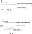
- Figs. 3 demonstrate examples of a circuitry that enables measuring the current (the "rotor” and the “stator” are interchangeable).
- Fig. 3A demonstrates the original hardware
- Fig. 3B demonstrates one possible option for hardware modification which enables measuring the capacitance change in time windows were the high driving signal does not exist.
- a driving pulse which is usually a periodically rectangular signal.
- the high voltage signal drives the operational amplifier to a saturation level and only afterwards the capacitance measurements will take place. Therefore only part of the capacitance change can be measured, this situation is demonstrated in Fig. 4A where 410, 410' and 410" represent blank time segments during which capacitance and particularly capacitance changes, cannot be measured.
- Fig. 4B demonstrates a solution that is not part of the present invention to cover the capacitance changes within a complete cycle.
- one driving pulse is omitted from time to time, thus enabling to measure the complete capacitance change curve cycle.
- 420 and 420" represent blank time segments during which the capacitance changes are not measured, while 420' represents a time segment where the pulse is omitted and the capacitance changes are measured. It is particularly convenient to omit a pulse during a period at which the scan accuracy is not critical, for instance during a vertical retrace time of a 2 x 1D of the scanning mirror, in projecting applications.
- Fig. 5 demonstrates the resulting voltage profile applied to the device.
- 510 is the base voltage that is applied to the device whereas 520 is the additional constant voltage applied to the device that is not part of the present invention for the capacitance changes measurements.
- the driving pulses (rectangle signals) 530 and 530" are examples of driving pulses that are responsible for the mirror movement, but as opposed to the similar profile presented mutatis mutandis in Fig. 2 , this time, there is no driving pulse 530' between pulses 530 and 530". Still, in order to achieve a better signal to noise ratio, it is possible to apply during the dilution period a high DC voltage (i.e.
- the dilution period being a period extending from the pulse that preceded the time at which the missing pulse should have been applied to the pulse that proceeds that time of the missing pulse). If the duration of the applied high DC voltage is essentially equal to one period, its effect would be negligible due to the energy conservation law. However, the current I in Eq. (5) will be much higher since it is proportional to the applied voltage, V.
- the data describing the capacitance changes may be applied for a variety of uses. For example, to determine if the mirror is actually rotating (this may be important for safety reasons, to avoid eye injuries when the laser beam is reflected from a non-moveable mirror), to measure the exact crossover time, i.e. the time when the mirror is parallel to the plane, etc. At that point, the capacitance is at its maximum value and apart from a small timing offset that could be compensated, the capacitance change at this point is equal to zero.
- the capacitance changes enable to determine the maximum deflection angle of the mirror. It is possible to measure it either according to the produced current (the higher dC v dt , the higher is the deflection) as exemplified in Fig. 6 or, according to the distance of the driving pulse and the crossover time.
- Fig. 7A is a side view of a typical in-plane mirror, where 710 is the holding frame that constitutes the base for the in-plane mirrors, 720 is an insulation layer, 730 is the rotor, 750 is the stator, and 740 is the overlapping area between the rotor (730) and the stator (750).
- a typical (but costly) solution is to add an optical detector to solve the ambiguity question.
- Another solution that could solve the ambiguity is to add a microphone as described in the Applicant's WO 2010/001388 .
- This embodiment which is not part of the present invention provides several symmetry breaking options that when applied to a MEMS device, they enable the determination of change in the direction movement of the mirror based on the capacitance change.
- the following examples provide non limiting forms of solving the 180° ambiguity.
- Fig. 7B illustrates breaking the inherent symmetry of the resonator mirror by adding a conductor plating.
- 760 is insulation plating whereas 770 is conductor plating placed on top of the insulation planting.
- Fig. 7C demonstrates breaking the inherent symmetry of the resonator mirror by reducing one side of the holding frame, 780 in this Fig. In both cases, using an additional capacitance sensing detector enables the detection of the mirror movement direction. It should be noted that instead of passive capacitance detection, it is possible to introduce active actuation voltage thereby ensuring that the mirror always starts at the correct direction.
- Figs. 8 provide simulated and practical results associated with some of the embodiments that are not part of the present invention that relate to the in-plane mirrors discussed above.
- Fig. 8A is a simulated detector signal (detector's current). In this simulation one can observe the complete capacitance change curve cycle where 810 and 820 are two reference points that are easily identifiable (further explanation on measuring the complete capacitance change curve cycle were provided hereinabove while discussing Fig. 4 ). The practical results are illustrated in Fig. 8B where the dilution method was applied in order to receive the full capacitance change curve.
- Blank time segments 830, 832, 834, 836 and 838 are associated with the voltage pulses where no measurements are made, and 810' and 820' are the points that correspond to the points of Fig. 8A , and were measured when a driving pulse was omitted.
- Fig. 8C presents the capacitance calculation of the new conductive layer of Fig. 7B using finite elements method (in pF).
- Fig. 9A demonstrates a schematic example of a staggered mirror device according to the present invention.
- the device comprises two types of "fingers", stator fingers (940) that are connected to MEMS handle (910), and rotor fingers (930) that are connected to the tilting mirror (950) and to ankle (920).
- Fig. 9B presents the same device in a side view for better demonstrating the fact that the "fingers" are staggered, i.e. are not at the same plane.
- Staggered mirrors are used for applications that require non-sinusoidal operation, such as vertical scan in projection systems, where a saw tooth movement is desirable.
- the driving voltage is usually continuous with the required characteristics that will cause the mirror to move according to a pre-defined path.
- a dynamic control is required to prevent the mirror from (slightly) rotating at its natural frequency.
- the driving voltage is typically continuous and cannot be replaced by a constant voltage as in the case of the in-plane mirror.
- the driving voltage is known and theoretically does not include "ripples" in the mirror resonance frequency, therefore, any "ripples" in the mirror resonance frequency may be attributed to capacitance change oscillations, i.e. the ripples in the capacitance measurements are created due to the high Q (low damping factor) of the mirror.
- a dynamic control is therefore needed to prevent the mirror from (slightly) rotating at its natural frequency.
- the applied voltage is continuous and cannot be replaced by a constant voltage as in the case of in-plane resonance mirror.
- the applied voltage is known and typically does not include “ripples” with the mirror resonance frequency. Therefore, any current "ripples" in the mirror resonance frequency is attributed to capacitance change oscillations, that is, to the mirror mechanical oscillations.
- Fig. 10 shows a typical case of staggered mirror having resonance "ripples" as measured by a circuitry similar to the one described in connection with Fig. 3B .
- the oscillations are clearly measured (1000 indicates the trace start) and it is possible to observe the oscillations decay in time due to mechanical losses.
- the oscillations are dynamically controlled (i.e. eradicated) by introducing a measurement metrics (such as p-p values or DFT value) and then eradicating the ripples by applying counter signals during the fly-back period.
- a measurement metrics such as p-p values or DFT value
- Other cancelling signals and/or minimizing algorithm such as early-late gate algorithm or any other control methods can be applied to achieve full eradication.
- Fig. 11 provides a flow chart that demonstrates one option for implementing the method proposed by the present invention.
- the current measurement provides the d CV dt , the measurement metrics are processed using a Discrete Fourier Transform (1110), and an early-late gate algorithm (1120) is used to identify the ripples.
- counter signals are applied to the driving circular (1130), preferably during the fly-back period to cancel the mirror ripples.
- a counter-acting signal is introduced. Two measurements are done. The first measurement is done with the current value of the counter-acting signal, while the second measurement is carried out with a slightly modified value. The metrics result of the first measurement is compared with the metrics result of the second measurement. If the second result shows a lower value (less ripples), the second counter-acting signal is considered to be better. The system will then adopt the second signal to be the reference signal and will continue the iterations while using the same trend for modification.
- the algorithm that is used to achieve the required results may be comprised of two or more modification dimensions such as amplitude and phase of the counter-acting signal.
Landscapes
- Physics & Mathematics (AREA)
- General Physics & Mathematics (AREA)
- Optics & Photonics (AREA)
- Micromachines (AREA)
- Mechanical Light Control Or Optical Switches (AREA)
Abstract
Description
- The present invention relates to optical systems for scanning or deflecting light beams, and in particularly to MEMS/MOEMS devices which comprise moving reflective elements, such as oscillating mirrors.
- Certain devices such as wafer defect scanners, laser printers, document scanners, projectors and the like make use of a narrow collimated laser beam that usually scan across a flat surface along a straight line path. A typical optical scanning system for this purpose employs a tilting flat mirror to deflect the beam. The tilting micro-mirror serves as a central element in many Micro Electro Mechanical Systems ("MEMS") devices and/or Micro Opto Electro Mechanical Systems ("MOEMS") devices. For the convenience of the reader, these devices (i.e. MEMS and/or MOEMS) will be referred to hereinafter throughout the specification and claims as "MEMS" devices. Many of these MEMS devices comprise two types of electro-statically mirrors:
- In-plane mirrors - this type of mirrors is usually driven at its resonance frequency, the stator and the rotor of these mirrors are at the same layer and the mirrors' driving pulse is usually of a rectangular type signal (these mirrors are also known as resonance mirrors).
- Staggered mirrors - this type of mirrors is typically comprised of two different layers, one that comprises the stator while the other comprises the rotor. In some cases, where the stator or the rotor is tilted permanently after manufacturing, only one layer may be used for the stator and the rotor. The staggered mirrors may operate at their resonance frequency or at lower frequencies down to and including DC (these mirrors are also known as linear mirrors).
- In most MEMS devices, data that relate to the mirror's position must be very accurate. Unfortunately, the knowledge of the actuation voltage timing is usually insufficient to enable determining the accurate position. Temperature changes, laser power change and other factors contribute to an overall unacceptable error in many cases, e.g. where a MEMS mirror is used for projecting applications that require accuracy of much less than a pixel. Video standards, especially high resolution use hundreds of bits per scan line, hence the significance in the accuracy of the mirror's position.
- There are several methods known in the art for monitoring the mirror's position, some of them rely on the electrostatic fingers to derive therefrom an indicator of the mirror position. Each position of the mirror is characterized by having different capacitance induced between the electrostatic fingers, thus, if the capacitance can be measured accurately, it may provide information regarding the mirror's position. The following attempts were made to harness the system capacitance for monitoring the mirror position:
-
US 2003174376 discloses a control system for controlling the position of the mirrors in a MEMS device. - This disclosure uses the absolute capacitance of the mirror to detect the position of the mirror. According to the solution described in this publication, the MEMS mirror device is mounted on a substrate that includes a micro mirror that is movable pivotally about an axis, a first conductive layer on the mirror, a second conductive layer on the substrate, where the first and second conductive layers form a capacitor for determining the position of the mirror. The control according to this disclosure is of the absolute phase by means of measuring the absolute phase of the mirror. Unfortunately measuring this parameter in order to overcome the problem at hand has been found quite unsatisfactory for a number of reasons among which is the parasitic capacitance involved.
-
US 2008180516 discloses a MEMS mirror device that includes a CMOS substrate, a pair of electrodes, and a reflecting mirror moveable over the substrate and the electrodes. The voltages applied to the electrodes create an electrostatic force causing the edge of the mirror to be attracted to the substrate. According to this publication the position of the mirror can be detected and controlled by sensing a change in capacitance between the mirror edges, by detecting the differential capacitance between the two antipodal electrodes. - The above methods measure the absolute capacitance but still fail to provide reliable and accurate information regarding to the mirror position because of parasitic capacitance that is inherent to the system. In addition due to the nature of the electric circle that drives the mirrors, none of the above methods can measure the capacitance throughout the whole scanning cycle.
- It is object of the present invention to provide a device and method for accurately monitoring the position of mirrors in a MEMS device.
- It is another object of the present invention to provide a device and method for measuring the changes in capacitance over time for a MEMS device.
- It is yet another object of the present invention to provide a device and method for measuring continuously the changes in capacitance in a MEMS device throughout the whole scanning cycle.
- It is still another object of the present invention to provide a method for monitoring the movement of at least one moveable mirror in a staggered configuration, based on identified plurality of ripples in the mirror resonance frequency.
- Other objects of the invention will become apparent as the description of the invention proceeds.
- According to the invention, a method for monitoring movement of at least one moveable mirror in a MEMS device and a MEMS device are provided, as defined in the appended claim.
- According to an embodiment of the present invention, monitoring is based upon capacitance changes in the MEMS device over time.
- In detail, the at least one moveable mirror is a staggered mirror, and the method comprises the steps of:
- a. measuring a current associated with the movement of the at least one moveable mirror;
- b. identifying a plurality of ripples associated with capacitance changes in the MEMS device over time, in the measured current; and
- c. monitoring the at least one moveable mirror movement based on the identified plurality of ripples.
- According to yet another embodiment of the present invention, the method further comprises the step of:
- d. establishing at least one counter signal (i.e. counter acting signal) required to offset at least one of the plurality of identified ripples to prevent unwanted oscillations in the movement of the at least one moveable mirror.
- The term "establishing at least one counter signal" as used herein should be understood to encompass also application of minimizing algorithms in order to establish the quantities of current/voltage required to offset (eradicate) the measured ripples.
- In accordance with another embodiment of the present invention, the method further comprises a step of determining the at least one mirror position based on the at least one mirror monitored movement.
- In accordance with another preferred embodiment, the method further comprises preventing the mirror from rotating at its natural frequency.
- According to another aspect of the present invention there is provided a MEMS device according to claim 5.
- In detail, the MEMS device comprises at least one moveable mirror and is adapted to monitor movement of the at least one moveable mirror based upon capacitance changes in the MEMS device over time, wherein the MEMS device further comprises:
- voltage supply means operative to provide driving voltage required for the movement of the at least one moveable mirror;
- current measuring means operative to measure current associated with a capacitance change involved with the movement of the at least one moveable mirror;
- a processor operative to monitor the movement of the at least one moveable mirror based on the current measurement; and
- wherein the MEMS device further comprises means to identify in the measured current a plurality of ripples associated with capacitance changes in the MEMS device over time, and the processor is adapted to monitor the movement of the at least one moveable mirror based on the plurality of identified ripples.
- In accordance with another preferred embodiment, a processor is further adapted to determine the at least one mirror position based upon the movement of the at least one mirror monitored.
- By yet another preferred embodiment, the processor is further operative to establish when the movement direction of the at least one mirror is changed based on the monitored movement of the at least one mirror.
- In accordance with yet another preferred embodiment, the processor is further adapted to prevent the mirror from rotating at its natural frequency (e.g. referred to hereinbefore as "ripples").
- Preferably, the processor is further adapted to establish at least one counter signal required to offset at least one of the plurality of identified ripples.
-
-
Fig. 1 displays a schematic example of MEMS mirrors apparatus; -
Fig. 2 presents a graph describing the voltage applied to in-plane mirrors dependence in time (that does not belong to the invention); -
Fig. 3 provides an example of a circuitry that enables measuring the current associated with the capacitance changes; -
Fig. 3A demonstrates prior art hardware; -
Fig. 3B demonstrates one possible option for hardware modification which enables the current measurement; -
Fig. 4 illustrates an embodiment that is not part of the present invention enabling capacitance measurements in a full cycle; -
Fig. 4A demonstrates measurements results when all actuation pulses exist. The repetitive high voltage pulses may blank relatively high percentage of the measurements; -
Fig. 4B demonstrates the measurement's results that is not part of the present invention when occasionally one actuation pulse is omitted to enable a clean full cycle of measurement; and -
Fig. 5 presents a graph describing the voltage applied to the in-plane mirrors illustrated inFig. 4B , which is not part of the invention; and -
Fig. 6 demonstrates a way to measure the maximum deflection angle of the mirror; and -
Fig. 7 illustrates an embodiment that is not part of the present invention for solving the "180° ambiguity" problem in in-plane mirrors; -
Fig 7A presents a side view of a typical prior-art in-plane mirror, that is not part of the present invention; -
Fig 7B demonstrates a solution for the "180° ambiguity" problem that is not part of the present invention; -
Fig 7C demonstrates another solution for the "180° ambiguity" problem that is not part of the present invention; -
Fig. 8 provides simulated and practical results which relate to in-plane mirrors that are not part of the invention; -
Fig. 8A presents a simulated detector signal that is not part of the invention; -
Fig. 8B illustrates practical results simulated inFig. 8A ; -
Fig. 8C displays the capacitance calculation of the new conductive layer as suggested inFig. 7B ; -
Figs. 9A and 9B demonstrate two views of a schematic example of a staggered mirror device according to the present invention; -
Fig. 10 presents a typical case of staggered mirror having resonance "ripples"; and -
Fig. 11 presents a flow chart demonstrating one option of implementing the method in the case of staggered mirrors. - A better understanding of the present invention may be obtained when the following non-limiting detailed examples are considered in conjunction with the accompanying drawings.
- In order to better understand the various aspects of the present invention, let us consider the following: Equation (1) is derived simply by using the basic definitions of the parameters used:

- I - is the current;
- Q - is the electric charge;
- C - is the capacitance; and
- V - is the voltage.
- In the classic case, the capacitance would remain constant over time, therefore the above equation may be reduced to the following:

- However, according to a preferred embodiment of the present invention, we are interested in the capacitance change when fixed in time voltage is applied to the system. In this case, equation (1) may be reduced to the following:

- In this case the current will indicate the change in the capacitance with time. Now, let us assume that the capacitance is composed of fixed and variable components:

- The parasitic capacitance associated with the fixed capacitance will not be detected when we measure only the change in capacitance, hence:

- As aforesaid, many MEMS devices comprise in-plane mirrors and/or staggered mirrors. The following description relates to these two types of mirrors outlining the difference in implementing the method of the in-plane mirrors case, which is not part of the invention, with respect to the staggered mirror one.
-
Fig. 1 illustrates a schematic example of an in-plane mirror that it is not part of the invention.Device 100 comprises two types of "fingers", the rotor fingers (110) that are connected to the tilting mirror and the stator fingers (120) that are connected to MEMS structure (where both types of fingers reside at the same plane), and a torsional spring (130) that enables the movable MEMS part to move. - A fixed voltage is applied to the device.
Fig. 2 illustrates the voltage profile over time that is applied to the in-plane mirrors. 210 shows the base level of constant voltage applied to a typical prior art device, whereas 220, 220' and 220" are the rectangular signals that form the driving pulse. A relatively small fixedDC voltage 230 is further applied to the device, in order to enable measuring capacitance changes. The small fixed DC voltage may be either positive or negative, and is selected such that it will preferably have a negligible effect on the mirror operation. Still, it will be such that will enable the measurement of the current evolving due to the change in the capacitance. -
Figs. 3 demonstrate examples of a circuitry that enables measuring the current (the "rotor" and the "stator" are interchangeable).Fig. 3A demonstrates the original hardware, andFig. 3B demonstrates one possible option for hardware modification which enables measuring the capacitance change in time windows were the high driving signal does not exist. - The movement of the in-plane mirror is driven by a driving pulse which is usually a periodically rectangular signal. The high voltage signal drives the operational amplifier to a saturation level and only afterwards the capacitance measurements will take place. Therefore only part of the capacitance change can be measured, this situation is demonstrated in
Fig. 4A where 410, 410' and 410" represent blank time segments during which capacitance and particularly capacitance changes, cannot be measured.Fig. 4B demonstrates a solution that is not part of the present invention to cover the capacitance changes within a complete cycle. According to one embodiment that is not part of the present invention, one driving pulse is omitted from time to time, thus enabling to measure the complete capacitance change curve cycle. 420 and 420" represent blank time segments during which the capacitance changes are not measured, while 420' represents a time segment where the pulse is omitted and the capacitance changes are measured. It is particularly convenient to omit a pulse during a period at which the scan accuracy is not critical, for instance during a vertical retrace time of a 2 x 1D of the scanning mirror, in projecting applications. -
Fig. 5 demonstrates the resulting voltage profile applied to the device. Here again, 510 is the base voltage that is applied to the device whereas 520 is the additional constant voltage applied to the device that is not part of the present invention for the capacitance changes measurements. The driving pulses (rectangle signals) 530 and 530" are examples of driving pulses that are responsible for the mirror movement, but as opposed to the similar profile presented mutatis mutandis inFig. 2 , this time, there is no driving pulse 530' betweenpulses - The data describing the capacitance changes may be applied for a variety of uses. For example, to determine if the mirror is actually rotating (this may be important for safety reasons, to avoid eye injuries when the laser beam is reflected from a non-moveable mirror), to measure the exact crossover time, i.e. the time when the mirror is parallel to the plane, etc. At that point, the capacitance is at its maximum value and apart from a small timing offset that could be compensated, the capacitance change at this point is equal to zero. The capacitance changes enable to determine the maximum deflection angle of the mirror. It is possible to measure it either according to the produced current (the higher

Fig. 6 or, according to the distance of the driving pulse and the crossover time. - Due to the full symmetry existing typically in in-plane mirrors, it is usually impossible to determine whether the mirror moves upward or downward. This problem is usually referred to as the "180° ambiguity". At a certain occasion, the mirror may start moving in one direction, while, at another occasion it may start moving in the opposite direction.
Fig. 7A is a side view of a typical in-plane mirror, where 710 is the holding frame that constitutes the base for the in-plane mirrors, 720 is an insulation layer, 730 is the rotor, 750 is the stator, and 740 is the overlapping area between the rotor (730) and the stator (750). Several solutions to this "180° ambiguity" problem are known in the art. A typical (but costly) solution is to add an optical detector to solve the ambiguity question. Another solution that could solve the ambiguity is to add a microphone as described in the Applicant'sWO 2010/001388 . This embodiment, which is not part of the present invention provides several symmetry breaking options that when applied to a MEMS device, they enable the determination of change in the direction movement of the mirror based on the capacitance change. The following examples provide non limiting forms of solving the 180° ambiguity. -
Fig. 7B illustrates breaking the inherent symmetry of the resonator mirror by adding a conductor plating. In this Figure, 760 is insulation plating whereas 770 is conductor plating placed on top of the insulation planting.Fig. 7C demonstrates breaking the inherent symmetry of the resonator mirror by reducing one side of the holding frame, 780 in this Fig. In both cases, using an additional capacitance sensing detector enables the detection of the mirror movement direction. It should be noted that instead of passive capacitance detection, it is possible to introduce active actuation voltage thereby ensuring that the mirror always starts at the correct direction. -
Figs. 8 provide simulated and practical results associated with some of the embodiments that are not part of the present invention that relate to the in-plane mirrors discussed above.Fig. 8A is a simulated detector signal (detector's current). In this simulation one can observe the complete capacitance change curve cycle where 810 and 820 are two reference points that are easily identifiable (further explanation on measuring the complete capacitance change curve cycle were provided hereinabove while discussingFig. 4 ). The practical results are illustrated inFig. 8B where the dilution method was applied in order to receive the full capacitance change curve.Blank time segments Fig. 8A , and were measured when a driving pulse was omitted.Fig. 8C presents the capacitance calculation of the new conductive layer ofFig. 7B using finite elements method (in pF). -
Fig. 9A demonstrates a schematic example of a staggered mirror device according to the present invention. The device comprises two types of "fingers", stator fingers (940) that are connected to MEMS handle (910), and rotor fingers (930) that are connected to the tilting mirror (950) and to ankle (920).Fig. 9B presents the same device in a side view for better demonstrating the fact that the "fingers" are staggered, i.e. are not at the same plane. - Staggered mirrors are used for applications that require non-sinusoidal operation, such as vertical scan in projection systems, where a saw tooth movement is desirable. For this purpose, the driving voltage is usually continuous with the required characteristics that will cause the mirror to move according to a pre-defined path. However a dynamic control is required to prevent the mirror from (slightly) rotating at its natural frequency. As may be recalled from Equation (1), the measured current depends on the voltage change in time and the capacitance change in time:

- But in the staggered mirror case, the driving voltage is typically continuous and cannot be replaced by a constant voltage as in the case of the in-plane mirror. However, the driving voltage is known and theoretically does not include "ripples" in the mirror resonance frequency, therefore, any "ripples" in the mirror resonance frequency may be attributed to capacitance change oscillations, i.e. the ripples in the capacitance measurements are created due to the high Q (low damping factor) of the mirror.
- A dynamic control is therefore needed to prevent the mirror from (slightly) rotating at its natural frequency.
- As demonstrated hereinbefore, the current that can be measured will be:

- But in this case, the applied voltage is continuous and cannot be replaced by a constant voltage as in the case of in-plane resonance mirror. However, the applied voltage is known and typically does not include "ripples" with the mirror resonance frequency. Therefore, any current "ripples" in the mirror resonance frequency is attributed to capacitance change oscillations, that is, to the mirror mechanical oscillations.
-
Fig. 10 shows a typical case of staggered mirror having resonance "ripples" as measured by a circuitry similar to the one described in connection withFig. 3B . The oscillations are clearly measured (1000 indicates the trace start) and it is possible to observe the oscillations decay in time due to mechanical losses. According to a preferred embodiment of the present invention, the oscillations are dynamically controlled (i.e. eradicated) by introducing a measurement metrics (such as p-p values or DFT value) and then eradicating the ripples by applying counter signals during the fly-back period. Other cancelling signals and/or minimizing algorithm such as early-late gate algorithm or any other control methods can be applied to achieve full eradication. -
Fig. 11 provides a flow chart that demonstrates one option for implementing the method proposed by the present invention. The current measurement provides the
- In order to minimize the ripples, a counter-acting signal is introduced. Two measurements are done. The first measurement is done with the current value of the counter-acting signal, while the second measurement is carried out with a slightly modified value. The metrics result of the first measurement is compared with the metrics result of the second measurement. If the second result shows a lower value (less ripples), the second counter-acting signal is considered to be better. The system will then adopt the second signal to be the reference signal and will continue the iterations while using the same trend for modification.
- However in case the second measurement yields a higher value result (i.e. more ripples), the selected modification would be considered to worsen the situation, so that the system would stay in this case with the same original state and will apply a reverse modification trend.
- It should be mentioned that the algorithm that is used to achieve the required results may be comprised of two or more modification dimensions such as amplitude and phase of the counter-acting signal.
Claims (6)
- A method for monitoring movement of at least one moveable mirror in a MEMS device which comprises one or more moveable mirrors, wherein said at least one moveable mirror is a staggered mirror, said monitoring is based upon capacitance changes in said MEMS device over time,
said method comprising the steps of:a. measuring a current associated with the movement of said at least one moveable mirror;b. identifying a plurality of ripples associated with capacitance changes in said MEMS device over time, in said measured current; andc. monitoring said at least one moveable mirror movement based on the identified plurality of ripples. - A method according to claim 1, further comprising:d. establishing at least one counter signal required to offset at least one of said plurality of identified ripples to prevent unwanted oscillations in the movement of said at least one moveable mirror.
- A method according to claim 1, further comprising determining said at least one mirror position based upon said at least one mirror monitored movement.
- A method according to claim 1, further comprising preventing said mirror from rotating at its natural frequency.
- A MEMS device comprising at least one moveable mirror and adapted to monitor movement of said at least one moveable mirror based upon capacitance changes in said MEMS device over time, said at least one moveable mirror being a staggered mirror further comprising:voltage supply means operative to provide driving voltage required for the movement of said at least one moveable mirror;current measuring means operative to measure current associated with a capacitance change involved with the movement of said at least one moveable mirror;a processor operative to monitor the movement of said at least one moveable mirror based on said current measurement; andmeans to identify in the measured current a plurality of ripples associated with capacitance changes in said MEMS device over time;wherein said processor is adapted to monitor the movement of said at least one moveable mirror based on said plurality of identified ripples.
- A MEMS device according to claim 5, wherein said processor is further adapted to determine said at least one mirror position based upon the movement of said at least one mirror monitored.
Applications Claiming Priority (2)
| Application Number | Priority Date | Filing Date | Title |
|---|---|---|---|
| IL201811A IL201811A0 (en) | 2009-10-29 | 2009-10-29 | Method and device for monitoring movement of mirrors in a mems device |
| EP10189155.4A EP2339390B1 (en) | 2009-10-29 | 2010-10-28 | Method and device for monitoring movement of mirrors in a MEMS device |
Related Parent Applications (2)
| Application Number | Title | Priority Date | Filing Date |
|---|---|---|---|
| EP10189155.4A Division EP2339390B1 (en) | 2009-10-29 | 2010-10-28 | Method and device for monitoring movement of mirrors in a MEMS device |
| EP10189155.4A Division-Into EP2339390B1 (en) | 2009-10-29 | 2010-10-28 | Method and device for monitoring movement of mirrors in a MEMS device |
Publications (2)
| Publication Number | Publication Date |
|---|---|
| EP3232246A1 true EP3232246A1 (en) | 2017-10-18 |
| EP3232246B1 EP3232246B1 (en) | 2023-05-10 |
Family
ID=42263458
Family Applications (2)
| Application Number | Title | Priority Date | Filing Date |
|---|---|---|---|
| EP17171014.8A Active EP3232246B1 (en) | 2009-10-29 | 2010-10-28 | Method and device for monitoring movement of mirrors in a mems device |
| EP10189155.4A Active EP2339390B1 (en) | 2009-10-29 | 2010-10-28 | Method and device for monitoring movement of mirrors in a MEMS device |
Family Applications After (1)
| Application Number | Title | Priority Date | Filing Date |
|---|---|---|---|
| EP10189155.4A Active EP2339390B1 (en) | 2009-10-29 | 2010-10-28 | Method and device for monitoring movement of mirrors in a MEMS device |
Country Status (4)
| Country | Link |
|---|---|
| US (1) | US8553308B2 (en) |
| EP (2) | EP3232246B1 (en) |
| JP (1) | JP5847391B2 (en) |
| IL (1) | IL201811A0 (en) |
Families Citing this family (22)
| Publication number | Priority date | Publication date | Assignee | Title |
|---|---|---|---|---|
| WO2013030842A1 (en) | 2011-09-04 | 2013-03-07 | Maradin Technologies Ltd. | Apparatus and methods for locking resonating frequency of a miniature system |
| JP5988592B2 (en) * | 2012-01-19 | 2016-09-07 | キヤノン株式会社 | Movable mirror, wavefront correction device and fundus examination apparatus |
| ITTO20120758A1 (en) | 2012-08-31 | 2014-03-01 | St Microelectronics Srl | MEMS DEVICE INCLUDING A MOBILE ELEMENT AND A RESISTIVE SENSOR, AND GENERATION METHOD OF AN INDICATIVE SIGNAL OF THE POSITION OF THE MOBILE ELEMENT |
| DE102012218219A1 (en) * | 2012-10-05 | 2014-04-10 | Carl Zeiss Smt Gmbh | Method for controlling the tilting of a mirror element |
| ITTO20131014A1 (en) * | 2013-12-12 | 2015-06-13 | St Microelectronics Int Nv | ELECTROSTATICALLY ACTIVATED OSCILLATING STRUCTURE WITH CONTROL OF THE START OSCILLATION PHASE, AND RELATED METHOD OF MANUFACTURE AND PILOT METHOD |
| US9784558B2 (en) * | 2014-01-20 | 2017-10-10 | Apple Inc. | Sensing of mirror position using fringing fields |
| US9740002B2 (en) | 2015-11-10 | 2017-08-22 | Stmicroelectronics Ltd | Controlling opening angle of a resonating mirror |
| US9810902B1 (en) | 2016-06-24 | 2017-11-07 | Stmicroelectronics Ltd | Opening angle measurement of an oscillating MEMS mirror |
| IT201600079604A1 (en) | 2016-07-28 | 2018-01-28 | St Microelectronics Srl | OSCILLATING STRUCTURE WITH PIEZOELECTRIC IMPLEMENTATION, SYSTEM AND MANUFACTURING METHOD |
| US10473920B2 (en) | 2016-08-24 | 2019-11-12 | Stmicroelectronics S.R.L. | Hermetically sealed MEMS mirror and method of manufacture |
| US10228555B2 (en) | 2016-09-06 | 2019-03-12 | Stmicroelectronics Ltd | Resonance MEMS mirror control system |
| US10365474B2 (en) | 2017-06-05 | 2019-07-30 | Stmicroelectronics Ltd | Phase error measurement for oscillating mirrors |
| US10908361B2 (en) | 2018-06-06 | 2021-02-02 | Apple Inc. | Capacitive position sensing for capacitive drive MEMS devices |
| DE102018114388A1 (en) | 2018-06-15 | 2019-12-19 | Valeo Schalter Und Sensoren Gmbh | Method for controlling a drive device of a micro-oscillating mirror, control device and deflecting mirror device |
| DE102018124964A1 (en) * | 2018-10-10 | 2020-04-16 | Valeo Schalter Und Sensoren Gmbh | Method for controlling a drive device of a micro oscillating mirror, control device and deflecting mirror device |
| DE102018124960A1 (en) * | 2018-10-10 | 2020-04-16 | Valeo Schalter Und Sensoren Gmbh | Method for controlling a drive device of a micro oscillating mirror, control device and deflecting mirror device |
| CN110333598B (en) * | 2019-04-29 | 2021-04-23 | 西安知微传感技术有限公司 | Method and circuit for acquiring capacitance feedback signal of capacitance feedback type micro torsion mirror |
| IT202000001411A1 (en) | 2020-01-24 | 2021-07-24 | St Microelectronics Srl | PROCESSING METHOD OF A SLICE FOR THE MANUFACTURE OF AN OSCILLATING STRUCTURE SUCH AS A MICRO-MIRROR |
| US11467394B2 (en) | 2020-02-28 | 2022-10-11 | Infineon Technologies Ag | Capacitive charge based self-sensing and position observer for electrostatic MEMS mirrors |
| US20220269069A1 (en) * | 2020-04-03 | 2022-08-25 | Google Llc | Technique to detect the rotational direction of resonant mems mirrors driven by parametric excitation |
| US11835710B2 (en) * | 2020-12-15 | 2023-12-05 | Infineon Technologies Ag | Method of mode coupling detection and damping and usage for electrostatic MEMS mirrors |
| KR20250108467A (en) | 2024-01-08 | 2025-07-15 | 주식회사 위멤스 | MEMS Scanner Package Including MEMS Scanner Mirror Rotation Angle Sensing Device |
Citations (5)
| Publication number | Priority date | Publication date | Assignee | Title |
|---|---|---|---|---|
| US20030174376A1 (en) | 2002-03-12 | 2003-09-18 | Corning Incorporated | Pointing angle control of electrostatic micro mirrors with modified sliding mode control algorithm for precision control |
| US20040233507A1 (en) * | 2003-05-20 | 2004-11-25 | Henry Chu | Damped control of a micromechanical device |
| US20080180516A1 (en) | 2007-01-26 | 2008-07-31 | Miradia Inc. | Mems mirror system for laser printing applications |
| US20090244668A1 (en) * | 2008-04-01 | 2009-10-01 | Kabushiki Kaisha Topcon | Method of driving mems mirror scanner, method of driving mems actuator scanner and method of controlling rotation angle of mems actuator |
| WO2010001388A1 (en) | 2008-07-02 | 2010-01-07 | Btendo Ltd. | A mems device comprising oscillations' measurements means |
Family Cites Families (10)
| Publication number | Priority date | Publication date | Assignee | Title |
|---|---|---|---|---|
| US5061049A (en) * | 1984-08-31 | 1991-10-29 | Texas Instruments Incorporated | Spatial light modulator and method |
| US5096279A (en) * | 1984-08-31 | 1992-03-17 | Texas Instruments Incorporated | Spatial light modulator and method |
| US5172262A (en) * | 1985-10-30 | 1992-12-15 | Texas Instruments Incorporated | Spatial light modulator and method |
| US6201629B1 (en) * | 1997-08-27 | 2001-03-13 | Microoptical Corporation | Torsional micro-mechanical mirror system |
| US6694072B1 (en) * | 1999-07-21 | 2004-02-17 | Armand P. Neukermans | Flexible, modular, compact fiber switch improvements |
| AU2003282286A1 (en) * | 2002-12-10 | 2004-06-30 | Koninklijke Philips Electronics N.V. | Transducer and electronic device |
| JP4357317B2 (en) * | 2003-05-13 | 2009-11-04 | 富士通株式会社 | Tilt mirror control device and control method |
| JP2007256557A (en) * | 2006-03-23 | 2007-10-04 | Sumitomo Precision Prod Co Ltd | MEMS actuator and scanning device |
| US20080001850A1 (en) * | 2006-06-06 | 2008-01-03 | Mark Champion | Beam scanner with reduced phase error |
| US7999244B2 (en) * | 2007-12-18 | 2011-08-16 | Microvision, Inc. | MEMS devices and related scanned beam devices |
-
2009
- 2009-10-29 IL IL201811A patent/IL201811A0/en unknown
-
2010
- 2010-10-28 EP EP17171014.8A patent/EP3232246B1/en active Active
- 2010-10-28 EP EP10189155.4A patent/EP2339390B1/en active Active
- 2010-10-29 JP JP2010243325A patent/JP5847391B2/en active Active
- 2010-10-29 US US12/915,295 patent/US8553308B2/en active Active
Patent Citations (5)
| Publication number | Priority date | Publication date | Assignee | Title |
|---|---|---|---|---|
| US20030174376A1 (en) | 2002-03-12 | 2003-09-18 | Corning Incorporated | Pointing angle control of electrostatic micro mirrors with modified sliding mode control algorithm for precision control |
| US20040233507A1 (en) * | 2003-05-20 | 2004-11-25 | Henry Chu | Damped control of a micromechanical device |
| US20080180516A1 (en) | 2007-01-26 | 2008-07-31 | Miradia Inc. | Mems mirror system for laser printing applications |
| US20090244668A1 (en) * | 2008-04-01 | 2009-10-01 | Kabushiki Kaisha Topcon | Method of driving mems mirror scanner, method of driving mems actuator scanner and method of controlling rotation angle of mems actuator |
| WO2010001388A1 (en) | 2008-07-02 | 2010-01-07 | Btendo Ltd. | A mems device comprising oscillations' measurements means |
Also Published As
| Publication number | Publication date |
|---|---|
| JP2011123481A (en) | 2011-06-23 |
| IL201811A0 (en) | 2010-06-16 |
| EP3232246B1 (en) | 2023-05-10 |
| US20110109951A1 (en) | 2011-05-12 |
| JP5847391B2 (en) | 2016-01-20 |
| US8553308B2 (en) | 2013-10-08 |
| EP2339390A1 (en) | 2011-06-29 |
| EP2339390B1 (en) | 2018-12-05 |
Similar Documents
| Publication | Publication Date | Title |
|---|---|---|
| EP3232246B1 (en) | Method and device for monitoring movement of mirrors in a mems device | |
| US10768410B2 (en) | Detection of amplitude, regulation of amplitude and detection of direction of an oscillation of an oscillatory body | |
| EP2940509B1 (en) | Apparatus and method for driving and measuring a MEMS mirror system | |
| US7095494B2 (en) | Method and apparatus for measuring temporal response characteristics of digital mirror devices | |
| US20150204650A1 (en) | Sensing of mirror position using fringing fields | |
| EP3290985B1 (en) | Resonance mems mirror control system | |
| US20070159189A1 (en) | Apparatus and method for evaluating driving characteristics of scanner | |
| US8068230B2 (en) | Real-time measurement of ultrashort laser pulses | |
| JP2009265608A (en) | Method of driving mems mirror scanner, method of driving mems actuator scanner and method of controlling rotation angle of mems actuator | |
| US10345577B2 (en) | Controlling opening angle of a resonating mirror | |
| US8848196B2 (en) | Spectrophotometer having prompt spectrophotometric measurement | |
| US20110320046A1 (en) | Drive method for starting and operating a resonant scanning MEMS device at its resonant frequency | |
| Zhang et al. | An integrated capacitive sensing method for electrostatic comb-drive micromirrors | |
| US20150185468A1 (en) | Driving calibration apparatus of electrostatic mems scanning mirror and driving calibration method therefof | |
| KR102207614B1 (en) | Driving Method for MEMS Mirror Scanner and Driving Device for MEMS Mirror Scanner using the method thereof | |
| EP2555037A1 (en) | Variable spectral element | |
| US7365613B2 (en) | Method of determining resonant frequency | |
| CN104950142B (en) | Method for measuring vibration characteristics of cantilever and device for measuring vibration characteristics of cantilever | |
| EP2735870A1 (en) | Modulator monitoring during measuring electromobility | |
| KR101160804B1 (en) | Method for detecting of optical surface profilometer | |
| Strozewski et al. | Characterization of a micromechanical spatial light modulator | |
| Portelli et al. | Resonant micro-mirror electrical characterisation towards tunable digital drive circuit design | |
| Schuster et al. | Investigations on an Integrated Optical Position Detection of Micromachined Scanning Mirrors | |
| JPH08219706A (en) | Distance measuring method and device |
Legal Events
| Date | Code | Title | Description |
|---|---|---|---|
| PUAI | Public reference made under article 153(3) epc to a published international application that has entered the european phase |
Free format text: ORIGINAL CODE: 0009012 |
|
| STAA | Information on the status of an ep patent application or granted ep patent |
Free format text: STATUS: THE APPLICATION HAS BEEN PUBLISHED |
|
| AC | Divisional application: reference to earlier application |
Ref document number: 2339390 Country of ref document: EP Kind code of ref document: P |
|
| AK | Designated contracting states |
Kind code of ref document: A1 Designated state(s): AL AT BE BG CH CY CZ DE DK EE ES FI FR GB GR HR HU IE IS IT LI LT LU LV MC MK MT NL NO PL PT RO RS SE SI SK SM TR |
|
| STAA | Information on the status of an ep patent application or granted ep patent |
Free format text: STATUS: REQUEST FOR EXAMINATION WAS MADE |
|
| 17P | Request for examination filed |
Effective date: 20180416 |
|
| RBV | Designated contracting states (corrected) |
Designated state(s): AL AT BE BG CH CY CZ DE DK EE ES FI FR GB GR HR HU IE IS IT LI LT LU LV MC MK MT NL NO PL PT RO RS SE SI SK SM TR |
|
| STAA | Information on the status of an ep patent application or granted ep patent |
Free format text: STATUS: EXAMINATION IS IN PROGRESS |
|
| 17Q | First examination report despatched |
Effective date: 20201009 |
|
| GRAP | Despatch of communication of intention to grant a patent |
Free format text: ORIGINAL CODE: EPIDOSNIGR1 |
|
| STAA | Information on the status of an ep patent application or granted ep patent |
Free format text: STATUS: GRANT OF PATENT IS INTENDED |
|
| INTG | Intention to grant announced |
Effective date: 20220802 |
|
| GRAJ | Information related to disapproval of communication of intention to grant by the applicant or resumption of examination proceedings by the epo deleted |
Free format text: ORIGINAL CODE: EPIDOSDIGR1 |
|
| STAA | Information on the status of an ep patent application or granted ep patent |
Free format text: STATUS: EXAMINATION IS IN PROGRESS |
|
| INTC | Intention to grant announced (deleted) | ||
| GRAP | Despatch of communication of intention to grant a patent |
Free format text: ORIGINAL CODE: EPIDOSNIGR1 |
|
| STAA | Information on the status of an ep patent application or granted ep patent |
Free format text: STATUS: GRANT OF PATENT IS INTENDED |
|
| INTG | Intention to grant announced |
Effective date: 20221128 |
|
| GRAS | Grant fee paid |
Free format text: ORIGINAL CODE: EPIDOSNIGR3 |
|
| GRAA | (expected) grant |
Free format text: ORIGINAL CODE: 0009210 |
|
| STAA | Information on the status of an ep patent application or granted ep patent |
Free format text: STATUS: THE PATENT HAS BEEN GRANTED |
|
| RAP3 | Party data changed (applicant data changed or rights of an application transferred) |
Owner name: STMICROELECTRONICS INTERNATIONAL N.V. |
|
| AC | Divisional application: reference to earlier application |
Ref document number: 2339390 Country of ref document: EP Kind code of ref document: P |
|
| AK | Designated contracting states |
Kind code of ref document: B1 Designated state(s): AL AT BE BG CH CY CZ DE DK EE ES FI FR GB GR HR HU IE IS IT LI LT LU LV MC MK MT NL NO PL PT RO RS SE SI SK SM TR |
|
| REG | Reference to a national code |
Ref country code: GB Ref legal event code: FG4D |
|
| REG | Reference to a national code |
Ref country code: AT Ref legal event code: REF Ref document number: 1567247 Country of ref document: AT Kind code of ref document: T Effective date: 20230515 Ref country code: CH Ref legal event code: EP |
|
| REG | Reference to a national code |
Ref country code: DE Ref legal event code: R096 Ref document number: 602010068796 Country of ref document: DE |
|
| REG | Reference to a national code |
Ref country code: IE Ref legal event code: FG4D |
|
| REG | Reference to a national code |
Ref country code: LT Ref legal event code: MG9D |
|
| REG | Reference to a national code |
Ref country code: NL Ref legal event code: MP Effective date: 20230510 |
|
| REG | Reference to a national code |
Ref country code: AT Ref legal event code: MK05 Ref document number: 1567247 Country of ref document: AT Kind code of ref document: T Effective date: 20230510 |
|
| PG25 | Lapsed in a contracting state [announced via postgrant information from national office to epo] |
Ref country code: SE Free format text: LAPSE BECAUSE OF FAILURE TO SUBMIT A TRANSLATION OF THE DESCRIPTION OR TO PAY THE FEE WITHIN THE PRESCRIBED TIME-LIMIT Effective date: 20230510 Ref country code: PT Free format text: LAPSE BECAUSE OF FAILURE TO SUBMIT A TRANSLATION OF THE DESCRIPTION OR TO PAY THE FEE WITHIN THE PRESCRIBED TIME-LIMIT Effective date: 20230911 Ref country code: NO Free format text: LAPSE BECAUSE OF FAILURE TO SUBMIT A TRANSLATION OF THE DESCRIPTION OR TO PAY THE FEE WITHIN THE PRESCRIBED TIME-LIMIT Effective date: 20230810 Ref country code: NL Free format text: LAPSE BECAUSE OF FAILURE TO SUBMIT A TRANSLATION OF THE DESCRIPTION OR TO PAY THE FEE WITHIN THE PRESCRIBED TIME-LIMIT Effective date: 20230510 Ref country code: ES Free format text: LAPSE BECAUSE OF FAILURE TO SUBMIT A TRANSLATION OF THE DESCRIPTION OR TO PAY THE FEE WITHIN THE PRESCRIBED TIME-LIMIT Effective date: 20230510 Ref country code: AT Free format text: LAPSE BECAUSE OF FAILURE TO SUBMIT A TRANSLATION OF THE DESCRIPTION OR TO PAY THE FEE WITHIN THE PRESCRIBED TIME-LIMIT Effective date: 20230510 |
|
| PG25 | Lapsed in a contracting state [announced via postgrant information from national office to epo] |
Ref country code: RS Free format text: LAPSE BECAUSE OF FAILURE TO SUBMIT A TRANSLATION OF THE DESCRIPTION OR TO PAY THE FEE WITHIN THE PRESCRIBED TIME-LIMIT Effective date: 20230510 Ref country code: PL Free format text: LAPSE BECAUSE OF FAILURE TO SUBMIT A TRANSLATION OF THE DESCRIPTION OR TO PAY THE FEE WITHIN THE PRESCRIBED TIME-LIMIT Effective date: 20230510 Ref country code: LV Free format text: LAPSE BECAUSE OF FAILURE TO SUBMIT A TRANSLATION OF THE DESCRIPTION OR TO PAY THE FEE WITHIN THE PRESCRIBED TIME-LIMIT Effective date: 20230510 Ref country code: LT Free format text: LAPSE BECAUSE OF FAILURE TO SUBMIT A TRANSLATION OF THE DESCRIPTION OR TO PAY THE FEE WITHIN THE PRESCRIBED TIME-LIMIT Effective date: 20230510 Ref country code: IS Free format text: LAPSE BECAUSE OF FAILURE TO SUBMIT A TRANSLATION OF THE DESCRIPTION OR TO PAY THE FEE WITHIN THE PRESCRIBED TIME-LIMIT Effective date: 20230910 Ref country code: HR Free format text: LAPSE BECAUSE OF FAILURE TO SUBMIT A TRANSLATION OF THE DESCRIPTION OR TO PAY THE FEE WITHIN THE PRESCRIBED TIME-LIMIT Effective date: 20230510 Ref country code: GR Free format text: LAPSE BECAUSE OF FAILURE TO SUBMIT A TRANSLATION OF THE DESCRIPTION OR TO PAY THE FEE WITHIN THE PRESCRIBED TIME-LIMIT Effective date: 20230811 |
|
| PG25 | Lapsed in a contracting state [announced via postgrant information from national office to epo] |
Ref country code: FI Free format text: LAPSE BECAUSE OF FAILURE TO SUBMIT A TRANSLATION OF THE DESCRIPTION OR TO PAY THE FEE WITHIN THE PRESCRIBED TIME-LIMIT Effective date: 20230510 |
|
| PG25 | Lapsed in a contracting state [announced via postgrant information from national office to epo] |
Ref country code: SK Free format text: LAPSE BECAUSE OF FAILURE TO SUBMIT A TRANSLATION OF THE DESCRIPTION OR TO PAY THE FEE WITHIN THE PRESCRIBED TIME-LIMIT Effective date: 20230510 |
|
| PG25 | Lapsed in a contracting state [announced via postgrant information from national office to epo] |
Ref country code: SM Free format text: LAPSE BECAUSE OF FAILURE TO SUBMIT A TRANSLATION OF THE DESCRIPTION OR TO PAY THE FEE WITHIN THE PRESCRIBED TIME-LIMIT Effective date: 20230510 Ref country code: SK Free format text: LAPSE BECAUSE OF FAILURE TO SUBMIT A TRANSLATION OF THE DESCRIPTION OR TO PAY THE FEE WITHIN THE PRESCRIBED TIME-LIMIT Effective date: 20230510 Ref country code: RO Free format text: LAPSE BECAUSE OF FAILURE TO SUBMIT A TRANSLATION OF THE DESCRIPTION OR TO PAY THE FEE WITHIN THE PRESCRIBED TIME-LIMIT Effective date: 20230510 Ref country code: EE Free format text: LAPSE BECAUSE OF FAILURE TO SUBMIT A TRANSLATION OF THE DESCRIPTION OR TO PAY THE FEE WITHIN THE PRESCRIBED TIME-LIMIT Effective date: 20230510 Ref country code: DK Free format text: LAPSE BECAUSE OF FAILURE TO SUBMIT A TRANSLATION OF THE DESCRIPTION OR TO PAY THE FEE WITHIN THE PRESCRIBED TIME-LIMIT Effective date: 20230510 Ref country code: CZ Free format text: LAPSE BECAUSE OF FAILURE TO SUBMIT A TRANSLATION OF THE DESCRIPTION OR TO PAY THE FEE WITHIN THE PRESCRIBED TIME-LIMIT Effective date: 20230510 |
|
| REG | Reference to a national code |
Ref country code: DE Ref legal event code: R097 Ref document number: 602010068796 Country of ref document: DE |
|
| PLBE | No opposition filed within time limit |
Free format text: ORIGINAL CODE: 0009261 |
|
| STAA | Information on the status of an ep patent application or granted ep patent |
Free format text: STATUS: NO OPPOSITION FILED WITHIN TIME LIMIT |
|
| 26N | No opposition filed |
Effective date: 20240213 |
|
| PG25 | Lapsed in a contracting state [announced via postgrant information from national office to epo] |
Ref country code: SI Free format text: LAPSE BECAUSE OF FAILURE TO SUBMIT A TRANSLATION OF THE DESCRIPTION OR TO PAY THE FEE WITHIN THE PRESCRIBED TIME-LIMIT Effective date: 20230510 |
|
| PG25 | Lapsed in a contracting state [announced via postgrant information from national office to epo] |
Ref country code: SI Free format text: LAPSE BECAUSE OF FAILURE TO SUBMIT A TRANSLATION OF THE DESCRIPTION OR TO PAY THE FEE WITHIN THE PRESCRIBED TIME-LIMIT Effective date: 20230510 Ref country code: IT Free format text: LAPSE BECAUSE OF FAILURE TO SUBMIT A TRANSLATION OF THE DESCRIPTION OR TO PAY THE FEE WITHIN THE PRESCRIBED TIME-LIMIT Effective date: 20230510 Ref country code: MC Free format text: LAPSE BECAUSE OF FAILURE TO SUBMIT A TRANSLATION OF THE DESCRIPTION OR TO PAY THE FEE WITHIN THE PRESCRIBED TIME-LIMIT Effective date: 20230510 |
|
| REG | Reference to a national code |
Ref country code: CH Ref legal event code: PL |
|
| REG | Reference to a national code |
Ref country code: BE Ref legal event code: MM Effective date: 20231031 |
|
| PG25 | Lapsed in a contracting state [announced via postgrant information from national office to epo] |
Ref country code: LU Free format text: LAPSE BECAUSE OF NON-PAYMENT OF DUE FEES Effective date: 20231028 |
|
| GBPC | Gb: european patent ceased through non-payment of renewal fee |
Effective date: 20231028 |
|
| PG25 | Lapsed in a contracting state [announced via postgrant information from national office to epo] |
Ref country code: LU Free format text: LAPSE BECAUSE OF NON-PAYMENT OF DUE FEES Effective date: 20231028 |
|
| PG25 | Lapsed in a contracting state [announced via postgrant information from national office to epo] |
Ref country code: GB Free format text: LAPSE BECAUSE OF NON-PAYMENT OF DUE FEES Effective date: 20231028 |
|
| PG25 | Lapsed in a contracting state [announced via postgrant information from national office to epo] |
Ref country code: CH Free format text: LAPSE BECAUSE OF NON-PAYMENT OF DUE FEES Effective date: 20231031 |
|
| PG25 | Lapsed in a contracting state [announced via postgrant information from national office to epo] |
Ref country code: GB Free format text: LAPSE BECAUSE OF NON-PAYMENT OF DUE FEES Effective date: 20231028 Ref country code: FR Free format text: LAPSE BECAUSE OF NON-PAYMENT OF DUE FEES Effective date: 20231031 Ref country code: CH Free format text: LAPSE BECAUSE OF NON-PAYMENT OF DUE FEES Effective date: 20231031 |
|
| PG25 | Lapsed in a contracting state [announced via postgrant information from national office to epo] |
Ref country code: BE Free format text: LAPSE BECAUSE OF NON-PAYMENT OF DUE FEES Effective date: 20231031 |
|
| PG25 | Lapsed in a contracting state [announced via postgrant information from national office to epo] |
Ref country code: IE Free format text: LAPSE BECAUSE OF NON-PAYMENT OF DUE FEES Effective date: 20231028 |
|
| PG25 | Lapsed in a contracting state [announced via postgrant information from national office to epo] |
Ref country code: IE Free format text: LAPSE BECAUSE OF NON-PAYMENT OF DUE FEES Effective date: 20231028 |
|
| PG25 | Lapsed in a contracting state [announced via postgrant information from national office to epo] |
Ref country code: BG Free format text: LAPSE BECAUSE OF FAILURE TO SUBMIT A TRANSLATION OF THE DESCRIPTION OR TO PAY THE FEE WITHIN THE PRESCRIBED TIME-LIMIT Effective date: 20230510 |
|
| PG25 | Lapsed in a contracting state [announced via postgrant information from national office to epo] |
Ref country code: BG Free format text: LAPSE BECAUSE OF FAILURE TO SUBMIT A TRANSLATION OF THE DESCRIPTION OR TO PAY THE FEE WITHIN THE PRESCRIBED TIME-LIMIT Effective date: 20230510 |
|
| PG25 | Lapsed in a contracting state [announced via postgrant information from national office to epo] |
Ref country code: CY Free format text: LAPSE BECAUSE OF FAILURE TO SUBMIT A TRANSLATION OF THE DESCRIPTION OR TO PAY THE FEE WITHIN THE PRESCRIBED TIME-LIMIT; INVALID AB INITIO Effective date: 20101028 |
|
| PG25 | Lapsed in a contracting state [announced via postgrant information from national office to epo] |
Ref country code: HU Free format text: LAPSE BECAUSE OF FAILURE TO SUBMIT A TRANSLATION OF THE DESCRIPTION OR TO PAY THE FEE WITHIN THE PRESCRIBED TIME-LIMIT; INVALID AB INITIO Effective date: 20101028 |
|
| PG25 | Lapsed in a contracting state [announced via postgrant information from national office to epo] |
Ref country code: TR Free format text: LAPSE BECAUSE OF FAILURE TO SUBMIT A TRANSLATION OF THE DESCRIPTION OR TO PAY THE FEE WITHIN THE PRESCRIBED TIME-LIMIT Effective date: 20230510 |
|
| PGFP | Annual fee paid to national office [announced via postgrant information from national office to epo] |
Ref country code: DE Payment date: 20250923 Year of fee payment: 16 |