EP3229315A1 - Wireless communication device integrating touch-sensing component with antenna - Google Patents
Wireless communication device integrating touch-sensing component with antenna Download PDFInfo
- Publication number
- EP3229315A1 EP3229315A1 EP16193434.4A EP16193434A EP3229315A1 EP 3229315 A1 EP3229315 A1 EP 3229315A1 EP 16193434 A EP16193434 A EP 16193434A EP 3229315 A1 EP3229315 A1 EP 3229315A1
- Authority
- EP
- European Patent Office
- Prior art keywords
- sensing
- touch
- signal
- conducting wire
- layer
- Prior art date
- Legal status (The legal status is an assumption and is not a legal conclusion. Google has not performed a legal analysis and makes no representation as to the accuracy of the status listed.)
- Granted
Links
Images





Classifications
-
- H—ELECTRICITY
- H01—ELECTRIC ELEMENTS
- H01Q—ANTENNAS, i.e. RADIO AERIALS
- H01Q1/00—Details of, or arrangements associated with, antennas
- H01Q1/12—Supports; Mounting means
- H01Q1/22—Supports; Mounting means by structural association with other equipment or articles
- H01Q1/24—Supports; Mounting means by structural association with other equipment or articles with receiving set
- H01Q1/241—Supports; Mounting means by structural association with other equipment or articles with receiving set used in mobile communications, e.g. GSM
-
- G—PHYSICS
- G06—COMPUTING OR CALCULATING; COUNTING
- G06F—ELECTRIC DIGITAL DATA PROCESSING
- G06F3/00—Input arrangements for transferring data to be processed into a form capable of being handled by the computer; Output arrangements for transferring data from processing unit to output unit, e.g. interface arrangements
- G06F3/01—Input arrangements or combined input and output arrangements for interaction between user and computer
- G06F3/03—Arrangements for converting the position or the displacement of a member into a coded form
- G06F3/041—Digitisers, e.g. for touch screens or touch pads, characterised by the transducing means
- G06F3/044—Digitisers, e.g. for touch screens or touch pads, characterised by the transducing means by capacitive means
- G06F3/0443—Digitisers, e.g. for touch screens or touch pads, characterised by the transducing means by capacitive means using a single layer of sensing electrodes
-
- G—PHYSICS
- G05—CONTROLLING; REGULATING
- G05F—SYSTEMS FOR REGULATING ELECTRIC OR MAGNETIC VARIABLES
- G05F3/00—Non-retroactive systems for regulating electric variables by using an uncontrolled element, or an uncontrolled combination of elements, such element or such combination having self-regulating properties
- G05F3/02—Regulating voltage or current
- G05F3/08—Regulating voltage or current wherein the variable is DC
-
- G—PHYSICS
- G06—COMPUTING OR CALCULATING; COUNTING
- G06F—ELECTRIC DIGITAL DATA PROCESSING
- G06F3/00—Input arrangements for transferring data to be processed into a form capable of being handled by the computer; Output arrangements for transferring data from processing unit to output unit, e.g. interface arrangements
- G06F3/01—Input arrangements or combined input and output arrangements for interaction between user and computer
- G06F3/03—Arrangements for converting the position or the displacement of a member into a coded form
- G06F3/041—Digitisers, e.g. for touch screens or touch pads, characterised by the transducing means
- G06F3/0416—Control or interface arrangements specially adapted for digitisers
- G06F3/0418—Control or interface arrangements specially adapted for digitisers for error correction or compensation, e.g. based on parallax, calibration or alignment
-
- H—ELECTRICITY
- H01—ELECTRIC ELEMENTS
- H01Q—ANTENNAS, i.e. RADIO AERIALS
- H01Q1/00—Details of, or arrangements associated with, antennas
- H01Q1/12—Supports; Mounting means
- H01Q1/22—Supports; Mounting means by structural association with other equipment or articles
- H01Q1/2283—Supports; Mounting means by structural association with other equipment or articles mounted in or on the surface of a semiconductor substrate as a chip-type antenna or integrated with other components into an IC package
-
- H—ELECTRICITY
- H01—ELECTRIC ELEMENTS
- H01Q—ANTENNAS, i.e. RADIO AERIALS
- H01Q1/00—Details of, or arrangements associated with, antennas
- H01Q1/12—Supports; Mounting means
- H01Q1/22—Supports; Mounting means by structural association with other equipment or articles
- H01Q1/24—Supports; Mounting means by structural association with other equipment or articles with receiving set
-
- H—ELECTRICITY
- H01—ELECTRIC ELEMENTS
- H01Q—ANTENNAS, i.e. RADIO AERIALS
- H01Q1/00—Details of, or arrangements associated with, antennas
- H01Q1/12—Supports; Mounting means
- H01Q1/22—Supports; Mounting means by structural association with other equipment or articles
- H01Q1/24—Supports; Mounting means by structural association with other equipment or articles with receiving set
- H01Q1/241—Supports; Mounting means by structural association with other equipment or articles with receiving set used in mobile communications, e.g. GSM
- H01Q1/242—Supports; Mounting means by structural association with other equipment or articles with receiving set used in mobile communications, e.g. GSM specially adapted for hand-held use
-
- H—ELECTRICITY
- H01—ELECTRIC ELEMENTS
- H01Q—ANTENNAS, i.e. RADIO AERIALS
- H01Q1/00—Details of, or arrangements associated with, antennas
- H01Q1/12—Supports; Mounting means
- H01Q1/22—Supports; Mounting means by structural association with other equipment or articles
- H01Q1/24—Supports; Mounting means by structural association with other equipment or articles with receiving set
- H01Q1/241—Supports; Mounting means by structural association with other equipment or articles with receiving set used in mobile communications, e.g. GSM
- H01Q1/242—Supports; Mounting means by structural association with other equipment or articles with receiving set used in mobile communications, e.g. GSM specially adapted for hand-held use
- H01Q1/243—Supports; Mounting means by structural association with other equipment or articles with receiving set used in mobile communications, e.g. GSM specially adapted for hand-held use with built-in antennas
-
- H—ELECTRICITY
- H01—ELECTRIC ELEMENTS
- H01Q—ANTENNAS, i.e. RADIO AERIALS
- H01Q1/00—Details of, or arrangements associated with, antennas
- H01Q1/44—Details of, or arrangements associated with, antennas using equipment having another main function to serve additionally as an antenna, e.g. means for giving an antenna an aesthetic aspect
-
- H—ELECTRICITY
- H01—ELECTRIC ELEMENTS
- H01Q—ANTENNAS, i.e. RADIO AERIALS
- H01Q1/00—Details of, or arrangements associated with, antennas
- H01Q1/48—Earthing means; Earth screens; Counterpoises
-
- H—ELECTRICITY
- H01—ELECTRIC ELEMENTS
- H01Q—ANTENNAS, i.e. RADIO AERIALS
- H01Q1/00—Details of, or arrangements associated with, antennas
- H01Q1/50—Structural association of antennas with earthing switches, lead-in devices or lightning protectors
-
- H—ELECTRICITY
- H03—ELECTRONIC CIRCUITRY
- H03K—PULSE TECHNIQUE
- H03K17/00—Electronic switching or gating, i.e. not by contact-making and –breaking
- H03K17/51—Electronic switching or gating, i.e. not by contact-making and –breaking characterised by the components used
- H03K17/74—Electronic switching or gating, i.e. not by contact-making and –breaking characterised by the components used by the use, as active elements, of diodes
-
- H—ELECTRICITY
- H04—ELECTRIC COMMUNICATION TECHNIQUE
- H04B—TRANSMISSION
- H04B1/00—Details of transmission systems, not covered by a single one of groups H04B3/00 - H04B13/00; Details of transmission systems not characterised by the medium used for transmission
- H04B1/005—Details of transmission systems, not covered by a single one of groups H04B3/00 - H04B13/00; Details of transmission systems not characterised by the medium used for transmission adapting radio receivers, transmitters andtransceivers for operation on two or more bands, i.e. frequency ranges
- H04B1/0064—Details of transmission systems, not covered by a single one of groups H04B3/00 - H04B13/00; Details of transmission systems not characterised by the medium used for transmission adapting radio receivers, transmitters andtransceivers for operation on two or more bands, i.e. frequency ranges with separate antennas for the more than one band
-
- H—ELECTRICITY
- H04—ELECTRIC COMMUNICATION TECHNIQUE
- H04B—TRANSMISSION
- H04B1/00—Details of transmission systems, not covered by a single one of groups H04B3/00 - H04B13/00; Details of transmission systems not characterised by the medium used for transmission
- H04B1/38—Transceivers, i.e. devices in which transmitter and receiver form a structural unit and in which at least one part is used for functions of transmitting and receiving
- H04B1/3827—Portable transceivers
- H04B1/3833—Hand-held transceivers
-
- H—ELECTRICITY
- H04—ELECTRIC COMMUNICATION TECHNIQUE
- H04B—TRANSMISSION
- H04B1/00—Details of transmission systems, not covered by a single one of groups H04B3/00 - H04B13/00; Details of transmission systems not characterised by the medium used for transmission
- H04B1/38—Transceivers, i.e. devices in which transmitter and receiver form a structural unit and in which at least one part is used for functions of transmitting and receiving
- H04B1/40—Circuits
-
- H—ELECTRICITY
- H04—ELECTRIC COMMUNICATION TECHNIQUE
- H04B—TRANSMISSION
- H04B15/00—Suppression or limitation of noise or interference
-
- H—ELECTRICITY
- H04—ELECTRIC COMMUNICATION TECHNIQUE
- H04M—TELEPHONIC COMMUNICATION
- H04M1/00—Substation equipment, e.g. for use by subscribers
- H04M1/02—Constructional features of telephone sets
- H04M1/0202—Portable telephone sets, e.g. cordless phones, mobile phones or bar type handsets
- H04M1/026—Details of the structure or mounting of specific components
- H04M1/0277—Details of the structure or mounting of specific components for a printed circuit board assembly
-
- H—ELECTRICITY
- H10—SEMICONDUCTOR DEVICES; ELECTRIC SOLID-STATE DEVICES NOT OTHERWISE PROVIDED FOR
- H10D—INORGANIC ELECTRIC SEMICONDUCTOR DEVICES
- H10D8/00—Diodes
- H10D8/50—PIN diodes
-
- H—ELECTRICITY
- H10—SEMICONDUCTOR DEVICES; ELECTRIC SOLID-STATE DEVICES NOT OTHERWISE PROVIDED FOR
- H10W—GENERIC PACKAGES, INTERCONNECTIONS, CONNECTORS OR OTHER CONSTRUCTIONAL DETAILS OF DEVICES COVERED BY CLASS H10
- H10W44/00—Electrical arrangements for controlling or matching impedance
- H10W44/20—Electrical arrangements for controlling or matching impedance at high-frequency [HF] or radio frequency [RF]
-
- H—ELECTRICITY
- H10—SEMICONDUCTOR DEVICES; ELECTRIC SOLID-STATE DEVICES NOT OTHERWISE PROVIDED FOR
- H10W—GENERIC PACKAGES, INTERCONNECTIONS, CONNECTORS OR OTHER CONSTRUCTIONAL DETAILS OF DEVICES COVERED BY CLASS H10
- H10W90/00—Package configurations
-
- H—ELECTRICITY
- H04—ELECTRIC COMMUNICATION TECHNIQUE
- H04W—WIRELESS COMMUNICATION NETWORKS
- H04W88/00—Devices specially adapted for wireless communication networks, e.g. terminals, base stations or access point devices
- H04W88/08—Access point devices
-
- H—ELECTRICITY
- H10—SEMICONDUCTOR DEVICES; ELECTRIC SOLID-STATE DEVICES NOT OTHERWISE PROVIDED FOR
- H10W—GENERIC PACKAGES, INTERCONNECTIONS, CONNECTORS OR OTHER CONSTRUCTIONAL DETAILS OF DEVICES COVERED BY CLASS H10
- H10W44/00—Electrical arrangements for controlling or matching impedance
- H10W44/20—Electrical arrangements for controlling or matching impedance at high-frequency [HF] or radio frequency [RF]
- H10W44/241—Electrical arrangements for controlling or matching impedance at high-frequency [HF] or radio frequency [RF] for passive devices or passive elements
- H10W44/248—Electrical arrangements for controlling or matching impedance at high-frequency [HF] or radio frequency [RF] for passive devices or passive elements for antennas
-
- H—ELECTRICITY
- H10—SEMICONDUCTOR DEVICES; ELECTRIC SOLID-STATE DEVICES NOT OTHERWISE PROVIDED FOR
- H10W—GENERIC PACKAGES, INTERCONNECTIONS, CONNECTORS OR OTHER CONSTRUCTIONAL DETAILS OF DEVICES COVERED BY CLASS H10
- H10W72/00—Interconnections or connectors in packages
- H10W72/50—Bond wires
- H10W72/541—Dispositions of bond wires
- H10W72/5445—Dispositions of bond wires being orthogonal to a side surface of the chip, e.g. parallel arrangements
-
- H—ELECTRICITY
- H10—SEMICONDUCTOR DEVICES; ELECTRIC SOLID-STATE DEVICES NOT OTHERWISE PROVIDED FOR
- H10W—GENERIC PACKAGES, INTERCONNECTIONS, CONNECTORS OR OTHER CONSTRUCTIONAL DETAILS OF DEVICES COVERED BY CLASS H10
- H10W90/00—Package configurations
- H10W90/701—Package configurations characterised by the relative positions of pads or connectors relative to package parts
- H10W90/751—Package configurations characterised by the relative positions of pads or connectors relative to package parts of bond wires
- H10W90/756—Package configurations characterised by the relative positions of pads or connectors relative to package parts of bond wires between a chip and a stacked lead frame, conducting package substrate or heat sink
Definitions
- the present invention provides a wireless communication device, and in particular, it provides a wireless communication device with an antenna component integrated with an input component.
- Wireless communication technology has been widely used in various electronic products.
- smart phones and tablet computers use wireless RF (radio frequency) signals of various different frequencies. Therefore, electronic products, such as smart phones and the tablet computers, usually need various antennae to receive and transmit various wireless RF signals.
- RF radio frequency
- An objective of the present invention is to provide a wireless communication device which can have an antenna component integrated with an input component (e.g., touch-sensing components such as a capacitive touch-sensing component) to reduce the space required for accommodating the antenna component.
- an input component e.g., touch-sensing components such as a capacitive touch-sensing component
- Another objective of the present invention is to provide another wireless communication device, which can have an antenna component integrated with the input component and prevent mutual interference between signals of the antenna component and input component.
- a wireless communication device comprises: a circuit board, comprising a first ground layer; a first input component, comprising a sensing layer, a dielectric layer and a second ground layer, the sensing layer being electrically connected to the first ground layer, the dielectric layer being disposed between the sensing layer and the second ground layer, and the second ground layer being electrically connected to the first ground layer; and an antenna component, comprising a feed point and a radiating body, the feed point being disposed on the second ground layer of the input component, and at least parts of the second ground layer forming a first part of the radiating body.
- a wireless communication device comprises: a circuit board, comprising a ground layer; a plurality of electronic components, being disposed on the circuit board and comprising an RF signal module and a touch-sensing signal module; a touch-sensing signal conducting wire and an RF signal conducting wire, an end of the touch-sensing signal conducting wire being electrically connected to the touch-sensing signal module, and an end of the RF signal conducting wire being electrically connected to the RF signal module; a capacitive touch-sensing component, comprising a sensing layer which is electrically connected to another end of the touch-sensing signal conducting wire; and an antenna component, comprising a feed point and a radiating body, the feed point being disposed on the sensing layer of the capacitive touch-sensing component and electrically connected to another end of the RF signal conducting wire, wherein the radiating body comprises at least parts of the sensing layer.
- a wireless communication device comprises: a circuit board, comprising a ground layer; a touch-sensing signal conducting wire and an RF signal conducting wire, a first end of the touch-sensing signal conducting wire being electrically connected to the ground layer, and a first end of the RF signal conducting wire being electrically connected to the ground layer; an input component, comprising a sensing layer which is electrically connected to a second end of the touch-sensing signal conducting wire; and an antenna component, comprising a feed point and a radiating body, the feed point being disposed on the sensing layer of the input component, and a second end of the RF signal conducting wire being electrically connected to the sensing layer via the feed point, wherein at least parts of the sensing layer form a first part of the radiating body.
- the aforesaid wireless communication device may further comprise a touch-sensing signal filter and an RF signal filter.
- the touch-sensing signal filter is electrically connected to the RF signal conducting wire to block the touch-sensing signal from propagating through the RF signal conducting wire.
- the RF signal filter is electrically connected to the touch-sensing signal conducting wire to block an RF signal from propagating through the touch-sensing signal conducting wire.
- the wireless communication device has at least has the following technical benefits.
- the radiating body of the antenna component comprises at least a part of the sensing layer or the ground layer of the capacitive touch-sensing component (or other input components), and uses the sensing layer or the ground layer to receive and transmit RF signals, thereby, saving the space required for accommodating the radiating body.
- the "sensing layer or the ground layer" and the radiating body share a common space, which prevents the radiating body from occupying the limited space within the device or makes the radiating body occupy less space within the device.
- the touch-sensing signal filter can block the touch-sensing signal generated by the capacitive touch-sensing component (or other input components) from entering into the RF signal module, so the touch-sensing signal is unlikely to affect the RF signal module.
- the RF signal filter can block the RF signal in the antenna component from entering into the touch-sensing signal module, so the RF signal is unlikely to affect the touch-sensing signal module. Therefore, the wireless communication device can be more reliable in performing the touch-sensing and wireless communication functions.
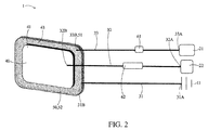
- FIGs. 1 to 3 are schematic views of a wireless communication device according to the first preferred embodiment of the present invention.
- the wireless communication device 1 may be an electronic product capable of wireless communication or a part an electronic product (e.g., a smart phone or a tablet computer or the like) and may transmit data via appropriate communication protocols (e.g., 3G, 4G, 5G, Wi-Fi, BT, and LTE).
- appropriate communication protocols e.g., 3G, 4G, 5G, Wi-Fi, BT, and LTE.
- the wireless communication device 1 may comprise a circuit board 10, a plurality of electronic components 20, a plurality of conducting wires 30, at least one input component 40, an antenna component 50, a back cover 70, a cover glass 90 (as shown in FIG. 8 ) and at least one processor 80.
- the wireless communication device 1 may further comprise one or more signal filters 60 (or called filters).
- the back cover 70 and the cover glass 90 are parts for forming the overall appearance of the wireless communication device 1.
- the back cover 70 may be made of a non-conductor, a conductor or a combination of a conductor and a non-conductor.
- the input component 40 is configured to sense the input of a user and may comprise one of the following components: a capacitive touch-sensing component, a resistive touch-sensing component, an inductive touch-sensing component and an optical touch-sensing component.
- the input component 40 senses the input of the user in combination with the cover glass 90 on a touch-sensing display panel module (not shown).
- the input component 40 is implemented as a capacitive touch-sensing component. The technical contents of those components will be sequentially described as follows.
- the circuit board 10 may be a main circuit board inside the electronic product and may have most of the electronic components 20 disposed thereon. Some mechanical members (e.g., the frame for supporting the touch-sensing display panel module, an electric connector or the like that are not shown in FIG. 1 ) may also be disposed on the circuit board 10.
- the circuit board 10 is generally rectangular in appearance, and the periphery 10A thereof may have a protruding portion or a concave portion. In practical application, the shape of the circuit board 10 is not limited thereto, and the circuit board 10 may also have other shapes.
- the circuit board 10 may comprise a circuit pattern layer (not shown) so that the electronic components 20 can be electrically connected with each other directly or indirectly to transmit electrical signals therebetween.
- the circuit board 10 further comprises one or more ground layers 11 that may be disposed on the outer layer or inner layer (i.e., not exposed to the outside) of the circuit board 10.
- the ground layer 11 may be a metal layer, e.g., a copper foil layer.
- the electronic components 20 may be disposed on the circuit board 10, e.g., via solder or the electric connector (not shown) and may be electrically connected with the circuit pattern layer and/or the ground layer 11 of the circuit board 10.
- the electronic components 20 at least comprise an RF signal module 21 and a touch-sensing signal module 22 that are electrically connected with the processor 80.
- the RF signal module 21 (also known as the RF control module) is configured to receive and transmit an RF signal (also known as the RF microwave signal), and is electrically connected to other electronic components associated with the wireless communication to further process the RF signal via the processor 80, e.g., perform the conversion between the RF signal and the digital signal, power amplification or the like.
- the RF signal module 21 may comprise one or more chips 211 and may also comprise an impedance matching circuit 212.
- the RF signal module 21 may also be integrated into a chip with other electronic components.
- the touch-sensing signal module 22 (also known as the touch-sensing control module) and the processor 80 may be configured to process the touch-sensing signal from the touch-sensing display panel module and the input component (i.e., the capacitive touch-sensing component) 40, e.g., determine the electric capacity of the capacitive touch-sensing component 40 according to the current of the touch-sensing signal, determine whether the capacitive touch-sensing component 40 is touched according to the electric capacity, or the like.
- the touch-sensing signal module 22 may also drive the capacitive touch-sensing component 40.
- the touch-sensing signal module 22 may also be electrically connected with other electronic components to transmit the determination result to the electronic component for further use.
- the touch-sensing signal module 22 may comprise one or more chips and may also be integrated with other electronic components.
- the electronic components 20 may also comprise a memory, a battery, a touch-sensing display panel, various sensors and/or signal processing chips or the like (not shown) to provide various functions for the wireless communication device 1.
- the conducting wires 30 are configured to transmit electrical signals to the circuit board 10, the electronic components 20, the capacitive touch-sensing component 40 and/or the antenna component 50.
- the conducting wires 30 comprise a ground conducting wire 31, a touch-sensing signal conducting wire 32 and an RF signal conducting wire 33.
- Each of the conducting wires 31 to 33 may be a circuit pattern layer printed on the circuit board 10 and/or a metal wire independent of the circuit board 10.
- the independent metal wire may be disposed on a flexible printed circuit substrate (FPCB) 30'.
- the flexible printed circuit substrate 30' may also be electrically connected with the circuit board 10 via a conducting wire 12.
- each of the conducting wires 31 to 33 comprises two opposite ends (i.e., an end 31A and another end 31 B, an end 32A and another end 32B, and an end 33A and another end 33B) in which the electrical signal can be transmitted therebetween.
- the ground conducting wire 31 has an (first) end 31A electrically connected to the ground layer 11 of the circuit board 10 and another (second) end 31 B electrically connected to the capacitive touch-sensing component 40.
- the touch-sensing signal conducting wire 32 has an (first) end 32A electrically connected to the touch-sensing signal module 22 and another (second) end 32B electrically connected to the capacitive touch-sensing component 40.
- the RF signal conducting wire 33 has an (first end) end 33A electrically connected to the RF signal module 21 and another (second) end 33B electrically connected to the antenna component 50.
- the capacitive touch-sensing component 40 may define a capacitance value and may vary the capacitance value in response to the approach of a conductor (e.g., the finger of the user), and then the touch-sensing signal module 22 can sense the variation of the capacitance value to determine whether the capacitive touch-sensing component 40 is touched. In this way, the user can transmit a specific instruction to the wireless communication device 1 by touching the capacitive touch-sensing component 40. As shown in FIG. 1 , the capacitive touch-sensing component 40 may be optionally disposed at the side of the periphery A of the circuit board 10 and be separated from the circuit board 10. The capacitive touch-sensing component 40 may be a key, a scroll bar, a wheel, a pad or the like.
- keys may be classified into physical keys and virtual keys depending on the structural design thereof, and both kinds of keys may each have a specific pattern 100 disposed thereon for the user to identify the function thereof. Both kinds of keys may be combined with the cover glass 90 on the touch-sensing display panel module (not shown) to form an input sensing area 90A for sensing and receiving the input of the user.
- the sensing area 90A is dependent on the position of the input component 40 and is not limited to the fixed position on the cover glass 90.
- the key is defined as the virtual key. If the pattern 100 on a key can be seen no matter whether the display panel module is in the off or on state, then the key is defined as the physical key (in this case, the pattern 100 may be printed on the cover glass 90).
- the electronic components 20 further comprise at least one input component 23 which may also receive the input of the user to communicate with the wireless communication device 1.
- the input component 23 may be a conventional button that is pressed by a user, or may be implemented as a capacitive touch-sensing component, a resistive touch-sensing component, an inductive touch-sensing component or an optical touch-sensing component.
- a biometric identification module (not shown) may also be integrated into the input component 23 to increase the data protection within the wireless communication device 1.
- the cover glass 90 has an opening and the input component 23 is arranged in the opening. Understandably, the input sensing area 90A may be disposed in the peripheral area of the input component 23 to make it convenient for the user to operate.
- the capacitive touch-sensing component 40 may comprise a sensing layer 41, a dielectric layer 42 and a ground layer 43.
- the dielectric layer 42 is disposed between the sensing layer 41 and the ground layer 43.
- the sensing layer 41, the dielectric layer 42 and the ground layer 43 are stacked sequentially.
- the dielectric layer 42 may also surround the sensing layer 41, and the ground layer 43 then surrounds the dielectric layer 42, so the dielectric layer 42 is still disposed between the sensing layer 41 and the ground layer 43.
- the sensing layer 41 may be made of a conductor material (e.g., a metal layer such as a copper foil or an oxide such as indium tin oxide).
- the dielectric layer 42 may be made of a dielectric material (e.g., plastic, resin, glass or the like) or may comprise a hollow portion to use air as the dielectric material.
- the ground layer 43 may be made of a conductor and may further have a mesh structure. In other embodiments, the ground layer 43 may not have a mesh structure.
- the ground layer 43 may be called a second ground layer, while the ground layer 11 of the aforesaid circuit board 10 may be called a first ground layer for distinguishing between the two ground layers.
- the sensing layer 41 may be electrically connected to another end 32B of the touch-sensing signal conducting wire 32.
- the ground layer 43 may be electrically connected to another end 31 B of the ground conducting wire 31.
- the antenna component 50 is configured to receive and/or transmit an RF signal of a specific frequency, and it structurally comprises a feed point 51 and a radiating body 52.
- the feed point 51 is disposed on the ground layer 43 of the capacitive touch-sensing component 40 and is electrically connected to another end 33B of the RF signal conducting wire 33.
- the feed point 51 may be defined as a position at which the other end 33B of the RF signal conducting wire 33 is disposed on the ground layer 43.
- the RF signal is fed into the ground layer 43 via the feed point 51.
- the feed point 51 and the other end 31 B of the ground conducting wire 31 are located at different positions of the ground layer 43 and are spaced apart from each other.
- the radiating body 52 comprises at least a part or all of the ground layer 43 to use the ground layer 43 to receive or transmit electromagnetic waves. That is, the RF signal entering into the ground layer 43 via the feed point 51 will be transmitted in the ground layer 43 and generates an electromagnetic wave. On the other hand, the electromagnetic wave in the environment, when it comes into contact with the ground layer 43, can generate the RF signal in the ground layer 43. Then, the RF signal enters into the RF signal module 21 through the feed point 51 and the RF signal conducting wire 33. Therefore, a part of the ground layer 43 through which the RF signal propagates may be defined as the radiating body 52.
- the RF signal not only radiates in the ground layer 43 but also in the RF signal conducting wire 33 and the ground conducting wire 31, so the RF signal conducting wire 33 and the ground conducting wire 31 may also be regarded as another part comprised in the radiating body 52.
- the total radiating path of the antenna component 50 may be defined starting from an end 33A of the RF signal conducting wire 33, passing through a part of the ground layer 43 and terminating at an end 31A of the ground conducting wire 31.
- the resonance frequency of the radiating body 52 can be changed to obtain the desired frequency.
- the ground conducting wire 31 may also be a part of the radiating body 52, the radiating body 52 as a whole can be viewed as a loop antenna, of which the radiating path corresponds with 1 ⁇ 2 of the wavelength.
- the wireless communication device 1 in this embodiment has the antenna component 50 integrated with the input component (i.e., the capacitive touch-sensing component) 40, and directly uses the ground layer 43 of the capacitive touch-sensing component 40 to receive or transmit the electromagnetic wave.
- the antenna component 50 and the capacitive touch-sensing component 40 can be accommodated in the same space and no additional space is required to accommodate one of the two components, which facilitates the size reduction or space utilization of the wireless communication device 1.
- the wireless communication device 1 in this embodiment may further comprise a plurality of signal filters 60 to reduce or prevent the interference to the RF signal module 21 from the touch-sensing signal, or the interference to the touch-sensing signal module 22 from the RF signal.
- the signal filters 60 (also known as filters) may comprise a touch-sensing signal filter 61 and/or an RF signal filter 62.
- the touch-sensing signal filter 61 may be electrically connected to the RF signal conducting wire 33 in series and has a relatively large impendence for a DC (direct current) or low-frequency touch-sensing signal to block the touch-sensing signal from propagating therethrough. In this way, the touch-sensing signal generated by the capacitive touch-sensing component 40 cannot propagate through the touch-sensing signal filter 61, and thus, cannot enter into the RF signal module 21 through the RF signal conducting wire 33. Therefore, the RF signal module 21 will not be influenced by the touch-sensing signal.
- the touch-sensing signal filter 61 has a relatively small impedance for the highfrequency RF signal, so it will not block the RF signal from passing therethrough. Therefore, the RF signal will not be blocked from passing through the RF signal conducting wire 33 due to the presence of the touch-sensing signal filter 61.
- the touch-sensing signal filter 61 may comprise electronic components such as a capacitor (e.g., a capacitor connected in series), which may present an open-circuited state for the touch-sensing signal, but a short-circuited state for the RF signal.
- the RF signal filter 62 may be electrically connected to the touch-sensing signal conducting wire 32 in series and has a relatively large impendence for a highfrequency RF signal to block the RF signal from propagating therethrough. In this way, the RF signal generated by the antenna component 50 cannot propagate through the RF signal filter 62, and thus, cannot enter into the touch-sensing signal module 22 through the touch-sensing signal conducting wire 32. Therefore, the touch-sensing signal module 22 will not be influenced by the RF signal.
- the RF signal filter 62 has a relatively small impedance for the DC or low-frequency touch-sensing signal, so it will not block the touch-sensing signal from passing therethrough.
- the RF signal filter 62 may comprise electronic components such as an inductor (e.g., an inductor connected in series), which may present an open-circuited state for the RF signal but a short-circuited state for the touch-sensing signal.
- an inductor e.g., an inductor connected in series
- the touch-sensing signal filter 61 and the RF signal filter 62 can increase the reliability of the RF signal module 21 and the touch-sensing signal module 22 respectively.
- the wireless communication device 1 is applied to a mobile phone with a size of 144.6 mm ⁇ 69.7 mm ⁇ 9.61 mm.
- the ground layer 43 has a size of 6 mm ⁇ 17 mm ⁇ 0.1 mm.
- the impedance matching circuit 212 is a ground capacitor connected in parallel (with a capacitance value of 0.8 pF).
- the touch-sensing signal filter 61 is a capacitor with a capacitance value of 1.8 pF
- the RF signal filter 62 is an inductor with an inductance value of 10 nH.
- the measured relationships between the frequency (MHz) and the voltage standing wave ratio (VSWR) are as shown in FIG. 7 , and the relationships between the frequency (MHz) and the efficiency (%) are as shown in the following table.
- the efficiency of each of the frequency bands between the middle frequency (1700 MHz) and the high frequency (2700 MHz) is generally greater than 10%, which means that the wireless communication device 1 has good efficiency in those frequencies and is suitable for use in the carrier aggregation (CA) technology.
- the wireless communication device 1 can operate in a plurality of frequency bands (e.g., B3, B2, B1, B4, B25, B30, B38, B39, B40, B41, B7 and WIFI 2.4G) of the Long-Term Evolution (LTE).
- FIG. 4 illustrates a schematic view of a wireless communication device 2 according to the second preferred embodiment of the present invention.
- the wireless communication device 2 is similar to the aforesaid wireless communication device 1, but the feed point 51 of the antenna component 50 of the wireless communication device 2 may be disposed on the ground layer 43 at a position further from the another end 31 B of the ground conducting wire 31 to increase the radiating path.
- the radiating path can be changed by adjusting the position of the feed point 51 (or the other end 31 B) on the ground layer 43.
- the wireless communication device 2 may further comprise another RF signal filter 63 that is electrically connected to the ground conducting wire 31 to block the RF signal from propagating through the ground conducting wire 31.
- the RF signal filter 63 may comprise electronic components such as an inductor (e.g., an inductor connected in series), which may present an open-circuited state for the RF signal. Therefore, the RF signal entering into the ground layer 43 (the radiating body 52) from the feed point 51 cannot propagate towards the ground layer 11 of the circuit board 10 through the ground conducting wire 31. In this case, it is difficult to use the ground conducting wire 31 as a part of the radiating body 52, so the radiating body 52 as a whole can be viewed as a monopole antenna, of which the radiating path corresponds to 1/4 of the wavelength.
- an inductor e.g., an inductor connected in series
- FIG. 5 is a schematic view of a wireless communication device 3 of the third preferred embodiment of the present invention.
- the wireless communication device 3 mainly differs from the aforesaid wireless communication devices 1 and 2 in that the wireless communication device 3 uses the sensing layer 41 of the capacitive touch-sensing component 40' as the radiating body 52.
- the other end 33B of the RF signal conducting wire 33 is also electrically connected to the sensing layer 41 so that the feed point 51 of the antenna component 50 is disposed on the sensing layer 41.
- the radiating body 52 comprises at least a part of the sensing layer 41.
- the RF signal module 21 may feed the RF signal into the sensing layer 41 via the feed point 51 to generate the electromagnetic wave in the sensing layer 41.
- the electromagnetic wave in the environment can be received by the sensing layer 41 to generate the RF signal.
- the RF signal is then transmitted to the RF signal module 21 via the feed point 51 and the RF signal conducting wire 33.
- the RF signal not only radiates in the sensing layer 41 but also in the RF signal conducting wire 33, so the RF signal conducting wire 33 may also be regarded as another part comprised in the radiating body 52.
- the total radiating path of the antenna component 50 may be defined starting from an end 33A of the RF signal conducting wire 33, passing through a part of the sensing layer 41 and then terminating at the sensing layer 41.
- the wireless communication device 3 may also comprise a touch-sensing signal filter 61 and an RF signal filter 62 to reduce or prevent the interference to the RF signal module 21 from the touch-sensing signal, or the interference to the touch-sensing signal module 22 from the RF signal.
- the antenna component 50 uses the sensing layer 41 of the capacitive touch-sensing component 40' as the radiating body 52, so the capacitive touch-sensing component 40' may not comprise a ground layer without influencing the constitution of the antenna component 50. In other words, even if the capacitive touch-sensing component 40' does not have a ground layer, the antenna component 50 may also be integrated into the capacitive touch-sensing component 40'.
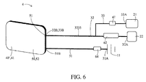
- FIG. 6 is a schematic view of a wireless communication device 4 according to the fourth preferred embodiment of the present invention.
- the wireless communication device 4 and the aforesaid wireless communication device 3 are similar to each other and all use the sensing layer 41 of the capacitive touch-sensing component 40' as the radiating body 52.
- the difference between the aforesaid two wireless communication devices lies in that the RF signal conducting wire 33 and the touch-sensing signal conducting wire 32 of the wireless communication device 4 have a common section 3233.
- the RF signal conducting wire 33 and the touch-sensing signal conducting wire 32 are actually the same conducting wire in the common section 3233 and are two conducting wires outside the common section 3233.
- the other end 33B of the RF signal conducting wire 33 and the other end 32B of the touch-sensing signal conducting wire 32 are disposed on the common section 3233, so the RF signal conducting wire 33 and the touch-sensing signal conducting wire 32 are electrically connected in parallel to the sensing layer 41. In other words, the RF signal conducting wire 33 and the touch-sensing signal conducting wire 32 are electrically connected to the sensing layer at the same position.
- the circuit layout of the wireless communication device 4 can be simplified. If the wireless communication device 4 comprises the touch-sensing signal filter 61 and the RF signal filter 62, then the touch-sensing signal filter 61 and the RF signal filter 62 will be located outside the common section 3233 to prevent the touch-sensing signal or the RF signal from being unable to propagate through the common section 3233. Another difference between the wireless communication device 4 and the wireless communication device 3 lies in that the wireless communication device 4 further comprises a ground conducting wire 31 and another touch-sensing signal filter 64.
- the ground conducting wire 31 has an end 31A electrically connected to the ground layer 11 of the circuit board 10 and the other end 31 B electrically connected to the sensing layer 41 of the capacitive touch-sensing component 40' and spaced apart from the feed point 51.
- the touch-sensing signal filter 64 is electrically connected to the ground conducting wire 31 and may block the touch-sensing signal but allow the RF signal to propagate therethrough. Therefore, the ground conducting wire 31 may be a part of the radiating body 52 so that the antenna component 50 is a loop antenna as a whole.
- the touch-sensing signal filter 64 can block the touch-sensing signal from being transmitted to the ground layer 11 through the ground conducting wire 31, the touch-sensing signal can still be received and processed by the touch-sensing signal module 22.
- the wireless communication devices provided in the embodiments of the present embodiment have an antenna component integrated with at least one input component (e.g., a capacitive touch-sensing component, a resistive touch-sensing component, an inductive touch-sensing component or an optical touch-sensing component), and a sensing layer comprised in the input components.
- the sensing layer may serve as the radiating body of the antenna component, thereby, saving the space occupied by the antenna component.
- the antenna component may further operate at a plurality of frequencies to serve as a diversity antenna that adopts the CA technology.
- the touch-sensing signal will not influence the RF signal module and the RF signal will not influence the touch-sensing signal module, thereby, increasing the operation reliability or the like.
Landscapes
- Engineering & Computer Science (AREA)
- Computer Networks & Wireless Communication (AREA)
- General Engineering & Computer Science (AREA)
- Theoretical Computer Science (AREA)
- Signal Processing (AREA)
- Physics & Mathematics (AREA)
- General Physics & Mathematics (AREA)
- Human Computer Interaction (AREA)
- Electromagnetism (AREA)
- Radar, Positioning & Navigation (AREA)
- Automation & Control Theory (AREA)
- Microelectronics & Electronic Packaging (AREA)
- Support Of Aerials (AREA)
- Transceivers (AREA)
- Telephone Set Structure (AREA)
Abstract
Description
- The present invention provides a wireless communication device, and in particular, it provides a wireless communication device with an antenna component integrated with an input component.
- Wireless communication technology has been widely used in various electronic products. In particular, smart phones and tablet computers use wireless RF (radio frequency) signals of various different frequencies. Therefore, electronic products, such as smart phones and the tablet computers, usually need various antennae to receive and transmit various wireless RF signals.
- However, when the number of antennae increases, the layout of the antennae in electronic products becomes difficult. Researchers have to consider, among other problems, locations where the antennae should be disposed within the electronic products to achieve higher efficiency without occupying the accommodating spaces of other electronic components/modules. Moreover, as electronic products become increasingly thinner, the available space inside the electronic products have become more limited and thus, the layout of the antennae is more difficult.
- Accordingly, a need exists in the art to provide an antenna with desired frequencies in the limited available space within electronic products.
- An objective of the present invention is to provide a wireless communication device which can have an antenna component integrated with an input component (e.g., touch-sensing components such as a capacitive touch-sensing component) to reduce the space required for accommodating the antenna component.
- Another objective of the present invention is to provide another wireless communication device, which can have an antenna component integrated with the input component and prevent mutual interference between signals of the antenna component and input component.
- To achieve the aforesaid objectives, a wireless communication device disclosed in the present invention comprises: a circuit board, comprising a first ground layer; a first input component, comprising a sensing layer, a dielectric layer and a second ground layer, the sensing layer being electrically connected to the first ground layer, the dielectric layer being disposed between the sensing layer and the second ground layer, and the second ground layer being electrically connected to the first ground layer; and an antenna component, comprising a feed point and a radiating body, the feed point being disposed on the second ground layer of the input component, and at least parts of the second ground layer forming a first part of the radiating body.
- To achieve the aforesaid objectives, a wireless communication device disclosed in the present invention comprises: a circuit board, comprising a ground layer; a plurality of electronic components, being disposed on the circuit board and comprising an RF signal module and a touch-sensing signal module; a touch-sensing signal conducting wire and an RF signal conducting wire, an end of the touch-sensing signal conducting wire being electrically connected to the touch-sensing signal module, and an end of the RF signal conducting wire being electrically connected to the RF signal module; a capacitive touch-sensing component, comprising a sensing layer which is electrically connected to another end of the touch-sensing signal conducting wire; and an antenna component, comprising a feed point and a radiating body, the feed point being disposed on the sensing layer of the capacitive touch-sensing component and electrically connected to another end of the RF signal conducting wire, wherein the radiating body comprises at least parts of the sensing layer.
- To achieve the aforesaid objectives, a wireless communication device disclosed in the present invention comprises: a circuit board, comprising a ground layer; a touch-sensing signal conducting wire and an RF signal conducting wire, a first end of the touch-sensing signal conducting wire being electrically connected to the ground layer, and a first end of the RF signal conducting wire being electrically connected to the ground layer; an input component, comprising a sensing layer which is electrically connected to a second end of the touch-sensing signal conducting wire; and an antenna component, comprising a feed point and a radiating body, the feed point being disposed on the sensing layer of the input component, and a second end of the RF signal conducting wire being electrically connected to the sensing layer via the feed point, wherein at least parts of the sensing layer form a first part of the radiating body.
- The aforesaid wireless communication device may further comprise a touch-sensing signal filter and an RF signal filter. The touch-sensing signal filter is electrically connected to the RF signal conducting wire to block the touch-sensing signal from propagating through the RF signal conducting wire. The RF signal filter is electrically connected to the touch-sensing signal conducting wire to block an RF signal from propagating through the touch-sensing signal conducting wire.
- Accordingly, the wireless communication device has at least has the following technical benefits. The radiating body of the antenna component comprises at least a part of the sensing layer or the ground layer of the capacitive touch-sensing component (or other input components), and uses the sensing layer or the ground layer to receive and transmit RF signals, thereby, saving the space required for accommodating the radiating body. In other words, the "sensing layer or the ground layer" and the radiating body share a common space, which prevents the radiating body from occupying the limited space within the device or makes the radiating body occupy less space within the device.
- Additionally, the touch-sensing signal filter can block the touch-sensing signal generated by the capacitive touch-sensing component (or other input components) from entering into the RF signal module, so the touch-sensing signal is unlikely to affect the RF signal module. The RF signal filter can block the RF signal in the antenna component from entering into the touch-sensing signal module, so the RF signal is unlikely to affect the touch-sensing signal module. Therefore, the wireless communication device can be more reliable in performing the touch-sensing and wireless communication functions.
- The detailed technology and preferred embodiments implemented for the subject invention are described in the following paragraphs accompanying the appended drawings for people skilled in this field to well appreciate the features of the claimed invention.
-
-
FIG. 1 is a schematic view of a wireless communication device according to the first preferred embodiment of the present invention; -
FIG. 2 is a schematic view of parts of components inFIG. 1 ; -
FIG. 3 is another schematic view of parts of components inFIG. 1 ; -
FIG. 4 is a schematic view of parts of components of a wireless communication device according to the second preferred embodiment of the present invention; -
FIG. 5 is a schematic view of parts of components of a wireless communication device according to the third preferred embodiment of the present invention; -
FIG. 6 is a schematic view of parts of components of a wireless communication device according to the fourth preferred embodiment of the present invention; -
FIG. 7 is a schematic view illustrating the relationships between the frequency and the voltage standing wave ratio of the wireless communication device according to the first preferred embodiment of the present invention; and -
FIG. 8 is yet another schematic view of parts of components inFIG. 1 . -
FIGs. 1 to 3 are schematic views of a wireless communication device according to the first preferred embodiment of the present invention. Thewireless communication device 1 may be an electronic product capable of wireless communication or a part an electronic product (e.g., a smart phone or a tablet computer or the like) and may transmit data via appropriate communication protocols (e.g., 3G, 4G, 5G, Wi-Fi, BT, and LTE). - The
wireless communication device 1 may comprise acircuit board 10, a plurality ofelectronic components 20, a plurality of conductingwires 30, at least oneinput component 40, an antenna component 50, aback cover 70, a cover glass 90 (as shown inFIG. 8 ) and at least oneprocessor 80. Preferably, thewireless communication device 1 may further comprise one or more signal filters 60 (or called filters). Theback cover 70 and thecover glass 90 are parts for forming the overall appearance of thewireless communication device 1. Theback cover 70 may be made of a non-conductor, a conductor or a combination of a conductor and a non-conductor. - The
input component 40 is configured to sense the input of a user and may comprise one of the following components: a capacitive touch-sensing component, a resistive touch-sensing component, an inductive touch-sensing component and an optical touch-sensing component. Theinput component 40 senses the input of the user in combination with thecover glass 90 on a touch-sensing display panel module (not shown). In this embodiment, theinput component 40 is implemented as a capacitive touch-sensing component. The technical contents of those components will be sequentially described as follows. - As shown in
FIG. 1 , thecircuit board 10 may be a main circuit board inside the electronic product and may have most of theelectronic components 20 disposed thereon. Some mechanical members (e.g., the frame for supporting the touch-sensing display panel module, an electric connector or the like that are not shown inFIG. 1 ) may also be disposed on thecircuit board 10. Thecircuit board 10 is generally rectangular in appearance, and theperiphery 10A thereof may have a protruding portion or a concave portion. In practical application, the shape of thecircuit board 10 is not limited thereto, and thecircuit board 10 may also have other shapes. - Structurally, the
circuit board 10 may comprise a circuit pattern layer (not shown) so that theelectronic components 20 can be electrically connected with each other directly or indirectly to transmit electrical signals therebetween. Thecircuit board 10 further comprises one ormore ground layers 11 that may be disposed on the outer layer or inner layer (i.e., not exposed to the outside) of thecircuit board 10. Theground layer 11 may be a metal layer, e.g., a copper foil layer. Theelectronic components 20 may be disposed on thecircuit board 10, e.g., via solder or the electric connector (not shown) and may be electrically connected with the circuit pattern layer and/or theground layer 11 of thecircuit board 10. Theelectronic components 20 at least comprise anRF signal module 21 and a touch-sensing signal module 22 that are electrically connected with theprocessor 80. The RF signal module 21 (also known as the RF control module) is configured to receive and transmit an RF signal (also known as the RF microwave signal), and is electrically connected to other electronic components associated with the wireless communication to further process the RF signal via theprocessor 80, e.g., perform the conversion between the RF signal and the digital signal, power amplification or the like. TheRF signal module 21 may comprise one ormore chips 211 and may also comprise an impedance matchingcircuit 212. TheRF signal module 21 may also be integrated into a chip with other electronic components. - The touch-sensing signal module 22 (also known as the touch-sensing control module) and the
processor 80 may be configured to process the touch-sensing signal from the touch-sensing display panel module and the input component (i.e., the capacitive touch-sensing component) 40, e.g., determine the electric capacity of the capacitive touch-sensing component 40 according to the current of the touch-sensing signal, determine whether the capacitive touch-sensing component 40 is touched according to the electric capacity, or the like. The touch-sensing signal module 22 may also drive the capacitive touch-sensing component 40. As described above, the touch-sensing signal module 22 may also be electrically connected with other electronic components to transmit the determination result to the electronic component for further use. The touch-sensing signal module 22 may comprise one or more chips and may also be integrated with other electronic components. Depending on the practical applications or requirements, theelectronic components 20 may also comprise a memory, a battery, a touch-sensing display panel, various sensors and/or signal processing chips or the like (not shown) to provide various functions for thewireless communication device 1. - With references to
FIGs. 2 ,3 and8 , the conductingwires 30 are configured to transmit electrical signals to thecircuit board 10, theelectronic components 20, the capacitive touch-sensing component 40 and/or the antenna component 50. The conductingwires 30 comprise a ground conductingwire 31, a touch-sensing signal conductingwire 32 and an RF signal conductingwire 33. Each of the conductingwires 31 to 33 may be a circuit pattern layer printed on thecircuit board 10 and/or a metal wire independent of thecircuit board 10. As shown inFIG. 8 , the independent metal wire may be disposed on a flexible printed circuit substrate (FPCB) 30'. The flexible printed circuit substrate 30' may also be electrically connected with thecircuit board 10 via aconducting wire 12. Structurally, the flexible printed circuit substrate 30' is disposed below thecover glass 90. Additionally, each of the conductingwires 31 to 33 comprises two opposite ends (i.e., anend 31A and anotherend 31 B, anend 32A and anotherend 32B, and anend 33A and anotherend 33B) in which the electrical signal can be transmitted therebetween. Theground conducting wire 31 has an (first)end 31A electrically connected to theground layer 11 of thecircuit board 10 and another (second) end 31 B electrically connected to the capacitive touch-sensingcomponent 40. The touch-sensingsignal conducting wire 32 has an (first)end 32A electrically connected to the touch-sensing signal module 22 and another (second)end 32B electrically connected to the capacitive touch-sensingcomponent 40. The RFsignal conducting wire 33 has an (first end) end 33A electrically connected to theRF signal module 21 and another (second)end 33B electrically connected to the antenna component 50. - The capacitive touch-sensing
component 40 may define a capacitance value and may vary the capacitance value in response to the approach of a conductor (e.g., the finger of the user), and then the touch-sensing signal module 22 can sense the variation of the capacitance value to determine whether the capacitive touch-sensingcomponent 40 is touched. In this way, the user can transmit a specific instruction to thewireless communication device 1 by touching the capacitive touch-sensingcomponent 40. As shown inFIG. 1 , the capacitive touch-sensingcomponent 40 may be optionally disposed at the side of the periphery A of thecircuit board 10 and be separated from thecircuit board 10. The capacitive touch-sensingcomponent 40 may be a key, a scroll bar, a wheel, a pad or the like. - With reference to
FIG. 8 , keys may be classified into physical keys and virtual keys depending on the structural design thereof, and both kinds of keys may each have aspecific pattern 100 disposed thereon for the user to identify the function thereof. Both kinds of keys may be combined with thecover glass 90 on the touch-sensing display panel module (not shown) to form aninput sensing area 90A for sensing and receiving the input of the user. Thesensing area 90A is dependent on the position of theinput component 40 and is not limited to the fixed position on thecover glass 90. - Technically, if the
pattern 100 disposed on the key cannot be seen when the display panel module within the touch-sensing display panel module is in the off state (i.e., when the display is not lit), then the key is defined as the virtual key. If thepattern 100 on a key can be seen no matter whether the display panel module is in the off or on state, then the key is defined as the physical key (in this case, thepattern 100 may be printed on the cover glass 90). - In this embodiment, the
electronic components 20 further comprise at least oneinput component 23 which may also receive the input of the user to communicate with thewireless communication device 1. Theinput component 23 may be a conventional button that is pressed by a user, or may be implemented as a capacitive touch-sensing component, a resistive touch-sensing component, an inductive touch-sensing component or an optical touch-sensing component. Moreover, a biometric identification module (not shown) may also be integrated into theinput component 23 to increase the data protection within thewireless communication device 1. Thecover glass 90 has an opening and theinput component 23 is arranged in the opening. Understandably, theinput sensing area 90A may be disposed in the peripheral area of theinput component 23 to make it convenient for the user to operate. - With reference back to
FIGs. 2 and3 , structurally, the capacitive touch-sensingcomponent 40 may comprise asensing layer 41, adielectric layer 42 and aground layer 43. Thedielectric layer 42 is disposed between thesensing layer 41 and theground layer 43. In other words, thesensing layer 41, thedielectric layer 42 and theground layer 43 are stacked sequentially. In other embodiments, thedielectric layer 42 may also surround thesensing layer 41, and theground layer 43 then surrounds thedielectric layer 42, so thedielectric layer 42 is still disposed between thesensing layer 41 and theground layer 43. - The
sensing layer 41 may be made of a conductor material (e.g., a metal layer such as a copper foil or an oxide such as indium tin oxide). Thedielectric layer 42 may be made of a dielectric material (e.g., plastic, resin, glass or the like) or may comprise a hollow portion to use air as the dielectric material. Theground layer 43 may be made of a conductor and may further have a mesh structure. In other embodiments, theground layer 43 may not have a mesh structure. Theground layer 43 may be called a second ground layer, while theground layer 11 of theaforesaid circuit board 10 may be called a first ground layer for distinguishing between the two ground layers. Thesensing layer 41 may be electrically connected to anotherend 32B of the touch-sensingsignal conducting wire 32. Theground layer 43 may be electrically connected to anotherend 31 B of theground conducting wire 31. Thus, when the capacitance value between thesensing layer 41 and theground layer 43 varies, the corresponding touch-sensing signal can be transmitted to the touch-sensing signal module 22 through the touch-sensingsignal conducting wire 32. - The antenna component 50 is configured to receive and/or transmit an RF signal of a specific frequency, and it structurally comprises a
feed point 51 and a radiating body 52. Thefeed point 51 is disposed on theground layer 43 of the capacitive touch-sensingcomponent 40 and is electrically connected to anotherend 33B of the RFsignal conducting wire 33. In other words, thefeed point 51 may be defined as a position at which theother end 33B of the RFsignal conducting wire 33 is disposed on theground layer 43. The RF signal is fed into theground layer 43 via thefeed point 51. Thefeed point 51 and theother end 31 B of theground conducting wire 31 are located at different positions of theground layer 43 and are spaced apart from each other. - The radiating body 52 comprises at least a part or all of the
ground layer 43 to use theground layer 43 to receive or transmit electromagnetic waves. That is, the RF signal entering into theground layer 43 via thefeed point 51 will be transmitted in theground layer 43 and generates an electromagnetic wave. On the other hand, the electromagnetic wave in the environment, when it comes into contact with theground layer 43, can generate the RF signal in theground layer 43. Then, the RF signal enters into theRF signal module 21 through thefeed point 51 and the RFsignal conducting wire 33. Therefore, a part of theground layer 43 through which the RF signal propagates may be defined as the radiating body 52. The RF signal not only radiates in theground layer 43 but also in the RFsignal conducting wire 33 and theground conducting wire 31, so the RFsignal conducting wire 33 and theground conducting wire 31 may also be regarded as another part comprised in the radiating body 52. Thus, the total radiating path of the antenna component 50 may be defined starting from anend 33A of the RFsignal conducting wire 33, passing through a part of theground layer 43 and terminating at anend 31A of theground conducting wire 31. By adjusting the length of the radiating path (e.g., changing the position of thefeed point 51, changing the length of the RFsignal conducting wire 33 or theground conducting wire 31 or the like), the resonance frequency of the radiating body 52 can be changed to obtain the desired frequency. Additionally, since theground conducting wire 31 may also be a part of the radiating body 52, the radiating body 52 as a whole can be viewed as a loop antenna, of which the radiating path corresponds with ½ of the wavelength. - The
wireless communication device 1 in this embodiment has the antenna component 50 integrated with the input component (i.e., the capacitive touch-sensing component) 40, and directly uses theground layer 43 of the capacitive touch-sensingcomponent 40 to receive or transmit the electromagnetic wave. Thus, the antenna component 50 and the capacitive touch-sensingcomponent 40 can be accommodated in the same space and no additional space is required to accommodate one of the two components, which facilitates the size reduction or space utilization of thewireless communication device 1. - As shown in
FIG. 1 , thewireless communication device 1 in this embodiment may further comprise a plurality of signal filters 60 to reduce or prevent the interference to theRF signal module 21 from the touch-sensing signal, or the interference to the touch-sensing signal module 22 from the RF signal. The signal filters 60 (also known as filters) may comprise a touch-sensing signal filter 61 and/or anRF signal filter 62. - The touch-
sensing signal filter 61 may be electrically connected to the RFsignal conducting wire 33 in series and has a relatively large impendence for a DC (direct current) or low-frequency touch-sensing signal to block the touch-sensing signal from propagating therethrough. In this way, the touch-sensing signal generated by the capacitive touch-sensingcomponent 40 cannot propagate through the touch-sensing signal filter 61, and thus, cannot enter into theRF signal module 21 through the RFsignal conducting wire 33. Therefore, theRF signal module 21 will not be influenced by the touch-sensing signal. - The touch-
sensing signal filter 61 has a relatively small impedance for the highfrequency RF signal, so it will not block the RF signal from passing therethrough. Therefore, the RF signal will not be blocked from passing through the RFsignal conducting wire 33 due to the presence of the touch-sensing signal filter 61. The touch-sensing signal filter 61 may comprise electronic components such as a capacitor (e.g., a capacitor connected in series), which may present an open-circuited state for the touch-sensing signal, but a short-circuited state for the RF signal. - The
RF signal filter 62 may be electrically connected to the touch-sensingsignal conducting wire 32 in series and has a relatively large impendence for a highfrequency RF signal to block the RF signal from propagating therethrough. In this way, the RF signal generated by the antenna component 50 cannot propagate through theRF signal filter 62, and thus, cannot enter into the touch-sensing signal module 22 through the touch-sensingsignal conducting wire 32. Therefore, the touch-sensing signal module 22 will not be influenced by the RF signal. TheRF signal filter 62 has a relatively small impedance for the DC or low-frequency touch-sensing signal, so it will not block the touch-sensing signal from passing therethrough. Therefore, the touch-sensing signal will not be blocked from passing through the touch-sensingsignal conducting wire 32 due to the presence of theRF signal filter 62. TheRF signal filter 62 may comprise electronic components such as an inductor (e.g., an inductor connected in series), which may present an open-circuited state for the RF signal but a short-circuited state for the touch-sensing signal. - The touch-
sensing signal filter 61 and theRF signal filter 62 can increase the reliability of theRF signal module 21 and the touch-sensing signal module 22 respectively. As an example of a practical test, thewireless communication device 1 is applied to a mobile phone with a size of 144.6 mm × 69.7 mm × 9.61 mm. Theground layer 43 has a size of 6 mm × 17 mm × 0.1 mm. Theimpedance matching circuit 212 is a ground capacitor connected in parallel (with a capacitance value of 0.8 pF). The touch-sensing signal filter 61 is a capacitor with a capacitance value of 1.8 pF, and theRF signal filter 62 is an inductor with an inductance value of 10 nH. The measured relationships between the frequency (MHz) and the voltage standing wave ratio (VSWR) are as shown inFIG. 7 , and the relationships between the frequency (MHz) and the efficiency (%) are as shown in the following table.Frequency 1710.2 1747.8 1784.8 1805.2 1850.2 1880 1909.8 1930.2 Efficiency 11.19 11.87 12.05 12.27 13.06 15.60 16.63 17.95 Frequency 1960 1989.8 2010 2025 2110 2140 2167.6 2300.8 Efficiency 17.92 17.74 17.04 16.81 15.48 15.32 16.16 17.85 Frequency 2350 2399.2 2500 2540 2580 2610 2650 2690 Efficiency 16.27 17.07 13.77 14.11 11.97 10.33 11.56 9.95 - The efficiency of each of the frequency bands between the middle frequency (1700 MHz) and the high frequency (2700 MHz) is generally greater than 10%, which means that the
wireless communication device 1 has good efficiency in those frequencies and is suitable for use in the carrier aggregation (CA) technology. Thus, thewireless communication device 1 can operate in a plurality of frequency bands (e.g., B3, B2, B1, B4, B25, B30, B38, B39, B40, B41, B7 and WIFI 2.4G) of the Long-Term Evolution (LTE). - What is described above is the technical content of the
wireless communication device 1, and the technical content of thewireless communication device 1 according to other embodiments of the present invention will be described hereinafter. Cross-references may be made between technical contents of thewireless communication device 1 of different embodiments, so identical descriptions will be omitted or simplified. -
FIG. 4 illustrates a schematic view of awireless communication device 2 according to the second preferred embodiment of the present invention. Thewireless communication device 2 is similar to the aforesaidwireless communication device 1, but thefeed point 51 of the antenna component 50 of thewireless communication device 2 may be disposed on theground layer 43 at a position further from the anotherend 31 B of theground conducting wire 31 to increase the radiating path. The radiating path can be changed by adjusting the position of the feed point 51 (or theother end 31 B) on theground layer 43. Additionally, thewireless communication device 2 may further comprise anotherRF signal filter 63 that is electrically connected to theground conducting wire 31 to block the RF signal from propagating through theground conducting wire 31. TheRF signal filter 63 may comprise electronic components such as an inductor (e.g., an inductor connected in series), which may present an open-circuited state for the RF signal. Therefore, the RF signal entering into the ground layer 43 (the radiating body 52) from thefeed point 51 cannot propagate towards theground layer 11 of thecircuit board 10 through theground conducting wire 31.
In this case, it is difficult to use theground conducting wire 31 as a part of the radiating body 52, so the radiating body 52 as a whole can be viewed as a monopole antenna, of which the radiating path corresponds to 1/4 of the wavelength. -
FIG. 5 is a schematic view of awireless communication device 3 of the third preferred embodiment of the present invention. Thewireless communication device 3 mainly differs from the aforesaidwireless communication devices wireless communication device 3 uses thesensing layer 41 of the capacitive touch-sensing component 40' as the radiating body 52. - Particularly, in the
wireless communication device 3, in addition to theother end 32B of the touch-sensingsignal conducting wire 32, theother end 33B of the RFsignal conducting wire 33 is also electrically connected to thesensing layer 41 so that thefeed point 51 of the antenna component 50 is disposed on thesensing layer 41. The radiating body 52 comprises at least a part of thesensing layer 41. In this way, theRF signal module 21 may feed the RF signal into thesensing layer 41 via thefeed point 51 to generate the electromagnetic wave in thesensing layer 41. Alternatively, the electromagnetic wave in the environment can be received by thesensing layer 41 to generate the RF signal. The RF signal is then transmitted to theRF signal module 21 via thefeed point 51 and the RFsignal conducting wire 33. Similarly, the RF signal not only radiates in thesensing layer 41 but also in the RFsignal conducting wire 33, so the RFsignal conducting wire 33 may also be regarded as another part comprised in the radiating body 52. Thus, the total radiating path of the antenna component 50 may be defined starting from anend 33A of the RFsignal conducting wire 33, passing through a part of thesensing layer 41 and then terminating at thesensing layer 41. - As shown in
FIG. 1 , since the sensing layer 41 (the radiating body 52) is not electrically connected to theground layer 11 of thecircuit board 10, the RF signal in thesensing layer 41 will not be transmitted towards theground layer 11 of thecircuit board 10. Therefore, the radiating body 52 as a whole can be viewed as a monopole antenna, of which the radiating path corresponds to 1/4 of the wavelength. Thewireless communication device 3 may also comprise a touch-sensing signal filter 61 and anRF signal filter 62 to reduce or prevent the interference to theRF signal module 21 from the touch-sensing signal, or the interference to the touch-sensing signal module 22 from the RF signal. - It shall be additionally appreciated that the antenna component 50 uses the
sensing layer 41 of the capacitive touch-sensing component 40' as the radiating body 52, so the capacitive touch-sensing component 40' may not comprise a ground layer without influencing the constitution of the antenna component 50. In other words, even if the capacitive touch-sensing component 40' does not have a ground layer, the antenna component 50 may also be integrated into the capacitive touch-sensing component 40'. -
FIG. 6 is a schematic view of awireless communication device 4 according to the fourth preferred embodiment of the present invention. Thewireless communication device 4 and the aforesaidwireless communication device 3 are similar to each other and all use thesensing layer 41 of the capacitive touch-sensing component 40' as the radiating body 52. The difference between the aforesaid two wireless communication devices lies in that the RFsignal conducting wire 33 and the touch-sensingsignal conducting wire 32 of thewireless communication device 4 have acommon section 3233. The RFsignal conducting wire 33 and the touch-sensingsignal conducting wire 32 are actually the same conducting wire in thecommon section 3233 and are two conducting wires outside thecommon section 3233. Theother end 33B of the RFsignal conducting wire 33 and theother end 32B of the touch-sensingsignal conducting wire 32 are disposed on thecommon section 3233, so the RFsignal conducting wire 33 and the touch-sensingsignal conducting wire 32 are electrically connected in parallel to thesensing layer 41. In other words, the RFsignal conducting wire 33 and the touch-sensingsignal conducting wire 32 are electrically connected to the sensing layer at the same position. - Due to the arrangement of the
common section 3233, the circuit layout of thewireless communication device 4 can be simplified. If thewireless communication device 4 comprises the touch-sensing signal filter 61 and theRF signal filter 62, then the touch-sensing signal filter 61 and theRF signal filter 62 will be located outside thecommon section 3233 to prevent the touch-sensing signal or the RF signal from being unable to propagate through thecommon section 3233.
Another difference between thewireless communication device 4 and thewireless communication device 3 lies in that thewireless communication device 4 further comprises aground conducting wire 31 and another touch-sensing signal filter 64. Theground conducting wire 31 has anend 31A electrically connected to theground layer 11 of thecircuit board 10 and theother end 31 B electrically connected to thesensing layer 41 of the capacitive touch-sensing component 40' and spaced apart from thefeed point 51. The touch-sensing signal filter 64 is electrically connected to theground conducting wire 31 and may block the touch-sensing signal but allow the RF signal to propagate therethrough. Therefore, theground conducting wire 31 may be a part of the radiating body 52 so that the antenna component 50 is a loop antenna as a whole. Moreover, since the touch-sensing signal filter 64 can block the touch-sensing signal from being transmitted to theground layer 11 through theground conducting wire 31, the touch-sensing signal can still be received and processed by the touch-sensing signal module 22. - The wireless communication devices provided in the embodiments of the present embodiment have an antenna component integrated with at least one input component (e.g., a capacitive touch-sensing component, a resistive touch-sensing component, an inductive touch-sensing component or an optical touch-sensing component), and a sensing layer comprised in the input components. The sensing layer may serve as the radiating body of the antenna component, thereby, saving the space occupied by the antenna component. Additionally, the antenna component may further operate at a plurality of frequencies to serve as a diversity antenna that adopts the CA technology. Moreover, due to the arrangement of the signal filters, the touch-sensing signal will not influence the RF signal module and the RF signal will not influence the touch-sensing signal module, thereby, increasing the operation reliability or the like.
- It will be apparent to those skilled in the art that various modifications and variations may be made to the structure of the disclosed embodiments without departing from the scope of the disclosure.
Claims (15)
- A wireless communication device, comprising:a circuit board (10), comprising a first ground layer;a first input component (40), comprising a sensing layer (41), a dielectric layer (42) and a second ground layer, wherein the sensing layer (41) is electrically connected to the first ground layer, the dielectric layer (42) is disposed between the sensing layer (41) and the second ground layer, and the second ground layer is electrically connected to the first ground layer; andan antenna component (50), comprising a feed point (51) and a radiating body (52), the feed point (51) is disposed on the second ground layer of the first input component, and at least parts of the second ground layer forms a first part of the radiating body.
- The wireless communication device of claim 1, further comprising a ground conducting wire having a first end electrically connected to the first ground layer and a second end electrically connected to the second ground layer.
- The wireless communication device of claim 2, further comprising a radio frequency (RF) signal conducting wire having a first end electrically connected to the first ground layer and a second end electrically connected to the second ground layer, preferably wherein the ground conducting wire and the RF signal conducting wire form a second part of the radiating body.
- The wireless communication device of claim 3, further comprising:an RF signal module (21) and a touch-sensing signal module (22), both are disposed on the circuit board (10); anda touch-sensing signal conducting wire having a first end electrically connected to the touch-sensing signal module (22) and a second end electrically connected to the sensing layer (41), and the first end of the RF signal conducting wire is electrically connected to the RF signal module (21), preferably wherein the touch-sensing signal conducting wire and the RF signal conducting wire are disposed on one of the circuit board and a flexible printed circuit substrate.
- The wireless communication device of according to any one of preceding claims, further comprising:a cover glass (90), wherein an input sensing area (90A) is formed by the first input component (40) on the cover glass (90).
- The wireless communication device of claim 5, wherein the first input component (40) comprises one of a capacitive touch-sensing component, a resistive touch-sensing component, an inductive touch-sensing component and an optical touch-sensing component; and a second input component, wherein the cover glass (90) has an opening and the second input component is arranged into the opening.
- The wireless communication device of claim 5, wherein the input sensing area is disposed in a surrounding area of the second input component, and wherein the second input component comprises a biometirc identification module.
- The wireless communication device according to any one of preceding claims, further comprising an RF signal filter, wherein the RF signal filter is electrically connected to the touch-sensing signal conducting wire to block an RF signal from propagating through the touch-sensing signal conducting wire, preferably wherein the RF signal filter comprises an inductor.
- The wireless communication device according to any one of preceding claims, further comprising an RF signal filter, wherein the RF signal filter is electrically connected to the ground conducting wire to block an RF signal from propagating through the ground conducting wire, preferably wherein the RF signal filter comprises an inductor.
- The wireless communication device of claim 3, further comprising a touch-sensing signal filter, wherein the touch-sensing signal filter is electrically connected to the RF signal conducting wire to block an RF signal from propagating through the RF signal conducting wire, preferably wherein the touch-sensing signal filter comprises a capacitor.
- A wireless communication device, comprising:a circuit board (10), comprising a ground layer;a touch-sensing signal conducting wire and an RF signal conducting wire, a first end of the touch-sensing signal conducting wire and a first end of the RF signal conducting wire are electrically connected to the ground layer;an input component, comprising a sensing layer (41) which is electrically connected to a second end of the touch-sensing signal conducting wire; andan antenna component (50), comprising a feed point and a radiating body, the feed point being disposed on the sensing layer of the input component, and a second end of the RF signal conducting wire being electrically connected to the sensing layer via the feed point, wherein at least parts of the sensing layer form a first part of the radiating body.
- The wireless communication device of claim 11, wherein the input component comprises one of a capacitive touch-sensing component, a resistive touch-sensing component, an inductive touch-sensing component and an optical touch-sensing component.
- The wireless communication device of claim 11, further comprising a touch-sensing signal filter and an RF signal filter, wherein the touch-sensing signal filter is electrically connected to the RF signal conducting wire to block a touch-sensing signal from propagating through the RF signal conducting wire; and the RF signal filter is electrically connected to the touch-sensing signal conducting wire to block an RF signal from propagating through the touch-sensing signal conducting wire, preferably
wherein the touch-sensing signal filter comprises a capacitor, and the RF signal filter comprises an inductor. - The wireless communication device of claims 11 to 13, wherein a second end of the touch-sensing signal conducting wire and a second end of the RF signal conducting wire are electrically connected in parallel to the sensing layer.
- The wireless communication device of claims 11 to 14, further comprising a ground conducting wire having a first end electrically connected to the ground layer and a second end electrically connected to the sensing layer, preferably wherein the ground conducting wire and the RF signal conducting wire form a second part of the radiating body.
Applications Claiming Priority (1)
| Application Number | Priority Date | Filing Date | Title |
|---|---|---|---|
| US15/094,684 US9628115B1 (en) | 2016-04-08 | 2016-04-08 | Wireless communication device |
Publications (2)
| Publication Number | Publication Date |
|---|---|
| EP3229315A1 true EP3229315A1 (en) | 2017-10-11 |
| EP3229315B1 EP3229315B1 (en) | 2020-11-25 |
Family
ID=57130253
Family Applications (1)
| Application Number | Title | Priority Date | Filing Date |
|---|---|---|---|
| EP16193434.4A Active EP3229315B1 (en) | 2016-04-08 | 2016-10-12 | Wireless communication device integrating touch-sensing component with antenna |
Country Status (4)
| Country | Link |
|---|---|
| US (2) | US9628115B1 (en) |
| EP (1) | EP3229315B1 (en) |
| CN (2) | CN111697318B (en) |
| TW (1) | TWI621304B (en) |
Families Citing this family (16)
| Publication number | Priority date | Publication date | Assignee | Title |
|---|---|---|---|---|
| CN109429516B (en) * | 2017-06-22 | 2021-12-24 | 京东方科技集团股份有限公司 | Touch substrate, touch display device and method of manufacturing touch substrate |
| CN107492716B (en) * | 2017-07-31 | 2020-08-14 | Oppo广东移动通信有限公司 | Control method, antenna device and electronic device |
| TWM575942U (en) * | 2018-08-02 | 2019-03-21 | 禾伸堂企業股份有限公司 | Bluetooth earphone combined with antenna and touch sensor |
| US20200068456A1 (en) * | 2018-08-27 | 2020-02-27 | T-Mobile Usa, Inc. | Displaying network availability in dual connectivity networks |
| KR102526400B1 (en) | 2018-09-06 | 2023-04-28 | 삼성전자주식회사 | An electronic device comprising a 5g antenna module |
| US11050452B2 (en) * | 2018-12-06 | 2021-06-29 | Apple Inc. | Electronic devices having circuitry in housing attachment structures |
| KR102996312B1 (en) * | 2019-01-07 | 2026-07-27 | 삼성전자주식회사 | Method for controlling power back off using grip sensor and electronic device for supporting the same |
| CN113454582B (en) * | 2019-01-10 | 2023-01-17 | 万魔声学股份有限公司 | Multiplexing structure of wireless antenna and touch sensor touch panel and wireless wearable device |
| US11116030B2 (en) * | 2019-04-29 | 2021-09-07 | T-Mobile Usa, Inc. | 5G wireless network connection symbol policy |
| US11513630B2 (en) * | 2019-08-27 | 2022-11-29 | Samsung Electro-Mechanics Co., Ltd. | Touch operation sensing device using impedance change caused by touch operation |
| USD913625S1 (en) * | 2019-10-01 | 2021-03-16 | Y.Share S.R.L. | Key case |
| US11102627B1 (en) | 2020-02-14 | 2021-08-24 | T-Mobile Usa, Inc. | Service type symbols |
| US11382106B2 (en) | 2020-04-22 | 2022-07-05 | T-Mobile Usa, Inc. | Network symbol display for dual connectivity networks |
| CN112738679A (en) * | 2020-12-24 | 2021-04-30 | Oppo广东移动通信有限公司 | Signal receiving and transmitting device, electronic equipment, wearable equipment and wireless earphone |
| CN115704919B (en) * | 2021-08-03 | 2026-03-10 | 南京矽力微电子(香港)有限公司 | Mobile device |
| CN114094330B (en) * | 2021-11-24 | 2025-01-21 | 歌尔科技有限公司 | A device and antenna thereof |
Citations (3)
| Publication number | Priority date | Publication date | Assignee | Title |
|---|---|---|---|---|
| US20040183788A1 (en) * | 2003-01-30 | 2004-09-23 | Fujitsu Component Limited | Touch panel, and input device and electronic apparatus each equipped with the touch panel |
| US20120034888A1 (en) * | 2010-08-05 | 2012-02-09 | Franco De Flaviis | Method and System for Utilizing a Touchscreen Interface as an Antenna |
| US20140087786A1 (en) * | 2012-09-26 | 2014-03-27 | Panasonic Corporation | Communication equipment and electronic equipment |
Family Cites Families (18)
| Publication number | Priority date | Publication date | Assignee | Title |
|---|---|---|---|---|
| US5661493A (en) * | 1994-12-02 | 1997-08-26 | Spar Aerospace Limited | Layered dual frequency antenna array |
| US6747600B2 (en) * | 2002-05-08 | 2004-06-08 | Accton Technology Corporation | Dual-band monopole antenna |
| TW557604B (en) * | 2002-05-23 | 2003-10-11 | Realtek Semiconductor Corp | Printed antenna structure |
| US8577289B2 (en) * | 2011-02-17 | 2013-11-05 | Apple Inc. | Antenna with integrated proximity sensor for proximity-based radio-frequency power control |
| CN102163112B (en) * | 2011-04-07 | 2014-07-23 | 台均科技(深圳)有限公司 | Sensor, dual-mode touch module and dual-mode touch electronic device |
| CN103051320A (en) * | 2011-10-14 | 2013-04-17 | 十速兴业科技(深圳)有限公司 | Circuit layout of touch button and detection method thereof |
| US8933902B2 (en) * | 2012-08-13 | 2015-01-13 | Htc Corporation | Touch panel structure, touch and display panel structure, and integrated touch display panel structure having antenna pattern and method of forming touch panel having antenna pattern |
| CN203084702U (en) * | 2012-09-17 | 2013-07-24 | 太瀚科技股份有限公司 | Electromagnetic induction antenna substrate, composite substrate, electromagnetic input device and device with touch and writing input functions |
| CN103682566A (en) * | 2012-09-26 | 2014-03-26 | 国基电子(上海)有限公司 | Communication device |
| US9065175B2 (en) * | 2012-10-18 | 2015-06-23 | Apple Inc. | Antenna structures and electrical components with grounding |
| US9179537B2 (en) * | 2012-12-13 | 2015-11-03 | Apple Inc. | Methods for forming metallized dielectric structures |
| KR102046564B1 (en) * | 2013-02-07 | 2019-11-20 | 삼성디스플레이 주식회사 | Touch Screen Panel Having Antenna Pattern and Display Device Having the Same |
| US9024826B2 (en) * | 2013-02-25 | 2015-05-05 | Htc Corporation | Electronic devices with antennas formed with optically-transparent films and related methods |
| TWI497825B (en) * | 2013-04-19 | 2015-08-21 | Wistron Neweb Corp | Radio-frequency device and wireless communication device |
| CN104467897B (en) * | 2013-09-25 | 2017-06-06 | 宏碁股份有限公司 | Mobile device |
| KR102174679B1 (en) * | 2013-12-31 | 2020-11-06 | 엘지디스플레이 주식회사 | Touch panel |
| US9356661B2 (en) * | 2014-04-23 | 2016-05-31 | Apple Inc. | Electronic device with near-field antenna operating through display |
| US9793599B2 (en) * | 2015-03-06 | 2017-10-17 | Apple Inc. | Portable electronic device with antenna |
-
2016
- 2016-04-08 US US15/094,684 patent/US9628115B1/en active Active
- 2016-07-20 TW TW105122871A patent/TWI621304B/en active
- 2016-07-26 CN CN202010573556.5A patent/CN111697318B/en active Active
- 2016-07-26 CN CN201610592500.8A patent/CN107293841B/en active Active
- 2016-10-12 EP EP16193434.4A patent/EP3229315B1/en active Active
-
2017
- 2017-03-20 US US15/463,974 patent/US10122837B2/en active Active
Patent Citations (3)
| Publication number | Priority date | Publication date | Assignee | Title |
|---|---|---|---|---|
| US20040183788A1 (en) * | 2003-01-30 | 2004-09-23 | Fujitsu Component Limited | Touch panel, and input device and electronic apparatus each equipped with the touch panel |
| US20120034888A1 (en) * | 2010-08-05 | 2012-02-09 | Franco De Flaviis | Method and System for Utilizing a Touchscreen Interface as an Antenna |
| US20140087786A1 (en) * | 2012-09-26 | 2014-03-27 | Panasonic Corporation | Communication equipment and electronic equipment |
Non-Patent Citations (1)
| Title |
|---|
| MATTHAEI G L ET AL: "Microwave filters, impedance matching networks, and coupling structures, Some general applications of filter structures in microwave engineering, Multiplexer design", 1 January 1980, MICROWAVE FILTERS, IMPEDANCE-MATCHING NETWORKS AND COUPLING STRUCTURES, ARTECH HOUSE BOOKS, DEDHAM, MA, US, PAGE(S) 1 - 3,965, ISBN: 978-0-89006-099-5, XP002513077 * |
Also Published As
| Publication number | Publication date |
|---|---|
| CN107293841B (en) | 2020-07-17 |
| TW201737552A (en) | 2017-10-16 |
| TWI621304B (en) | 2018-04-11 |
| US10122837B2 (en) | 2018-11-06 |
| CN111697318A (en) | 2020-09-22 |
| US20170244819A1 (en) | 2017-08-24 |
| EP3229315B1 (en) | 2020-11-25 |
| CN111697318B (en) | 2022-02-25 |
| CN107293841A (en) | 2017-10-24 |
| US9628115B1 (en) | 2017-04-18 |
| US20180183914A9 (en) | 2018-06-28 |
Similar Documents
| Publication | Publication Date | Title |
|---|---|---|
| EP3229315B1 (en) | Wireless communication device integrating touch-sensing component with antenna | |
| CN202025842U (en) | Parallel feeding loop antenna, electronic device and radio circuit | |
| CN105940548B (en) | Electronic device with slot antenna and proximity sensor | |
| AU2010273846B2 (en) | Electronic devices with capacitive proximity sensors for proximity-based radio-frequency power control | |
| US20190288376A1 (en) | Mobile device and antenna structure | |
| US20120133597A1 (en) | Antenna structure | |
| US9674321B2 (en) | Mobile terminal antenna module housed within metal rear cover serving as a radiator | |
| WO2017162136A1 (en) | Antenna apparatus, metal housing and mobile terminal | |
| TWI853429B (en) | Electronic device and antenna structure | |
| CN103972646A (en) | Antenna arrangement | |
| TWI549369B (en) | Communication device | |
| CN104795625A (en) | Antenna structure with distance sensor | |
| CN105514571B (en) | Antenna device and electronic apparatus | |
| TWI827309B (en) | Antenna module and electronic device | |
| US10340590B2 (en) | Device assembly applied to mobile terminal and mobile terminal | |
| CN112952344B (en) | Electronic equipment | |
| TWM484801U (en) | Antenna structure with proximity sensor | |
| CN104124513A (en) | communication device | |
| CN109004343A (en) | Antenna assembly and electronic equipment | |
| CN118693506A (en) | Electronic device and antenna structure | |
| US20150244058A1 (en) | Electronic Device Having Antenna Module | |
| CN214706226U (en) | Mobile terminal | |
| TWI629833B (en) | Terminal device having hybrid antenna integrating with capacitive proximity sensors | |
| CN115704919B (en) | Mobile device | |
| CN206878155U (en) | Miniaturized intelligent module with antenna interface |
Legal Events
| Date | Code | Title | Description |
|---|---|---|---|
| PUAI | Public reference made under article 153(3) epc to a published international application that has entered the european phase |
Free format text: ORIGINAL CODE: 0009012 |
|
| STAA | Information on the status of an ep patent application or granted ep patent |
Free format text: STATUS: REQUEST FOR EXAMINATION WAS MADE |
|
| 17P | Request for examination filed |
Effective date: 20161012 |
|
| AK | Designated contracting states |
Kind code of ref document: A1 Designated state(s): AL AT BE BG CH CY CZ DE DK EE ES FI FR GB GR HR HU IE IS IT LI LT LU LV MC MK MT NL NO PL PT RO RS SE SI SK SM TR |
|
| AX | Request for extension of the european patent |
Extension state: BA ME |
|
| RBV | Designated contracting states (corrected) |
Designated state(s): AL AT BE BG CH CY CZ DE DK EE ES FI FR GB GR HR HU IE IS IT LI LT LU LV MC MK MT NL NO PL PT RO RS SE SI SK SM TR |
|
| STAA | Information on the status of an ep patent application or granted ep patent |
Free format text: STATUS: EXAMINATION IS IN PROGRESS |
|
| R17P | Request for examination filed (corrected) |
Effective date: 20161012 |
|
| 17Q | First examination report despatched |
Effective date: 20200226 |
|
| REG | Reference to a national code |
Ref country code: DE Ref legal event code: R079 Ref document number: 602016048453 Country of ref document: DE Free format text: PREVIOUS MAIN CLASS: H01Q0001240000 Ipc: H01Q0001220000 |
|
| GRAP | Despatch of communication of intention to grant a patent |
Free format text: ORIGINAL CODE: EPIDOSNIGR1 |
|
| STAA | Information on the status of an ep patent application or granted ep patent |
Free format text: STATUS: GRANT OF PATENT IS INTENDED |
|
| RIC1 | Information provided on ipc code assigned before grant |
Ipc: H01Q 1/44 20060101ALI20200416BHEP Ipc: H01Q 1/24 20060101ALI20200416BHEP Ipc: H01Q 1/22 20060101AFI20200416BHEP Ipc: G06F 3/044 20060101ALI20200416BHEP |
|
| INTG | Intention to grant announced |
Effective date: 20200519 |
|
| GRAS | Grant fee paid |
Free format text: ORIGINAL CODE: EPIDOSNIGR3 |
|
| GRAA | (expected) grant |
Free format text: ORIGINAL CODE: 0009210 |
|
| STAA | Information on the status of an ep patent application or granted ep patent |
Free format text: STATUS: THE PATENT HAS BEEN GRANTED |
|
| AK | Designated contracting states |
Kind code of ref document: B1 Designated state(s): AL AT BE BG CH CY CZ DE DK EE ES FI FR GB GR HR HU IE IS IT LI LT LU LV MC MK MT NL NO PL PT RO RS SE SI SK SM TR |
|
| REG | Reference to a national code |
Ref country code: GB Ref legal event code: FG4D |
|
| REG | Reference to a national code |
Ref country code: CH Ref legal event code: EP |
|
| REG | Reference to a national code |
Ref country code: AT Ref legal event code: REF Ref document number: 1339344 Country of ref document: AT Kind code of ref document: T Effective date: 20201215 |
|
| REG | Reference to a national code |
Ref country code: DE Ref legal event code: R096 Ref document number: 602016048453 Country of ref document: DE |
|
| REG | Reference to a national code |
Ref country code: IE Ref legal event code: FG4D |
|
| REG | Reference to a national code |
Ref country code: NL Ref legal event code: FP |
|
| REG | Reference to a national code |
Ref country code: AT Ref legal event code: MK05 Ref document number: 1339344 Country of ref document: AT Kind code of ref document: T Effective date: 20201125 |
|
| PG25 | Lapsed in a contracting state [announced via postgrant information from national office to epo] |
Ref country code: RS Free format text: LAPSE BECAUSE OF FAILURE TO SUBMIT A TRANSLATION OF THE DESCRIPTION OR TO PAY THE FEE WITHIN THE PRESCRIBED TIME-LIMIT Effective date: 20201125 Ref country code: PT Free format text: LAPSE BECAUSE OF FAILURE TO SUBMIT A TRANSLATION OF THE DESCRIPTION OR TO PAY THE FEE WITHIN THE PRESCRIBED TIME-LIMIT Effective date: 20210325 Ref country code: NO Free format text: LAPSE BECAUSE OF FAILURE TO SUBMIT A TRANSLATION OF THE DESCRIPTION OR TO PAY THE FEE WITHIN THE PRESCRIBED TIME-LIMIT Effective date: 20210225 Ref country code: FI Free format text: LAPSE BECAUSE OF FAILURE TO SUBMIT A TRANSLATION OF THE DESCRIPTION OR TO PAY THE FEE WITHIN THE PRESCRIBED TIME-LIMIT Effective date: 20201125 Ref country code: GR Free format text: LAPSE BECAUSE OF FAILURE TO SUBMIT A TRANSLATION OF THE DESCRIPTION OR TO PAY THE FEE WITHIN THE PRESCRIBED TIME-LIMIT Effective date: 20210226 |
|
| PG25 | Lapsed in a contracting state [announced via postgrant information from national office to epo] |
Ref country code: AT Free format text: LAPSE BECAUSE OF FAILURE TO SUBMIT A TRANSLATION OF THE DESCRIPTION OR TO PAY THE FEE WITHIN THE PRESCRIBED TIME-LIMIT Effective date: 20201125 Ref country code: LV Free format text: LAPSE BECAUSE OF FAILURE TO SUBMIT A TRANSLATION OF THE DESCRIPTION OR TO PAY THE FEE WITHIN THE PRESCRIBED TIME-LIMIT Effective date: 20201125 Ref country code: PL Free format text: LAPSE BECAUSE OF FAILURE TO SUBMIT A TRANSLATION OF THE DESCRIPTION OR TO PAY THE FEE WITHIN THE PRESCRIBED TIME-LIMIT Effective date: 20201125 Ref country code: IS Free format text: LAPSE BECAUSE OF FAILURE TO SUBMIT A TRANSLATION OF THE DESCRIPTION OR TO PAY THE FEE WITHIN THE PRESCRIBED TIME-LIMIT Effective date: 20210325 Ref country code: BG Free format text: LAPSE BECAUSE OF FAILURE TO SUBMIT A TRANSLATION OF THE DESCRIPTION OR TO PAY THE FEE WITHIN THE PRESCRIBED TIME-LIMIT Effective date: 20210225 Ref country code: SE Free format text: LAPSE BECAUSE OF FAILURE TO SUBMIT A TRANSLATION OF THE DESCRIPTION OR TO PAY THE FEE WITHIN THE PRESCRIBED TIME-LIMIT Effective date: 20201125 |
|
| REG | Reference to a national code |
Ref country code: LT Ref legal event code: MG9D |
|
| PG25 | Lapsed in a contracting state [announced via postgrant information from national office to epo] |
Ref country code: HR Free format text: LAPSE BECAUSE OF FAILURE TO SUBMIT A TRANSLATION OF THE DESCRIPTION OR TO PAY THE FEE WITHIN THE PRESCRIBED TIME-LIMIT Effective date: 20201125 |
|
| PG25 | Lapsed in a contracting state [announced via postgrant information from national office to epo] |
Ref country code: RO Free format text: LAPSE BECAUSE OF FAILURE TO SUBMIT A TRANSLATION OF THE DESCRIPTION OR TO PAY THE FEE WITHIN THE PRESCRIBED TIME-LIMIT Effective date: 20201125 Ref country code: SK Free format text: LAPSE BECAUSE OF FAILURE TO SUBMIT A TRANSLATION OF THE DESCRIPTION OR TO PAY THE FEE WITHIN THE PRESCRIBED TIME-LIMIT Effective date: 20201125 Ref country code: LT Free format text: LAPSE BECAUSE OF FAILURE TO SUBMIT A TRANSLATION OF THE DESCRIPTION OR TO PAY THE FEE WITHIN THE PRESCRIBED TIME-LIMIT Effective date: 20201125 Ref country code: SM Free format text: LAPSE BECAUSE OF FAILURE TO SUBMIT A TRANSLATION OF THE DESCRIPTION OR TO PAY THE FEE WITHIN THE PRESCRIBED TIME-LIMIT Effective date: 20201125 Ref country code: EE Free format text: LAPSE BECAUSE OF FAILURE TO SUBMIT A TRANSLATION OF THE DESCRIPTION OR TO PAY THE FEE WITHIN THE PRESCRIBED TIME-LIMIT Effective date: 20201125 Ref country code: CZ Free format text: LAPSE BECAUSE OF FAILURE TO SUBMIT A TRANSLATION OF THE DESCRIPTION OR TO PAY THE FEE WITHIN THE PRESCRIBED TIME-LIMIT Effective date: 20201125 |
|
| REG | Reference to a national code |
Ref country code: DE Ref legal event code: R097 Ref document number: 602016048453 Country of ref document: DE |
|
| PG25 | Lapsed in a contracting state [announced via postgrant information from national office to epo] |
Ref country code: DK Free format text: LAPSE BECAUSE OF FAILURE TO SUBMIT A TRANSLATION OF THE DESCRIPTION OR TO PAY THE FEE WITHIN THE PRESCRIBED TIME-LIMIT Effective date: 20201125 |
|
| PLBE | No opposition filed within time limit |
Free format text: ORIGINAL CODE: 0009261 |
|
| STAA | Information on the status of an ep patent application or granted ep patent |
Free format text: STATUS: NO OPPOSITION FILED WITHIN TIME LIMIT |
|
| PG25 | Lapsed in a contracting state [announced via postgrant information from national office to epo] |
Ref country code: AL Free format text: LAPSE BECAUSE OF FAILURE TO SUBMIT A TRANSLATION OF THE DESCRIPTION OR TO PAY THE FEE WITHIN THE PRESCRIBED TIME-LIMIT Effective date: 20201125 Ref country code: IT Free format text: LAPSE BECAUSE OF FAILURE TO SUBMIT A TRANSLATION OF THE DESCRIPTION OR TO PAY THE FEE WITHIN THE PRESCRIBED TIME-LIMIT Effective date: 20201125 |
|
| 26N | No opposition filed |
Effective date: 20210826 |
|
| PG25 | Lapsed in a contracting state [announced via postgrant information from national office to epo] |
Ref country code: SI Free format text: LAPSE BECAUSE OF FAILURE TO SUBMIT A TRANSLATION OF THE DESCRIPTION OR TO PAY THE FEE WITHIN THE PRESCRIBED TIME-LIMIT Effective date: 20201125 |
|
| PG25 | Lapsed in a contracting state [announced via postgrant information from national office to epo] |
Ref country code: ES Free format text: LAPSE BECAUSE OF FAILURE TO SUBMIT A TRANSLATION OF THE DESCRIPTION OR TO PAY THE FEE WITHIN THE PRESCRIBED TIME-LIMIT Effective date: 20201125 |
|
| REG | Reference to a national code |
Ref country code: CH Ref legal event code: PL |
|
| PG25 | Lapsed in a contracting state [announced via postgrant information from national office to epo] |
Ref country code: IS Free format text: LAPSE BECAUSE OF FAILURE TO SUBMIT A TRANSLATION OF THE DESCRIPTION OR TO PAY THE FEE WITHIN THE PRESCRIBED TIME-LIMIT Effective date: 20210325 |
|
| REG | Reference to a national code |
Ref country code: BE Ref legal event code: MM Effective date: 20211031 |
|
| PG25 | Lapsed in a contracting state [announced via postgrant information from national office to epo] |
Ref country code: MC Free format text: LAPSE BECAUSE OF FAILURE TO SUBMIT A TRANSLATION OF THE DESCRIPTION OR TO PAY THE FEE WITHIN THE PRESCRIBED TIME-LIMIT Effective date: 20201125 |
|
| PG25 | Lapsed in a contracting state [announced via postgrant information from national office to epo] |
Ref country code: LU Free format text: LAPSE BECAUSE OF NON-PAYMENT OF DUE FEES Effective date: 20211012 Ref country code: BE Free format text: LAPSE BECAUSE OF NON-PAYMENT OF DUE FEES Effective date: 20211031 |
|
| PG25 | Lapsed in a contracting state [announced via postgrant information from national office to epo] |
Ref country code: LI Free format text: LAPSE BECAUSE OF NON-PAYMENT OF DUE FEES Effective date: 20211031 Ref country code: CH Free format text: LAPSE BECAUSE OF NON-PAYMENT OF DUE FEES Effective date: 20211031 |
|
| PG25 | Lapsed in a contracting state [announced via postgrant information from national office to epo] |
Ref country code: IE Free format text: LAPSE BECAUSE OF NON-PAYMENT OF DUE FEES Effective date: 20211012 |
|
| REG | Reference to a national code |
Ref country code: DE Ref legal event code: R082 Ref document number: 602016048453 Country of ref document: DE Representative=s name: WAGNER & GEYER PARTNERSCHAFT MBB PATENT- UND R, DE |
|
| PG25 | Lapsed in a contracting state [announced via postgrant information from national office to epo] |
Ref country code: HU Free format text: LAPSE BECAUSE OF FAILURE TO SUBMIT A TRANSLATION OF THE DESCRIPTION OR TO PAY THE FEE WITHIN THE PRESCRIBED TIME-LIMIT; INVALID AB INITIO Effective date: 20161012 |
|
| PG25 | Lapsed in a contracting state [announced via postgrant information from national office to epo] |
Ref country code: CY Free format text: LAPSE BECAUSE OF FAILURE TO SUBMIT A TRANSLATION OF THE DESCRIPTION OR TO PAY THE FEE WITHIN THE PRESCRIBED TIME-LIMIT Effective date: 20201125 |
|
| P01 | Opt-out of the competence of the unified patent court (upc) registered |
Effective date: 20230602 |
|
| PG25 | Lapsed in a contracting state [announced via postgrant information from national office to epo] |
Ref country code: MK Free format text: LAPSE BECAUSE OF FAILURE TO SUBMIT A TRANSLATION OF THE DESCRIPTION OR TO PAY THE FEE WITHIN THE PRESCRIBED TIME-LIMIT Effective date: 20201125 |
|
| PG25 | Lapsed in a contracting state [announced via postgrant information from national office to epo] |
Ref country code: MT Free format text: LAPSE BECAUSE OF FAILURE TO SUBMIT A TRANSLATION OF THE DESCRIPTION OR TO PAY THE FEE WITHIN THE PRESCRIBED TIME-LIMIT Effective date: 20201125 |
|
| PGFP | Annual fee paid to national office [announced via postgrant information from national office to epo] |
Ref country code: NL Payment date: 20250912 Year of fee payment: 10 |
|
| PGFP | Annual fee paid to national office [announced via postgrant information from national office to epo] |
Ref country code: GB Payment date: 20250904 Year of fee payment: 10 |
|
| PGFP | Annual fee paid to national office [announced via postgrant information from national office to epo] |
Ref country code: FR Payment date: 20250908 Year of fee payment: 10 |
|
| PG25 | Lapsed in a contracting state [announced via postgrant information from national office to epo] |
Ref country code: TR Free format text: LAPSE BECAUSE OF FAILURE TO SUBMIT A TRANSLATION OF THE DESCRIPTION OR TO PAY THE FEE WITHIN THE PRESCRIBED TIME-LIMIT Effective date: 20201125 |
|
| PGFP | Annual fee paid to national office [announced via postgrant information from national office to epo] |
Ref country code: DE Payment date: 20250902 Year of fee payment: 10 |