EP3229263A1 - Semiconductor device and fabrication method thereof - Google Patents
Semiconductor device and fabrication method thereof Download PDFInfo
- Publication number
- EP3229263A1 EP3229263A1 EP17163841.4A EP17163841A EP3229263A1 EP 3229263 A1 EP3229263 A1 EP 3229263A1 EP 17163841 A EP17163841 A EP 17163841A EP 3229263 A1 EP3229263 A1 EP 3229263A1
- Authority
- EP
- European Patent Office
- Prior art keywords
- dielectric layer
- sidewall spacers
- gate
- gate structure
- forming
- Prior art date
- Legal status (The legal status is an assumption and is not a legal conclusion. Google has not performed a legal analysis and makes no representation as to the accuracy of the status listed.)
- Withdrawn
Links
Images


Classifications
-
- H—ELECTRICITY
- H10—SEMICONDUCTOR DEVICES; ELECTRIC SOLID-STATE DEVICES NOT OTHERWISE PROVIDED FOR
- H10D—INORGANIC ELECTRIC SEMICONDUCTOR DEVICES
- H10D30/00—Field-effect transistors [FET]
- H10D30/01—Manufacture or treatment
- H10D30/021—Manufacture or treatment of FETs having insulated gates [IGFET]
- H10D30/024—Manufacture or treatment of FETs having insulated gates [IGFET] of fin field-effect transistors [FinFET]
-
- H—ELECTRICITY
- H10—SEMICONDUCTOR DEVICES; ELECTRIC SOLID-STATE DEVICES NOT OTHERWISE PROVIDED FOR
- H10D—INORGANIC ELECTRIC SEMICONDUCTOR DEVICES
- H10D30/00—Field-effect transistors [FET]
- H10D30/60—Insulated-gate field-effect transistors [IGFET]
- H10D30/62—Fin field-effect transistors [FinFET]
-
- H—ELECTRICITY
- H10—SEMICONDUCTOR DEVICES; ELECTRIC SOLID-STATE DEVICES NOT OTHERWISE PROVIDED FOR
- H10D—INORGANIC ELECTRIC SEMICONDUCTOR DEVICES
- H10D30/00—Field-effect transistors [FET]
- H10D30/60—Insulated-gate field-effect transistors [IGFET]
- H10D30/62—Fin field-effect transistors [FinFET]
- H10D30/6219—Fin field-effect transistors [FinFET] characterised by the source or drain electrodes
-
- H—ELECTRICITY
- H10—SEMICONDUCTOR DEVICES; ELECTRIC SOLID-STATE DEVICES NOT OTHERWISE PROVIDED FOR
- H10D—INORGANIC ELECTRIC SEMICONDUCTOR DEVICES
- H10D64/00—Electrodes of devices having potential barriers
- H10D64/01—Manufacture or treatment
-
- H—ELECTRICITY
- H10—SEMICONDUCTOR DEVICES; ELECTRIC SOLID-STATE DEVICES NOT OTHERWISE PROVIDED FOR
- H10D—INORGANIC ELECTRIC SEMICONDUCTOR DEVICES
- H10D64/00—Electrodes of devices having potential barriers
- H10D64/01—Manufacture or treatment
- H10D64/017—Manufacture or treatment using dummy gates in processes wherein at least parts of the final gates are self-aligned to the dummy gates, i.e. replacement gate processes
-
- H—ELECTRICITY
- H10—SEMICONDUCTOR DEVICES; ELECTRIC SOLID-STATE DEVICES NOT OTHERWISE PROVIDED FOR
- H10D—INORGANIC ELECTRIC SEMICONDUCTOR DEVICES
- H10D64/00—Electrodes of devices having potential barriers
- H10D64/01—Manufacture or treatment
- H10D64/018—Spacers formed inside holes at the prospective gate locations, e.g. holes left by removing dummy gates
-
- H—ELECTRICITY
- H10—SEMICONDUCTOR DEVICES; ELECTRIC SOLID-STATE DEVICES NOT OTHERWISE PROVIDED FOR
- H10D—INORGANIC ELECTRIC SEMICONDUCTOR DEVICES
- H10D64/00—Electrodes of devices having potential barriers
- H10D64/01—Manufacture or treatment
- H10D64/021—Manufacture or treatment using multiple gate spacer layers, e.g. bilayered sidewall spacers
-
- H—ELECTRICITY
- H10—SEMICONDUCTOR DEVICES; ELECTRIC SOLID-STATE DEVICES NOT OTHERWISE PROVIDED FOR
- H10D—INORGANIC ELECTRIC SEMICONDUCTOR DEVICES
- H10D64/00—Electrodes of devices having potential barriers
- H10D64/20—Electrodes characterised by their shapes, relative sizes or dispositions
- H10D64/23—Electrodes carrying the current to be rectified, amplified, oscillated or switched, e.g. sources, drains, anodes or cathodes
- H10D64/251—Source or drain electrodes for field-effect devices
- H10D64/258—Source or drain electrodes for field-effect devices characterised by the relative positions of the source or drain electrodes with respect to the gate electrode
-
- H—ELECTRICITY
- H10—SEMICONDUCTOR DEVICES; ELECTRIC SOLID-STATE DEVICES NOT OTHERWISE PROVIDED FOR
- H10W—GENERIC PACKAGES, INTERCONNECTIONS, CONNECTORS OR OTHER CONSTRUCTIONAL DETAILS OF DEVICES COVERED BY CLASS H10
- H10W20/00—Interconnections in chips, wafers or substrates
- H10W20/01—Manufacture or treatment
- H10W20/031—Manufacture or treatment of conductive parts of the interconnections
- H10W20/056—Manufacture or treatment of conductive parts of the interconnections by filling conductive material into holes, grooves or trenches
-
- H—ELECTRICITY
- H10—SEMICONDUCTOR DEVICES; ELECTRIC SOLID-STATE DEVICES NOT OTHERWISE PROVIDED FOR
- H10W—GENERIC PACKAGES, INTERCONNECTIONS, CONNECTORS OR OTHER CONSTRUCTIONAL DETAILS OF DEVICES COVERED BY CLASS H10
- H10W20/00—Interconnections in chips, wafers or substrates
- H10W20/01—Manufacture or treatment
- H10W20/031—Manufacture or treatment of conductive parts of the interconnections
- H10W20/069—Manufacture or treatment of conductive parts of the interconnections by forming self-aligned vias or self-aligned contact plugs
-
- H—ELECTRICITY
- H10—SEMICONDUCTOR DEVICES; ELECTRIC SOLID-STATE DEVICES NOT OTHERWISE PROVIDED FOR
- H10P—GENERIC PROCESSES OR APPARATUS FOR THE MANUFACTURE OR TREATMENT OF DEVICES COVERED BY CLASS H10
- H10P50/00—Etching of wafers, substrates or parts of devices
- H10P50/20—Dry etching; Plasma etching; Reactive-ion etching
- H10P50/28—Dry etching; Plasma etching; Reactive-ion etching of insulating materials
- H10P50/282—Dry etching; Plasma etching; Reactive-ion etching of insulating materials of inorganic materials
- H10P50/283—Dry etching; Plasma etching; Reactive-ion etching of insulating materials of inorganic materials by chemical means
-
- H—ELECTRICITY
- H10—SEMICONDUCTOR DEVICES; ELECTRIC SOLID-STATE DEVICES NOT OTHERWISE PROVIDED FOR
- H10W—GENERIC PACKAGES, INTERCONNECTIONS, CONNECTORS OR OTHER CONSTRUCTIONAL DETAILS OF DEVICES COVERED BY CLASS H10
- H10W20/00—Interconnections in chips, wafers or substrates
- H10W20/01—Manufacture or treatment
- H10W20/071—Manufacture or treatment of dielectric parts thereof
- H10W20/074—Manufacture or treatment of dielectric parts thereof of dielectric parts comprising thin functional dielectric layers, e.g. dielectric etch-stop, barrier, capping or liner layers
- H10W20/077—Manufacture or treatment of dielectric parts thereof of dielectric parts comprising thin functional dielectric layers, e.g. dielectric etch-stop, barrier, capping or liner layers on sidewalls or on top surfaces of conductors
Definitions
- the present invention generally relates to the field of semiconductor manufacturing technology and, more particularly, relates to a semiconductor device and fabrication method thereof.
- multilayer circuits may be formed on a silicon wafer and may often be electrically connected via a contact structure.
- an interlayer dielectric (ILD) layer is etched to form trenches or through-holes (also named openings).
- an electrically conductive material is used to fill the trenches or through-holes to form the contact structure.
- VLSI very-large-scale integration
- SAC self-alignment contact
- the contact structure may easily touch a gate electrode, thus forming a short circuit that influences the performance of the semiconductor device. Accordingly, it is desirable to avoid the short circuit formed between the contact structure and the gate electrode in semiconductor devices.
- a first aspect of the present invention provides a method for fabricating a semiconductor device.
- the method includes forming at least one dummy gate structure and sidewall spacers of the dummy gate structure in a first dielectric layer, together on a substrate and removing the dummy gate structure, thereby forming a first opening between the sidewall spacers.
- the method further includes forming a gate structure in the first opening and having a top surface levelled with a top surface of the first dielectric layer, removing a portion of the sidewall spacers and a portion of the gate structure, respectively, to form a second opening in the first dielectric layer, on remaining sidewall spacers, and on remaining gate structure, and forming a capping layer to fill the second opening and to have a top surface levelled with the top surface of the first dielectric layer.
- the dummy gate structure, the sidewall spacers, and the first dielectric layer have a coplanar top surface.
- a thickness of a removed portion of the sidewall spacers is greater than a thickness of a removed portion of the gate structure.
- a thickness of a removed portion of the sidewall spacers is less than or equal to a thickness of a removed portion of the gate structure.
- a thickness of a removed portion of the sidewall spacers ranges from 100 ⁇ to 1000 ⁇ .
- a thickness of a removed portion of the gate structure ranges from 100 ⁇ to 1000 ⁇ .
- the portion of the sidewall spacers is removed before or after the portion of the gate structure is removed.
- removing the portion of the sidewall spacers includes a dry etching process.
- an etching gas for the dry etching process includes one or more gases selected from CF 3 I, O 2 , and H 2 .
- forming the gate structure in the first opening comprises: forming a gate dielectric layer on a surface of the substrate and on the sidewall spacers of the first opening; and forming a gate electrode layer over the gate dielectric layer to fill the first opening.
- removing the portion of the gate structure comprises: using a dry or wet etching process to remove a portion of the gate dielectric layer; and using the dry etching process to remove a portion of the gate electrode layer.
- the capping layer is made of one or more materials selected from silicon nitride, titanium nitride, silicon carbide, silicon oxynitride, and carbon-doped silicon oxynitride.
- the sidewall spacers is made of one or more materials selected from silicon nitride, silicon oxynitride, and carbon-doped silicon oxynitride.
- the method further comprises: forming source/drain regions on sides of the dummy gate electrode in the substrate; and after forming the capping layer, forming contact structures in the first dielectric layer to electrically connect to the source/drain regions.
- the contact structures are formed by: forming a second dielectric layer on the first dielectric layer and the capping layer; forming a third opening in the second dielectric layer and the first dielectric layer to expose the source/drain regions; filling the third opening with an electrically conductive material; and planarizing the electrically conductive material to form the contact structures.
- a second aspect of the present invention provides a semiconductor device.
- the semiconductor device includes a substrate, a plurality of gate structures and sidewall spacers of each gate structure, a first dielectric layer, a capping layer, source/drain regions, a second dielectric layer and contact structures.
- the plurality of gate structures and sidewall spacers of each gate structure are disposed in the first dielectric layer, together on the substrate.
- the capping layer is disposed on each gate structure and the sidewall spacers, and has a top surface levelled with a top surface of the first dielectric layer.
- the source/drain regions are on sides of the gate structures in the substrate.
- the second dielectric layer is disposed on the first dielectric layer and the capping layer.
- the contact structures are formed on the source/drain regions and each has a surface in contact with adjacent sidewall spacers, the capping layer, and the second dielectric layer.
- a top surface of the sidewall spacers are higher than a top surface of the plurality of gate structures.
- a top surface of the sidewall spacers are lower than or level with a top surface of the plurality of gate structures.
- a height of the sidewall spacers is approximately 50% ⁇ 90% of a height of the first dielectric layer.
- a height of the plurality of gate structures is approximately 50% ⁇ 80% of the height of the first dielectric layer.
- the capping layer is made of one or more materials selected from silicon nitride, titanium nitride, silicon carbide, silicon oxynitride, and carbon-doped silicon oxynitride.
- the sidewall spacers is made of one or more materials selected from silicon nitride, silicon oxynitride, and carbon-doped silicon oxynitride.
- a semiconductor device according to the second aspect of the present invention is obtainable by a method for fabricating a semiconductor device according to the first aspect of the present invention.
- the present invention provides a semiconductor device and fabrication method thereof.
- the disclosed device and method may effectively solve the short circuit issues and thus to improve performance of the fabricated semiconductor device.
- a gate structure is formed in the first opening between the sidewall spacers, and a portion of the sidewall spacers and a portion of the gate structures are removed after the gate structure is formed.
- the fabrication of the semiconductor device may be simplified and the whole process may be completed in a gate electrode etching machine.
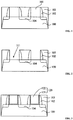
- FIGs 1 ⁇ 9 illustrate intermediate structures corresponding to certain stages of an exemplary fabrication process of a semiconductor device consistent with the disclosed embodiments.
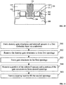
- FIG. 11 illustrates a flow chart of an exemplary fabrication process of a semiconductor device consistent with the disclosed embodiments.
- a substrate 100 is provided, and dummy gate structures 101, a first dielectric layer 103, and sidewall spacers 102 on two sides of each dummy gate structure 101 may be disposed on a surface of the substrate 100.
- the dummy gate structures 101 and the sidewall spacers 102 may be disposed in the first dielectric layer 103, and may level with the top surface of the first electric layer 103.
- Source/drain regions 104 may be formed in the substrate 100 on two sides of the dummy gate structures 101.
- the substrate 100 may be a semiconductor substrate, such as a single-crystalline silicon substrate, a single-crystalline germanium substrate, a silicon germanium substrate, a silicon carbide substrate, a silicon-on-insulator substrate, or a germanium-on-insulator substrate.
- the substrate 100 may also be a semiconductor substrate or fins formed on the semiconductor substrate. In one embodiment, the substrate 100 may be a fin formed on the semiconductor substrate.
- the sidewall spacers 102 may be made of a material selected from silicon nitride, silicon oxynitride, and carbon-doped silicon oxynitride, or any combination thereof. In one embodiment, the sidewall spacers 102 may be made of silicon nitride.
- the first dielectric layer 103 may be used to define the shape and locations of the to-be-formed gate structures, and the material of the first dielectric layer 103 may be silicon oxide, silicon nitride, silicon oxynitride, a low-K dielectric material (the dielectric constant greater than or equal to 2.5, but smaller than 3.9) or an ultra low-K dielectric material (the dielectric constant smaller than 2.5). In one embodiment, the material of the dielectric layer 103 may be silicon oxide.
- the dummy gate structures 101 may be removed, and first openings 111 may be formed between the sidewall spacers 102.
- the method to remove the dummy gate structures 101 may be a dry-etching process.
- the dry-etching process may be an anisotropic dry-etching process or an isotropous dry-etching process.
- the method that removes the dummy gate structures 101 may be a wet-etching process.
- the material of the dummy gate structures 101 may be polycrystalline silicon, and the method to remove the dummy gate structures 101 may be the isotropic dry-etching process.
- a gate structure 120 may be formed in each first opening 111 (as shown in FIG. 2 ), and the top surface of the gate structures 120 may level with the top surface of the first dielectric layer 103.
- Forming the gate structures 120 may include sequentially forming a gate dielectric layer 121 and a gate electrode layer 122 in the first openings 111.
- the gate dielectric layer 121 may have a relatively small thickness and cover a part of the substrate 100 exposed by the first openings 111 and partial surface of the sidewall spacers 102.
- the gate electrode layer 122 may be disposed over the gate dielectric layer 121 and fill each first opening 111.
- the material of the gate dielectric layer 121 may be a high-K dielectric material (the dielectric constant larger than 3.9).
- the high-K dielectric material may include hafnium oxide, zirconium oxide, hafnium zirconium oxide, lanthanum oxide, zirconium silicon oxide, titanium oxide, tantalum oxide, barium strontium titanium oxide, barium titanium oxide, strontium titanium oxide, and aluminium oxide.
- the material of the gate dielectric layer 121 may be hafnium oxide.
- the material of the gate electrode layer 122 may be Cu, W, Al, Au, or Ag. In one embodiment, the material of the gate electrode layer 122 may be W. In some other embodiments, before the gate electrode layer 122 is formed, an insulation layer may be formed over surface of the gate dielectric layer 121, and a work function layer may be formed over surface of the insulation layer. The material of the work function layer may be a metal or a metallic compound.
- each sidewall spacer 102 and a portion of each gate structure 120 may be removed, respectively.
- the top surface of the remaining sidewall spacers 102 and the top surface of the remaining gate structures 120 may be lower than the top surface of the first dielectric layer 103.
- second openings 112 may be formed in the first dielectric layer 103.
- the portion of the sidewall spacers 102 may be removed before or after the portion of the gate structures 120 are removed.
- the portion of the sidewall spacers 102 may be removed first (as shown in FIG. 5 ), and the portion of the gate structures 120 may later be removed (as shown in FIG. 4 ). In some other embodiments, the portion of the gate structures 120 may be removed first, and the portion of the sidewall spacers 102 may later be removed.
- the thickness of the removed portion of the sidewall spacers 102 may be greater than the thickness of the removed portion of the gate structures 120. In some other embodiments, the thickness of the removed portion of the sidewall spacers 102 may be smaller than or equal to the thickness of the removed portion of the gate structures 120. The thickness of the removed portion of the sidewall spacers 102 may range from 100 ⁇ to 1000 ⁇ , and the thickness of the removed portion of the gate structures 120 may range from 100 ⁇ to 1000 ⁇ .
- the thickness of the removed portion of the sidewall spacers 102 may be 200 ⁇ , and the thickness of the removed portion of the gate structures 120 may be 500 ⁇ . That is, the thickness of the removed portion of the sidewall spacers 102 may be smaller than the thickness of the removed portion of the gate structures 120, and the top surface of the remaining sidewall spacers 102 may be above the top surface of the remaining gate structures 120.
- the method to remove the portion of the sidewall spacers 102 may include a dry-etching process, and the dry-etching process may be an etching process with a high selectivity. That is, the rate to etch the sidewall spacers 102 may be higher than the rates to etch the first dielectric layer 103 and the gate structures 120.
- An etching gas for the dry-etching process may be a gas selected from CF 3 I, O 2 , and H 2 , or any combination thereof.
- a flow rate of the etching gas may range from 10 mL/min to 2,000 mL/min, a pressure may range from 3 mtorr to 500 mtorr, and an etching power may range from 100 W to 3,000 W.
- the etching gas used in the dry-etching process may be CF 3 I
- the flow rate of the gas CF 3 I may be 500 mL/min
- the pressure may be 100 mtorr
- the etching power may be 800 W.
- Removing a portion of the gate structures 120 may include removing a portion of the gate dielectric layer 121 and removing a portion of the gate electrode layer 122. In one embodiment.
- the thickness of the removed portion of the gate dielectric layer 121 may be the same as the thickness of the removed portion of the gate electrode layer 122.
- the process to remove a portion of the gate structure 120 may include removing a portion of the gate dielectric layer 121 via a dry or wet etching process, and removing a portion of the gate electrode layer 122 via the dry-etching process.
- a capping layer 131 may be formed to substantially fill the second openings 112 (as illustrated in FIG. 4 ) and level with the top surface of the first dielectric layer 103.
- a method to form the capping layer 131 may include forming the capping layer 131 to fill the second openings 112, and planarizing the capping layer 131, such that the top surface of the capping layer 131 may level with the top surface of the first dielectric layer 103.
- a method to planarize the capping layer 131 may include chemical mechanical polishing, dry-etching, and wet-etching, or any combination thereof. In one embodiment, a plasma etching process may be applied to planarize the capping layer 131. Further, the material of the capping layer 131 may include silicon nitride, titanium nitride, silicon carbide, silicon oxynitride, carbon-doped silicon oxynitride, silicon oxide, and/or aluminium oxide. In one embodiment, the material of the capping layer 131 may be silicon nitride.
- contact structures 151 (e.g., as shown in FIG. 9 ) that are electrically connected to source/drain regions 104 may be formed in the first dielectric layer 103.
- a method to form the contact structures 151 may include a self-alignment contact (SAC) technique.
- SAC self-alignment contact
- FIG. 7 ⁇ FIG. 9 illustrate a method to form the contact structures 151.
- a second dielectric layer 141 may be formed on surface of the first dielectric layer 103 and the capping layer 131.
- a patterned photo-resist layer (not shown) may be disposed on the second dielectric layer 141, and the patterned photo-resist layer may be exposed to provide a region to form the contact structure 151.
- the patterned photo-resist layer may be used as a mask to etch the second dielectric layer 141 and the first dielectric layer 103.
- a third opening 113 may be formed in the second dielectric layer 141 and the first dielectric layer 103.
- the source/drain regions 104 may be exposed at the bottom of the third opening 113.
- the third opening 113 may be filled with an electrically conductive material, and the electrically conductive material may be planarized to form the contact structures 151.
- the electrically conductive material forming the contact structures 151 may include one or more materials selected from W, Al, Ag, Cr, Mo, Ni, Pd, Pt, Ti, Ta and Cu, but the present invention is not limited thereto.
- the electrically conductive material may be Cu, and an electrochemical plating (ECP) method may be applied to fill the third opening 113 with the electrically conductive material.
- ECP electrochemical plating
- any possibly existing gaps between the sidewall spacers 102 and the gate structures 120 maybe covered. Accordingly, the issue regarding a short circuit induced by the electrically conductive material of the contact structures 151 to contact the gate electrode layers 122 via the gaps between the sidewall spacers 102 and the gate electrode layers 122 may be avoided, and performance of semiconductor devices may be improved.
- FIG. 10 illustrates an intermediate structure corresponding to another exemplary fabrication process of a semiconductor device consistent with the disclosed embodiments.
- the thickness of the removed portion of the sidewall spacers 102 may be greater than the thickness of the removed portion of the gate structures 120. That is, the top surface of the sidewall spacers 102 may be lower than the top surface of the gate structures 120.
- the fabrication process to form the sidewall spacers 102, the first dielectric layer 103, the source/drain regions 104, the gate structures 120, the capping layer 131, the second dielectric layer 141, and the contact structures 151 may refer to corresponding descriptions, which are not repeated here.
- the capping layer 131 may still cover possibly existing gaps between the sidewall spacers 102 and the gate structures 120.
- the issue of a short circuit induced by the electrically conductive material of the contact structures 151 to contact the gate electrode layers 122 via the gaps between the sidewall spacers 102 and the gate electrode layers 122 may be avoided, and the performance of the semiconductor devices may be improved.
- FIG. 9 illustrates a cross-sectional view of an exemplary semiconductor device consistent with disclosed embodiments.
- the semiconductor device may include a substrate 100, gate structures 120 disposed on the substrate 100, a first dielectric layer 103, sidewall spacers 102 disposed on two sides of each gate structure 120, a capping layer 131, source/drain regions 104, a second dielectric layer 141, and contact structures 151.
- the gate structures 120 and the sidewall spacers 102 may be disposed in the first dielectric layer 103, and the top surface of the gate structures 120 and the top surface of the sidewall spacers 102 may be lower than the top surface of the first dielectric layer 103.
- the capping layer 131 may be disposed on the gate structures 120 and the sidewall spacers 102, and the top surface of the capping layer 131 may level with the top surface of the first dielectric layer 103.
- the source/drain regions 104 may be located on two sides of each gate structure 120 in the substrate 100.
- the second dielectric layer 141 maybe disposed on the first dielectric layer 103 and the capping layer 131.
- the bottom of the contact structures 151 may get in touch with the source/drain regions 104, and walls of the contact structures 151 may get in touch with the sidewall spacers 102, the capping layer 131, and the second dielectric layer 141, respectively.
- the top surface of the sidewall spacers 102 may be higher than the top surface of the gate structures 120. In some other embodiments, the top surface of the sidewall spacers 102 may be lower than or level with the top surface of the gate structures 120.
- the height of the sidewall spacers 102 may be approximately 50% ⁇ 90% of the height of the first dielectric layer 103.
- the height of the gate structures 120 may be approximately 50% ⁇ 80% of the height of the first dielectric layer 103.
- the top surface of the sidewall spacers 102 may be higher than the top surface of the gate structures 120.
- the height of the sidewall spacers 102 may be approximately 70% of the height of the first dielectric layer 103, and the height of the gate structures 120 may be approximately 50% of the height of the first dielectric layer 103.
- the substrate 100 may be a semiconductor substrate, such as a single-crystalline silicon substrate, a single-crystalline germanium substrate, a silicon germanium substrate, a silicon carbide substrate, a silicon-on-insulator substrate, and/or a germanium-on-insulator substrate.
- the substrate 100 may also be a semiconductor substrate or fins formed on the semiconductor substrate. In one embodiment, the substrate 100 may be a fin formed on the semiconductor substrate.
- the material of the sidewall spacers 102 may include a material selected from silicon nitride, silicon oxynitride, and carbon-doped silicon oxynitride, or any combination thereof. In one embodiment, the material of the sidewall spacers 102 may be silicon nitride.
- Each gate structure 120 may include a gate dielectric layer 121 and a gate electrode layer 122.
- the gate dielectric layer 121 may cover a part of the substrate 100 and side surfaces of the sidewall spacers 102, and the gate electrode layer 122 may be formed over the gate dielectric layer 121.
- the material of the gate dielectric layer 121 may be a high-K dielectric material (the dielectric coefficient greater than 3.9).
- the high-K dielectric material may include hafnium oxide, zirconium oxide, hafnium zirconium oxide, lanthanum oxide, zirconium silicon oxide, titanium oxide, tantalum oxide, barium strontium titanium oxide, barium titanium oxide, strontium titanium oxide, and/or aluminium oxide.
- the material of the gate dielectric layer 121 may be hafnium oxide.
- the material of the gate electrode layer 122 may be Cu, W, Al, Au, and/or Ag. In one embodiment, the material of the gate electrode layer 122 may be W.
- an insulation layer may be formed over the surface of the gate dielectric layer 121, and a work function layer may be formed over the surface of the insulation layer.
- the material of the work function layer may be a metal or a metallic compound.
- the material of the capping layer 131 may include silicon nitride, titanium nitride, silicon carbide, silicon oxynitride, carbon-doped silicon oxynitride, silicon oxide, and/or aluminium oxide. In one embodiment, the material of the capping layer 131 may be silicon nitride.
- the material of the contact structures 151 may be one or more selected from W, Al, Ag, Cr, Mo, Ni, Pd, Pt, Ti, Td and Cu, but the present invention is not limited thereto. In one embodiment, the material of the contact structures 151 maybe Cu.
- FIG. 10 illustrates a cross-sectional view of another exemplary semiconductor device consistent with the disclosed embodiments.
- the height of the sidewall spacers 102 may be smaller than the height of the gate structures 120.
- the height of the sidewall spacers 102 may be 50% of the height of the first dielectric layer 103, and the height of the gate structures 120 may be 70% of the height of the first dielectric layer 103.
- the structures of the gate structures 120, the first dielectric layer 103, the sidewall spacers 102, the capping layer 131, the source/drain regions 104, the second dielectric layer 141 and the contact structures 151 may refer to corresponding descriptions, which are not repeated here.
- the fabrication method of the disclosed semiconductor device may include removing a portion of the sidewall spacers and a portion of the gate structures, respectively, after removing the dummy gate structures and forming the gate structures. Further, the fabrication method may include forming a capping layer on the sidewall spacers and the gate structures. Accordingly, the fabricated contact structures may be electrically connected to the source/drain regions and, simultaneously be isolated from the gate structures by the capping layer on the sidewall spacers. Thus, the short circuit issue induced by the electrically conductive material of the contact structure to contact the gate structure may be effectively avoided, and the performance of the semiconductor devices may be improved.
- a portion of the sidewall spacers and a portion of the gate structures may be removed after the dummy gate structures are removed and the gate structures are formed. Accordingly, the fabrication of the semiconductor device may be simplified and the whole process may be completed in a gate electrode etching machine.
- the contact structures may be electrically connected to the source/drain regions and, simultaneously be isolated from the gate structures by the capping layer.
- the issue that the contact structure will contact the gate structure to induce a short circuit may be effectively avoided, and the performance of the semiconductor device may be improved.
Landscapes
- Insulated Gate Type Field-Effect Transistor (AREA)
- Internal Circuitry In Semiconductor Integrated Circuit Devices (AREA)
- Electrodes Of Semiconductors (AREA)
Abstract
Description
- This application claims the priority of Chinese patent application No.
201610216931.4, filed on April 8,2016 - The present invention generally relates to the field of semiconductor manufacturing technology and, more particularly, relates to a semiconductor device and fabrication method thereof.
- In semiconductor devices, multilayer circuits may be formed on a silicon wafer and may often be electrically connected via a contact structure. When fabricating the contact structure, first, an interlayer dielectric (ILD) layer is etched to form trenches or through-holes (also named openings). Then, an electrically conductive material is used to fill the trenches or through-holes to form the contact structure. With the rapid development of very-large-scale integration (VLSI) circuits, critical dimensions of circuit components continuously decrease, thus demanding higher requirements of the photolithographic process.
- In semiconductor manufacturing processes, a self-alignment contact (SAC) technique is often applied to form contact structures. The SAC technique attracts wide attention because it lowers the requirement of photolithographic precision, and further reduces the area needed to form transistors.
- However, when utilizing the SAC technique to form a contact structure on a source electrode or a drain electrode, the contact structure may easily touch a gate electrode, thus forming a short circuit that influences the performance of the semiconductor device. Accordingly, it is desirable to avoid the short circuit formed between the contact structure and the gate electrode in semiconductor devices.
- It is an object of the present invention to provide a semiconductor device and fabrication method which at least partially solve one or more problems set forth above and other problems.
- The object is achieved by the features of the respective independent claims. Further embodiments are defined in the respective dependent claims.
- A first aspect of the present invention provides a method for fabricating a semiconductor device. The method includes forming at least one dummy gate structure and sidewall spacers of the dummy gate structure in a first dielectric layer, together on a substrate and removing the dummy gate structure, thereby forming a first opening between the sidewall spacers. The method further includes forming a gate structure in the first opening and having a top surface levelled with a top surface of the first dielectric layer, removing a portion of the sidewall spacers and a portion of the gate structure, respectively, to form a second opening in the first dielectric layer, on remaining sidewall spacers, and on remaining gate structure, and forming a capping layer to fill the second opening and to have a top surface levelled with the top surface of the first dielectric layer.
- Preferably, the dummy gate structure, the sidewall spacers, and the first dielectric layer have a coplanar top surface.
- Preferably, a thickness of a removed portion of the sidewall spacers is greater than a thickness of a removed portion of the gate structure.
- Preferably, a thickness of a removed portion of the sidewall spacers is less than or equal to a thickness of a removed portion of the gate structure.
- Preferably, a thickness of a removed portion of the sidewall spacers ranges from 100 Å to 1000 Å.
- Preferably, a thickness of a removed portion of the gate structure ranges from 100 Å to 1000 Å.
- Preferably, the portion of the sidewall spacers is removed before or after the portion of the gate structure is removed.
- Preferably, removing the portion of the sidewall spacers includes a dry etching process. Preferably, an etching gas for the dry etching process includes one or more gases selected from CF3I, O2, and H2.
- Preferably, forming the gate structure in the first opening comprises: forming a gate dielectric layer on a surface of the substrate and on the sidewall spacers of the first opening; and forming a gate electrode layer over the gate dielectric layer to fill the first opening.
- Preferably, removing the portion of the gate structure comprises: using a dry or wet etching process to remove a portion of the gate dielectric layer; and using the dry etching process to remove a portion of the gate electrode layer.
- Preferably, the capping layer is made of one or more materials selected from silicon nitride, titanium nitride, silicon carbide, silicon oxynitride, and carbon-doped silicon oxynitride.
- Preferably, the sidewall spacers is made of one or more materials selected from silicon nitride, silicon oxynitride, and carbon-doped silicon oxynitride.
- Preferably, the method further comprises: forming source/drain regions on sides of the dummy gate electrode in the substrate; and after forming the capping layer, forming contact structures in the first dielectric layer to electrically connect to the source/drain regions.
- Preferably, the contact structures are formed by: forming a second dielectric layer on the first dielectric layer and the capping layer; forming a third opening in the second dielectric layer and the first dielectric layer to expose the source/drain regions; filling the third opening with an electrically conductive material; and planarizing the electrically conductive material to form the contact structures.
- A second aspect of the present invention provides a semiconductor device. The semiconductor device includes a substrate, a plurality of gate structures and sidewall spacers of each gate structure, a first dielectric layer, a capping layer, source/drain regions, a second dielectric layer and contact structures. The plurality of gate structures and sidewall spacers of each gate structure are disposed in the first dielectric layer, together on the substrate. The capping layer is disposed on each gate structure and the sidewall spacers, and has a top surface levelled with a top surface of the first dielectric layer. The source/drain regions are on sides of the gate structures in the substrate. The second dielectric layer is disposed on the first dielectric layer and the capping layer. The contact structures are formed on the source/drain regions and each has a surface in contact with adjacent sidewall spacers, the capping layer, and the second dielectric layer.
- Preferably, a top surface of the sidewall spacers are higher than a top surface of the plurality of gate structures.
- Preferably, a top surface of the sidewall spacers are lower than or level with a top surface of the plurality of gate structures.
- Preferably, a height of the sidewall spacers is approximately 50%∼90% of a height of the first dielectric layer.
- Preferably, a height of the plurality of gate structures is approximately 50%∼80% of the height of the first dielectric layer.
- Preferably, the capping layer is made of one or more materials selected from silicon nitride, titanium nitride, silicon carbide, silicon oxynitride, and carbon-doped silicon oxynitride.
- Preferably, the sidewall spacers is made of one or more materials selected from silicon nitride, silicon oxynitride, and carbon-doped silicon oxynitride.
- A semiconductor device according to the second aspect of the present invention is obtainable by a method for fabricating a semiconductor device according to the first aspect of the present invention.
- Other aspects of the present invention can be understood by those skilled in the art in light of the description, the claims, and the drawings of the present invention.
-
-
FIGs 1∼9 illustrate intermediate structures corresponding to certain stages of an exemplary fabrication process of a semiconductor device consistent with the disclosed embodiments; -
FIG. 10 illustrates an intermediate structure corresponding to certain stages of another exemplary fabrication process of a semiconductor device consistent with the disclosed embodiments; and -
FIG. 11 illustrates a flow chart of an exemplary fabrication process of a semiconductor device consistent with the disclosed embodiments. - Reference will now be made in detail to exemplary embodiments of the disclosure, which are illustrated in the accompanying drawings. Wherever possible, the same reference numbers will be used throughout the drawings to refer to the same or like parts.
- The present invention provides a semiconductor device and fabrication method thereof. The disclosed device and method may effectively solve the short circuit issues and thus to improve performance of the fabricated semiconductor device. According to the present invention, a gate structure is formed in the first opening between the sidewall spacers, and a portion of the sidewall spacers and a portion of the gate structures are removed after the gate structure is formed. Thus, the fabrication of the semiconductor device may be simplified and the whole process may be completed in a gate electrode etching machine.
-
FIGs 1∼9 illustrate intermediate structures corresponding to certain stages of an exemplary fabrication process of a semiconductor device consistent with the disclosed embodiments.FIG. 11 illustrates a flow chart of an exemplary fabrication process of a semiconductor device consistent with the disclosed embodiments. - In step 1 (S01) of
FIG. 11 and referring toFIG. 1 , asubstrate 100 is provided, anddummy gate structures 101, a firstdielectric layer 103, andsidewall spacers 102 on two sides of eachdummy gate structure 101 may be disposed on a surface of thesubstrate 100. For example, thedummy gate structures 101 and thesidewall spacers 102 may be disposed in the firstdielectric layer 103, and may level with the top surface of the firstelectric layer 103. Source/drain regions 104 may be formed in thesubstrate 100 on two sides of thedummy gate structures 101. - The
substrate 100 may be a semiconductor substrate, such as a single-crystalline silicon substrate, a single-crystalline germanium substrate, a silicon germanium substrate, a silicon carbide substrate, a silicon-on-insulator substrate, or a germanium-on-insulator substrate. Thesubstrate 100 may also be a semiconductor substrate or fins formed on the semiconductor substrate. In one embodiment, thesubstrate 100 may be a fin formed on the semiconductor substrate. - The sidewall spacers 102 may be made of a material selected from silicon nitride, silicon oxynitride, and carbon-doped silicon oxynitride, or any combination thereof. In one embodiment, the
sidewall spacers 102 may be made of silicon nitride. - The
first dielectric layer 103 may be used to define the shape and locations of the to-be-formed gate structures, and the material of thefirst dielectric layer 103 may be silicon oxide, silicon nitride, silicon oxynitride, a low-K dielectric material (the dielectric constant greater than or equal to 2.5, but smaller than 3.9) or an ultra low-K dielectric material (the dielectric constant smaller than 2.5). In one embodiment, the material of thedielectric layer 103 may be silicon oxide. - In step 2 (S02) of
FIG. 11 and referring toFIG. 2 , thedummy gate structures 101 may be removed, andfirst openings 111 may be formed between thesidewall spacers 102. The method to remove thedummy gate structures 101 may be a dry-etching process. The dry-etching process may be an anisotropic dry-etching process or an isotropous dry-etching process. Optionally, the method that removes thedummy gate structures 101 may be a wet-etching process. In one embodiment, the material of thedummy gate structures 101 may be polycrystalline silicon, and the method to remove thedummy gate structures 101 may be the isotropic dry-etching process. - In step 3 (S03) of
FIG. 11 and referring toFIG. 3 , agate structure 120 may be formed in each first opening 111 (as shown inFIG. 2 ), and the top surface of thegate structures 120 may level with the top surface of thefirst dielectric layer 103. Forming thegate structures 120 may include sequentially forming agate dielectric layer 121 and agate electrode layer 122 in thefirst openings 111. In one embodiment, thegate dielectric layer 121 may have a relatively small thickness and cover a part of thesubstrate 100 exposed by thefirst openings 111 and partial surface of thesidewall spacers 102. Thegate electrode layer 122 may be disposed over thegate dielectric layer 121 and fill eachfirst opening 111. - The material of the
gate dielectric layer 121 may be a high-K dielectric material (the dielectric constant larger than 3.9). The high-K dielectric material may include hafnium oxide, zirconium oxide, hafnium zirconium oxide, lanthanum oxide, zirconium silicon oxide, titanium oxide, tantalum oxide, barium strontium titanium oxide, barium titanium oxide, strontium titanium oxide, and aluminium oxide. In one embodiment, the material of thegate dielectric layer 121 may be hafnium oxide. - The material of the
gate electrode layer 122 may be Cu, W, Al, Au, or Ag. In one embodiment, the material of thegate electrode layer 122 may be W. In some other embodiments, before thegate electrode layer 122 is formed, an insulation layer may be formed over surface of thegate dielectric layer 121, and a work function layer may be formed over surface of the insulation layer. The material of the work function layer may be a metal or a metallic compound. - In step 4 (S04) of
FIG. 11 and referring toFIG. 4 , a portion of eachsidewall spacer 102 and a portion of eachgate structure 120 may be removed, respectively. Thus, the top surface of the remainingsidewall spacers 102 and the top surface of the remaininggate structures 120 may be lower than the top surface of thefirst dielectric layer 103. Accordingly,second openings 112 may be formed in thefirst dielectric layer 103. The portion of thesidewall spacers 102 may be removed before or after the portion of thegate structures 120 are removed. - In one embodiment, the portion of the
sidewall spacers 102 may be removed first (as shown inFIG. 5 ), and the portion of thegate structures 120 may later be removed (as shown inFIG. 4 ). In some other embodiments, the portion of thegate structures 120 may be removed first, and the portion of thesidewall spacers 102 may later be removed. - In some embodiments, the thickness of the removed portion of the
sidewall spacers 102 may be greater than the thickness of the removed portion of thegate structures 120. In some other embodiments, the thickness of the removed portion of thesidewall spacers 102 may be smaller than or equal to the thickness of the removed portion of thegate structures 120. The thickness of the removed portion of thesidewall spacers 102 may range from 100 Å to 1000 Å, and the thickness of the removed portion of thegate structures 120 may range from 100 Å to 1000 Å. - In one embodiment, the thickness of the removed portion of the
sidewall spacers 102 may be 200 Å, and the thickness of the removed portion of thegate structures 120 may be 500 Å. That is, the thickness of the removed portion of thesidewall spacers 102 may be smaller than the thickness of the removed portion of thegate structures 120, and the top surface of the remainingsidewall spacers 102 may be above the top surface of the remaininggate structures 120. - The method to remove the portion of the
sidewall spacers 102 may include a dry-etching process, and the dry-etching process may be an etching process with a high selectivity. That is, the rate to etch thesidewall spacers 102 may be higher than the rates to etch thefirst dielectric layer 103 and thegate structures 120. An etching gas for the dry-etching process may be a gas selected from CF3I, O2, and H2, or any combination thereof. A flow rate of the etching gas may range from 10 mL/min to 2,000 mL/min, a pressure may range from 3 mtorr to 500 mtorr, and an etching power may range from 100 W to 3,000 W. In one embodiment, the etching gas used in the dry-etching process may be CF3I, the flow rate of the gas CF3I may be 500 mL/min, the pressure may be 100 mtorr, and the etching power may be 800 W. - Removing a portion of the
gate structures 120 may include removing a portion of thegate dielectric layer 121 and removing a portion of thegate electrode layer 122. In one embodiment. The thickness of the removed portion of thegate dielectric layer 121 may be the same as the thickness of the removed portion of thegate electrode layer 122. The process to remove a portion of thegate structure 120 may include removing a portion of thegate dielectric layer 121 via a dry or wet etching process, and removing a portion of thegate electrode layer 122 via the dry-etching process. - In step 5 (S05) of
FIG. 11 and referring toFIG. 6 , acapping layer 131 may be formed to substantially fill the second openings 112 (as illustrated inFIG. 4 ) and level with the top surface of thefirst dielectric layer 103. A method to form thecapping layer 131 may include forming thecapping layer 131 to fill thesecond openings 112, and planarizing thecapping layer 131, such that the top surface of thecapping layer 131 may level with the top surface of thefirst dielectric layer 103. - A method to planarize the
capping layer 131 may include chemical mechanical polishing, dry-etching, and wet-etching, or any combination thereof. In one embodiment, a plasma etching process may be applied to planarize thecapping layer 131. Further, the material of thecapping layer 131 may include silicon nitride, titanium nitride, silicon carbide, silicon oxynitride, carbon-doped silicon oxynitride, silicon oxide, and/or aluminium oxide. In one embodiment, the material of thecapping layer 131 may be silicon nitride. - After forming the
capping layer 131, contact structures 151 (e.g., as shown inFIG. 9 ) that are electrically connected to source/drain regions 104 may be formed in thefirst dielectric layer 103. In one embodiment, a method to form thecontact structures 151 may include a self-alignment contact (SAC) technique. -
FIG. 7∼FIG. 9 illustrate a method to form thecontact structures 151. Referring toFIG.7 , asecond dielectric layer 141 may be formed on surface of thefirst dielectric layer 103 and thecapping layer 131. A patterned photo-resist layer (not shown) may be disposed on thesecond dielectric layer 141, and the patterned photo-resist layer may be exposed to provide a region to form thecontact structure 151. Referring toFIG. 8 , the patterned photo-resist layer may be used as a mask to etch thesecond dielectric layer 141 and thefirst dielectric layer 103. Athird opening 113 may be formed in thesecond dielectric layer 141 and thefirst dielectric layer 103. The source/drain regions 104 may be exposed at the bottom of thethird opening 113. - Referring to
FIG. 9 , thethird opening 113 may be filled with an electrically conductive material, and the electrically conductive material may be planarized to form thecontact structures 151. The electrically conductive material forming thecontact structures 151 may include one or more materials selected from W, Al, Ag, Cr, Mo, Ni, Pd, Pt, Ti, Ta and Cu, but the present invention is not limited thereto. For example, in the present invention, the electrically conductive material may be Cu, and an electrochemical plating (ECP) method may be applied to fill thethird opening 113 with the electrically conductive material. - Because the
contact structures 151 and thegate structures 120 are isolated by thecapping layer 131 and thesidewall spacer 102 and thecapping layer 131 is disposed over thesidewall spacers 102 and extends transversely, any possibly existing gaps between thesidewall spacers 102 and thegate structures 120 maybe covered. Accordingly, the issue regarding a short circuit induced by the electrically conductive material of thecontact structures 151 to contact the gate electrode layers 122 via the gaps between thesidewall spacers 102 and the gate electrode layers 122 may be avoided, and performance of semiconductor devices may be improved. -
FIG. 10 illustrates an intermediate structure corresponding to another exemplary fabrication process of a semiconductor device consistent with the disclosed embodiments. Referring toFIG. 10 , different from the above-described fabrication process, in one embodiment, the thickness of the removed portion of thesidewall spacers 102 may be greater than the thickness of the removed portion of thegate structures 120. That is, the top surface of thesidewall spacers 102 may be lower than the top surface of thegate structures 120. - In one embodiment, the fabrication process to form the
sidewall spacers 102, thefirst dielectric layer 103, the source/drain regions 104, thegate structures 120, thecapping layer 131, thesecond dielectric layer 141, and thecontact structures 151 may refer to corresponding descriptions, which are not repeated here. - In one embodiment, the
capping layer 131 may still cover possibly existing gaps between thesidewall spacers 102 and thegate structures 120. Thus, the issue of a short circuit induced by the electrically conductive material of thecontact structures 151 to contact the gate electrode layers 122 via the gaps between thesidewall spacers 102 and the gate electrode layers 122 may be avoided, and the performance of the semiconductor devices may be improved. - Correspondingly, the present invention also provides a semiconductor device. Referring to
FIG. 9, FIG. 9 illustrates a cross-sectional view of an exemplary semiconductor device consistent with disclosed embodiments. The semiconductor device may include asubstrate 100,gate structures 120 disposed on thesubstrate 100, a firstdielectric layer 103,sidewall spacers 102 disposed on two sides of eachgate structure 120, acapping layer 131, source/drain regions 104, asecond dielectric layer 141, andcontact structures 151. - The
gate structures 120 and thesidewall spacers 102 may be disposed in thefirst dielectric layer 103, and the top surface of thegate structures 120 and the top surface of thesidewall spacers 102 may be lower than the top surface of thefirst dielectric layer 103. Thecapping layer 131 may be disposed on thegate structures 120 and thesidewall spacers 102, and the top surface of thecapping layer 131 may level with the top surface of thefirst dielectric layer 103. The source/drain regions 104 may be located on two sides of eachgate structure 120 in thesubstrate 100. Thesecond dielectric layer 141 maybe disposed on thefirst dielectric layer 103 and thecapping layer 131. The bottom of thecontact structures 151 may get in touch with the source/drain regions 104, and walls of thecontact structures 151 may get in touch with thesidewall spacers 102, thecapping layer 131, and thesecond dielectric layer 141, respectively. - In some embodiments, the top surface of the
sidewall spacers 102 may be higher than the top surface of thegate structures 120. In some other embodiments, the top surface of thesidewall spacers 102 may be lower than or level with the top surface of thegate structures 120. The height of thesidewall spacers 102 may be approximately 50%∼90% of the height of thefirst dielectric layer 103. The height of thegate structures 120 may be approximately 50%∼80% of the height of thefirst dielectric layer 103. - In one embodiment, the top surface of the
sidewall spacers 102 may be higher than the top surface of thegate structures 120. The height of thesidewall spacers 102 may be approximately 70% of the height of thefirst dielectric layer 103, and the height of thegate structures 120 may be approximately 50% of the height of thefirst dielectric layer 103. - The
substrate 100 may be a semiconductor substrate, such as a single-crystalline silicon substrate, a single-crystalline germanium substrate, a silicon germanium substrate, a silicon carbide substrate, a silicon-on-insulator substrate, and/or a germanium-on-insulator substrate. Thesubstrate 100 may also be a semiconductor substrate or fins formed on the semiconductor substrate. In one embodiment, thesubstrate 100 may be a fin formed on the semiconductor substrate. - The material of the
sidewall spacers 102 may include a material selected from silicon nitride, silicon oxynitride, and carbon-doped silicon oxynitride, or any combination thereof. In one embodiment, the material of thesidewall spacers 102 may be silicon nitride. - Each
gate structure 120 may include agate dielectric layer 121 and agate electrode layer 122. In particular, thegate dielectric layer 121 may cover a part of thesubstrate 100 and side surfaces of thesidewall spacers 102, and thegate electrode layer 122 may be formed over thegate dielectric layer 121. - The material of the
gate dielectric layer 121 may be a high-K dielectric material (the dielectric coefficient greater than 3.9). The high-K dielectric material may include hafnium oxide, zirconium oxide, hafnium zirconium oxide, lanthanum oxide, zirconium silicon oxide, titanium oxide, tantalum oxide, barium strontium titanium oxide, barium titanium oxide, strontium titanium oxide, and/or aluminium oxide. In one embodiment, the material of thegate dielectric layer 121 may be hafnium oxide. - The material of the
gate electrode layer 122 may be Cu, W, Al, Au, and/or Ag. In one embodiment, the material of thegate electrode layer 122 may be W. Before forming thegate electrode layer 122, an insulation layer may be formed over the surface of thegate dielectric layer 121, and a work function layer may be formed over the surface of the insulation layer. The material of the work function layer may be a metal or a metallic compound. - The material of the
capping layer 131 may include silicon nitride, titanium nitride, silicon carbide, silicon oxynitride, carbon-doped silicon oxynitride, silicon oxide, and/or aluminium oxide. In one embodiment, the material of thecapping layer 131 may be silicon nitride. - The material of the
contact structures 151 may be one or more selected from W, Al, Ag, Cr, Mo, Ni, Pd, Pt, Ti, Td and Cu, but the present invention is not limited thereto. In one embodiment, the material of thecontact structures 151 maybe Cu. - Referring to
FIG. 10, FIG. 10 illustrates a cross-sectional view of another exemplary semiconductor device consistent with the disclosed embodiments. Different from the above-described semiconductor device, in one embodiment, as shown inFIG. 10 , the height of thesidewall spacers 102 may be smaller than the height of thegate structures 120. In one embodiment, the height of thesidewall spacers 102 may be 50% of the height of thefirst dielectric layer 103, and the height of thegate structures 120 may be 70% of the height of thefirst dielectric layer 103. - The structures of the
gate structures 120, thefirst dielectric layer 103, thesidewall spacers 102, thecapping layer 131, the source/drain regions 104, thesecond dielectric layer 141 and thecontact structures 151 may refer to corresponding descriptions, which are not repeated here. - Accordingly, the fabrication method of the disclosed semiconductor device may include removing a portion of the sidewall spacers and a portion of the gate structures, respectively, after removing the dummy gate structures and forming the gate structures. Further, the fabrication method may include forming a capping layer on the sidewall spacers and the gate structures. Accordingly, the fabricated contact structures may be electrically connected to the source/drain regions and, simultaneously be isolated from the gate structures by the capping layer on the sidewall spacers. Thus, the short circuit issue induced by the electrically conductive material of the contact structure to contact the gate structure may be effectively avoided, and the performance of the semiconductor devices may be improved.
- Further, instead of etching and removing a portion of the sidewall spacers before removing the dummy gate structures, according to the disclosed fabrication process, a portion of the sidewall spacers and a portion of the gate structures may be removed after the dummy gate structures are removed and the gate structures are formed. Accordingly, the fabrication of the semiconductor device may be simplified and the whole process may be completed in a gate electrode etching machine.
- In the disclosed semiconductor device, because the capping layer is disposed on the sidewall spacers and the gate structures, the contact structures may be electrically connected to the source/drain regions and, simultaneously be isolated from the gate structures by the capping layer. Thus, the issue that the contact structure will contact the gate structure to induce a short circuit may be effectively avoided, and the performance of the semiconductor device may be improved.
Claims (15)
- A method for fabricating a semiconductor device, comprising:forming at least one dummy gate structure and sidewall spacers of the dummy gate structure in a first dielectric layer, together on a substrate;removing the dummy gate structure, thereby forming a first opening between the sidewall spacers;forming a gate structure in the first opening and having a top surface levelled with the first dielectric layer;removing a portion of the sidewall spacers and a portion of the gate structure, respectively, to form a second opening in the first dielectric layer, on remaining sidewall spacers, and on remaining gate structure; andforming a capping layer to fill the second opening and to have a top surface levelled with the first dielectric layer.
- The method according to claim 1, wherein:the dummy gate structure, the sidewall spacers, and the first dielectric layer have a coplanar top surface.
- The method according to claim 1 or 2, wherein:a thickness of the removed portion of the sidewall spacers is greater than a thickness of the removed portion of the gate structure; or, alternatively, a thickness of the removed portion of the sidewall spacers is less than or equal to a thickness of the removed portion of the gate structure.
- The method according to any one of the claims 1-3, wherein:a thickness of a removed portion of the sidewall spacers ranges from 100 Å to 1000 Å; and/or a thickness of a removed portion of the gate structure ranges from 100 Å to 1000 Å.
- The method according to any one of the claims 1-4, wherein:the portion of the sidewall spacers is removed before or after the portion of the gate structure is removed.
- The method according to any one of the claims 1-5, wherein:removing the portion of the sidewall spacers includes a dry etching process, andan etching gas for the dry etching process includes one or more gases selected from CF3I, O2, and H2.
- The method according to any one of the claims 1-6, wherein forming the gate structure in the first opening comprises:forming a gate dielectric layer on a surface of the substrate and on the sidewall spacers of the first opening; andforming a gate electrode layer over the gate dielectric layer to fill the first opening;wherein preferably removing the portion of the gate structure comprises: using a dry or wet etching process to remove a portion of the gate dielectric layer; and using the dry etching process to remove a portion of the gate electrode layer.
- The method according to any one of the claims 1-7, wherein:the capping layer is made of one or more materials selected from silicon nitride, titanium nitride, silicon carbide, silicon oxynitride, and carbon-doped silicon oxynitride.
- The method according to any one of the claims 1-8, wherein:the sidewall spacers is made of one or more materials selected from silicon nitride, silicon oxynitride, and carbon-doped silicon oxynitride.
- The method according to any one of the claims 1-9, further comprising:forming source/drain regions on sides of the dummy gate electrode in the substrate; andafter forming the capping layer, forming contact structures in the first dielectric layer to electrically connect to the source/drain regions;wherein preferably the contact structures are formed by: forming a second dielectric layer on the first dielectric layer and the capping layer; forming a third opening in the second dielectric layer and the first dielectric layer to expose the source/drain regions; filling the third opening with an electrically conductive material; and planarizing the electrically conductive material to form the contact structures.
- A semiconductor device, comprising:a substrate;a plurality of gate structures and sidewall spacers of each gate structure disposed in a first dielectric layer, together on the substrate;a capping layer, disposed on each gate structure and the sidewall spacers and having a top surface levelled with the first dielectric layer;source/drain regions on sides of the gate structures in the substrate;a second dielectric layer disposed on the first dielectric layer and the capping layer; andcontact structures formed on the source/drain regions and each having a surface in contact with adjacent sidewall spacers, the capping layer, and the second dielectric layer.
- The semiconductor device according to claim 11, wherein
a top surface of the sidewall spacers are higher than a top surface of the plurality of gate structures; or, alternatively,
a top surface of the sidewall spacers are lower than or level with a top surface of the plurality of gate structures. - The semiconductor device according to claim 11 or 12, wherein:a height of the sidewall spacers is approximately 50%∼90% of a height of the first dielectric layer; anda height of the plurality of gate structures is approximately 50%∼80% of the height of the first dielectric layer.
- The semiconductor device according to any one of the claims 11-13, wherein:the capping layer is made of one or more materials selected from silicon nitride, titanium nitride, silicon carbide, silicon oxynitride, and carbon-doped silicon oxynitride.
- The semiconductor device according to any one of the claims 11-14, wherein:the sidewall spacers is made of one or more materials selected from silicon nitride, silicon oxynitride, and carbon-doped silicon oxynitride.
Applications Claiming Priority (1)
| Application Number | Priority Date | Filing Date | Title |
|---|---|---|---|
| CN201610216931.4A CN107275214A (en) | 2016-04-08 | 2016-04-08 | Semiconductor devices and forming method thereof |
Publications (1)
| Publication Number | Publication Date |
|---|---|
| EP3229263A1 true EP3229263A1 (en) | 2017-10-11 |
Family
ID=58464300
Family Applications (1)
| Application Number | Title | Priority Date | Filing Date |
|---|---|---|---|
| EP17163841.4A Withdrawn EP3229263A1 (en) | 2016-04-08 | 2017-03-30 | Semiconductor device and fabrication method thereof |
Country Status (3)
| Country | Link |
|---|---|
| US (1) | US20170294535A1 (en) |
| EP (1) | EP3229263A1 (en) |
| CN (1) | CN107275214A (en) |
Families Citing this family (5)
| Publication number | Priority date | Publication date | Assignee | Title |
|---|---|---|---|---|
| US10510851B2 (en) * | 2016-11-29 | 2019-12-17 | Taiwan Semiconductor Manufacturing Company, Ltd. | Low resistance contact method and structure |
| CN113327980B (en) * | 2020-02-28 | 2023-03-28 | 中芯国际集成电路制造(天津)有限公司 | Semiconductor structure and forming method thereof |
| US11232947B1 (en) | 2020-09-01 | 2022-01-25 | Taiwan Semiconductor Manufacturing Company Limited | Ammonium fluoride pre-clean protection |
| KR102877107B1 (en) * | 2021-03-12 | 2025-10-28 | 삼성전자주식회사 | Semiconductor device |
| CN113437066B (en) * | 2021-06-23 | 2024-04-12 | 福建省晋华集成电路有限公司 | Semiconductor structure and manufacturing method thereof |
Citations (8)
| Publication number | Priority date | Publication date | Assignee | Title |
|---|---|---|---|---|
| EP0854502A2 (en) * | 1997-01-21 | 1998-07-22 | Texas Instruments Incorporated | Iodofluorocarbon gas for the etching of dielectric layers and the cleaning of process chambers |
| US20110156107A1 (en) * | 2009-12-30 | 2011-06-30 | Bohr Mark T | Self-aligned contacts |
| US20130181265A1 (en) * | 2012-01-18 | 2013-07-18 | Globalfoundries Inc. | Methods of Forming a Gate Cap Layer Above a Replacement Gate Structure and a Semiconductor Device That Includes Such a Gate Structure and Cap Layer |
| US20130187203A1 (en) * | 2012-01-19 | 2013-07-25 | International Business Machines Corporation | Formation of the dielectric cap layer for a replacement gate structure |
| US20140231885A1 (en) * | 2013-02-21 | 2014-08-21 | International Business Machines Corporation | Integrated circuits and methods for fabricating integrated circuits having metal gate electrodes |
| US20150187945A1 (en) * | 2014-01-02 | 2015-07-02 | Globalfoundries Inc. | Salicide protection during contact metallization and resulting semiconductor structures |
| US20150348845A1 (en) * | 2014-05-30 | 2015-12-03 | Taiwan Semiconductor Manufacturing Company, Ltd. | Method of manufacturing a semiconductor device |
| US20160056262A1 (en) * | 2014-08-20 | 2016-02-25 | Taiwan Semiconductor Manufacturing Company Ltd. | Metal gate and manufuacturing process thereof |
Family Cites Families (11)
| Publication number | Priority date | Publication date | Assignee | Title |
|---|---|---|---|---|
| US8421077B2 (en) * | 2010-06-08 | 2013-04-16 | International Business Machines Corporation | Replacement gate MOSFET with self-aligned diffusion contact |
| US8928048B2 (en) * | 2013-01-17 | 2015-01-06 | Globalfoundries Inc. | Methods of forming semiconductor device with self-aligned contact elements and the resulting device |
| US9257348B2 (en) * | 2013-08-06 | 2016-02-09 | Globalfoundries Inc. | Methods of forming replacement gate structures for transistors and the resulting devices |
| US9236480B2 (en) * | 2013-10-02 | 2016-01-12 | Globalfoundries Inc. | Methods of forming finFET semiconductor devices using a replacement gate technique and the resulting devices |
| US9412656B2 (en) * | 2014-02-14 | 2016-08-09 | Taiwan Semiconductor Manufacturing Co., Ltd. | Reverse tone self-aligned contact |
| KR102191219B1 (en) * | 2014-05-14 | 2020-12-16 | 삼성전자주식회사 | Semiconductor device and method for manufacturing the same |
| US9634115B2 (en) * | 2014-06-11 | 2017-04-25 | Globalfoundries Inc. | Methods of forming a protection layer on a semiconductor device and the resulting device |
| KR102276642B1 (en) * | 2014-07-28 | 2021-07-15 | 삼성전자주식회사 | Semiconductor device and method for manufacturing the same |
| US9425103B2 (en) * | 2014-12-04 | 2016-08-23 | Globalfoundries Inc. | Methods of using a metal protection layer to form replacement gate structures for semiconductor devices |
| US9824920B2 (en) * | 2016-04-04 | 2017-11-21 | Globalfoundries Inc. | Methods of forming self-aligned contact structures by work function material layer recessing and the resulting devices |
| US9666533B1 (en) * | 2016-06-30 | 2017-05-30 | International Business Machines Corporation | Airgap formation between source/drain contacts and gates |
-
2016
- 2016-04-08 CN CN201610216931.4A patent/CN107275214A/en active Pending
-
2017
- 2017-02-20 US US15/436,897 patent/US20170294535A1/en not_active Abandoned
- 2017-03-30 EP EP17163841.4A patent/EP3229263A1/en not_active Withdrawn
Patent Citations (8)
| Publication number | Priority date | Publication date | Assignee | Title |
|---|---|---|---|---|
| EP0854502A2 (en) * | 1997-01-21 | 1998-07-22 | Texas Instruments Incorporated | Iodofluorocarbon gas for the etching of dielectric layers and the cleaning of process chambers |
| US20110156107A1 (en) * | 2009-12-30 | 2011-06-30 | Bohr Mark T | Self-aligned contacts |
| US20130181265A1 (en) * | 2012-01-18 | 2013-07-18 | Globalfoundries Inc. | Methods of Forming a Gate Cap Layer Above a Replacement Gate Structure and a Semiconductor Device That Includes Such a Gate Structure and Cap Layer |
| US20130187203A1 (en) * | 2012-01-19 | 2013-07-25 | International Business Machines Corporation | Formation of the dielectric cap layer for a replacement gate structure |
| US20140231885A1 (en) * | 2013-02-21 | 2014-08-21 | International Business Machines Corporation | Integrated circuits and methods for fabricating integrated circuits having metal gate electrodes |
| US20150187945A1 (en) * | 2014-01-02 | 2015-07-02 | Globalfoundries Inc. | Salicide protection during contact metallization and resulting semiconductor structures |
| US20150348845A1 (en) * | 2014-05-30 | 2015-12-03 | Taiwan Semiconductor Manufacturing Company, Ltd. | Method of manufacturing a semiconductor device |
| US20160056262A1 (en) * | 2014-08-20 | 2016-02-25 | Taiwan Semiconductor Manufacturing Company Ltd. | Metal gate and manufuacturing process thereof |
Also Published As
| Publication number | Publication date |
|---|---|
| US20170294535A1 (en) | 2017-10-12 |
| CN107275214A (en) | 2017-10-20 |
Similar Documents
| Publication | Publication Date | Title |
|---|---|---|
| US10658485B2 (en) | Semiconductor device and manufacturing method thereof | |
| CN107546203B (en) | Semiconductor device and method for manufacturing the same | |
| CN104009003B (en) | Integrated circuits and methods for fabricating integrated circuits having metal gate electrodes | |
| CN112151615B (en) | Semiconductor device and method of manufacturing the same | |
| CN107170825B (en) | Semiconductor device, fin field effect transistor device and method of forming the same | |
| CN111128887B (en) | Method of forming semiconductor device | |
| TW201717398A (en) | Semiconductor device and method of manufacturing same | |
| US20250357210A1 (en) | Methods For Reducing Contact Depth Variation In Semiconductor Fabrication | |
| US20170294535A1 (en) | Semiconductor device and fabrication method thereof | |
| US12154962B2 (en) | Semiconductor device and manufacturing method thereof | |
| CN113314522B (en) | Semiconductor devices and manufacturing methods thereof | |
| CN106992211A (en) | Fin field effect transistor device | |
| CN106960844B (en) | Semiconductor device and method of making the same | |
| KR102224831B1 (en) | Semiconductor finfet device and method | |
| US10109525B1 (en) | Fabrication method and structure of semiconductor device with contact and plug | |
| TWI788968B (en) | Semiconductor device and method for fabricating the same | |
| KR102473596B1 (en) | Semiconductor finfet device and method | |
| CN114188318B (en) | Semiconductor structure and method for forming the same |
Legal Events
| Date | Code | Title | Description |
|---|---|---|---|
| PUAI | Public reference made under article 153(3) epc to a published international application that has entered the european phase |
Free format text: ORIGINAL CODE: 0009012 |
|
| STAA | Information on the status of an ep patent application or granted ep patent |
Free format text: STATUS: THE APPLICATION HAS BEEN PUBLISHED |
|
| AK | Designated contracting states |
Kind code of ref document: A1 Designated state(s): AL AT BE BG CH CY CZ DE DK EE ES FI FR GB GR HR HU IE IS IT LI LT LU LV MC MK MT NL NO PL PT RO RS SE SI SK SM TR |
|
| AX | Request for extension of the european patent |
Extension state: BA ME |
|
| STAA | Information on the status of an ep patent application or granted ep patent |
Free format text: STATUS: REQUEST FOR EXAMINATION WAS MADE |
|
| 17P | Request for examination filed |
Effective date: 20180410 |
|
| RBV | Designated contracting states (corrected) |
Designated state(s): AL AT BE BG CH CY CZ DE DK EE ES FI FR GB GR HR HU IE IS IT LI LT LU LV MC MK MT NL NO PL PT RO RS SE SI SK SM TR |
|
| RAP1 | Party data changed (applicant data changed or rights of an application transferred) |
Owner name: SEMICONDUCTOR MANUFACTURING INTERNATIONAL (SHANGHA Owner name: SEMICONDUCTOR MANUFACTURING INTERNATIONAL (BEIJING |
|
| STAA | Information on the status of an ep patent application or granted ep patent |
Free format text: STATUS: EXAMINATION IS IN PROGRESS |
|
| 17Q | First examination report despatched |
Effective date: 20200220 |
|
| STAA | Information on the status of an ep patent application or granted ep patent |
Free format text: STATUS: THE APPLICATION IS DEEMED TO BE WITHDRAWN |
|
| 18D | Application deemed to be withdrawn |
Effective date: 20200702 |