EP3228680A1 - Liquid crystal composition and liquid crystal display device including the same - Google Patents
Liquid crystal composition and liquid crystal display device including the same Download PDFInfo
- Publication number
- EP3228680A1 EP3228680A1 EP16196728.6A EP16196728A EP3228680A1 EP 3228680 A1 EP3228680 A1 EP 3228680A1 EP 16196728 A EP16196728 A EP 16196728A EP 3228680 A1 EP3228680 A1 EP 3228680A1
- Authority
- EP
- European Patent Office
- Prior art keywords
- liquid crystal
- formula
- integer
- compound represented
- independently
- Prior art date
- Legal status (The legal status is an assumption and is not a legal conclusion. Google has not performed a legal analysis and makes no representation as to the accuracy of the status listed.)
- Granted
Links
- 0 *c(cc1)ccc1N Chemical compound *c(cc1)ccc1N 0.000 description 12
- FZBOISOZKWAZMS-UHFFFAOYSA-N CC(CC1=C)(COC1=O)N Chemical compound CC(CC1=C)(COC1=O)N FZBOISOZKWAZMS-UHFFFAOYSA-N 0.000 description 1
- ALWXTHHILTUPQF-UHFFFAOYSA-N CCOCc([o]c1c2F)cc1cc(OCCN)c2F Chemical compound CCOCc([o]c1c2F)cc1cc(OCCN)c2F ALWXTHHILTUPQF-UHFFFAOYSA-N 0.000 description 1
- DWYRPTMDSDAYQU-MFAVDMRSSA-N CC[C@@H](C)C(C(C1)C1=C)NCC Chemical compound CC[C@@H](C)C(C(C1)C1=C)NCC DWYRPTMDSDAYQU-MFAVDMRSSA-N 0.000 description 1
- OLRZDBCLQHLAJU-UHFFFAOYSA-N CCc(cc1)ccc1-c(cc1)ccc1-c(cc(cc(COCC)[o]1)c1c1F)c1F Chemical compound CCc(cc1)ccc1-c(cc1)ccc1-c(cc(cc(COCC)[o]1)c1c1F)c1F OLRZDBCLQHLAJU-UHFFFAOYSA-N 0.000 description 1
- ZIWAGRLQPRHTPY-UHFFFAOYSA-N NC(CC1)CCC1C(CC1)CCC1c(cc1)c(C2CC2)c(F)c1N Chemical compound NC(CC1)CCC1C(CC1)CCC1c(cc1)c(C2CC2)c(F)c1N ZIWAGRLQPRHTPY-UHFFFAOYSA-N 0.000 description 1
Images


Classifications
-
- C—CHEMISTRY; METALLURGY
- C09—DYES; PAINTS; POLISHES; NATURAL RESINS; ADHESIVES; COMPOSITIONS NOT OTHERWISE PROVIDED FOR; APPLICATIONS OF MATERIALS NOT OTHERWISE PROVIDED FOR
- C09K—MATERIALS FOR MISCELLANEOUS APPLICATIONS, NOT PROVIDED FOR ELSEWHERE
- C09K19/00—Liquid crystal materials
- C09K19/04—Liquid crystal materials characterised by the chemical structure of the liquid crystal components, e.g. by a specific unit
- C09K19/06—Non-steroidal liquid crystal compounds
- C09K19/32—Non-steroidal liquid crystal compounds containing condensed ring systems, i.e. fused, bridged or spiro ring systems
-
- C—CHEMISTRY; METALLURGY
- C09—DYES; PAINTS; POLISHES; NATURAL RESINS; ADHESIVES; COMPOSITIONS NOT OTHERWISE PROVIDED FOR; APPLICATIONS OF MATERIALS NOT OTHERWISE PROVIDED FOR
- C09K—MATERIALS FOR MISCELLANEOUS APPLICATIONS, NOT PROVIDED FOR ELSEWHERE
- C09K19/00—Liquid crystal materials
- C09K19/04—Liquid crystal materials characterised by the chemical structure of the liquid crystal components, e.g. by a specific unit
- C09K19/06—Non-steroidal liquid crystal compounds
- C09K19/34—Non-steroidal liquid crystal compounds containing at least one heterocyclic ring
- C09K19/3402—Non-steroidal liquid crystal compounds containing at least one heterocyclic ring having oxygen as hetero atom
- C09K19/3405—Non-steroidal liquid crystal compounds containing at least one heterocyclic ring having oxygen as hetero atom the heterocyclic ring being a five-membered ring
-
- C—CHEMISTRY; METALLURGY
- C07—ORGANIC CHEMISTRY
- C07D—HETEROCYCLIC COMPOUNDS
- C07D307/00—Heterocyclic compounds containing five-membered rings having one oxygen atom as the only ring hetero atom
- C07D307/77—Heterocyclic compounds containing five-membered rings having one oxygen atom as the only ring hetero atom ortho- or peri-condensed with carbocyclic rings or ring systems
- C07D307/78—Benzo [b] furans; Hydrogenated benzo [b] furans
- C07D307/79—Benzo [b] furans; Hydrogenated benzo [b] furans with only hydrogen atoms, hydrocarbon or substituted hydrocarbon radicals, directly attached to carbon atoms of the hetero ring
- C07D307/80—Radicals substituted by oxygen atoms
-
- C—CHEMISTRY; METALLURGY
- C09—DYES; PAINTS; POLISHES; NATURAL RESINS; ADHESIVES; COMPOSITIONS NOT OTHERWISE PROVIDED FOR; APPLICATIONS OF MATERIALS NOT OTHERWISE PROVIDED FOR
- C09K—MATERIALS FOR MISCELLANEOUS APPLICATIONS, NOT PROVIDED FOR ELSEWHERE
- C09K19/00—Liquid crystal materials
- C09K19/04—Liquid crystal materials characterised by the chemical structure of the liquid crystal components, e.g. by a specific unit
- C09K19/06—Non-steroidal liquid crystal compounds
- C09K19/08—Non-steroidal liquid crystal compounds containing at least two non-condensed rings
- C09K19/30—Non-steroidal liquid crystal compounds containing at least two non-condensed rings containing saturated or unsaturated non-aromatic rings, e.g. cyclohexane rings
- C09K19/3001—Cyclohexane rings
- C09K19/3066—Cyclohexane rings in which the rings are linked by a chain containing carbon and oxygen atoms, e.g. esters or ethers
-
- C—CHEMISTRY; METALLURGY
- C09—DYES; PAINTS; POLISHES; NATURAL RESINS; ADHESIVES; COMPOSITIONS NOT OTHERWISE PROVIDED FOR; APPLICATIONS OF MATERIALS NOT OTHERWISE PROVIDED FOR
- C09K—MATERIALS FOR MISCELLANEOUS APPLICATIONS, NOT PROVIDED FOR ELSEWHERE
- C09K19/00—Liquid crystal materials
- C09K19/04—Liquid crystal materials characterised by the chemical structure of the liquid crystal components, e.g. by a specific unit
- C09K19/42—Mixtures of liquid crystal compounds covered by two or more of the preceding groups C09K19/06 - C09K19/40
- C09K19/44—Mixtures of liquid crystal compounds covered by two or more of the preceding groups C09K19/06 - C09K19/40 containing compounds with benzene rings directly linked
-
- C—CHEMISTRY; METALLURGY
- C09—DYES; PAINTS; POLISHES; NATURAL RESINS; ADHESIVES; COMPOSITIONS NOT OTHERWISE PROVIDED FOR; APPLICATIONS OF MATERIALS NOT OTHERWISE PROVIDED FOR
- C09K—MATERIALS FOR MISCELLANEOUS APPLICATIONS, NOT PROVIDED FOR ELSEWHERE
- C09K19/00—Liquid crystal materials
- C09K19/52—Liquid crystal materials characterised by components which are not liquid crystals, e.g. additives with special physical aspect: solvents, solid particles
- C09K19/54—Additives having no specific mesophase characterised by their chemical composition
- C09K19/56—Aligning agents
-
- G—PHYSICS
- G02—OPTICS
- G02F—OPTICAL DEVICES OR ARRANGEMENTS FOR THE CONTROL OF LIGHT BY MODIFICATION OF THE OPTICAL PROPERTIES OF THE MEDIA OF THE ELEMENTS INVOLVED THEREIN; NON-LINEAR OPTICS; FREQUENCY-CHANGING OF LIGHT; OPTICAL LOGIC ELEMENTS; OPTICAL ANALOGUE/DIGITAL CONVERTERS
- G02F1/00—Devices or arrangements for the control of the intensity, colour, phase, polarisation or direction of light arriving from an independent light source, e.g. switching, gating or modulating; Non-linear optics
- G02F1/01—Devices or arrangements for the control of the intensity, colour, phase, polarisation or direction of light arriving from an independent light source, e.g. switching, gating or modulating; Non-linear optics for the control of the intensity, phase, polarisation or colour
- G02F1/13—Devices or arrangements for the control of the intensity, colour, phase, polarisation or direction of light arriving from an independent light source, e.g. switching, gating or modulating; Non-linear optics for the control of the intensity, phase, polarisation or colour based on liquid crystals, e.g. single liquid crystal display cells
- G02F1/133—Constructional arrangements; Operation of liquid crystal cells; Circuit arrangements
- G02F1/1333—Constructional arrangements; Manufacturing methods
-
- G—PHYSICS
- G02—OPTICS
- G02F—OPTICAL DEVICES OR ARRANGEMENTS FOR THE CONTROL OF LIGHT BY MODIFICATION OF THE OPTICAL PROPERTIES OF THE MEDIA OF THE ELEMENTS INVOLVED THEREIN; NON-LINEAR OPTICS; FREQUENCY-CHANGING OF LIGHT; OPTICAL LOGIC ELEMENTS; OPTICAL ANALOGUE/DIGITAL CONVERTERS
- G02F1/00—Devices or arrangements for the control of the intensity, colour, phase, polarisation or direction of light arriving from an independent light source, e.g. switching, gating or modulating; Non-linear optics
- G02F1/01—Devices or arrangements for the control of the intensity, colour, phase, polarisation or direction of light arriving from an independent light source, e.g. switching, gating or modulating; Non-linear optics for the control of the intensity, phase, polarisation or colour
- G02F1/13—Devices or arrangements for the control of the intensity, colour, phase, polarisation or direction of light arriving from an independent light source, e.g. switching, gating or modulating; Non-linear optics for the control of the intensity, phase, polarisation or colour based on liquid crystals, e.g. single liquid crystal display cells
- G02F1/133—Constructional arrangements; Operation of liquid crystal cells; Circuit arrangements
- G02F1/1333—Constructional arrangements; Manufacturing methods
- G02F1/1337—Surface-induced orientation of the liquid crystal molecules, e.g. by alignment layers
- G02F1/133711—Surface-induced orientation of the liquid crystal molecules, e.g. by alignment layers by organic films, e.g. polymeric films
- G02F1/133723—Polyimide, polyamide-imide
-
- G—PHYSICS
- G02—OPTICS
- G02F—OPTICAL DEVICES OR ARRANGEMENTS FOR THE CONTROL OF LIGHT BY MODIFICATION OF THE OPTICAL PROPERTIES OF THE MEDIA OF THE ELEMENTS INVOLVED THEREIN; NON-LINEAR OPTICS; FREQUENCY-CHANGING OF LIGHT; OPTICAL LOGIC ELEMENTS; OPTICAL ANALOGUE/DIGITAL CONVERTERS
- G02F1/00—Devices or arrangements for the control of the intensity, colour, phase, polarisation or direction of light arriving from an independent light source, e.g. switching, gating or modulating; Non-linear optics
- G02F1/01—Devices or arrangements for the control of the intensity, colour, phase, polarisation or direction of light arriving from an independent light source, e.g. switching, gating or modulating; Non-linear optics for the control of the intensity, phase, polarisation or colour
- G02F1/13—Devices or arrangements for the control of the intensity, colour, phase, polarisation or direction of light arriving from an independent light source, e.g. switching, gating or modulating; Non-linear optics for the control of the intensity, phase, polarisation or colour based on liquid crystals, e.g. single liquid crystal display cells
- G02F1/133—Constructional arrangements; Operation of liquid crystal cells; Circuit arrangements
- G02F1/1333—Constructional arrangements; Manufacturing methods
- G02F1/1343—Electrodes
- G02F1/134309—Electrodes characterised by their geometrical arrangement
-
- G—PHYSICS
- G02—OPTICS
- G02F—OPTICAL DEVICES OR ARRANGEMENTS FOR THE CONTROL OF LIGHT BY MODIFICATION OF THE OPTICAL PROPERTIES OF THE MEDIA OF THE ELEMENTS INVOLVED THEREIN; NON-LINEAR OPTICS; FREQUENCY-CHANGING OF LIGHT; OPTICAL LOGIC ELEMENTS; OPTICAL ANALOGUE/DIGITAL CONVERTERS
- G02F1/00—Devices or arrangements for the control of the intensity, colour, phase, polarisation or direction of light arriving from an independent light source, e.g. switching, gating or modulating; Non-linear optics
- G02F1/01—Devices or arrangements for the control of the intensity, colour, phase, polarisation or direction of light arriving from an independent light source, e.g. switching, gating or modulating; Non-linear optics for the control of the intensity, phase, polarisation or colour
- G02F1/13—Devices or arrangements for the control of the intensity, colour, phase, polarisation or direction of light arriving from an independent light source, e.g. switching, gating or modulating; Non-linear optics for the control of the intensity, phase, polarisation or colour based on liquid crystals, e.g. single liquid crystal display cells
- G02F1/133—Constructional arrangements; Operation of liquid crystal cells; Circuit arrangements
- G02F1/136—Liquid crystal cells structurally associated with a semi-conducting layer or substrate, e.g. cells forming part of an integrated circuit
- G02F1/1362—Active matrix addressed cells
- G02F1/1368—Active matrix addressed cells in which the switching element is a three-electrode device
-
- C—CHEMISTRY; METALLURGY
- C09—DYES; PAINTS; POLISHES; NATURAL RESINS; ADHESIVES; COMPOSITIONS NOT OTHERWISE PROVIDED FOR; APPLICATIONS OF MATERIALS NOT OTHERWISE PROVIDED FOR
- C09K—MATERIALS FOR MISCELLANEOUS APPLICATIONS, NOT PROVIDED FOR ELSEWHERE
- C09K19/00—Liquid crystal materials
- C09K19/04—Liquid crystal materials characterised by the chemical structure of the liquid crystal components, e.g. by a specific unit
- C09K19/06—Non-steroidal liquid crystal compounds
- C09K19/08—Non-steroidal liquid crystal compounds containing at least two non-condensed rings
- C09K19/10—Non-steroidal liquid crystal compounds containing at least two non-condensed rings containing at least two benzene rings
- C09K19/12—Non-steroidal liquid crystal compounds containing at least two non-condensed rings containing at least two benzene rings at least two benzene rings directly linked, e.g. biphenyls
- C09K2019/121—Compounds containing phenylene-1,4-diyl (-Ph-)
- C09K2019/122—Ph-Ph
-
- C—CHEMISTRY; METALLURGY
- C09—DYES; PAINTS; POLISHES; NATURAL RESINS; ADHESIVES; COMPOSITIONS NOT OTHERWISE PROVIDED FOR; APPLICATIONS OF MATERIALS NOT OTHERWISE PROVIDED FOR
- C09K—MATERIALS FOR MISCELLANEOUS APPLICATIONS, NOT PROVIDED FOR ELSEWHERE
- C09K19/00—Liquid crystal materials
- C09K19/04—Liquid crystal materials characterised by the chemical structure of the liquid crystal components, e.g. by a specific unit
- C09K19/06—Non-steroidal liquid crystal compounds
- C09K19/08—Non-steroidal liquid crystal compounds containing at least two non-condensed rings
- C09K19/10—Non-steroidal liquid crystal compounds containing at least two non-condensed rings containing at least two benzene rings
- C09K19/12—Non-steroidal liquid crystal compounds containing at least two non-condensed rings containing at least two benzene rings at least two benzene rings directly linked, e.g. biphenyls
- C09K2019/121—Compounds containing phenylene-1,4-diyl (-Ph-)
- C09K2019/124—Ph-Ph-Ph-Ph
-
- C—CHEMISTRY; METALLURGY
- C09—DYES; PAINTS; POLISHES; NATURAL RESINS; ADHESIVES; COMPOSITIONS NOT OTHERWISE PROVIDED FOR; APPLICATIONS OF MATERIALS NOT OTHERWISE PROVIDED FOR
- C09K—MATERIALS FOR MISCELLANEOUS APPLICATIONS, NOT PROVIDED FOR ELSEWHERE
- C09K19/00—Liquid crystal materials
- C09K19/04—Liquid crystal materials characterised by the chemical structure of the liquid crystal components, e.g. by a specific unit
- C09K19/06—Non-steroidal liquid crystal compounds
- C09K19/08—Non-steroidal liquid crystal compounds containing at least two non-condensed rings
- C09K19/30—Non-steroidal liquid crystal compounds containing at least two non-condensed rings containing saturated or unsaturated non-aromatic rings, e.g. cyclohexane rings
- C09K19/3001—Cyclohexane rings
- C09K19/3003—Compounds containing at least two rings in which the different rings are directly linked (covalent bond)
- C09K2019/3004—Cy-Cy
-
- C—CHEMISTRY; METALLURGY
- C09—DYES; PAINTS; POLISHES; NATURAL RESINS; ADHESIVES; COMPOSITIONS NOT OTHERWISE PROVIDED FOR; APPLICATIONS OF MATERIALS NOT OTHERWISE PROVIDED FOR
- C09K—MATERIALS FOR MISCELLANEOUS APPLICATIONS, NOT PROVIDED FOR ELSEWHERE
- C09K19/00—Liquid crystal materials
- C09K19/04—Liquid crystal materials characterised by the chemical structure of the liquid crystal components, e.g. by a specific unit
- C09K19/06—Non-steroidal liquid crystal compounds
- C09K19/08—Non-steroidal liquid crystal compounds containing at least two non-condensed rings
- C09K19/30—Non-steroidal liquid crystal compounds containing at least two non-condensed rings containing saturated or unsaturated non-aromatic rings, e.g. cyclohexane rings
- C09K19/3001—Cyclohexane rings
- C09K19/3003—Compounds containing at least two rings in which the different rings are directly linked (covalent bond)
- C09K2019/3009—Cy-Ph
-
- C—CHEMISTRY; METALLURGY
- C09—DYES; PAINTS; POLISHES; NATURAL RESINS; ADHESIVES; COMPOSITIONS NOT OTHERWISE PROVIDED FOR; APPLICATIONS OF MATERIALS NOT OTHERWISE PROVIDED FOR
- C09K—MATERIALS FOR MISCELLANEOUS APPLICATIONS, NOT PROVIDED FOR ELSEWHERE
- C09K19/00—Liquid crystal materials
- C09K19/04—Liquid crystal materials characterised by the chemical structure of the liquid crystal components, e.g. by a specific unit
- C09K19/06—Non-steroidal liquid crystal compounds
- C09K19/08—Non-steroidal liquid crystal compounds containing at least two non-condensed rings
- C09K19/30—Non-steroidal liquid crystal compounds containing at least two non-condensed rings containing saturated or unsaturated non-aromatic rings, e.g. cyclohexane rings
- C09K19/3001—Cyclohexane rings
- C09K19/3003—Compounds containing at least two rings in which the different rings are directly linked (covalent bond)
- C09K2019/301—Cy-Cy-Ph
-
- C—CHEMISTRY; METALLURGY
- C09—DYES; PAINTS; POLISHES; NATURAL RESINS; ADHESIVES; COMPOSITIONS NOT OTHERWISE PROVIDED FOR; APPLICATIONS OF MATERIALS NOT OTHERWISE PROVIDED FOR
- C09K—MATERIALS FOR MISCELLANEOUS APPLICATIONS, NOT PROVIDED FOR ELSEWHERE
- C09K19/00—Liquid crystal materials
- C09K19/04—Liquid crystal materials characterised by the chemical structure of the liquid crystal components, e.g. by a specific unit
- C09K19/06—Non-steroidal liquid crystal compounds
- C09K19/08—Non-steroidal liquid crystal compounds containing at least two non-condensed rings
- C09K19/30—Non-steroidal liquid crystal compounds containing at least two non-condensed rings containing saturated or unsaturated non-aromatic rings, e.g. cyclohexane rings
- C09K19/3001—Cyclohexane rings
- C09K19/3003—Compounds containing at least two rings in which the different rings are directly linked (covalent bond)
- C09K2019/3016—Cy-Ph-Ph
-
- C—CHEMISTRY; METALLURGY
- C09—DYES; PAINTS; POLISHES; NATURAL RESINS; ADHESIVES; COMPOSITIONS NOT OTHERWISE PROVIDED FOR; APPLICATIONS OF MATERIALS NOT OTHERWISE PROVIDED FOR
- C09K—MATERIALS FOR MISCELLANEOUS APPLICATIONS, NOT PROVIDED FOR ELSEWHERE
- C09K19/00—Liquid crystal materials
- C09K19/04—Liquid crystal materials characterised by the chemical structure of the liquid crystal components, e.g. by a specific unit
- C09K19/06—Non-steroidal liquid crystal compounds
- C09K19/34—Non-steroidal liquid crystal compounds containing at least one heterocyclic ring
- C09K19/3402—Non-steroidal liquid crystal compounds containing at least one heterocyclic ring having oxygen as hetero atom
- C09K19/3405—Non-steroidal liquid crystal compounds containing at least one heterocyclic ring having oxygen as hetero atom the heterocyclic ring being a five-membered ring
- C09K2019/3408—Five-membered ring with oxygen(s) in fused, bridged or spiro ring systems
-
- G—PHYSICS
- G02—OPTICS
- G02F—OPTICAL DEVICES OR ARRANGEMENTS FOR THE CONTROL OF LIGHT BY MODIFICATION OF THE OPTICAL PROPERTIES OF THE MEDIA OF THE ELEMENTS INVOLVED THEREIN; NON-LINEAR OPTICS; FREQUENCY-CHANGING OF LIGHT; OPTICAL LOGIC ELEMENTS; OPTICAL ANALOGUE/DIGITAL CONVERTERS
- G02F1/00—Devices or arrangements for the control of the intensity, colour, phase, polarisation or direction of light arriving from an independent light source, e.g. switching, gating or modulating; Non-linear optics
- G02F1/01—Devices or arrangements for the control of the intensity, colour, phase, polarisation or direction of light arriving from an independent light source, e.g. switching, gating or modulating; Non-linear optics for the control of the intensity, phase, polarisation or colour
- G02F1/13—Devices or arrangements for the control of the intensity, colour, phase, polarisation or direction of light arriving from an independent light source, e.g. switching, gating or modulating; Non-linear optics for the control of the intensity, phase, polarisation or colour based on liquid crystals, e.g. single liquid crystal display cells
- G02F1/133—Constructional arrangements; Operation of liquid crystal cells; Circuit arrangements
- G02F1/1333—Constructional arrangements; Manufacturing methods
- G02F1/1337—Surface-induced orientation of the liquid crystal molecules, e.g. by alignment layers
- G02F1/133711—Surface-induced orientation of the liquid crystal molecules, e.g. by alignment layers by organic films, e.g. polymeric films
- G02F1/133726—Surface-induced orientation of the liquid crystal molecules, e.g. by alignment layers by organic films, e.g. polymeric films made of a mesogenic material
Definitions
- the at least one compound represented by Formula 1-A may be a compound represented by Formulae 1-1 to 1-4:
- a low-viscosity liquid crystal composition having high reliability and a liquid crystal display device including the same.
- alkyl group refers to a group derived from a straight or branched chain saturated aliphatic hydrocarbon having the specified number of carbon atoms and having a valence of at least one.
- alkyleneoxy group refers to “alkylene-O-” or “-O-alkylene”, wherein the term “alkylene” has the same meaning as described above.
- the liquid crystal display device 500 may be configured to include: a display substrate SUB1; a counter display substrate SUB2 disposed to face the display substrate SUB1, and may be spaced apart from the display substrate SUB1 while maintaining a predetermined distance; and a liquid crystal layer 300 disposed between the display substrate SUB1 and the counter display substrate SUB2.
- the liquid crystal layer 300 may include liquid crystal compound molecules 301, and the liquid crystal compound molecules 301 may have negative dielectric anisotropy.
- the compound represented by Formula P above may be at least one compound represented by Formulae P-1 and P-2 below.
- the compound represented by Formula P above serves to promote the polymerization reaction of the reactive mesogens. Therefore, in order to realize the first liquid crystal display device 500 in the polymer stabilized-vertical alignment mode, a novel liquid crystal compound capable of promoting the polymerization reaction of the reactive mesogens is desired instead of the compound represented by Formula P above.
- the compound represented by the Formula 1-A above may be a compound represented by Formulae 1-1 to 1-4 below.
- FIG. 3 shows a graph comparing the measurement results of the voltage holding rates and residual reactive mesogen contents according to fluorescence reaction of the first liquid crystal composition (Mixture 1) with those of the comparative liquid crystal composition (Ref.).
- the measurement results of the voltage holding rates are summarized in Table 7 below, and the measurement results of the residual reactive mesogen contents are summarized in Table 8 below.
- the voltage holding rates thereof were measured under the following conditions.
- the switching element TFT may be a thin film transistor, and the thin film transistor may be configured to include a gate electrode 125, a gate insulating film 130, a semiconductor layer 140, a source electrode 152, and a drain electrode 155.
- the gate electrode 125 which is a control terminal of the thin film transistor, may be disposed on the first base substrate 110, and may be made of a conductive material.
- the gate electrode 125 may be branched from the gate line GL.
- the gate insulating film 130 may be disposed between the gate electrode 125 and the semiconductor layer 140 to insulate them, and may be formed to extend from the display area I to the non-display area II.
- the first electrode 180 forms an electric field together with the second electrode 250 to control the alignment direction of liquid crystal molecules in the liquid crystal layer 300 disposed therebetween.
- the first electrode 180 may be a pattern electrode having at least one of a protrusion pattern and a slit pattern, or may be a patternless electrode.
- the first liquid crystal alignment layer 190 may include an area disposed between the first electrode 180 and the liquid crystal layer 300 and an area disposed between the light-blocking spacer 195 and the second liquid crystal alignment layer 270.
- the first liquid crystal alignment layer 190 may include a polymer network composed of polymers of the reactive mesogens, and, for example, may include a polymer network composed of polymers of one or more reactive mesogens of the compound represented by Formula RM1.
- FIG. 5 is a schematic cross-sectional view of the initial state of a second liquid crystal display device 500', to which an electric field is not applied.
- the second liquid crystal display device 500' will be described except for the portions similar to the first liquid crystal display device (500 of FIG. 2 ).
- FIG. 6 is a schematic cross-sectional view of the initial state of a third liquid crystal display device 500", to which an electric field is not applied.
- the third liquid crystal display device 500" will be described except for the portions similar to the first liquid crystal display device (500 of FIG. 2 ).
- the reliability of the third liquid crystal display device 500" can be improved by partially or entirely replacing the compounds represented by Formula P above with at least one of the compounds represented by the Formula 1-A.
Landscapes
- Chemical & Material Sciences (AREA)
- Physics & Mathematics (AREA)
- Organic Chemistry (AREA)
- Crystallography & Structural Chemistry (AREA)
- Nonlinear Science (AREA)
- Engineering & Computer Science (AREA)
- Materials Engineering (AREA)
- General Physics & Mathematics (AREA)
- Optics & Photonics (AREA)
- Mathematical Physics (AREA)
- Microelectronics & Electronic Packaging (AREA)
- Geometry (AREA)
- Spectroscopy & Molecular Physics (AREA)
- Liquid Crystal Substances (AREA)
- Liquid Crystal (AREA)
Abstract


Description
- The present disclosure relates to a liquid crystal composition and a liquid crystal display device including the same.
- A liquid crystal display device, which is one of the most widely used display devices, includes two substrates provided with field generating electrodes, such as a pixel electrode and a common electrode, and a liquid crystal layer disposed between the two substrates.
- With the expansion of application field of the liquid crystal display device, it is desired to improve characteristics, such as response speed, contrast, drive voltage, and the like. In order to improve these characteristics, the liquid crystal compound contained in a liquid crystal composition needs low rotational viscosity, high chemical and physical stability, high liquid crystal phase-isotropic phase transition temperature, low liquid crystal phase lower limit temperature, appropriate elastic modulus, and the like. For high-speed response characteristics, a liquid crystal material having low rotational viscosity is required. Thus, there remains a need in liquid crystal display devices having improved properties.
- Aspects of the present disclosure provide a low-viscosity liquid crystal composition having high reliability and a liquid crystal display device including the same.
- However, aspects of the present disclosure are not restricted to the ones set forth herein. The above and other aspects of the present disclosure will become more apparent to one of ordinary skill in the art to which the present disclosure pertains by referencing the detailed description of the present disclosure given below.
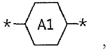
- According to an embodiment, there is provided a liquid crystal composition, including: at least one compound represented by Formula 1-A:

- R-* is *-H, *-F, *-Cl, *-Br, *-I, a C1-12 alkyl group, or a cyano group, and
- R1-* is a C1-12 alkyl group;
- Q-* is *-H or a C1-5 alkyl group;
- *-Z1-* and *-Z2-* are the same or different and are each independently *-O-*, *-COO-*, *-OCO-*, *-CF2O-*, *-OCF2-*, *-CH2O-*, *-OCH2-*, *-SCH2-*, *-CH2S-*, *-C2F4-*, *-CH2CF2-*, *-CF2CH2-*, *-(CH2)m-* (wherein m is an integer of 1 to 5), *-CH=CH-*, *-CF=CF-*, *-CH=CF-*, *-CF=CH-*, *-C≡C-*, *-CH=CHCH2O-*, or a single bond;


- n1 and n2 are each independently an integer of 0 to 3;
- n3 is an integer of 1 to 3;
- n4 is an integer of 1 or 2; and
- L1-*, L2-*, L3-*, L4-*, L5-*, L6-*, L7-*, and L8-* are the same or different and are each independently *-H, *-F, *-Cl, *-OCF3, *-CF3, *-CH2F, or *-CHF2.
- In the Formula 1-A,
- Q-* may be *-H, and
- n4 may be an integer of 1.
- In the Formula 1-A,
- Q-* may be *-H, and
- n3 may be an integer of 2.
- In the Formula 1-A,


- *-Z1-* and *-Z2-* may each be a single bond.
- In an embodiment, the at least one compound represented by Formula 1-A may be a compound represented by Formula 1-B:


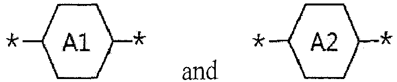
A1 A2, L1-* L2-*, L3-*, L4-*, L5-*, L6-*, L7-*, L8-*, R-*, R1-*, *-Z1-*, *-Z2-*, n1, and n2 are the same as in the Formula 1-A. - In an embodiment, the at least one compound represented by Formula 1-A may be a compound represented by Formulae 1-1 to 1-4:


- In an embodiment, the liquid crystal composition may further include at least one compound represented by Formulae 2-1 to 2-17:


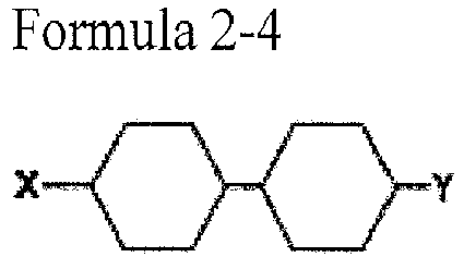


X-* and Y-* are each independently a C1-5 alkyl group. - In an embodiment, the content of at least one compound represented by Formula P may be 0 percent by weight:

- L11-* L21-*, L31-*, L41-*, L51-*, L61-*, L71-*, L81-*, L91-*, L101-*, L111-*, and L121-* are the same or different and are each independently H-* or F-*; and
- R11-* and R12-* are the same or different and are each independently a C1-5 alkyl group or a C1-5 alkoxy group.
- In an embodiment, the liquid crystal composition may have a refractive index anisotropy (Δn) of 0.08 to 0.12, a dielectric anisotropy (Δε) of -2.8 to -5.5, and a rotational viscosity (γ1, 20°C) of 70 millipascal seconds (mPa)·s to 140 millipascal seconds (mPa·s).
- In an embodiment, the content of the at least one compound represented by Formula 1-A may be about 1 percent by weight to about 10 percent by weight based on the total weight of the liquid crystal composition. For example, in an embodiment wherein the liquid crystal composition comprises more than one compound represented by Formula 1-A, the content of each compound represented by Formula 1-A may be about 1 percent by weight to about 10 percent by weight based on the total weight of the liquid crystal composition.
- In an embodiment, the liquid crystal composition may further include at least one reactive mesogen represented by Formula RM:
- Formula RM
- P1-SP1-MG-SP2-P2
- wherein, in the Formula RM,
- P1-* and P2-* are the same or different and are each independently


- *-SP1-* is

- *-SP2-* is

- *-MG-* is

- wherein, in the


- group (*-(CH2)c-*, wherein c is an integer of 1 to 10), a C1-10 alkyleneoxy group
- (*-(CH2)d-O-*, wherein d is an integer of 1 to 10),


- *-Z-* is *-(CH2)e-* (wherein e is an integer of 0 to 12), and
- *-Ar-* is


- wherein, in the


- A-* is H-*, a C1-10 alkyl group, F-*, Cl-*, Br-*, I-*, *-OH, *-NH2, or CN-*.
- According to an embodiment, there is provided a liquid crystal display device, including:
- a display substrate including a first base substrate,
- a switching element disposed on the first base substrate, and
- a first electrode disposed on the switching element;
- a counter display substrate including a second base substrate and a second electrode disposed on the second base substrate and facing the display substrate; and
- a liquid crystal layer containing the above mentioned liquid crystal composition.
- According to an embodiment, there is provided a liquid crystal display device, including:
- a display substrate including a first base substrate,
- a switching element disposed on the first base substrate, and
- a first electrode disposed on the switching element;
- a counter display substrate including a second base substrate and a second electrode disposed on the second base substrate and facing the display substrate; and
- a liquid crystal layer containing at least one compound represented by Formula 1-A and a at least one reactive mesogen represented by Formula RM, wherein the liquid crystal layer is disposed between the display substrate and the counter display substrate:

- R-* is *-H, *-F, *-Cl, *-Br, *-I, a C1-12 alkyl group, or a cyano group, and
- R1-* is a C1-12 alkyl group;
- Q-* is *-H or a C1-5 alkyl group;
- *-Z1-* and *-Z2-* are the same or different and are each independently *-O-*, *-COO-*, *-OCO-*, *-CF2O-*, *-OCF2-*, *-CH2O-*, *-OCH2-*, *-SCH2-*, *-CH2S-*, *-C2F4-*, *-CH2CF2-*, *-CF2CH2-*, *-(CH2)m-* (wherein m is an integer of 1 to 5), *-CH=CH-*, *-CF=CF-*, *-CH=CF-*, *-CF=CH-*, *-C≡C-*, *-CH=CHCH2O-*, or a single bond;


- n1 and n2 are each independently an integer of 0 to 3;
- n3 is an integer of 1 to 3;
- n4 is an integer of 1 or 2; and
- L1-*, L2-*, L3-*, L4-*, L5-*, L6-*, L7-*, and L8-* are the same or different and are each independently *-H, *-F, *-Cl, *-OCF3, *-CF3, *-CH2F, or *-CHF2;
- Formula RM
- P1-SP1-MG-SP2-P2
- wherein, in the Formula RM,
- P1-* and P2-* are the same or different and are each independently


- *-SP1-* is

- *-SP2-* is

- *-MG-* is

- wherein, in the


- *-Z-* is *-(CH2)e-* (wherein e may be an integer of 0 to 12), and
- *-Ar-* may be


- A-* is H-*, C1-10 alkyl group, F-*, Cl-*, Br-*, I-*, *-OH, *-NH2, or CN-*.
- In the Formula 1-A,
- Q-* may be *-H, and
- n4 may be an integer of 1.
- In the Formula 1-A,
- Q-* may be *-H, and
- n3 may be an integer of 2.
- In the Formula 1-A,


- In an embodiment, the at least one compound represented by Formula 1-A may be a compound represented by Formula 1-B:

A1 A2, L1-*, L2-*, L3-*, L4-*, L5-*, L6-*, L7-*, L8-*, R-* R1-*, *-Z1-* *-Z2-*, n1, and n2 are the same as in the Formula 1-A. - In an embodiment, the liquid crystal display device may further include
a liquid crystal alignment layer including a polymer of the reactive mesogen,
wherein the liquid crystal alignment layer is disposed between the liquid crystal layer and at least one of the display substrate and the counter display substrate. - In an embodiment, the at least one compound represented by Formula 1-A may be a compound represented by Formulae 1-1 to 1-4:


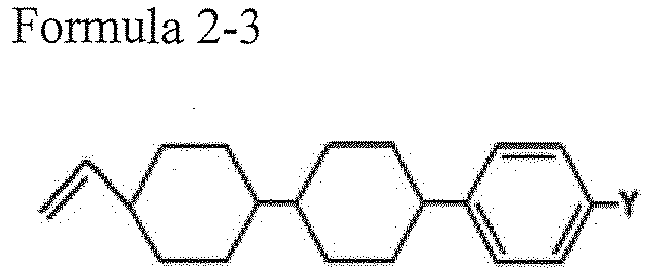
- In an embodiment, the liquid crystal layer may further include at least one compound represented by Formulae 2-1 to 2-17:




- In an embodiment, the content of at least one compound represented by Formula P may be 0 percent by weight:

- L11-* L21-*, L31-*, L41-*, L51-*, L61-*, L71-*, L81-*, L91-*, L101-*, L111-*, and L121-* are the same or different and are each independently H-* or F-*; and
- R11-* and R12-* are the same or different and are each independently a C1-5 alkyl group or a C1-5 alkoxy group.
- In an embodiment, the content of the at least one compound represented by Formula 1-A is about 1 percent by weight to about 10 percent by weight based on the total weight of the liquid crystal layer.
- As described below, according to the present disclosure, there is provided a low-viscosity liquid crystal composition having high reliability and a liquid crystal display device including the same.
- At least some of the above and other features of the invention are set out in the claims.
- The above and other aspects and features of the present disclosure will become more apparent by describing in detail embodiments thereof with reference to the attached drawings, in which:
-
FIG. 1 is a schematic exploded perspective view of a first liquid crystal display device; -
FIG. 2 is a schematic cross-sectional view of the initial state of the first liquid crystal display device ofFIG. 1 , to which an electric field is not applied; -
FIG. 3 is a diagram comparing the voltage holding rates and residual reactive mesogen contents according to fluorescence reaction of the liquid crystal compositions of Examples (the first liquid crystal composition - Mixture 1) with those of the liquid crystal composition of Comparative Examples (the comparative liquid crystal composition - Ref); -
FIG. 4 is a graph of light transmittance (percent, %) versus voltage (volts, V) comparing the measurement results of light transmittance of the liquid crystal cells containing the liquid crystal compositions of Examples (the second liquid crystal composition - Mixture 2) with those of the liquid crystal cell containing the liquid crystal composition of Comparative Examples (the comparative liquid crystal composition - Ref); -
FIG. 5 is a schematic cross-sectional view of the initial state of a second liquid crystal display device, to which an electric field is not applied; and -
FIG. 6 is a schematic cross-sectional view of the initial state of a third liquid crystal display device, to which an electric field is not applied. - Features of the inventive concept and methods of accomplishing the same may be understood more readily by reference to the following detailed description of embodiments and the accompanying drawings.
- The inventive concept may, however, be embodied in many different forms and should not be construed as being limited to the embodiments set forth herein. Rather, these embodiments are provided so that this disclosure will be thorough and complete and will fully convey the concept of the inventive concept to those skilled in the art, and the inventive concept will only be defined by the appended claims.
- In the drawings, the thickness of layers and regions are exaggerated for clarity. It will be understood that when an element or layer is referred to as being "on," "connected to" or "coupled to" another element or layer, the element or layer can be directly on, connected or coupled to another element or layer or intervening elements or layers. In contrast, when an element is referred to as being "directly on," "directly connected to" or "directly coupled to" another element or layer, there are no intervening elements or layers present. As used herein, connected may refer to elements being physically, electrically and/or fluidly connected to each other.
- Like numbers refer to like elements throughout. As used herein, the term "and/or" includes any and all combinations of one or more of the associated listed items.
- It will be understood that, although the terms first, second, third, etc., may be used herein to describe various elements, components, regions, layers and/or sections, these elements, components, regions, layers and/or sections should not be limited by these terms. These terms are only used to distinguish one element, component, region, layer or section from another element, component, region, layer or section. Thus, a first element, component, region, layer or section discussed below could be termed a second element, component, region, layer or section without departing from the teachings of the disclosure.
- Spatially relative terms, such as "bottom," "below," "lower," "under," "above," "upper," "top" and the like, may be used herein for ease of description to describe the relationship of one element or feature to another element(s) or feature(s) as illustrated in the figures. It will be understood that the spatially relative terms are intended to encompass different orientations of the device in use or operation, in addition to the orientation depicted in the figures. For example, if the device in the figures is turned over, elements described as "below" or "beneath" relative to other elements or features would then be oriented "above" relative to the other elements or features. Thus, the term "below" can encompass both an orientation of above and below. The device may be otherwise oriented (rotated 90 degrees or at other orientations) and the spatially relative descriptors used herein interpreted accordingly.
- The terminology used herein is for the purpose of describing particular embodiments only and is not intended to be limiting. As used herein, the singular forms "a," "an" and "the" are intended to include the plural forms as well, unless the context clearly indicates otherwise. It will be further understood that the terms "comprises," "comprising," "includes" and/or "including," when used in this specification, specify the presence of stated features, integers, operations, elements, and/or components, but do not preclude the presence or addition of one or more other features, integers, steps, operations, elements, components, and/or groups thereof.
- "About" or "approximately" as used herein is inclusive of the stated value and means within an acceptable range of deviation for the particular value as determined by one of ordinary skill in the art, considering the measurement in question and the error associated with measurement of the particular quantity (i.e., the limitations of the measurement system). For example, "about" can mean within one or more standard deviations, or within ± 30%, 20%, 10%, 5% of the stated value."
- Unless otherwise defined, all terms (including technical and scientific terms) used herein have the same meaning as commonly understood by one of ordinary skill in the art to which this disclosure belongs. It will be further understood that terms, such as those defined in commonly used dictionaries, should be interpreted as having a meaning that is consistent with their meaning in the context of the relevant art and the present disclosure, and will not be interpreted in an idealized or overly formal sense unless expressly so defined herein.
- Embodiments are described herein with reference to cross section illustrations that are schematic illustrations of these embodiments. As such, variations from the shapes of the illustrations as a result, for example, of manufacturing techniques and/or tolerances, are to be expected. Thus, embodiments described herein should not be construed as limited to the particular shapes of regions as illustrated herein but are to include deviations in shapes that result, for example, from manufacturing. For example, a region illustrated or described as flat may, typically, have rough and/or nonlinear features. Moreover, sharp angles that are illustrated may be rounded. Thus, the regions illustrated in the figures are schematic in nature and their shapes are not intended to illustrate the precise shape of a region and are not intended to limit the scope of the present claims.
- As used herein, when a definition is not otherwise provided, the term "alkyl group" refers to a group derived from a straight or branched chain saturated aliphatic hydrocarbon having the specified number of carbon atoms and having a valence of at least one.
- As used herein, when a definition is not otherwise provided, the term "alkoxy group" refers to "alkyl-O-", wherein the term "alkyl" has the same meaning as described above.
- As used herein, when a definition is not otherwise provided, the term "alkylene group" refers to a straight or branched saturated aliphatic hydrocarbon group having a valence of at least two, optionally substituted with one or more substituents.
- As used herein, when a definition is not otherwise provided, the term "alkyleneoxy group" refers to "alkylene-O-" or "-O-alkylene", wherein the term "alkylene" has the same meaning as described above.
- In the present specification, the "CA-B" means that the number of carbon atoms is equal to or more than A and equal to or less than B. In the present specification, the "A to B" is defined as equal to or more than A and equal to or less than B. In the present specification, the symbol "*" is defined as a bonding site in which adjacent elements are covalently bonded to each other. For example, an ethoxy group is a monovalent atomic group in which each of a methyl group (CH3-*) and an ether group (*-O-*) is bonded to methylene (*-CH2-*) and is represented by CH3-CH2-O-*, and ethyl methyl ether is a compound in which each of an ethyl group (CH3-CH2-*) and a methyl group (CH3-*) is bonded to an ether group (*-O-*) and is represented by CH3-CH2-O-CH3.
-
FIG. 1 is a schematic exploded perspective view of a liquidcrystal display device 500 including a display substrate SUB1 and a counter display substrate SUB2, andFIG. 2 is a schematic partial cross-sectional view of the display area I of the liquidcrystal display device 500 ofFIG. 1 . - Referring to
FIG. 1 , the liquidcrystal display device 500 may be configured to include: a display substrate SUB1; a counter display substrate SUB2 disposed to face the display substrate SUB1, and may be spaced apart from the display substrate SUB1 while maintaining a predetermined distance; and aliquid crystal layer 300 disposed between the display substrate SUB1 and the counter display substrate SUB2. Theliquid crystal layer 300 may include liquidcrystal compound molecules 301, and the liquidcrystal compound molecules 301 may have negative dielectric anisotropy. - The liquid
crystal display device 500 includes a display area I and a non-display area II. The display area I is an area in which an image is displayed. The non-display area II is a peripheral area surronding the display area I, and is an area in which an image is not displayed. - The display substrate SUB1 may include a plurality of gate lines GL extending in a first direction and a plurality of data lines DL extending in a second direction perpendicular to the first direction. Although not shown in the drawings, the gate lines GL are not disposed only in the display area I, and may extend to the non-display area II. In this case, the non-display area II may be provided with a gate pad (not shown). That is, in the non-display area II, the display substrate SUB1 may include a gate pad (not shown). Further, the data lines DL are not disposed only in the display area I, and may extend to the non-display area II. In this case, the non-display area II may be provided with a data pad (not shown). That is, in the non-display area II, the display substrate SUB1 may include a data pad (not shown).
- A plurality of pixels PX defined by the gate lines GL the data lines DL may be disposed in the display area I. The plurality of pixels PX may be arranged in the form of a matrix, and a
first electrode 180 may be disposed for each of the pixels PX. In this case, in the display area I, the display substrate SUB1 may include the plurality of pixels PX arranged in the form of a matrix and the plurality offirst electrodes 180 arranged in the form of a matrix. - In the non-display area II, a drive unit (not shown) for providing a gate drive signal and a data drive signal to each of the pixels PX may be disposed. In this case, in the non-display area II, the display substrate SUB1 may include a drive unit (not shown). The drive unit (not shown) may generate a gate drive signal and a data drive signal corresponding to a drive frequency of 120 Hertz (Hz) or more.
- The display substrate SUB1 may include a switching element array substrate (not shown) and a first electrode (not shown), and the counter display substrate SUB2 may include a second base substrate (not shown) and a second electrode (not shown). Hereinafter, the display substrate SUB1, the counter display substrate SUB2, and the
liquid crystal layer 300 will be described in more detail with reference toFIGS. 1 and2 . - Referring to
FIGS. 1 and2 , the display substrate SUB1 may be configured to include a switchingelement array substrate 100 and afirst electrode 180. The switchingelement array substrate 100 may be configured to include afirst base substrate 110, a switching element TFT disposed on thefirst base substrate 110, acolor filter layer 160 disposed on the switching element TFT, and anorganic film 170 disposed on thecolor filter layer 160. - The counter display substrate SUB2, which is a counter substrate of the display substrate SUB1, may be configured to include a
second base substrate 210 and asecond electrode 250. - The liquid
crystal display device 500 may further include a light-blockingspacer 195, a first liquidcrystal alignment layer 190, and a second liquidcrystal alignment layer 270. The light-blockingspacer 195 may be disposed between thefirst electrode 180 and thesecond electrode 250, and may include an area overlapping the switching element TFT. The light-blockingspacer 195 serves as both a spacer for maintaining the thickness of theliquid crystal layer 300 and a black matrix. The first liquidcrystal alignment layer 190 may be disposed on the display substrate SUB1, and may include an area disposed between thefirst electrode 180 and theliquid crystal layer 300. The second liquidcrystal alignment layer 270 may include an area disposed between thesecond electrode 250 and theliquid crystal layer 300. Further, the first liquidcrystal alignment layer 190 may include an area disposed between the light-blockingspacer 195 and the second liquidcrystal alignment layer 270, and the second liquidcrystal alignment layer 270 may include an area disposed between the first liquidcrystal alignment layer 190 and thesecond electrode 250. - The liquid
crystal display device 500 is realized by a polymer stabilized-vertical alignment mode (PS-VA mode). The PS-VA mode, which is a technology for stabilizing the pretilt alignment of liquidcrystal compound molecules 301 through a polymer network composed of polymers of reactive mesogens, may be performed by a first method and a second method to be described in detail later. - In the first method, vertical alignment films not containing the reactive mesogens (hereinafter, referred to as "N vertical alignment films") face each other, the liquid crystal composition containing the reactive mesogens is disposed between the N vertical alignment films to form a liquid crystal cell, and then the liquid crystal cell is exposed to ultraviolet rays in an electric field, thereby forming the polymer network on the N vertical alignment films.
- In the second method, vertical alignment films containing the reactive mesogens (hereinafter, referred to as "RM vertical alignment films") are formed on at least one electric field generating electrode of the
first electrode 180 and thesecond electrode 250 using the liquid crystal aligning agent containing the reactive mesogens, the liquid crystal composition is disposed between the RM vertical alignment films to form a liquid crystal cell, and then the liquid crystal cell is heat-treated to elute the reactive mesogens from the RM vertical alignment films to the liquid crystal composition, and then the heat-treated liquid crystal cell is exposed to ultraviolet rays, thereby forming the polymer network on the RM vertical alignment films. In this case, the reactive mesogens may be added to the liquid crystal composition, and may not be added thereto. - The reactive mesogen is a compound having a mesogenic structure for expressing liquid crystallinity and a polymerizable end group for polymerization. For example, the reactive mesogen may be represented by Formula RM below.
- Formula RM
- P1-SP1-MG-SP2-P2
- In the Formula RM, P1-* and P2-* may be each independently


- In the Formula RM, *-SP1-* may be
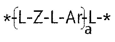


- In the


- In the

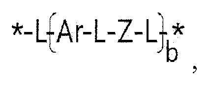


- In the


- The reactive mesogen, for example, may be at least one compound represented by Formula RM1 below.

- In the Formula RM1, Pm1-* and Pm2-* may be each independently


- In the Formula RM1, each of A1-* and A2-* may be *-H, *-F, *-Cl, Br-*, *-I, *-OH, *-NH2, or *-CN. A1-* and A2-* may be the same as or different from each other.
- Meanwhile, both the first method and the second method require an ultraviolet exposure process for polymerizing the reactive mesogens. Therefore, it is preferred that the
liquid crystal layer 300 is composed of the liquidcrystal compound molecules 301 having excellent photostability. - The ultraviolet exposure process may be performed using ultraviolet rays having a wavelength of about 300 nanometers (nm) or more. A compound represented by Formula P below absorbs ultraviolet rays having a wavelength of about 260 nm to 380 nm. Therefore, the compound represented by Formula P below has poor stability to ultraviolet rays having a wavelength of about 260 nm to 380 nm. When the
liquid crystal layer 300 contains the compound represented by Formula P below, the voltage holding rate (VHR) is lowered, and line afterimage and stains are generated, thereby deteriorating the reliability of the first liquidcrystal display device 500. Therefore, it is preferable that theliquid crystal layer 300 does not contain the compound represented by Formula P.

- In the Formula P, L11-*, L21-*, L31-*, L41-*, L51-*, L61-*, L71-*, L81-*, L91-*, L101-*, L111-*, and L121-* may be each independently H-* or F-*, and L11-*, L21-*, L31-*, L41-*, L51-*, L61-*, L71-*, L81-*, L91-*, L101-*, L111-*, and L121-* may be the same as or different from each other. In the Formula P, R11-* and R12-* may be each independently a C1-5 alkyl group or a C1-5 alkoxy group, and R11-* and R12-* may be the same as or different from each other.
- For example, the compound represented by Formula P above may be at least one compound represented by Formulae P-1 and P-2 below.


- As described above, the counter display substrate SUB2 is a counter substrate of the display substrate SUB1, which includes the
second base substrate 210 and thesecond electrode 250. In this case, thesecond electrode 250 may be directly disposed on thesecond base substrate 210. The first liquidcrystal display device 500 may be configured such that the display substrate SUB1 includes thecolor filter layer 160 and the light-blockingspacer 195, and the counter display substrate SUB2 does not include a color filter and a black matrix. In this case, at the time of the ultraviolet exposure process, the exposure amount of ultraviolet light incident on theliquid crystal layer 300 increases, compared to the embodiment where the counter display substrate SUB2 is designed to have a structure including a color filter and a black matrix. Therefore, the first liquidcrystal display device 500 particularly has a problem of reliability deterioration due to the compound represented by Formula P above. Accordingly, it is preferable that the content of the compound represented by Formula P above in theliquid crystal layer 300 is 0 percent by weight. - Meanwhile, in the polymer stabilized-vertical alignment mode, the compound represented by Formula P above serves to promote the polymerization reaction of the reactive mesogens. Therefore, in order to realize the first liquid
crystal display device 500 in the polymer stabilized-vertical alignment mode, a novel liquid crystal compound capable of promoting the polymerization reaction of the reactive mesogens is desired instead of the compound represented by Formula P above. - The
liquid crystal layer 300 may contain a compound represented by Formula 1-A below instead of the compound represented by Formula P above.

- In the Formula 1-A,


- In the Formula 1-A, n1 and n2 are each independently an integer of 0 to 3, n3 is an integer of 1 to 3, n4 is an integer of 1 or 2, and L1-*, L2-*, L3-*, L4-*, L5-*, L6-*, L7-*, and L8-* are each independently *-H, *-F, *-Cl, *-OCF3, *-CF3, *-CH2F, and *-CHF2. L1-*, L2-*, L3-*, L4-*, L5-*, L6-*, L7-*, and L8-* may be the same as or different from each other.
- In the Formula 1-A, Q-* may be *-H and n4 may be an integer of 1. In the Formula 1-A, Q-* may be *-H, and n3 may be an integer of 2.
- In the Formula 1-A,


- In an embodiment, the at least one compound represented by Formula 1-A may be a compound represented by Formula 1-B:

- The compound represented by Formula 1-A above has a benzofuran alkyl ether structure. Due to the benzofuran alkyl ether structure, the compound represented by Formula 1-A above has high refractive index characteristics, high electric constant characteristics, and high phase transition temperature (Tni), compared to a comparative compound not having the benzofuran alkyl ether structure. Therefore, when the comparative compound is replaced by the compound represented by Formula 1-A above, a liquid crystal composition having a high refractive index, a dielectric constant, and a high phase transition temperature can be prepared.
- Further, when the compound represented by Formula P above is replaced by the compound represented by Formula 1-A above, the compound represented by Formula 1-A above can promote the polymerization reaction of the reactive mesogens, and thus black afterimages of the first liquid
crystal display device 500 can be improved. That is, the compound represented by Formula 1-A above can improve the reliability of the first liquidcrystal display device 500. - The
liquid crystal layer 300 may contain the compound represented by Formula 1-A above in an amount of about 1 wt% to about 10 wt% based on the total weight of the liquid crystal composition. For example, in an embodiment wherein the liquid crystal layer comprises more than one compound represented by Formula 1-A, the content of each compound represented by Formula 1-A may be about 1 percent by weight to about 10 percent by weight, or about 2 percent by weight to about 8 percent by weight based on the total weight of the liquid crystal layer. When the content of the compound represented by Formula 1-A above is more than about 10 wt%, high-temperature stability may be deteriorated due to crystallization. - The compound represented by the Formula 1-A above, for example, may be a compound represented by Formulae 1-1 to 1-4 below.


- The simulation results of the phase transition temperature (Tni), refractive index anisotropy (Δn), dielectric anisotropy (Δε) and rotational viscosity (γ1) of the compounds (BF1, BF2, BF3, and BF4) represented by the Formulae 1-1 to 1-4 are summarized in Table 1 below. The simulation results of the phase transition temperature (Tni), refractive index anisotropy (Δn), dielectric anisotropy (Δε) and rotational viscosity (γ1) of the comparative compounds (CC1, CC2, CC3, CC4, CC5, and CC6) are summarized in Table 2 below.
Table 1 Liquid Crystal Compound Structural Formula Tni (°C) Δε (ε∥ -ε⊥) Δn (ne - no) γ1 (mPa·s) BF1 
89 -9.20 0.178 270 BF2 
153.4 -13.22 0.179 780 BF3 
172.3 -12.74 0.245 774 BF4 
132.7 -10.70 0.317 612 Table 2 Liquid Crystal Compound Structural Formula Tni (°C) Δε (ε∥ -∥⊥) Δn (ne - no) γ1 (mPa·s) CC1 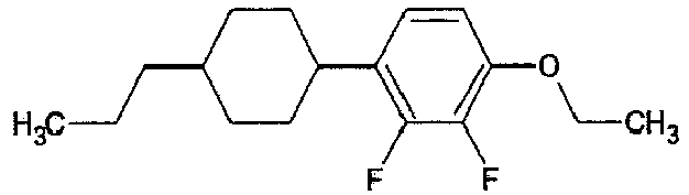
60.4 -4.94 0.106 72 CC2 
50.2 -5.12 0.157 70 CC3 
23.5 -5.15 0.000 12 CC4 
101.1 -6.12 0.083 474 CC5 
107.4 -6.05 0.158 464 CC6 
93.9 -3.10 0.244 276 - The results of measurement of the phase transition temperature (Tni), refractive index anisotropy (Δn), dielectric anisotropy (Δε), elastic modulus (K33) and rotational viscosity (γ1) of the liquid crystal compositions of Comparative Examples (hereinafter, referred to as "comparative liquid crystal compositions") not containing the compounds (BF1, BF2, BF3, and BF4) represented by the Formulae 1-1 to 1-4 are summarized in Table 3 below.
- The results of measurement of the phase transition temperature (Tni), refractive index anisotropy (Δn), dielectric anisotropy (Δε), elastic modulus (K33) and rotational viscosity (γ1) of the liquid crystal compositions of Examples (hereinafter, referred to as "first liquid crystal compositions") containing the compounds (BF1 and BF4) represented by the Formulae 1-1 and 1-4 are summarized in Table 4 below.
- The results of measurement of the phase transition temperature (Tni), refractive index anisotropy (Δn), dielectric anisotropy (Δε), elastic modulus (K33) and rotational viscosity (γ1) of the liquid crystal compositions of Examples (hereinafter, referred to as "second liquid crystal compositions") containing the compounds (BF1 and BF3) represented by the Formulae 1-1 and 1-3 are summarized in Table 5 below.
- The results of measurement of the phase transition temperature (Tni), refractive index anisotropy (Δn), dielectric anisotropy (Δε), elastic modulus (K33) and rotational viscosity (γ1) of the liquid crystal compositions of Examples (hereinafter, referred to as "third liquid crystal compositions") containing the compounds (BF1, BF2, BF3, and BF4) represented by the Formulae 1-1 to 1-4 are summarized in Table 6 below.
- In Tables 3 to 6,


- For example,


Table 3 Comparative Example Liquid crystal compound Content (wt%) Physical properties 1 2CC3 22 Tni(°C) : 75.5
Δ n (ne - no): 0.108
Δε (ε// - ε⊥): -3.0
K33: 13.0
γ 1 (mPa·s): 1202 3CCV4 9 3 3CPO1 7 4 3CAO2 15 5 4CCAO2 9.5 6 5CCAO2 5 7 2CPAO2 9 8 3CPAO2 9 9 2PAP3 7 10 3PAP4 7.5 Table 4 Example Liquid crystal compound Content (wt%) Physical properties 1 3CCV 10 Tni(°C): 76.5
Δ n(ne - no): 0.108
Δε (ε// - ε⊥): -3.0
K33 : 13.2
γ 1 (mPa·s): 952 3CCV1 15 3 VCCP1 5 4 2CC3 10 5 BF1 7 6 BF4 5 7 3CCP1 5 8 3CAO2 11 9 3PAO2 15 10 3CCAO2 8 11 2CCA1 5 12 2CPAO2 4 - Referring to Tables 3 and 4 above, each of the first liquid crystal compositions could ensure low-viscosity characteristics compared to the comparative liquid crystal compositions by replacing terphenyl liquid crystal compounds, such as 2PAP3 and 3PAP4, having poor stability to ultraviolet rays of about 260 nm to 380 nm with BF1 and BF4. Therefore, each of the first liquid crystal compositions can provide high-speed response characteristics to the first liquid
crystal display device 500.Table 5 Example Liquid crystal compound Content (wt%) Physical properties 1 3CCV 15 Tni(°C): 74.5
Δ n(ne - no): 0.108
Δε (ε// - ε⊥): -3.6
K33 : 14.0
γ 1 (mPa·s): 1152 3CCV1 10 3 2CC3 10 4 BF1 5 5 BF3 5 6 3CCP1 3 7 3CAO2 13 8 3PAO2 10 9 3CCAO2 8 10 2CCA1 5 11 2CPAO2 8 12 3CPAO2 8 - Referring to Tables 3 and 5 above, each of the second liquid crystal compositions could ensure high dielectric constant characteristics compared to the comparative liquid crystal compositions by replacing terphenyl liquid crystal compounds, such as 2PAP3 and 3PAP4, having poor stability to ultraviolet rays of about 260 nm to 380 nm with BF1 and BF3. Therefore, each of the second liquid crystal compositions can provide high-transmittance characteristics and low-voltage characteristics to the first liquid
crystal display device 500.Table 6 Example Liquid crystal compound Content (wt%) Physical properties 1 3CCV 15 Tni(°C): 100.0
Δ n(ne - no): 0.109
Δε (ε// - ε⊥): -3.5
K33 : 17.7
γ 1 (mPa·s): 1402 3CCV1 7 3 2CC3 7 4 3CC4 10 5 BF1 5 6 BF2 3 7 BF3 3 8 BF4 3 9 3CPO1 5 10 3CCP1 7 11 3CAO4 4 12 3CCAO2 15 13 2CPAO2 8 14 3CPAO2 8 - Referring to Tables 3 and 6 above, each of the third liquid crystal compositions could ensure high phase transition temperature and high dielectric constant characteristics compared to the comparative liquid crystal compositions by replacing terphenyl liquid crystal compounds, such as 2PAP3 and 3PAP4, having poor stability to ultraviolet rays of about 260 nm to 380 nm with BF1, BF2, BF3, and BF4.
- Meanwhile,
FIG. 3 shows a graph comparing the measurement results of the voltage holding rates and residual reactive mesogen contents according to fluorescence reaction of the first liquid crystal composition (Mixture 1) with those of the comparative liquid crystal composition (Ref.). The measurement results of the voltage holding rates are summarized in Table 7 below, and the measurement results of the residual reactive mesogen contents are summarized in Table 8 below. The voltage holding rates thereof were measured under the following conditions.
- Frame frequency: 60 Hz (16.64 milliseconds, ms)
- Pulse width: 64 microseconds (µs)
- Data voltage: 1 volts (V)
- Cell gap: 3.0 micrometers (µm)
- Exposure condition: 6 joules (J), 70 seconds (sec)Table 7 Voltage holding rate (%) Time Comparative liquid crystal composition (Ref.) First liquid crystal composition (Mixture 1) Initial (0 hr) After 168 hr (168 hr) Initial (0 hr) After 168 hr (168 hr) 0 min 99.32 99.44 99.21 99.45 20 min 99.18 99.29 99.13 99.34 40 min 98.94 99.19 99.06 99.21 60 min 98.56 99.05 98.94 99.21 80 min 98.35 98.87 98.95 99.07 100 min 98.12 98.63 98.85 99.14 Table 8 Residual reactive mesogen content according to fluorescence reaction (%) Time Comparative liquid crystal composition (Ref.) First liquid crystal composition (Mixture 1) 0 min 77..0 81.7 20 min 20.7 18.3 40 min 2.6 4.4 60 min 1.8 2.7 80 min 1.4 1.9 100 min 1.1 1.5 - Referring to Tables 7 and 8 and
FIG. 3 , the first liquid crystal composition increases a voltage holding rate, and promotes the polymerization reaction of the reactive mesogens, so as to pretilt the liquidcrystal compound molecules 301, by replacing terphenyl liquid crystal compounds, such as 2PAP3 and 3PAP4, having poor stability to ultraviolet rays of about 260 nm to 380 nm with BF1 and BF4. -
FIG. 4 show a graph comparing the measurement results of light transmittance of the liquid crystal cell (Mixture 2) containing the second liquid crystal composition with those of the liquid crystal cell (Ref.) containing the comparative liquid crystal composition. Referring toFIG. 4 , the liquid crystal cell containing the second liquid crystal composition (Mixture 2) could exhibit high-transmittance characteristics by 8% or more compared to the liquid crystal cell containing the comparative liquid crystal composition (Ref.). - Referring to
FIGS. 1 and2 again, thefirst base substrate 110 is a base substrate of the switchingelement array substrate 100, and may be made of a transparent insulating material, such as glass or transparent plastic. - The switching element TFT may be a thin film transistor, and the thin film transistor may be configured to include a
gate electrode 125, agate insulating film 130, asemiconductor layer 140, asource electrode 152, and adrain electrode 155. Thegate electrode 125, which is a control terminal of the thin film transistor, may be disposed on thefirst base substrate 110, and may be made of a conductive material. Thegate electrode 125 may be branched from the gate line GL. Thegate insulating film 130 may be disposed between thegate electrode 125 and thesemiconductor layer 140 to insulate them, and may be formed to extend from the display area I to the non-display area II. Thesemiconductor layer 140, which is a channel layer of the thin film transistor, may be disposed on thegate insulating film 130. Thesource electrode 152 and thedrain electrode 155 may be disposed on thesemiconductor layer 140 to be spaced from each other, and may be made of a conductive material. Thesource electrode 152 is an input terminal of the thin film transistor, and thedrain electrode 155 is an output terminal of the thin film transistor. Thesource electrode 152 and thedrain electrode 155 may be branched from the data line DL. Ohmic contact layers (not shown) may be respectively formed between thesource electrode 152 and thesemiconductor layer 140 and between thedrain electrode 155 and thesemiconductor layer 140. - The gate line GL may be disposed between the
first base substrate 110 and thefirst electrode 180, and the data line DL may be disposed between the gate line GL and thefirst electrode 180. - The
color filter layer 160 may be formed on thesource electrode 152 and thedrain electrode 155. Thecolor filter layer 160 may be disposed on the switching element TFT, for example, may be disposed between the switching element TFT and thefirst electrode 180. Thecolor filter layer 160 may be formed in a region corresponding to each pixel PX in the display area I, wherein thecolor filter layer 160 includes a first color filter 160-1 and a second color filter 160-2. For example, the first color filter 160-1 and the second color filter 160-2 may be color filters realizing different colors from each other. Each of the first color filter 160-1 and the second color filter 160-2 may be one of a red color filter (R), a green color filter (G), and a blue color filter (B). The first color filter 160-1 and the second color filter 160-2 may be arranged alternately. - The
organic film 170 made of an organic material may be formed on thecolor filter layer 160. Theorganic film 170 may extend to the non-display area II. - On the
organic film 170, thefirst electrode 180 made of a conductive material may be formed for each pixel PX. Thefirst electrode 180 may be electrically connected with thedrain electrode 155 through a contact hole penetrating theorganic film 170 and thecolor filter layer 160. The switching element TFT is electrically connected to the gate line GL and thef electrode 180. Thefirst electrode 180 may be made of indium tin oxide, indium zinc oxide, indium oxide, zinc oxide, tin oxide, gallium oxide, titanium oxide, aluminum, silver, platinum, chromium, molybdenum, tantalum, niobium, zinc, magnesium, an alloy thereof, or a laminate thereof. Thefirst electrode 180 is disposed between thecolor filter layer 160 and theliquid crystal layer 300. - The
first electrode 180 forms an electric field together with thesecond electrode 250 to control the alignment direction of liquid crystal molecules in theliquid crystal layer 300 disposed therebetween. Thefirst electrode 180 may be a pattern electrode having at least one of a protrusion pattern and a slit pattern, or may be a patternless electrode. - The light-blocking
spacer 195 may be disposed on the display substrate SUB1. In an embodiment, the light-blockingspacer 195 may include an area disposed between thefirst electrode 180 and thesecond electrode 250, and an area disposed to overlap the switching element TFT. The light-blockingspacer 195 serves as both a spacer for maintaining the thickness of theliquid crystal layer 300 and a black matrix. The light-blockingspacer 195 may be made of a light-blocking material, such as an organic material containing carbon black. The light-blocking material may also be made of a material having predetermined elasticity. The light-blockingspacer 195 serves as both a black matrix and a spacer for maintaining the thickness of theliquid crystal layer 300. The light-blockingspacer 195, for example, may include amain spacer 195M and asub spacer 195S. Themain spacer 195M is formed to have a height higher than that of the subs spacer 195S, and can serve to maintain the thickness of theliquid crystal layer 300 even when external force is applied to the liquidcrystal display device 500. Thesub spacer 195S can serve to prevent the elasticity of themain spacer 195M from being destroyed by buffering the external force applied to themain spacer 195M when the external force is stronger than the elasticity of themain spacer 195M. The height difference t1-t2 between themain spacer 195M and thesub spacer 195S may be 0.25 µm to 0.8 µm. For example, when themain spacer 195M has a thickness t1 of 3 µm, thesub spacer 195S may have a thickness t2 of 2.5 µm. - The first liquid
crystal alignment layer 190 may include an area disposed between thefirst electrode 180 and theliquid crystal layer 300 and an area disposed between the light-blockingspacer 195 and the second liquidcrystal alignment layer 270. The first liquidcrystal alignment layer 190 may include a polymer network composed of polymers of the reactive mesogens, and, for example, may include a polymer network composed of polymers of one or more reactive mesogens of the compound represented by Formula RM1. - The polymer network composed of polymers of the reactive mesogens serves to align the liquid
crystal compound molecules 301 at a predetermined pretilt angle with respect to the display substrate SUB1 and the counter display substrate SUB2 even in a state where an electric field is not applied to the first liquidcrystal display device 500. The pretilt angle means an angle between the display substrate SUB 1 and the director of the liquidcrystal compound molecules 301 and an angle between the counter display substrate SUB2 and the director of the liquidcrystal compound molecules 301. - Although not shown in the drawings, the first liquid
crystal alignment layer 190 includes a polyimide alignment base layer and the polymer network composed of polymers of the reactive mesogens, and may further include an alignment stabilizing layer formed on the polyimide alignment base layer. However, since the polyimide alignment base layer may be emitted, the first liquidcrystal alignment layer 190 may not include both the polyimide alignment base layer and the alignment stabilizing layer. - The
second base substrate 210 is a base substrate of the counter display substrate SUB2, and may be made of a transparent insulating material, such as glass or transparent plastic. - The
second electrode 250 may be directly disposed on thesecond base substrate 210. Thesecond electrode 250 may be a pattern electrode having at least one of a protrusion pattern and a slit pattern, or may be a patternless electrode. Thesecond electrode 250 may be made of indium tin oxide, indium zinc oxide, indium oxide, zinc oxide, tin oxide, gallium oxide, titanium oxide, aluminum, silver, platinum, chromium, molybdenum, tantalum, niobium, zinc, magnesium, an alloy thereof, or a laminate thereof. - The second liquid
crystal alignment layer 270 may be directly disposed on thesecond electrode 250. The second liquidcrystal alignment layer 250 may include an area disposed between thesecond electrode 250 and theliquid crystal layer 300 and an area disposed between thesecond electrode 250 and the first liquidcrystal alignment layer 190. The second liquidcrystal alignment layer 270 may extend to the non-display area II as well as the display area I. The second liquidcrystal alignment layer 270 may include a polymer network composed of polymers of the reactive mesogens, and, for example, may include a polymer network composed of polymers of one or more reactive mesogens of the compound represented by Formula RM1. - The polymer network composed of polymers of the reactive mesogens serves to align the liquid
crystal compound molecules 301 at a predetermined pretilt angle with respect to the display substrate SUB1 and the counter display substrate SUB2 even in a state where an electric field is not applied to the first liquidcrystal display device 500. The pretilt angle means an angle between the display substrate SUB1 and the director of the liquidcrystal compound molecules 301 and an angle between the counter display substrate SUB2 and the director of the liquidcrystal compound molecules 301. - Although not shown in the drawings, the second liquid
crystal alignment layer 270 includes a polyimide alignment base layer and the polymer network composed of polymers of the reactive mesogens, and may further include an alignment stabilizing layer formed on the polyimide alignment base layer. However, since the polyimide alignment base layer may be emitted, the second liquidcrystal alignment layer 270 may not include both the polyimide alignment base layer and the alignment stabilizing layer. - Although not shown in the drawing, the first liquid
crystal display device 500 may further include a backlight assembly (not shown) disposed on the rear surface of the display substrate SUB1 to provide light to theliquid crystal layer 300. - The backlight assembly, for example, may include a light guide plate (not shown), a light source (not shown), a reflection member (not shown), and an optical sheet (not shown).
- The light guide plate (LGP) serves to change the path of light emitted from the light source toward the
liquid crystal layer 300, and may include a light incidence surface provided to allow the light emitted from the light source to be applied thereto, and a light emission surface emitting the incident light toward theliquid crystal layer 300. The light guide plate may be made of a material having a predetermined refractive index, such as polymethyl methacrylate (PMMA) or polycarbonate (PC), which is one of light transmissive materials, but the present disclosure is not limited thereto. - Since the light incoming onto one side or both sides of the light guide plate made of such a material has an angle within the critical angle, the light is transmitted to the inside of the light guide plate. Further, when the light incomes to the upper surface or lower surface of the light guide plate, the angle of the light exceeds the critical angle, so that the light is not emitted to the outside of the light guide plate, and is uniformly transmitted in the light guide plate.
- A scattering pattern may be formed on any one of the upper and lower surfaces of the light guide plate, for example, on the upper surface facing the light emission surface, such that the guided light is emitted to the upper surface thereof. That is, the scattering pattern may be printed with ink on one side of the light guide plate such that the light transmitted in the light guide plate is emitted to the upper surface thereof. Such a scattering pattern may be formed by printing with ink, but is not limited thereto. Further, the light guide plate may be provided with fine grooves or protrusions, and may be modified as desired.
- The reflection member may further be provided between the light guide plate and the bottom of the storage member. The reflection member serves to reflect the light emitted to the lower surface of the light guide plate, that is, the opposite surface facing the light emission surface and supply the reflected light to the light guide plate. The reflection member may be fabricated in the form of a film, but the present disclosure is not limited thereto.
- The light source may be disposed to face the light incidence surface of the light guide plate. The number of light sources can be appropriately changed as needed. For example, only one side of the light guide plate can be provided with one light source, and three or more light sources can also be provided corresponding to three or more sides of four sides of the light guide plate. Further, a plurality of light sources can be provided corresponding to any one of sides of the light guide plate. As described above, the side light type light source has been described as an example, but other examples thereof include a direct type light source and a surface shape type light source.
- The light source may be a white LED emitting white light, and may also be a plurality of LEDs emitting red light (R), green light (G), and blue light (B), respectively. When the plurality of light sources are realized as the plurality of LEDs emitting red light (R), green light (G), and blue light (B), respectively, and when these light sources turn on at once, white light can be realized by color mixing.
-
FIG. 5 is a schematic cross-sectional view of the initial state of a second liquid crystal display device 500', to which an electric field is not applied. Hereinafter, the second liquid crystal display device 500' will be described except for the portions similar to the first liquid crystal display device (500 ofFIG. 2 ). - The second liquid crystal display device 500' is different from the first liquid
crystal display device 500 ofFIG. 2 in that a counter display substrate SUB2 is configured to include asecond base substrate 210, a light-blockingpattern 220, and asecond electrode 250. The counter display substrate SUB2 of the first liquidcrystal display device 500 ofFIG. 2 is configured to include thesecond base substrate 210 and thesecond electrode 250. The second liquid crystal display device 500' does not include the light-blocking spacer (195 ofFIG. 2 ). Although not shown, the second liquid crystal display device 500' may further include a column spacer (not shown) for maintaining the thickness of theliquid crystal layer 300, and the spacer may be made of a light transmissive material. The display substrate SUB 1 and the counter display substrate SUB2 may be attached to each other by aseal line 310 made of a sealant. Theseal line 310, which is a peripheral portion of the display substrate SUB 1 and the counter display substrate SUB2, may be located on the non-display area (II). Theseal line 310 surrounds the display area (I). - As described above, since the compound represented by Formula P above has poor stability to ultraviolet rays of about 260 nm to 380 nm, the reliability of the second liquid crystal display device 500' can be improved by partially or entirely replacing the compounds represented by Formula P above with at least one of the compounds represented by the Formula 1-A.
-
FIG. 6 is a schematic cross-sectional view of the initial state of a third liquidcrystal display device 500", to which an electric field is not applied. Hereinafter, the third liquidcrystal display device 500" will be described except for the portions similar to the first liquid crystal display device (500 ofFIG. 2 ). - The third liquid
crystal display device 500" is different from the first liquidcrystal display device 500 ofFIG. 2 in that the switchingelement array substrate 100 is configured to include afirst base substrate 110, a switching element TFT disposed on thefirst base substrate 110, an inorganic film 160' disposed on the switching element TFT, and anorganic film 170 disposed on the inorganic film 160'. The switchingelement array substrate 100 of the first liquidcrystal display device 500 ofFIG. 2 , for example, is configured to include thefirst base substrate 110, the switching element TFT disposed on thefirst base substrate 110, thecolor filter layer 160 disposed on the switching element TFT, and theorganic film 170 disposed on thecolor filter layer 160. - The third liquid
crystal display device 500" is different from the first liquidcrystal display device 500 ofFIG. 2 in that a counter display substrate SUB2 is configured to include asecond base substrate 210, a light-blockingpattern 220, anovercoat film 240, and asecond electrode 250. The counter display substrate SUB2 of the first liquidcrystal display device 500 ofFIG. 2 is configured to include thesecond base substrate 210 and thesecond electrode 250. - The third liquid
crystal display device 500" does not include the light-blocking spacer (195 ofFIG. 2 ). Although not shown, the third liquidcrystal display device 500" may further include a column spacer (not shown) for maintaining the thickness of theliquid crystal layer 300, and the spacer may be made of a light transmissive material. The display substrate SUB1 and the counter display substrate SUB2 may be attached to each other by aseal line 310 made of a sealant. Theseal line 310, which is a peripheral portion of the display substrate SUB 1 and the counter display substrate SUB2, may be located on the non-display area (II). Theseal line 310 surrounds the display area (I). - As described above, since the compound represented by Formula P above has poor stability to ultraviolet rays of about 260 nm to 380 nm, the reliability of the third liquid
crystal display device 500" can be improved by partially or entirely replacing the compounds represented by Formula P above with at least one of the compounds represented by the Formula 1-A. - While embodiments have been shown and described above, it will be apparent to those skilled in the art that modifications and variations could be made without departing from the scope of the disclosure as defined by the appended claims. The embodiments should be considered in a descriptive sense only and not for purposes of limitation.
Claims (21)
- A liquid crystal composition, comprising:at least one compound represented by Formula 1-A:
 R-* is *-H, *-F, *-Cl, *-Br, *-I, a C1-12 alkyl group, or a cyano group,R1-* is a C1-12 alkyl group;Q-* is *-H or a C1-5 alkyl group;*-Z1-* and *-Z2-* are the same or different and are each independently *-O-*, *-COO-*, *-OCO-*, *-CF2O-*, *-OCF2-*, *-CH2O-*, *-OCH2-*, *-SCH2-*, *-CH2S-*, *-C2F4-*, *-CH2CF2-*, *-CF2CH2-*, *-(CH2)m-* (wherein m is an integer of 1 to 5), *-CH=CH-* *-CF=CF-*, *-CH=CF-*, *-CF=CH-*, *-C≡C-* *-CH=CHCH2O-*, or a single bond;

 n1 and n2 are each independently an integer of 0 to 3; andn3 is an integer of 1 to 3;n4 is an integer of 1 or 2; andL1-*, L2-*, L3-*, L4-*, L5-*, L6-*, L7-*, and L8-* are the same or different and are each independently *-H, *-F, *-Cl, *-OCF3, *-CF3, *-CH2F, or *-CHF2.
 - A liquid crystal composition according to claim 1, whereinQ-* is *-H, andn4 is an integer of 1.
- A liquid crystal composition according to claim 1 or claim 2, whereinQ-* is *-H, andn3 is an integer of 2.
- A liquid crystal composition according to any one of claims 1 to 3, wherein


- A liquid crystal composition according to any one of claims 1 to 4, wherein the at least one compound represented by Formula 1-A is a compound represented by Formula 1-B:

A1, A2, L1-*, L2-*, L3-*, L4-*, L5-*, L6-*, L7-* L8-*, R-* R1-*, *-Z1-* *-Z2-*, n1, and n2 are the same as in the Formula 1-A. - A liquid crystal composition according to any one of claims 1 to 5, wherein the at least one compound represented by Formula 1-A is a compound represented by Formulae 1-1 to 1-4:


- A liquid crystal composition according to any one of claims 1 to 6, further comprising:at least one compound represented by Formulae 2-1 to 2-17:


X-* and Y-* are each independently a C1-5 alkyl group. - A liquid crystal composition according to any one of claims 1 to 7, wherein the content of at least one of compound represented by Formula P is 0 percent by weight:
 L11-*, L21-*, L31-*, L41-*, L51-*, L61-*, L71-*, L81-*, L91-*, L101-*, L111-*, and L121-* are the same or different and are each independently H-* or F-*; andR11-* and R12-* are the same or different and are each independently a C1-5 alkyl group or a C1-5 alkoxy group.
 - A liquid crystal composition according to any one of claims 1 to 8, wherein the liquid crystal composition has a refractive index anisotropy (Δn) of 0.08 to 0.12, a dielectric anisotropy (Δε) of -2.8 to -5.5, and a rotational viscosity (γ1, 20°C) of 70 millipascal seconds (mPa·s) to 140 millipascal seconds (mPa·s).
- A liquid crystal composition according to any one of claims 1 to 9, wherein the content of the at least one compound represented by Formula 1-A is about 1 percent by weight to about 10 percent by weight based on the total weight of the liquid crystal composition.
- A liquid crystal composition according to any one of claims 1 to 10, further comprising at least one reactive mesogen represented by Formula RM:Formula RMP1-SP1-MG-SP2-P2wherein, in the Formula RM,P1-* and P2-* are the same or different and are each independently

 *-SP1-* is
 *-PS2-* is
 *-MG-* is
 wherein, in the
 (*-(CH2)d-O-*, wherein d is an integer of 1 to 10),
 *-Z-* is *-(CH2)e-* (wherein e is an integer of 0 to 12), and*-Ar-* is

wherein, in the
 A-* is H-*, a C1-10 alkyl group, F-*, Cl-*, Br-*, I-*, *-OH, *-NH2, or CN-*.
 - A liquid crystal display device, comprising:a display substrate comprising a first base substrate, a switching element disposed on the first base substrate, and a first electrode disposed on the switching element;a counter display substrate comprising a second base substrate and a second electrode disposed on the second base substrate and facing the display substrate; anda liquid crystal layer comprising at least one compound represented by Formula 1-A and at least one reactive mesogen represented by Formula RM, wherein the liquid crystal layer is disposed between the display substrate and the counter display substrate:
 R-* is *-H, *-F, *-Cl, *-Br, *-I, a C1-12 alkyl group, or a cyano group,R1-* is a C1-12 alkyl group;Q-* is *-H or a C1-5 alkyl group;*-Z1-* and *-Z2-* are the same or different and are each independently *-O-*, *-COO-*, *-OCO-*, *-CF2O-*, *-OCF2-*, *-CH2O-*, *-OCH2-*, *-SCH2-*, *-CH2S-*, *-C2F4-*, *-CH2CF2-*, *-CF2CH2-*, *-(CH2)m-* (wherein m is an integer of 1 to 5), *-CH=CH-*, *-CF=CF-*, *-CH=CF-*, *-CF=CH-*, *-C≡C-*, *-CH=CHCH2O-*, or a single bond;

 n1 and n2 are each independently an integer of 0 to 3;n3 is an integer of 1 to 3;n4 is an integer of 1 or 2; andL1-*, L2-*, L3-*, L4-*, L5-*, L6-*, L7-*, and L8-* are the same or different and are each independently *-H, *-F, *-Cl, *-OCF3, *-CF3, *-CH2F, or *-CHF2;
Formula RM P1-SP1-MG-SP2-P2
wherein, in the Formula RM,P1-* and P2-* are the same or different and are each independently
 *-SP1-* is
 *-SP2-* is
 *-MG-* is
 wherein, in the


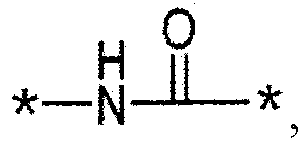 *-Z-* is *-(CH2)e-* (wherein e is an integer of 0 to 12), and*-Ar-* is

wherein, in the

- A liquid crystal display device according to claim 12, whereinQ-* is *-H, andn4 is an integer of 1.
- A liquid crystal display device according to claim 12 or claim 13, whereinQ-* is *-H, andn3 is an integer of 2.
- A liquid crystal display device according to any one of claims 12 to 14, wherein


- A liquid crystal display device according to any one of claims 12 to 15, wherein the at least one compound represented by Formula 1-A is a compound represented by Formula 1-B:

A1, A2, L1-*, L2-*, L3-*, L4-*, L5-*, L6-*, L7-*, L8-*, R-*, R1-*, *-Z1-*, *-Z2-*, n1, and n2 are the same as in the Formula 1-A. - A liquid crystal display device according to any one of claims 12 to 16, further comprising:a liquid crystal alignment layer comprising a polymer of the reactive mesogen,wherein the liquid crystal alignment layer is disposed between the liquid crystal layer and at least one of the display substrate and the counter display substrate.
- A liquid crystal display device according to any one of claims 12 to 17, wherein the at least one compound represented by Formula 1-A is a compound represented by Formulae 1-1 to 1-4:


- A liquid crystal display device according to any one of claims 12 to 18, wherein the liquid crystal layer further comprises at least one compound represented by Formulae 2-1 to 2-17:


X-* and Y-* are each independently a C1-5 alkyl group. - A liquid crystal display device according to any one of claims 12 to 19, wherein the content of at least one compound represented by Formula P is 0 percent by weight:
 L11-*, L21-*, L31-*, L41-*, L51-*, L61-*, L71-*, L81-*, L91-*, L101-*, L111-*, and L121-* are the same or different and are each independently H-* or F-*; andR11-* and R12-* are the same or different and are each independently a C1-5 alkyl group or a C1-5 alkoxy group.
 - A liquid crystal display device according to any one of claims 12 to 20, wherein the content of the at least one compound represented by Formula 1-A is about 1 percent by weight to about 10 percent by weight based on the total weight of the liquid crystal layer.
Applications Claiming Priority (2)
| Application Number | Priority Date | Filing Date | Title |
|---|---|---|---|
| KR20160043216 | 2016-04-08 | ||
| KR1020160097115A KR102539385B1 (en) | 2016-04-08 | 2016-07-29 | Liquid crystal composition and liquid crystal display device includig the same |
Publications (2)
| Publication Number | Publication Date |
|---|---|
| EP3228680A1 true EP3228680A1 (en) | 2017-10-11 |
| EP3228680B1 EP3228680B1 (en) | 2020-01-08 |
Family
ID=57218804
Family Applications (1)
| Application Number | Title | Priority Date | Filing Date |
|---|---|---|---|
| EP16196728.6A Active EP3228680B1 (en) | 2016-04-08 | 2016-11-01 | Liquid crystal composition and liquid crystal display device including the same |
Country Status (3)
| Country | Link |
|---|---|
| US (1) | US10640708B2 (en) |
| EP (1) | EP3228680B1 (en) |
| CN (1) | CN107267154B (en) |
Families Citing this family (5)
| Publication number | Priority date | Publication date | Assignee | Title |
|---|---|---|---|---|
| WO2018037356A1 (en) | 2016-08-23 | 2018-03-01 | Medicem Ophthalmic (Cy) Limited | Ophthalmic lenses with aspheric optical surfaces and method for their manufacture |
| KR102662829B1 (en) * | 2016-09-27 | 2024-05-03 | 티씨엘 차이나 스타 옵토일렉트로닉스 테크놀로지 컴퍼니 리미티드 | Liquid crystal composition and display device including the same |
| TWI613277B (en) * | 2016-11-02 | 2018-02-01 | Daxin Materials Corporation | Liquid crystal compound, liquid crystal composition and liquid crystal display using the same |
| CN109181712B (en) * | 2018-10-10 | 2021-08-20 | 西安近代化学研究所 | Benzofuran liquid crystal compound with difluoromethyl ether bridge bond and composition thereof |
| CN116948657B (en) * | 2023-06-28 | 2024-10-29 | 北京燕化集联光电技术有限公司 | Liquid crystal compound, composition and application thereof |
Citations (4)
| Publication number | Priority date | Publication date | Assignee | Title |
|---|---|---|---|---|
| DE19900517A1 (en) * | 1998-01-19 | 1999-07-22 | Merck Patent Gmbh | Difluorobenzofuran and dihydrodifluorobenzofuran derivatives of linear (poly)cyclic compounds |
| DE19909760A1 (en) * | 1998-04-17 | 1999-10-21 | Merck Patent Gmbh | New benzo(b)furan derivatives used as components of liquid crystal media for liquid crystal and electro-optical displays |
| WO2001021606A1 (en) * | 1999-09-21 | 2001-03-29 | Qinetiq Limited | Liquid crystal compounds |
| DE102004053279A1 (en) * | 2003-11-25 | 2005-06-23 | Merck Patent Gmbh | Benzofuran and benzothiophene derivatives, useful as components of liquid crystal media for electro-optical display devices are new |
Family Cites Families (6)
| Publication number | Priority date | Publication date | Assignee | Title |
|---|---|---|---|---|
| US5102578A (en) * | 1988-08-15 | 1992-04-07 | Hoffmann-La Roche Inc. | Liquid crystalline mixtures and method of making same |
| DE19909761A1 (en) | 1998-04-17 | 1999-10-21 | Merck Patent Gmbh | New optically inactive benzo(b)furan, benzo(1,2-b:4,5-b')difuran and benzo(1,2-b:5,4-b')difuran derivatives, used in liquid crystal media |
| CN100415730C (en) | 2002-12-06 | 2008-09-03 | 石家庄永生华清液晶有限公司 | Benzofuran derivative and its prepn and use |
| DE102005045849A1 (en) * | 2004-10-07 | 2006-04-20 | Merck Patent Gmbh | Preparation of benzocondensed oxyheterocycle, useful in liquid crystalline mixtures, comprises regioselective opening of e.g. oxetane by metallized fluoroaromates and cyclizing the obtained propanol derivative by non-nucleophilic base |
| DE102012024126A1 (en) * | 2011-12-20 | 2013-06-20 | Merck Patent Gmbh | Liquid crystalline medium |
| KR20180006522A (en) * | 2016-07-07 | 2018-01-18 | 삼성디스플레이 주식회사 | Liquid crystal composition and liquid crystal display including the same |
-
2016
- 2016-11-01 EP EP16196728.6A patent/EP3228680B1/en active Active
- 2016-11-10 CN CN201610991561.1A patent/CN107267154B/en active Active
-
2017
- 2017-01-06 US US15/400,199 patent/US10640708B2/en active Active
Patent Citations (4)
| Publication number | Priority date | Publication date | Assignee | Title |
|---|---|---|---|---|
| DE19900517A1 (en) * | 1998-01-19 | 1999-07-22 | Merck Patent Gmbh | Difluorobenzofuran and dihydrodifluorobenzofuran derivatives of linear (poly)cyclic compounds |
| DE19909760A1 (en) * | 1998-04-17 | 1999-10-21 | Merck Patent Gmbh | New benzo(b)furan derivatives used as components of liquid crystal media for liquid crystal and electro-optical displays |
| WO2001021606A1 (en) * | 1999-09-21 | 2001-03-29 | Qinetiq Limited | Liquid crystal compounds |
| DE102004053279A1 (en) * | 2003-11-25 | 2005-06-23 | Merck Patent Gmbh | Benzofuran and benzothiophene derivatives, useful as components of liquid crystal media for electro-optical display devices are new |
Also Published As
| Publication number | Publication date |
|---|---|
| CN107267154A (en) | 2017-10-20 |
| EP3228680B1 (en) | 2020-01-08 |
| CN107267154B (en) | 2022-03-15 |
| US10640708B2 (en) | 2020-05-05 |
| US20170292074A1 (en) | 2017-10-12 |
Similar Documents
| Publication | Publication Date | Title |
|---|---|---|
| EP3228680B1 (en) | Liquid crystal composition and liquid crystal display device including the same | |
| US9777220B2 (en) | Polymerizable compound-containing liquid crystal composition and liquid crystal display device using the same | |
| US9677003B2 (en) | Liquid crystal display device and method for producing the same | |
| US9261733B2 (en) | Liquid crystal display device and method for producing the same | |
| US20160009999A1 (en) | Nematic liquid crystal composition and liquid crystal device using the same | |
| US20170253801A1 (en) | Liquid-crystal media and light modulation element | |
| US9250476B2 (en) | Liquid crystal display device and method for producing the same | |
| US10203539B2 (en) | Liquid crystal device | |
| US20190203120A1 (en) | Liquid crystal composition and liquid crystal display device | |
| KR101530595B1 (en) | Nematic liquid crystal composition and liquid crystal display element using same | |
| JP7024254B2 (en) | Liquid crystal composition and liquid crystal display element | |
| US9976087B2 (en) | Liquid crystal composition and liquid crystal optical device | |
| US20160304782A1 (en) | Liquid crystal display element and method for producing same | |
| US9988576B2 (en) | Liquid crystal composition and liquid crystal display device | |
| KR102499044B1 (en) | Liquid crystal display device | |
| KR102539385B1 (en) | Liquid crystal composition and liquid crystal display device includig the same | |
| US20190085243A1 (en) | Negative liquid crystal material, liquid crystal cell, and liquid crystal display | |
| US20170204330A1 (en) | Liquid crystal composition and liquid crystal display device including the same | |
| US20170152442A1 (en) | Liquid crystal composition and liquid crystal display including the same | |
| JP7156130B2 (en) | Liquid crystal display device and manufacturing method thereof | |
| KR20200056299A (en) | Liquid crystal composition and liquid crystal display element | |
| KR20170085928A (en) | Liquid crystal composition and liquid crystal display device includig the same | |
| KR102522178B1 (en) | Optical Device | |
| CN111334311B (en) | Liquid crystal composition and liquid crystal display element | |
| US20170210989A1 (en) | Liquid crystal composition and liquid crystal display element using the same |
Legal Events
| Date | Code | Title | Description |
|---|---|---|---|
| PUAI | Public reference made under article 153(3) epc to a published international application that has entered the european phase |
Free format text: ORIGINAL CODE: 0009012 |
|
| STAA | Information on the status of an ep patent application or granted ep patent |
Free format text: STATUS: THE APPLICATION HAS BEEN PUBLISHED |
|
| AK | Designated contracting states |
Kind code of ref document: A1 Designated state(s): AL AT BE BG CH CY CZ DE DK EE ES FI FR GB GR HR HU IE IS IT LI LT LU LV MC MK MT NL NO PL PT RO RS SE SI SK SM TR |
|
| AX | Request for extension of the european patent |
Extension state: BA ME |
|
| STAA | Information on the status of an ep patent application or granted ep patent |
Free format text: STATUS: REQUEST FOR EXAMINATION WAS MADE |
|
| 17P | Request for examination filed |
Effective date: 20171031 |
|
| RBV | Designated contracting states (corrected) |
Designated state(s): AL AT BE BG CH CY CZ DE DK EE ES FI FR GB GR HR HU IE IS IT LI LT LU LV MC MK MT NL NO PL PT RO RS SE SI SK SM TR |
|
| STAA | Information on the status of an ep patent application or granted ep patent |
Free format text: STATUS: EXAMINATION IS IN PROGRESS |
|
| 17Q | First examination report despatched |
Effective date: 20181114 |
|
| REG | Reference to a national code |
Ref country code: DE Ref legal event code: R079 Ref document number: 602016027719 Country of ref document: DE Free format text: PREVIOUS MAIN CLASS: C09K0019300000 Ipc: C07D0307800000 |
|
| RIC1 | Information provided on ipc code assigned before grant |
Ipc: C09K 19/56 20060101ALI20190311BHEP Ipc: G02F 1/1368 20060101ALI20190311BHEP Ipc: G02F 1/1337 20060101ALI20190311BHEP Ipc: C09K 19/34 20060101ALI20190311BHEP Ipc: G02F 1/1343 20060101ALI20190311BHEP Ipc: C09K 19/12 20060101ALI20190311BHEP Ipc: C09K 19/30 20060101ALI20190311BHEP Ipc: C07D 307/80 20060101AFI20190311BHEP |
|
| GRAP | Despatch of communication of intention to grant a patent |
Free format text: ORIGINAL CODE: EPIDOSNIGR1 |
|
| STAA | Information on the status of an ep patent application or granted ep patent |
Free format text: STATUS: GRANT OF PATENT IS INTENDED |
|
| INTG | Intention to grant announced |
Effective date: 20190423 |
|
| GRAS | Grant fee paid |
Free format text: ORIGINAL CODE: EPIDOSNIGR3 |
|
| GRAA | (expected) grant |
Free format text: ORIGINAL CODE: 0009210 |
|
| STAA | Information on the status of an ep patent application or granted ep patent |
Free format text: STATUS: THE PATENT HAS BEEN GRANTED |
|
| AK | Designated contracting states |
Kind code of ref document: B1 Designated state(s): AL AT BE BG CH CY CZ DE DK EE ES FI FR GB GR HR HU IE IS IT LI LT LU LV MC MK MT NL NO PL PT RO RS SE SI SK SM TR |
|
| REG | Reference to a national code |
Ref country code: GB Ref legal event code: FG4D |
|
| REG | Reference to a national code |
Ref country code: CH Ref legal event code: EP |
|
| REG | Reference to a national code |
Ref country code: DE Ref legal event code: R096 Ref document number: 602016027719 Country of ref document: DE |
|
| REG | Reference to a national code |
Ref country code: IE Ref legal event code: FG4D |
|
| REG | Reference to a national code |
Ref country code: AT Ref legal event code: REF Ref document number: 1222551 Country of ref document: AT Kind code of ref document: T Effective date: 20200215 |
|
| REG | Reference to a national code |
Ref country code: NL Ref legal event code: FP |
|
| REG | Reference to a national code |
Ref country code: LT Ref legal event code: MG4D |
|
| PG25 | Lapsed in a contracting state [announced via postgrant information from national office to epo] |
Ref country code: FI Free format text: LAPSE BECAUSE OF FAILURE TO SUBMIT A TRANSLATION OF THE DESCRIPTION OR TO PAY THE FEE WITHIN THE PRESCRIBED TIME-LIMIT Effective date: 20200108 Ref country code: PT Free format text: LAPSE BECAUSE OF FAILURE TO SUBMIT A TRANSLATION OF THE DESCRIPTION OR TO PAY THE FEE WITHIN THE PRESCRIBED TIME-LIMIT Effective date: 20200531 Ref country code: RS Free format text: LAPSE BECAUSE OF FAILURE TO SUBMIT A TRANSLATION OF THE DESCRIPTION OR TO PAY THE FEE WITHIN THE PRESCRIBED TIME-LIMIT Effective date: 20200108 Ref country code: LT Free format text: LAPSE BECAUSE OF FAILURE TO SUBMIT A TRANSLATION OF THE DESCRIPTION OR TO PAY THE FEE WITHIN THE PRESCRIBED TIME-LIMIT Effective date: 20200108 Ref country code: NO Free format text: LAPSE BECAUSE OF FAILURE TO SUBMIT A TRANSLATION OF THE DESCRIPTION OR TO PAY THE FEE WITHIN THE PRESCRIBED TIME-LIMIT Effective date: 20200408 |
|
| PG25 | Lapsed in a contracting state [announced via postgrant information from national office to epo] |
Ref country code: IS Free format text: LAPSE BECAUSE OF FAILURE TO SUBMIT A TRANSLATION OF THE DESCRIPTION OR TO PAY THE FEE WITHIN THE PRESCRIBED TIME-LIMIT Effective date: 20200508 Ref country code: BG Free format text: LAPSE BECAUSE OF FAILURE TO SUBMIT A TRANSLATION OF THE DESCRIPTION OR TO PAY THE FEE WITHIN THE PRESCRIBED TIME-LIMIT Effective date: 20200408 Ref country code: SE Free format text: LAPSE BECAUSE OF FAILURE TO SUBMIT A TRANSLATION OF THE DESCRIPTION OR TO PAY THE FEE WITHIN THE PRESCRIBED TIME-LIMIT Effective date: 20200108 Ref country code: HR Free format text: LAPSE BECAUSE OF FAILURE TO SUBMIT A TRANSLATION OF THE DESCRIPTION OR TO PAY THE FEE WITHIN THE PRESCRIBED TIME-LIMIT Effective date: 20200108 Ref country code: LV Free format text: LAPSE BECAUSE OF FAILURE TO SUBMIT A TRANSLATION OF THE DESCRIPTION OR TO PAY THE FEE WITHIN THE PRESCRIBED TIME-LIMIT Effective date: 20200108 Ref country code: GR Free format text: LAPSE BECAUSE OF FAILURE TO SUBMIT A TRANSLATION OF THE DESCRIPTION OR TO PAY THE FEE WITHIN THE PRESCRIBED TIME-LIMIT Effective date: 20200409 |
|
| REG | Reference to a national code |
Ref country code: DE Ref legal event code: R097 Ref document number: 602016027719 Country of ref document: DE |
|
| PG25 | Lapsed in a contracting state [announced via postgrant information from national office to epo] |
Ref country code: ES Free format text: LAPSE BECAUSE OF FAILURE TO SUBMIT A TRANSLATION OF THE DESCRIPTION OR TO PAY THE FEE WITHIN THE PRESCRIBED TIME-LIMIT Effective date: 20200108 Ref country code: DK Free format text: LAPSE BECAUSE OF FAILURE TO SUBMIT A TRANSLATION OF THE DESCRIPTION OR TO PAY THE FEE WITHIN THE PRESCRIBED TIME-LIMIT Effective date: 20200108 Ref country code: SK Free format text: LAPSE BECAUSE OF FAILURE TO SUBMIT A TRANSLATION OF THE DESCRIPTION OR TO PAY THE FEE WITHIN THE PRESCRIBED TIME-LIMIT Effective date: 20200108 Ref country code: RO Free format text: LAPSE BECAUSE OF FAILURE TO SUBMIT A TRANSLATION OF THE DESCRIPTION OR TO PAY THE FEE WITHIN THE PRESCRIBED TIME-LIMIT Effective date: 20200108 Ref country code: SM Free format text: LAPSE BECAUSE OF FAILURE TO SUBMIT A TRANSLATION OF THE DESCRIPTION OR TO PAY THE FEE WITHIN THE PRESCRIBED TIME-LIMIT Effective date: 20200108 Ref country code: EE Free format text: LAPSE BECAUSE OF FAILURE TO SUBMIT A TRANSLATION OF THE DESCRIPTION OR TO PAY THE FEE WITHIN THE PRESCRIBED TIME-LIMIT Effective date: 20200108 Ref country code: CZ Free format text: LAPSE BECAUSE OF FAILURE TO SUBMIT A TRANSLATION OF THE DESCRIPTION OR TO PAY THE FEE WITHIN THE PRESCRIBED TIME-LIMIT Effective date: 20200108 |
|
| PLBE | No opposition filed within time limit |
Free format text: ORIGINAL CODE: 0009261 |
|
| STAA | Information on the status of an ep patent application or granted ep patent |
Free format text: STATUS: NO OPPOSITION FILED WITHIN TIME LIMIT |
|
| REG | Reference to a national code |
Ref country code: AT Ref legal event code: MK05 Ref document number: 1222551 Country of ref document: AT Kind code of ref document: T Effective date: 20200108 |
|
| 26N | No opposition filed |
Effective date: 20201009 |
|
| PG25 | Lapsed in a contracting state [announced via postgrant information from national office to epo] |
Ref country code: IT Free format text: LAPSE BECAUSE OF FAILURE TO SUBMIT A TRANSLATION OF THE DESCRIPTION OR TO PAY THE FEE WITHIN THE PRESCRIBED TIME-LIMIT Effective date: 20200108 Ref country code: AT Free format text: LAPSE BECAUSE OF FAILURE TO SUBMIT A TRANSLATION OF THE DESCRIPTION OR TO PAY THE FEE WITHIN THE PRESCRIBED TIME-LIMIT Effective date: 20200108 |
|
| PG25 | Lapsed in a contracting state [announced via postgrant information from national office to epo] |
Ref country code: SI Free format text: LAPSE BECAUSE OF FAILURE TO SUBMIT A TRANSLATION OF THE DESCRIPTION OR TO PAY THE FEE WITHIN THE PRESCRIBED TIME-LIMIT Effective date: 20200108 Ref country code: PL Free format text: LAPSE BECAUSE OF FAILURE TO SUBMIT A TRANSLATION OF THE DESCRIPTION OR TO PAY THE FEE WITHIN THE PRESCRIBED TIME-LIMIT Effective date: 20200108 |
|
| PG25 | Lapsed in a contracting state [announced via postgrant information from national office to epo] |
Ref country code: MC Free format text: LAPSE BECAUSE OF FAILURE TO SUBMIT A TRANSLATION OF THE DESCRIPTION OR TO PAY THE FEE WITHIN THE PRESCRIBED TIME-LIMIT Effective date: 20200108 |
|
| REG | Reference to a national code |
Ref country code: CH Ref legal event code: PL |
|
| PG25 | Lapsed in a contracting state [announced via postgrant information from national office to epo] |
Ref country code: LU Free format text: LAPSE BECAUSE OF NON-PAYMENT OF DUE FEES Effective date: 20201101 |
|
| REG | Reference to a national code |
Ref country code: BE Ref legal event code: MM Effective date: 20201130 |
|
| PG25 | Lapsed in a contracting state [announced via postgrant information from national office to epo] |
Ref country code: CH Free format text: LAPSE BECAUSE OF NON-PAYMENT OF DUE FEES Effective date: 20201130 Ref country code: LI Free format text: LAPSE BECAUSE OF NON-PAYMENT OF DUE FEES Effective date: 20201130 |
|
| PG25 | Lapsed in a contracting state [announced via postgrant information from national office to epo] |
Ref country code: IE Free format text: LAPSE BECAUSE OF NON-PAYMENT OF DUE FEES Effective date: 20201101 |
|
| PG25 | Lapsed in a contracting state [announced via postgrant information from national office to epo] |
Ref country code: TR Free format text: LAPSE BECAUSE OF FAILURE TO SUBMIT A TRANSLATION OF THE DESCRIPTION OR TO PAY THE FEE WITHIN THE PRESCRIBED TIME-LIMIT Effective date: 20200108 Ref country code: MT Free format text: LAPSE BECAUSE OF FAILURE TO SUBMIT A TRANSLATION OF THE DESCRIPTION OR TO PAY THE FEE WITHIN THE PRESCRIBED TIME-LIMIT Effective date: 20200108 Ref country code: CY Free format text: LAPSE BECAUSE OF FAILURE TO SUBMIT A TRANSLATION OF THE DESCRIPTION OR TO PAY THE FEE WITHIN THE PRESCRIBED TIME-LIMIT Effective date: 20200108 |
|
| PG25 | Lapsed in a contracting state [announced via postgrant information from national office to epo] |
Ref country code: MK Free format text: LAPSE BECAUSE OF FAILURE TO SUBMIT A TRANSLATION OF THE DESCRIPTION OR TO PAY THE FEE WITHIN THE PRESCRIBED TIME-LIMIT Effective date: 20200108 Ref country code: AL Free format text: LAPSE BECAUSE OF FAILURE TO SUBMIT A TRANSLATION OF THE DESCRIPTION OR TO PAY THE FEE WITHIN THE PRESCRIBED TIME-LIMIT Effective date: 20200108 |
|
| PG25 | Lapsed in a contracting state [announced via postgrant information from national office to epo] |
Ref country code: BE Free format text: LAPSE BECAUSE OF NON-PAYMENT OF DUE FEES Effective date: 20201130 |
|
| P01 | Opt-out of the competence of the unified patent court (upc) registered |
Effective date: 20230516 |
|
| PGFP | Annual fee paid to national office [announced via postgrant information from national office to epo] |
Ref country code: NL Payment date: 20251020 Year of fee payment: 10 |
|
| PGFP | Annual fee paid to national office [announced via postgrant information from national office to epo] |
Ref country code: DE Payment date: 20251020 Year of fee payment: 10 |
|
| PGFP | Annual fee paid to national office [announced via postgrant information from national office to epo] |
Ref country code: GB Payment date: 20251023 Year of fee payment: 10 |
|
| PGFP | Annual fee paid to national office [announced via postgrant information from national office to epo] |
Ref country code: FR Payment date: 20251021 Year of fee payment: 10 |