EP3227895B1 - Microelectromechanical switch and method for manufacturing the same - Google Patents
Microelectromechanical switch and method for manufacturing the same Download PDFInfo
- Publication number
- EP3227895B1 EP3227895B1 EP14806648.3A EP14806648A EP3227895B1 EP 3227895 B1 EP3227895 B1 EP 3227895B1 EP 14806648 A EP14806648 A EP 14806648A EP 3227895 B1 EP3227895 B1 EP 3227895B1
- Authority
- EP
- European Patent Office
- Prior art keywords
- contact
- arrangement
- mems switch
- movable
- state
- Prior art date
- Legal status (The legal status is an assumption and is not a legal conclusion. Google has not performed a legal analysis and makes no representation as to the accuracy of the status listed.)
- Active
Links
Images



Classifications
-
- H—ELECTRICITY
- H01—ELECTRIC ELEMENTS
- H01H—ELECTRIC SWITCHES; RELAYS; SELECTORS; EMERGENCY PROTECTIVE DEVICES
- H01H1/00—Contacts
- H01H1/0036—Switches making use of microelectromechanical systems [MEMS]
-
- H—ELECTRICITY
- H01—ELECTRIC ELEMENTS
- H01H—ELECTRIC SWITCHES; RELAYS; SELECTORS; EMERGENCY PROTECTIVE DEVICES
- H01H1/00—Contacts
- H01H1/0036—Switches making use of microelectromechanical systems [MEMS]
- H01H2001/0052—Special contact materials used for MEMS
-
- H—ELECTRICITY
- H01—ELECTRIC ELEMENTS
- H01H—ELECTRIC SWITCHES; RELAYS; SELECTORS; EMERGENCY PROTECTIVE DEVICES
- H01H1/00—Contacts
- H01H1/0036—Switches making use of microelectromechanical systems [MEMS]
- H01H2001/0078—Switches making use of microelectromechanical systems [MEMS] with parallel movement of the movable contact relative to the substrate
-
- H—ELECTRICITY
- H01—ELECTRIC ELEMENTS
- H01H—ELECTRIC SWITCHES; RELAYS; SELECTORS; EMERGENCY PROTECTIVE DEVICES
- H01H59/00—Electrostatic relays; Electro-adhesion relays
- H01H59/0009—Electrostatic relays; Electro-adhesion relays making use of micromechanics
Definitions
- the present invention is related to a microelectromechanical switch and a method for manufacturing the same.
- the present invention is further related to a device for controlled distribution of radio frequency (RF) signals and in particular small size switching devices for broadband signals in a single pole single throw (SPST) and in a single pole double throw (SPDT) configuration with metal contacts.
- RF radio frequency
- Known switches according to prior art will be described in the following while making reference to Fig. 7 showing a schematic typical cross section view of the layer thickness.
- Contact surfaces 102a and 102b of contact elements 104a and 104b of typical switches with in-plane actuation are vertically (with respect to a horizontal moving direction of a contact element) oriented and spread over the side walls and over the top surface of the movable contact element 106 and of the fixed contact element 108 and they are connected to the signal lines 112a and 112b arranged at the top surface.
- the material of the contacts forming the contact surfaces 104a and 104b can differ from the material of the signal lines 112a and 112b.
- Either electroforming, physical vapor deposition (PVD) or a chemical vapor deposition (CVD) is used as a method for forming such metal-metal contacts consisting of a special contact material in most cases.
- Contact surfaces of contact elements 106 and 108 of typical switches with in-plane actuation are vertically oriented and spread over the side walls and over the top surface of the movable contact element 106 and of the fixed contact element 108 and may be connected to signal lines 112a, 112b, respectively.
- the precision of the contact geometry needs to be high in order to control the contact forces and to define the gap between the contacts in an open state of the switch.
- electroforming and CVD it is known that the side wall surfaces are coated by the metal with a similar thickness in comparison to the top surface of the contact elements 104a and 104b.
- electroforming and CVD processes are not applicable in case of already freely movable structures after release etching or due to limited compatibility of the following fabrication processes.
- the deposition of the contact metal by PVD using a shadow mask is applied in such cases. From electroforming and PVD it is known that the thickness of the deposited material depends more or less on the orientation of the coated surface and on the distance of the surface to other opposing surfaces.
- the thickness of the contact material 114a and 114b at the top surface is higher in comparison to the surface at the side walls that form the contact surface.
- a roughness of the contact surface at the side walls is substantially higher in comparison to a roughness on the top surface. It leads to a more or less undefined location of the contact when the switch is operated and the contacts are closed.
- the stroke of the motion of the movable part is influenced by the contact material thickness and by the surface topology and by the roughness of the contact surface at the side walls and will vary accordingly, which leads to deviations of the switch characteristics from switch to switch when manufacturing.
- MEMS switch according to EP 2 365 499 A1 comprise contact surfaces being parallel along a growing direction.
- the surfaces being parallel is obtained by etching.
- a high roughness of the surfaces may lead to undefined contact forces and/or pressures between the surfaces.
- MEMS switches according to DE 10 2007 035 633 B4 comprise a metallic contact part that is movable for providing into an electronic contact between two segments of a signal line.
- the metallic contact part formed by a galvanic process requires high accuracies during manufacturing of the switch.
- a MEMS switch according to the characterising portion of claim 1 and a method for manufacturing a MEMS switch according to the characterising portion of claim 15 is known from US 2004/0216988 A1 .
- An object of the present invention is to provide a microelectromechanical switch and a method for manufacturing the same, the microelectromechanical switch comprising a precise switching behavior when switching the electric contact.
- microelectromechanical switch in accordance with claim 1 and a method for manufacturing the same in accordance with claim 15.
- the present invention is based on the finding that an enhanced microelectromechanical (MEM) switch forming a microelectromechanical system (MEMS), comprising contact surfaces with a low roughness and a defined distance between the contact elements in an open-state of the switch may be obtained by implementing a tear-off edge at a first or a second contact arrangement for providing the electric contact.
- the tear-off edge allows for interrupting and/or reducing a deposition of contact materials at surfaces recessed by the tear-off edge with respect to projected surfaces such that a surface area influencing the contact behavior may be reduced when compared to known concepts and/or may be arranged with low tolerances such as a low roughness of the contact material.
- a small area in which the contact may occur allows for a low deviations between switches.
- Defined material extensions (thickness and/or roughness) of the contact material at the side comprising the tear-off edge allows for a defined and precise switching behavior of the switch.
- An embodiment of the present invention provides a MEMS switch comprising a first and a second contact arrangement having a side facing each other.
- the first and the second contact arrangement are movable with respect to each other and configured for providing an electric contact in a first state and for not providing the electric contact in a second state.
- a first contact material is arranged at the side of the first contact arrangement.
- a second contact material is arranged at the side of the second contact arrangement.
- the side of the first and the side of the second contact arrangement comprise a recessed region and a projected region projected with respect to the recessed region. The projected region and the recessed region are separated from each other by a tear-off edge, wherein the first and the second contact material are arranged at the recessed region and the projected region of the respective side.
- the electric contact is provided between the first and the second contact material in the projected region of the sides and not provided in the recessed region in the first state. This allows for avoiding influences of the contact materials to the electric contact and/or the switching behavior of the switch in the recessed region and for a defined switching behavior of the switch in the projected region.
- a further embodiment provides a MEMS switch comprising the contact materials having a curved surface such that an area in which the electric contact is provided is low such that a highly defined switching behavior is obtained.
- a further embodiment of the present invention provides a method for manufacturing a MEMS switch. The method comprises an arrangement of a first and a second contact arrangement such that a side of the first and of the second contact arrangement face each other such that the first and the second contact arrangement are movable with respect to each other and provide an electric contact in a first state and do not provide the electric contact in a second state. The method further comprises an arrangement of a first contact material at the side of the first contact arrangement and an arrangement of a second contact material at the side of the second contact arrangement.
- the side of the first and the side of the second contact arrangement comprise a recessed region and a projected region projected with respect to the recessed region, the projected region and the recessed region separated from each other by a tear-off edge.
- the first and the second contact material are arranged at the recessed region and at the projected region of the respective side.
- the electric contact is provided between the first and the second contact material in the projected region of the sides and not provided in the recessed region in the first state.
- MEMS microelectromechanical
- an actuator may be arranged such that a microelectromechanical system (MEMS) switch is obtained.
- MEMS microelectromechanical
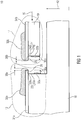
- Fig. 1 shows a schematic cross-sectional view of a MEMS switch 10.
- the MEMS switch 10 comprises a first contact arrangement 12 and a second contact arrangement 14, the contact arrangements 12 and 14 being movable with respect to each other along a moving direction 16 and/or an opposing direction, e.g., in terms of moving back and forth.
- the movement allows for obtaining (closing) and/or opening an mechanic and electric contact between the contact arrangements 12 and 14 and thus for the MEMS switch 10 comprising a closed state or an open state.
- Movement of the contact arrangement(s) may be obtained by actuating one, e.g., the second, contact arrangement 14 with an actuator with respect to the first contact arrangement 12 being arranged statically.
- the actuator may be, for example, an electrostatic, an electrodynamic, a piezoelectric actuator or the like.
- the first contact arrangement 12 may be movable with respect to the second contact arrangement 14. Simplified, the first contact arrangement 12 may be arranged at or be a part of a substrate 18 of the MEMS switch 10.
- the second contact arrangement 14 may be moved with respect to the first contact arrangement 12, for example, by a contact plunger of an actuator.
- the first and the second contact arrangements 12 and 14 each comprise a side (side wall) 22, 24, respectively.
- Each side 22 and 24 comprises a recessed portion 22a or 24a and a projected portion 22b or 24b.
- the projected portions 22b and 24b are projected with respect to the respective recessed portion 22a or 24a, preferably at least partially along a direction parallel to the movement direction 16.
- the first contact arrangement 12 comprises a tear-off edge 26 separating the recessed portion 22a from the projected portion 22b of the side 22.
- the second contact arrangement 14 comprises a tear-off edge 28 separating the recessed portion 24a and the projected portion 24b of the side 24.
- a first contact material 32a is arranged at a first signal line 34a, the first signal line 34a forming an overhung 36a with respect to the substrate 18.
- the overhung 36a i.e., a portion of the first signal line 34a laterally extending beyond the substrate 18 along the movement direction 16
- the contact material 32a may be arranged (deposited) at the first signal line 34a and at the projected portion 22b and at the recessed portion 22a.
- Deposition of the first and/or the second contact material 32a and/or 32b may be executed by any appropriate process, for example, an electroforming process, a CVD process or a PVD process.
- the tear-off edge 26 and/or the overhung 36a allow for the contact material 32a arranged at the recessed portion 22a not influencing the switching behavior of the MEMS switch 10.
- the second contact arrangement 14 comprises a second signal line 34b arranged at a substrate 19, for example a movable contact plunger comprising a silicon material.
- the second signal line 34b is configured for providing and/or receiving an electric current or voltage from or to the first signal line 34a when an electric contact is present between the first contact material 32a and a second contact material 32b arranged at the second signal line 34b.
- the second signal line 34b forms an overhung 36b and a corresponding distance between the recessed portion 24 and the projected portion 24b.
- the substrate 19 of the second contact arrangement 14 may comprise same materials when compared to the substrate 18, e.g., when both contact arrangements are formed of a same wafer. Alternatively, both substrates 18 and 19 may be different, e.g., when the second contact arrangement 14 and the first contact arrangement 12 are manufactured separated from each other and combined after manufacturing.
- the first contact material 32a forms an (second) overhung 38a with respect to the first signal line 34a. and thus with respect to the overhung 36a.
- the overhung 38a may be obtained, for example, during deposition of the first contact material 32a.
- the first contact material 32a and/or the second contact material 32b are formed of a conductive material such as a doped semiconductor material (for example, a doped silicon) or a metal material such as gold, silver, copper, platinum, aluminum, ruthenium or the like and/or a combination thereof.
- the first contact material 32a may be different from the second contact material 32b, but is preferably equal to obtain symmetric contact behavior between the first and the second contact arrangement 12 and 14.
- the overhung 36a and 36b define an overhung distance from the respective recessed portion 22a or 24a to the projected portion 22b, 24b, respectively.
- the overhung distance is at least 2 %, at least 5 % or at least 10% of a thickness of the contact material 32a or 32b along a thickness direction 42.
- the thickness direction 42 may be regarded as a height or thickness of the MEMS switch 10 and/or as a dimension of the MEMS switch 10 along a direction along which different layers of the stack (substrate, signal line, contact material, etc.) are arranged.
- the overhung distance defined by the overhung 36a or 36b may be at least 50%, at least 70% or at least 100% of the thickness of the first or second contact material 32a or 32b.
- the overhung distance may be dependent from a type of process for depositing the contact material 32a and/or 32b. In case, the process leads to a low deposition of the contact material 32a and/or 32b at the side 22 or 24 along the movement direction, a lower overhung distance may be sufficient when compared to a process leading to a high deposition of the contact material 32a and/or 32b at the side 22 or 24.
- An extension of the overhung 38a and/or 38b along the movement direction 16 may be different from each other, but is preferably equal within a tolerance range of 100%, 50% or 10% of one of both extensions of the overhung 38a or 38b.
- the contact materials 32a and 32b may be arranged such that the contact materials 32a and 32b comprise a (convex) curvature along the thickness direction 42, leading to a small area or nearly a point of the contact material 32a and 32b having a minimum distance to each other and allowing for low influences of a roughness of the contact material 32a and 32b at a surface thereof and when contacting each other.
- the contact materials 32a and 32b allow for defined contact surfaces, e.g., comprising a low roughness and a defined shape. This allows for a defined distance between the contact arrangements 12 and 14 in an open state of the MEMS switch 10. The defined distance allows for defined (known) forces that are applied to the contact arrangements. The forces and distances may be relevant parameters with respect to a switching speed and/or to contact resistance of the switch.
- the MEMS 10 comprises the tear-off edges 26 and 28 are implemented at both, the first and the second contact arrangement 12 and 14, an arrangement of the tear-off edge 26 or 28, of the overhung 36a and 36b, or of the overhung 38a or 38b at only one of the contact arrangements 12 or 14 may be sufficient to obtain these effects, for example, when the recessed portion of the side of a contact arrangement is recessed with a distance such far that a probably not recessed portion of the other contact arrangement from providing mechanic and/or electric contact to the recessed portion.
- the MEMS switch 10 may be obtained, for example, by a manufacturing process comprising etching of a silicon substrate and arranging different layers at the substrate. This allows for a high accuracy and avoids a subsequent arrangement of further parts.
- the MEMS 10 is described as the signal lines 34a and 34b being arranged at the respective substrate 18 or 19, in addition, between one or both substrates 18 and/or 19 and the respective signal line 34a and/or 34b an insulating layer may be arranged.
- the insulating layer and/or the signal line may then define the overhung 36a and 36b solely or in combination. Arranging an insulating layer may be advantageous in case the substrate 18 and/or 19 comprise conductive materials, wherein the arrangement of the insulating layer may not be necessary, in case the substrate 18 and/or 19 are formed insulating themselves.
- Fig. 2 shows a schematic perspective view of a modified contact arrangement 14' comprising an insulating layer 44 arranged between the substrate 19 and the second signal line 34b.
- the insulating layer 44 may comprise a silicon(di)oxide material and/or other insulating materials.
- the contact material arranged at the recessed portion 24a and the projected portion 24b and the second signal line 34b is not shown.
- a surface of the insulating layer 44 averted from the substrate 19 defines a main surface 46 of the contact arrangement 14'.
- the main surface 46 may be arranged along any direction but is preferably arranged such that a lateral extension of the main surface 46 is at predominantly (i.e., within a tolerance range of 30°, 20° or 10°) along the moving direction 16. This allows for implementing an in-plane principle of the MEMS switch.
- the signal line 34b is arranged at the main surface 46.
- the distance 36b is defined by the overhung 36b of the insulating layer 44 with respect to the substrate 19.
- a surface 45 of the insulating layer 44 that is uncovered by the substrate 19 is indicated as a shaded flat arranged at a side (surface) of the insulating layer 44 opposing the main surface 44, i.e., facing the substrate 19.
- the contact material may be arranged at the main surface 46 and may contact the signal line 34b and the projected portion 24b.
- the contact material may also be arranged at the recessed portion 24a, wherein this portion of the contact material may be excluded from influencing the electric or mechanic contact with another contact arrangement.
- an insulating layer 44 may also be arranged at the first (static) contact arrangement or at another movable contact arrangement.
- Fig. 3a shows a schematic cross-sectional view of a MEMS switch 30 according to an embodiment.
- the MEMS switch 30 comprises a modified first contact arrangement 12' and the modified contact arrangement 14', wherein the modified contact arrangement 12' s modified as described with respect to the modified contact arrangement 14'
- the substrate 19 may be, for example, part of a contact plunger as will be described with respect to Fig. 4 .
- An insulating layer 44b e.g., the insulating layer 44, is arranged at the substrate 19 and defines the overhung 36b.
- the contact materials 32a and 32b are equal and may be, for example, the contact material 32a or 32b, which is arranged at the contact arrangement 14' such that it forms the overhung 38b along the movement direction 16, allowing for contacting the first contact arrangement 12' by the contact material 32 instead of the insulating layer 44b or the signal line 34b.
- the first contact arrangement 12' is formed at the substrate 18.
- a contact carrier 46 is arranged.
- the contact carrier 46 may be, for example, a layer grown at the substrate 18 during manufacturing.
- the contact carrier 46 may comprise a silicon material, a doped silicon material or a silicon oxide, but may also comprise other materials.
- the contact carrier 46 may also comprise materials comprised by the substrate 18 or may be the substrate 18, i.e., the contact carrier 46 may be formed integrally with the substrate 18.
- an insulating layer 44a comprising insulating materials such as a silicon(di)oxide is arranged forming the overhung 36a with respect to the contact carrier 46.
- the first signal line 34a is arranged at the insulating layer 44a, wherein the insulating layer 44a allows an insulation of the first signal line 34a with respect to the contact carrier 46 and/or the substrate 18 and vice versa.
- the contact material 32 is arranged at the insulating layer 44a and the first signal line 34a and forms the overhung 38a with respect to the insulating layer 44a.
- the electric contact between the first and the second contact arrangement 12' and 14' is provided by the respective contact material 32, wherein the equal type of contact material 32 at both contact arrangements 12' and 14' allows for symmetric forces and a simple arrangement during manufacturing as only one material has to be applied at different locations.
- Fig. 3b shows a schematic cross-sectional view of a MEMS switch 30' which comprises a modified arrangement of the signal lines 34a and 34b when being compared to the MEMS switch 30,
- the signal lines 34a and 34b extend to a side of the insulating layer 44a, 44b respectively, the side forming at least partially the projected portion 22a, 24a respectively.
- the projected portion 22a comprises a side of the first signal line 34a being parallel to the side of the insulating layer 44a partially forming the projected portion 22a.
- the projected portion 24a comprises a side of the second signal line 34b being parallel to the side of the insulating layer 44b forming partially the projected portion 24a.
- the overhung 36a may be formed by the insulating layer 44a in combination with the first signal line 34a with respect to the contact carrier 46.
- the overhung 36b may be formed by the insulating layer 44b in combination with the second signal line 34b with respect to the substrate 19.
- the first and/or the second signal line 34a and/or 34b may form an overhung with respect to the insulating layer 44a, 44b respectively.
- the insulating layer 44a and/or 44b may form no overhung with respect to the contact carrier, the substrate 19 respectively, wherein an overhung of the signal line 34a or 34b is formed with respect to the contact carrier 46, the substrate 19 respectively.
- the respective overhung 36a or 36b and the respective tear-off edge may be understood as a total overhung (tear-off edge) of the respective signal line 34a or 34b and/or the insulating layer 44a or 44b with respect to the contact carrier 46, the substrate 19 respectively.
- the projected portion 22a or 24b comprising the insulating layer 44a, 44b respectively and the signal line 34a, 34b respectively allows for a mutual support of the insulating layer and the signal line when receiving forces and/or pressures when the electric and mechanic contact is obtained to the other contact arrangement 12' or 14'. This allows for an increased number of options when selecting a type of the contact material 32a and/or 32b as the contact pressures and forces are not only received by a single layer.
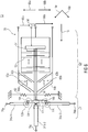
- Fig. 4 shows a schematic block diagram of a MEMS switch 40 comprising an electrostatic (micro) actuator 48.
- the MEMS switch 40 is, for example, configured as an in-plane actuated switch, i.e., the movement direction 16 is predominantly perpendicular to the thickness direction of the MEMS stack.
- the electrostatic actuator 48 comprises static electrodes 52 and movable electrodes 54, which are movable with respect to the static electrodes 52 when applying a voltage 56 between the static and the movable electrodes 52 and 54.
- the electrodes 52 and 54 may be arranged, for example, as comb-shaped electrodes but may also comprise a different configuration.
- the electrostatic actuator comprises a push rod 58 connected to the movable electrodes 54 allowing for a movement of the push rod 58 along the movement direction 16 based on an attraction or repulsion of the movable electrodes 54 with respect to the static electrodes 52.
- the electrostatic actuator further comprises a restoring arrangement 62, for example having a spring element or the like for restoring a state obtained when applying no voltage 56 or a voltage 56 according to zero.
- the restoring arrangement 62 may be arranged between a substrate or another fixed section of the MEMS switch 40 and the push rod 58 and be configured for applying a restoring force to the push rod 58.
- applying a voltage 56 may lead to a movement, probably along the movement direction 16 or an opposing direction for opening or closing electric contacts, wherein the restoring arrangement 62 enhances or provides closing or opening the electric content, i.e., obtaining the initial state.
- the restoring arrangement may also be arranged at a contact plunger 64 connected to the push rod 58.
- the contact plunger 64 is arranged, i.e. connected thereto and moved according to the movement of the push rod 58.
- the push rod may be formed as a rod or a flat or the like and may comprise a surface arranged towards the (static) contact arrangements 12a and 12b to be connected.
- the contact arrangements 14a and 14b are arranged opposing the contact arrangements 12a, 12b respectively.
- Two movable contact arrangements 14a and 14b are arranged at the contact plunger 64.
- the movable contact arrangements 14a and 14b are electrically interconnected, for example, by the second signal line 34b.
- the contact plunger 64 may provide or be the substrate 19 depicted in Fig. 1 .
- the MEMS switch 40 further comprises two static contact arrangements 12a and 12b.
- the MEMS switch 40 is configured for providing a mechanic and electric contact between the contact arrangements 12a and 14a and between the contact arrangements 12b and 14b in a first state (closed contact).
- the contact arrangements 12a and 12b are electrically interconnected by the electric contact to the contact arrangements 14a and 14b and a first segment 34a-1 and a second segment 34a-2 of the first signal line 34a are electrically interconnected, i.e., the MEMS switch 40 is closed.
- the MEMS switch 40 shows a single pole single throw (SPST) switch allowing for closing and interrupting (opening) the signal line 34a by electrically connecting or separating segments 34a-1 and 34a-2 thereof.
- a further signal line 66 for example, a reference signal or ground line or ground plate may be arranged.
- the further signal line 66 and the signal line 34a may form a (switched) wiring system, e.g., supplying a switched device.
- the configuration shown allows for separating the MEMS switch 40 into an actuator part 68 and a radio frequency (RF) signal part 72.
- the actuator part 68 and the RF signal part 72 are separated from each other by the push rod 58, i.e., the push rod 58 may be used for mechanically linking both parts 68 and 72 and for transferring the actuation force to the contact mechanism.
- the MEMS switch 40 is shown having two movable contact arrangements 14a and 14b, arranged at the contact plunger 64, also one, three or more contact arrangements 14 and/or 14' may be arranged.
- one of the segments 34a-1 or 34-2 may comprises a constant contact with the push rod 58 and with a single contact arrangement 14 wherein the push rod is configured for mechanically and electrically connecting to a single contact arrangement 12.
- movement direction 16 is depicted as a straight (linear) direction, the movement direction 16 may also comprise a curved pathway.
- the push rod 58 may be configured for providing a wiping movement, e.g., when one end is hinged to a fixed section and a free end is configured for opening and closing the electric contact.
- the MEMS switch 40 comprises the contact arrangements 12a and 12b, one or both of them may be formed as a modified contact arrangement as described with respect to Fig. 2 .
- the MEMS switch 40 may comprise a different number of contact arrangements 12 and/or 12'.
- Fig. 4 shows an electrostatically actuated micro-mechanical switching device with movable elements for making and breaking at least one Ohmic contact by motion predominantly in the plane of a first substrate surface.
- the MEMS switch 40 comprises a micro actuator 48 with comb-shaped interacting fixed electrodes 52 and movable electrodes 54, the push rod 58 being mechanically connected with the movable electrodes 54 and extending through the area of the electrodes.
- the micro-actuator 48 comprises the movable contact plunger 64 comprising at least one movable contact element (contact arrangement) 14a and/or 14b and at least one restoring spring 62 being mechanically connected with the push rod 58 or with the movable contact plunger 64.
- At least one fixed contact arrangement is configured for interacting with the at least one movable contact arrangement for making and breaking an electric contact.
- the MEMS switch 40 further comprises a wiring system, which is electrically connected to at least one of the fixed contact arrangements, and which comprises at least one electric signal line.
- At least one of the contact arrangements is formed on a layer of insulating material that is part of the contact plunger 64 or that is part of the fixed contact carrier 46 and is freestanding for a certain dimension (overhung 36a and/or 36b) that is large enough to exclude the surface of the contact material of the side wall (recessed portion) of the contact plunger 64, and of the fixed contact carrier 46 from contact forming.
- the segments 34a-1 and 34a-2 and the further signal line 66 form a signal path that is configured for being switched on or off by the MEMS switch 40.
- Fig. 5 shows a schematic block diagram of a MEMS switch 50 being modified when compared to the MEMS switch 40.
- the MEMS switch 50 comprises a modified RF signal part 72' and comprises three movable contact arrangements 14a-c arranged at the contact plunger 64, wherein the movable contact arrangements 14a and 14b are arranged at an external section of the contact plunger 64, wherein the movable contact arrangement 14c is arranged at a central (inner) area of the contact plunger 64, i.e., of the surface thereof.
- the movable contact arrangements 14a-c are electrically interconnected.
- the MEMS switch 50 comprises three static contact arrangements 12a-c arranged opposing the movable contact arrangements 14a-c, wherein the contact arrangements 12a and 14a are associated to each other, wherein the contact arrangements 12b and 14b are associated to each other and wherein the contact arrangements 12c and 14c are associated to each other.
- the contact arrangements 12a-c and 14a-c and the contact arrangements 12b and 14b form an electric contact such that the segments 34a-1 and 34a-2 are electrically interconnected.
- the initial state may be obtained for example as a first actuated state that is, when being compared to an unactuated state (e.g., voltage 56 of approximately zero), obtained when applying the voltage 56 at a first level, such that the push rod 58 and the contact plunger 64 are moved towards the contact arrangements 12a-c and to allow for the mechanical contact between the arrangements 12a/14a and 12b/14b.
- an unactuated state e.g., voltage 56 of approximately zero
- the initial state may be obtained by moving, e.g., biasing, the push rod 58 and the contact plunger 62 into a position in which the electric contact between the contact arrangements 12a-/14a and 12b/14b is obtained.
- This position may be locked or fixed in terms that in case no voltage 56 is applied, the position may be maintained while switching to another contact scenario when applying the voltage 56.
- the contact plunger 64 is elastic and configured for bending when applying a mechanic force thereto. In an actuated state, the push rod 58 and therefore the contact plunger 64 are moved along the movement direction 16, for example when the voltage 56 is increased or reduced resulting in a bending of the contact plunger 64.
- the static contact arrangement 12c and the movable contact arrangement 14c are configured for providing an electric contact in the second state.
- a first mechanic contact arrangement 74a is arranged fixed or static with respect to the contact plunger 64.
- a second mechanic contact arrangement 74b is arranged at the contact plunger 64 between the movable contact arrangements 14c and 14b opposing the first mechanic contact arrangement 74a.
- a distance between the mechanic contact arrangements 74a and 74b may be lower when compared to a distance between the contact arrangements 12c and 14c in the initial state such that, when switching from the initial state to the actuated state, the mechanic contact between the mechanic contact arrangement 74a and 74b is provided applying a force to the contact plunger 64 leading to an opening of the electric contact between the contact arrangements 12b and 14b while maintaining the electric contact between the contact arrangements 12a and 14a.
- the electric contact between the contact arrangements 12c and 14c is provided such that the segment 34a-1 is connected to a segment 34a-3 of the signal line.
- the mechanic contact arrangements 74a and 74b may comprise any appropriate shape and/or materials.
- the mechanic contact arrangements 74a and/or 74b may be formed according to the contact arrangements 12a-c, 14a-c, respectively, probably without electrically connecting one or both of the contact arrangements 74a and 74b to a signal path.
- a common signal port 76a connected to the segment 34a-1 may be connected to a first switched signal port 76b connected to the segment 34a-2 in the initial state and to a second switched signal port 76c connected to the segment 34-3 in the actuated state while opening the first signal path.
- This may also be called a single pole double throw (SPDT) configuration and/or a SPDT lift-configuration as the movable contact arrangement 14b is lifted with respect to the static contact arrangement 12b when switching from the initial state to the actuated state.
- the contact arrangements 12a and 14a may be referred to as a permanently switched contact pair.
- the contact arrangements 12b and 14b may be referred to as a normally (in the initial state) closed contact pair.
- the contact arrangements 12c and 14c may be referred to as a normally opened contact pair, wherein normally open and normally closed may be read in term of an unactuated micro actuator 48.
- the terms normally opened and normally closed may be exchanged in case the initial state is obtained when actuating the micro actuator 48.
- the MEMS switch 50 comprises signal lines 34a-1, 34a-2 and 34a-3, the movable contact elements 14a-c, the fixed contact elements 12a-c and the movable contact plunger 64.
- the mentioned elements are building one of two possible signal paths depending on the actuation state of the switch that way that the movable contact plunger 64 is elastic and contains four movable contact elements 12-c and 47b opposite to fixed contact elements 12a-c and 74a building the permanently closed electric contact pair 12a/14a.
- the normally closed electric contact pair 12b/14b, the normally opened electric contact pair 12c/14c and the normally opened mechanical contact pair 74a-74b build a mechanical stopper.
- the permanently closed electric contact pair 12a-14a and the normally closed electric contact pair 12b/14b establish the (first) signal path between the common signal port 76a and the first switched signal port 76b.
- the permanently closed electric contact pair 12a/14a and the normally opened electric contact pair 12c/14c establish the signal path between the common signal port 76a and the second switched signal port 76c.
- the mechanic contact arrangements 74a and 74b may also be configured for performing an electric contact according to the contact arrangements 12a-c and 14a-c, i.e., a further signal line may be arranged at the contact arrangement 74a.
- Fig. 6 shows a schematic block diagram of a MEMS switch 60 comprising a modified actuator part 68' and a modified RF signal part 72" when compared to the MEMS switch 40 and the MEMS switch 50.
- the MEMS switch 60 comprises a micro actuator 78 which is extended (modified) when compared to the micro actuator 48.
- the micro actuator 78 comprises the micro actuator 48 and comprises additional oblique fixed electrodes 82a and 82b and oblique movable electrodes 84a and 84b, wherein the oblique movable electrodes 84a and 84b are mechanically connected or linked to the push rod 58.
- the oblique electrodes 82a and 84a may be arranged, for example, comb-shaped, and/or comparable to the electrodes 52 and 54 and form port selecting electrodes 85a for selecting a first port to be connected (port 1 selecting electrodes).
- the oblique electrodes 82b and 84b may be arranged, for example, comb-shaped, and/or comparable to the electrodes 52 and 54 and form port selecting electrodes 85b for selecting a second port to be connected (port 2 selecting electrodes). Simplified a two-dimensional movement of the contact plunger 64 is enabled.
- a voltage 86a or 86b between the oblique electrodes 82a and 84a (actuation of the port 1 selecting electrodes 85a), between the oblique electrodes 82b and 84b (actuation of the second port), respectively, allows for a displacement of the push rod and thus for a displacement of the contact plunger 64 along a lateral direction 88a or 88b oriented essentially perpendicular to the moving direction 16.
- the moving direction is referred to as a forward direction
- the lateral directions 88a and 88b may be referred to as left and right or up and down.
- the oblique movement directions 16a and 16b of the contact plunger 64 comprising an angle of larger than zero with respect to the movement direction 16, preferably between 0° and 90°, between 10° and 80° or between 20° and 70°.
- the oblique electrodes 82a, 82b, 84a and 84b are arranged obliquely with respect to the moving direction 16.
- the movable contact arrangements 14a and 14b are arranged at the external or outer regions of the contact plunger 64 with respect to an inner portion thereof, wherein the movable contact arrangement 14c is arranged at the inner portion of the contact plunger.
- the MEMS switch 60 comprises the fixed contact arrangements 12a-c arranged opposing the moveable contact arrangements 14a-c along the movement direction 16 and in an unactuated state of the MEMS switch 60.
- One or more of the contact arrangements 12a-c and/or 14a-c may also be arranged obliquely with respect to the movement direction 16, for example to enable a parallel or almost parallel arrangement of the sides of two contact arrangements brought into contact with each other, when contacting to each other.
- the contact arrangements may also be arranged as such that the sides comprise an oblique angle with respect to each other.
- the MEMS switch 60 is configured for providing a movement of the push rod 58 along the directions 88a and/or 16a such that an electric contact between the contact arrangements 12a and 14a and between the contact arrangements 12c and 14c is obtained. This allows for electrically interconnecting the segments 34a-1 and 34a-3 and thus the signal ports 76a and 76c which form a first pair of signal ports.
- the contact arrangements 12c and 14c may remain unconnected to each other in the first actuation state.
- the MEMS switch 60 In a second actuated state of the MEMS switch 60 in which the oblique electrodes 82a and 84a are not providing an electrostatic force (or a low force) with respect to each other and/or in which the oblique electrodes 82b and 84b are attracted with respect to each other, the MEMS switch 60 is configured for providing a movement of the push rod 58 along the directions 88b and/or 16b such that the electric contact between the contact arrangements 12b and 14b and between the contact arrangements 12c and 14c is obtained. This allows for interconnecting the segments 34a-2 and 34a-3, the signal ports 76b and 76c, respectively which form a second pair of signal ports. The contact arrangements 12a and 14a may remain unconnected to each other in the second actuation state.
- the voltages 86a and 86b may be almost equal or zero such that a (straight) movement of the push rod 58 along the movement direction 16 is obtained. This allows for interconnecting the segments 34a-1 and 34a-2, the signal ports 76a and 76b, respectively which form a third pair of signal ports.
- the contact arrangements 12c and 14c may remain unconnected to each other in the third actuation state.
- the voltage 56 may be zero or that low that no contact at the contact plunger is obtained.
- the voltages 86a and 86b may be almost equal or zero such that a movement along the direction 88a or 88b is prevented and such that the segments 34a-1, 34a-2 and 34a-3 are electrically separated with respect to each other.
- the MEMS switch 60 is described as being actuated for moving the movable push rod 58 along one of the movement directions 16, 16 or 16b by applying the voltage 56 or by the voltage 56 in combination with the voltage 86a and/or 86b
- the MEMS 60 may for moving the push rod along the directions 88a or 88b, i.e., to obtain a lateral movement perpendicular to the movement direction 16 with a low voltage 56 or even a voltage 56 of zero. This allows for avoiding the oblique movement 16a and/or 16b.
- the MEMS switch 60 is a switching device comprising the signal lines (segments) 34a-1, 34a-2 and 34a-3, the movable contact elements 14a-c, the fixed contact elements 12a-c and the movable contact plunger 64.
- the mentioned elements are configured for building one of two (or optionally three) possible signal paths depending on the actuation state of the switch 60 that way that the push rod 58 and the movable contact plunger 64 are driven by the micro-actuator 78 consisting of fixed electrode fingers 52, 82a and 84b and of movable electrode fingers 54, 84a and 84b.
- the electrode fingers are arranged in the electrode field (of the actuator 48) for switch closing motion (switching first pair of signal ports) by the voltage 56, in an electrode field for the port 1 selecting electrodes 85a to be selected (selection motion) by applying the voltage 86a and in an electrode field of the port 2 selecting electrodes 85b to be selected (selection motion) by applying the voltage 86b.
- the MEMS switch is configured for either closing the common electric contact pair by contacting the static contact arrangement 12c with the movable contact plunger, i.e., with the movable contact arrangement 14a or 14b, and to contact the moveable contact plunger to the signal port 76a to enable the first pair of signal ports in case that an actuation voltage is applied to the electrode field (electrodes 82a/84a).
- the MEMS switch is further configured for actuating the electrode field for port selection motion (voltage 56).
- the MEMS switch 60 is configured for closing the common electric contact pair, i.e. to provide the electric contact between the contact arrangements 12a and 14a and between the contact arrangements 12b and 14c while not connecting the contact arrangements 12c and 14c, for example, by only applying the voltage 56 while not applying the voltages 86a and 86b or by applying equal voltages 86a and 86b to obtain a movement of the contact plunger 64 along the movement direction 16.
- MEMS switches are described as having exclusively contact arrangements according to one or more embodiments, there may also be embodiments comprising a hybrid form in which only some of the electric contacts are formed as described above.
- the above described embodiments provide switching devices with a defined contact surface and defined open contact distance that is less influenced by roughness and varying thickness in the configuration of an SPST switch or in the configuration of a SPDT switch with one movable contact part that connects both signal ports of an SPST switch or the common signal port either to the first or to the second signal port in case of an SPDT switch.
- the described concept combines relatively strong forces for making and breaking the metal contacts consisting of movable contact elements (contact arrangements) and fixed contact elements (contact arrangements) with relatively low actuation voltage and may be fabricated by MEMS technologies. Low voltage operation may lead to a necessity to apply an in-plane actuation principle with large electrode areas and to spatially separate the RF signal part from the micro actuator. Above-described embodiments provide a solution for such a necessity.
- MEMS switches 40, 50 and 60 have been described as comprising the contact arrangements 12 and 14, some or all of the contact arrangements may also be formed as a modified version thereof described with respect to Fig. 2 .
- MEMS switches having more than three fixed contact arrangements or more than three movable contact arrangements.
- the MEMS switches may be driven by actuators comprising two, three or more states to obtain any switching behavior.
- MEMS switches have been described as switching a signal line from one static contact arrangement to another, wherein the movable contact arrangements are electrically interconnected, also the static contact arrangements may be electrically interconnected, wherein a signal path to be switched or implemented may be defined by signal lines of the movable contact arrangements not or only partially electrically interconnected.
- aspects have been described in the context of an apparatus, it is clear that these aspects also represent a description of the corresponding method, where a block or device corresponds to a method step or a feature of a method step. Analogously, aspects described in the context of a method step also represent a description of a corresponding block or item or feature of a corresponding apparatus.
Landscapes
- Physics & Mathematics (AREA)
- Electromagnetism (AREA)
- Micromachines (AREA)
Description
- The present invention is related to a microelectromechanical switch and a method for manufacturing the same. The present invention is further related to a device for controlled distribution of radio frequency (RF) signals and in particular small size switching devices for broadband signals in a single pole single throw (SPST) and in a single pole double throw (SPDT) configuration with metal contacts.
- Known switches according to prior art will be described in the following while making reference to
Fig. 7 showing a schematic typical cross section view of the layer thickness.Contact surfaces contact elements movable contact element 106 and of thefixed contact element 108 and they are connected to thesignal lines contact surfaces signal lines contact elements movable contact element 106 and of thefixed contact element 108 and may be connected tosignal lines - The precision of the contact geometry needs to be high in order to control the contact forces and to define the gap between the contacts in an open state of the switch. From electroforming and CVD it is known that the side wall surfaces are coated by the metal with a similar thickness in comparison to the top surface of the
contact elements contact material - MEMS switch according to
EP 2 365 499 A1 - MEMS switches according to
DE 10 2007 035 633 B4 - A MEMS switch according to the characterising portion of
claim 1 and a method for manufacturing a MEMS switch according to the characterising portion of claim 15 is known fromUS 2004/0216988 A1 . - Thus, there exists a need for enhanced microelectromechanical switches.
- An object of the present invention, therefore, is to provide a microelectromechanical switch and a method for manufacturing the same, the microelectromechanical switch comprising a precise switching behavior when switching the electric contact.
- This object is achieved by a microelectromechanical switch in accordance with
claim 1 and a method for manufacturing the same in accordance with claim 15. - The present invention is based on the finding that an enhanced microelectromechanical (MEM) switch forming a microelectromechanical system (MEMS), comprising contact surfaces with a low roughness and a defined distance between the contact elements in an open-state of the switch may be obtained by implementing a tear-off edge at a first or a second contact arrangement for providing the electric contact. The tear-off edge allows for interrupting and/or reducing a deposition of contact materials at surfaces recessed by the tear-off edge with respect to projected surfaces such that a surface area influencing the contact behavior may be reduced when compared to known concepts and/or may be arranged with low tolerances such as a low roughness of the contact material. A small area in which the contact may occur allows for a low deviations between switches. Defined material extensions (thickness and/or roughness) of the contact material at the side comprising the tear-off edge allows for a defined and precise switching behavior of the switch.
- An embodiment of the present invention provides a MEMS switch comprising a first and a second contact arrangement having a side facing each other. The first and the second contact arrangement are movable with respect to each other and configured for providing an electric contact in a first state and for not providing the electric contact in a second state. A first contact material is arranged at the side of the first contact arrangement. A second contact material is arranged at the side of the second contact arrangement. The side of the first and the side of the second contact arrangement comprise a recessed region and a projected region projected with respect to the recessed region. The projected region and the recessed region are separated from each other by a tear-off edge, wherein the first and the second contact material are arranged at the recessed region and the projected region of the respective side. The electric contact is provided between the first and the second contact material in the projected region of the sides and not provided in the recessed region in the first state. This allows for avoiding influences of the contact materials to the electric contact and/or the switching behavior of the switch in the recessed region and for a defined switching behavior of the switch in the projected region.
- A further embodiment provides a MEMS switch comprising the contact materials having a curved surface such that an area in which the electric contact is provided is low such that a highly defined switching behavior is obtained. A further embodiment of the present invention provides a method for manufacturing a MEMS switch. The method comprises an arrangement of a first and a second contact arrangement such that a side of the first and of the second contact arrangement face each other such that the first and the second contact arrangement are movable with respect to each other and provide an electric contact in a first state and do not provide the electric contact in a second state. The method further comprises an arrangement of a first contact material at the side of the first contact arrangement and an arrangement of a second contact material at the side of the second contact arrangement. The side of the first and the side of the second contact arrangement comprise a recessed region and a projected region projected with respect to the recessed region, the projected region and the recessed region separated from each other by a tear-off edge. The first and the second contact material are arranged at the recessed region and at the projected region of the respective side. The electric contact is provided between the first and the second contact material in the projected region of the sides and not provided in the recessed region in the first state.
- Further embodiments are the subject matter of the dependent claims.
- Subsequently, preferred embodiments of the present invention are described with respect to the accompanying drawings, in which:
- Fig. 1
- shows a schematic cross-sectional view of a MEMS switch according to an embodiment;
- Fig. 2
- shows a schematic perspective view of a modified contact arrangement modified with respect to
Fig. 1 and comprising an insulating layer forming a tear-off edge according to an embodiment; - Fig. 3a
- shows a schematic cross-sectional view of a MEMS switch comprising two contact arrangements having insulating layers each forming a tear-off edge forming according to an embodiment;
- Fig. 3b
- shows a schematic cross-sectional view of a MEMS switch which comprises a modified arrangement of signal lines when being compared to the MEMS switch shown in
Fig. 3a ; - Fig. 4
- shows a schematic block diagram of a MEMS switch comprising a single pole single throw configuration according to an embodiment;
- Fig. 5
- shows a schematic block diagram of a MEMS switch comprising a single pole double throw configuration according to an embodiment;
- Fig. 6
- shows a schematic block diagram of a MEMS switch comprising a modified actuator part for enabling a two-dimensional movement of a contact plunger according to an embodiment; and
- Fig. 7
- shows a schematic cross-sectional view of a MEMS switch according to prior art.
- Equal or equivalent elements or elements with equal or equivalent functionality are denoted in the following description by equal or equivalent reference numerals even if occurring in different figures.
- In the following description, a plurality of details is set forth to provide a more thorough explanation of embodiments of the present invention. However, it will be apparent to those skilled in the art that embodiments of the present invention may be practiced without these specific details. In other instances, well known structures and devices are shown in block diagram form rather than in detail in order to avoid obscuring embodiments of the present invention. In addition, features of the different embodiments described hereinafter may be combined with each other, unless specifically noted otherwise.
- In the following, reference will be made to microelectromechanical (MEMS) switches which are actuated (electro-)mechanically. For providing the mechanical actuation, an actuator may be arranged such that a microelectromechanical system (MEMS) switch is obtained.
-
Fig. 1 shows a schematic cross-sectional view of aMEMS switch 10. TheMEMS switch 10 comprises afirst contact arrangement 12 and asecond contact arrangement 14, thecontact arrangements direction 16 and/or an opposing direction, e.g., in terms of moving back and forth. The movement allows for obtaining (closing) and/or opening an mechanic and electric contact between thecontact arrangements MEMS switch 10 comprising a closed state or an open state. - Movement of the contact arrangement(s) may be obtained by actuating one, e.g., the second,
contact arrangement 14 with an actuator with respect to thefirst contact arrangement 12 being arranged statically. The actuator may be, for example, an electrostatic, an electrodynamic, a piezoelectric actuator or the like. Alternatively or in addition, thefirst contact arrangement 12 may be movable with respect to thesecond contact arrangement 14. Simplified, thefirst contact arrangement 12 may be arranged at or be a part of asubstrate 18 of theMEMS switch 10. Thesecond contact arrangement 14 may be moved with respect to thefirst contact arrangement 12, for example, by a contact plunger of an actuator. - The first and the
second contact arrangements side portion portion portions portion movement direction 16. - The
first contact arrangement 12 comprises a tear-off edge 26 separating the recessedportion 22a from the projectedportion 22b of theside 22. Thesecond contact arrangement 14 comprises a tear-off edge 28 separating the recessedportion 24a and the projectedportion 24b of theside 24. Afirst contact material 32a is arranged at afirst signal line 34a, thefirst signal line 34a forming an overhung 36a with respect to thesubstrate 18. The overhung 36a (i.e., a portion of thefirst signal line 34a laterally extending beyond thesubstrate 18 along the movement direction 16) forms a corresponding distance between the recessedportion 22a and the projectedportion 22b of theside 22 along a direction along which thesignal line 34a extends beyond thesubstrate 18. During the deposition of thecontact material 32a thecontact material 32a may be arranged (deposited) at thefirst signal line 34a and at the projectedportion 22b and at the recessedportion 22a. Deposition of the first and/or thesecond contact material 32a and/or 32b may be executed by any appropriate process, for example, an electroforming process, a CVD process or a PVD process. The tear-off edge 26 and/or the overhung 36a allow for thecontact material 32a arranged at the recessedportion 22a not influencing the switching behavior of theMEMS switch 10. - The
second contact arrangement 14 comprises asecond signal line 34b arranged at asubstrate 19, for example a movable contact plunger comprising a silicon material. Thesecond signal line 34b is configured for providing and/or receiving an electric current or voltage from or to thefirst signal line 34a when an electric contact is present between thefirst contact material 32a and asecond contact material 32b arranged at thesecond signal line 34b. Thesecond signal line 34b forms an overhung 36b and a corresponding distance between the recessedportion 24 and the projectedportion 24b. Thesubstrate 19 of thesecond contact arrangement 14 may comprise same materials when compared to thesubstrate 18, e.g., when both contact arrangements are formed of a same wafer. Alternatively, bothsubstrates second contact arrangement 14 and thefirst contact arrangement 12 are manufactured separated from each other and combined after manufacturing. - The
first contact material 32a forms an (second) overhung 38a with respect to the first signal line 34a. and thus with respect to the overhung 36a. The overhung 38a may be obtained, for example, during deposition of thefirst contact material 32a. Thefirst contact material 32a and/or thesecond contact material 32b are formed of a conductive material such as a doped semiconductor material (for example, a doped silicon) or a metal material such as gold, silver, copper, platinum, aluminum, ruthenium or the like and/or a combination thereof. - The
first contact material 32a may be different from thesecond contact material 32b, but is preferably equal to obtain symmetric contact behavior between the first and thesecond contact arrangement portion portion contact material thickness direction 42. Thethickness direction 42 may be regarded as a height or thickness of theMEMS switch 10 and/or as a dimension of theMEMS switch 10 along a direction along which different layers of the stack (substrate, signal line, contact material, etc.) are arranged. Alternatively, the overhung distance defined by the overhung 36a or 36b may be at least 50%, at least 70% or at least 100% of the thickness of the first orsecond contact material contact material 32a and/or 32b. In case, the process leads to a low deposition of thecontact material 32a and/or 32b at theside contact material 32a and/or 32b at theside - An extension of the overhung 38a and/or 38b along the
movement direction 16 may be different from each other, but is preferably equal within a tolerance range of 100%, 50% or 10% of one of both extensions of the overhung 38a or 38b. - Based on the overhung 36a, 36b, 38a and 38b, the
contact materials contact materials thickness direction 42, leading to a small area or nearly a point of thecontact material contact material - The
contact materials contact arrangements MEMS switch 10. The defined distance allows for defined (known) forces that are applied to the contact arrangements. The forces and distances may be relevant parameters with respect to a switching speed and/or to contact resistance of the switch. - Although the
MEMS 10 comprises the tear-offedges second contact arrangement off edge contact arrangements - The
MEMS switch 10 may be obtained, for example, by a manufacturing process comprising etching of a silicon substrate and arranging different layers at the substrate. This allows for a high accuracy and avoids a subsequent arrangement of further parts. - Although the
MEMS 10 is described as thesignal lines respective substrate substrates 18 and/or 19 and therespective signal line 34a and/or 34b an insulating layer may be arranged. The insulating layer and/or the signal line may then define the overhung 36a and 36b solely or in combination. Arranging an insulating layer may be advantageous in case thesubstrate 18 and/or 19 comprise conductive materials, wherein the arrangement of the insulating layer may not be necessary, in case thesubstrate 18 and/or 19 are formed insulating themselves. -
Fig. 2 shows a schematic perspective view of a modified contact arrangement 14' comprising an insulatinglayer 44 arranged between thesubstrate 19 and thesecond signal line 34b. The insulatinglayer 44 may comprise a silicon(di)oxide material and/or other insulating materials. The contact material arranged at the recessedportion 24a and the projectedportion 24b and thesecond signal line 34b is not shown. A surface of the insulatinglayer 44 averted from thesubstrate 19 defines amain surface 46 of the contact arrangement 14'. Themain surface 46 may be arranged along any direction but is preferably arranged such that a lateral extension of themain surface 46 is at predominantly (i.e., within a tolerance range of 30°, 20° or 10°) along the movingdirection 16. This allows for implementing an in-plane principle of the MEMS switch. - The
signal line 34b is arranged at themain surface 46. Thedistance 36b is defined by the overhung 36b of the insulatinglayer 44 with respect to thesubstrate 19. Asurface 45 of the insulatinglayer 44 that is uncovered by thesubstrate 19 is indicated as a shaded flat arranged at a side (surface) of the insulatinglayer 44 opposing themain surface 44, i.e., facing thesubstrate 19. The contact material may be arranged at themain surface 46 and may contact thesignal line 34b and the projectedportion 24b. The contact material may also be arranged at the recessedportion 24a, wherein this portion of the contact material may be excluded from influencing the electric or mechanic contact with another contact arrangement. - Although the arrangement of the insulating
layer 44 is described with respect to the second contact arrangement 14', alternatively or in addition, an insulating layer may also be arranged at the first (static) contact arrangement or at another movable contact arrangement. -
Fig. 3a shows a schematic cross-sectional view of aMEMS switch 30 according to an embodiment. When compared to theMEMS switch 10, theMEMS switch 30 comprises a modified first contact arrangement 12' and the modified contact arrangement 14', wherein the modified contact arrangement 12' s modified as described with respect to the modified contact arrangement 14' - The
substrate 19 may be, for example, part of a contact plunger as will be described with respect toFig. 4 . An insulatinglayer 44b, e.g., the insulatinglayer 44, is arranged at thesubstrate 19 and defines the overhung 36b. When compared toFig. 2 , thecontact materials contact material movement direction 16, allowing for contacting the first contact arrangement 12' by thecontact material 32 instead of the insulatinglayer 44b or thesignal line 34b. - The first contact arrangement 12' is formed at the
substrate 18. At the substrate 18 acontact carrier 46 is arranged. Thecontact carrier 46 may be, for example, a layer grown at thesubstrate 18 during manufacturing. Thecontact carrier 46 may comprise a silicon material, a doped silicon material or a silicon oxide, but may also comprise other materials. Alternatively, thecontact carrier 46 may also comprise materials comprised by thesubstrate 18 or may be thesubstrate 18, i.e., thecontact carrier 46 may be formed integrally with thesubstrate 18. At thecontact area 46 an insulatinglayer 44a comprising insulating materials such as a silicon(di)oxide is arranged forming the overhung 36a with respect to thecontact carrier 46. - The
first signal line 34a is arranged at the insulatinglayer 44a, wherein the insulatinglayer 44a allows an insulation of thefirst signal line 34a with respect to thecontact carrier 46 and/or thesubstrate 18 and vice versa. Thecontact material 32 is arranged at the insulatinglayer 44a and thefirst signal line 34a and forms the overhung 38a with respect to the insulatinglayer 44a. Thus, the electric contact between the first and the second contact arrangement 12' and 14' is provided by therespective contact material 32, wherein the equal type ofcontact material 32 at both contact arrangements 12' and 14' allows for symmetric forces and a simple arrangement during manufacturing as only one material has to be applied at different locations. -
Fig. 3b shows a schematic cross-sectional view of a MEMS switch 30' which comprises a modified arrangement of thesignal lines MEMS switch 30, Thesignal lines layer portion portion 22a comprises a side of thefirst signal line 34a being parallel to the side of the insulatinglayer 44a partially forming the projectedportion 22a. The projectedportion 24a comprises a side of thesecond signal line 34b being parallel to the side of the insulatinglayer 44b forming partially the projectedportion 24a. The overhung 36a may be formed by the insulatinglayer 44a in combination with thefirst signal line 34a with respect to thecontact carrier 46. The overhung 36b may be formed by the insulatinglayer 44b in combination with thesecond signal line 34b with respect to thesubstrate 19. Alternatively, the first and/or thesecond signal line 34a and/or 34b may form an overhung with respect to the insulatinglayer layer 44a and/or 44b may form no overhung with respect to the contact carrier, thesubstrate 19 respectively, wherein an overhung of thesignal line contact carrier 46, thesubstrate 19 respectively. Therespective overhung respective signal line layer contact carrier 46, thesubstrate 19 respectively. - The projected
portion layer signal line contact material 32a and/or 32b as the contact pressures and forces are not only received by a single layer. -
Fig. 4 shows a schematic block diagram of aMEMS switch 40 comprising an electrostatic (micro)actuator 48. TheMEMS switch 40 is, for example, configured as an in-plane actuated switch, i.e., themovement direction 16 is predominantly perpendicular to the thickness direction of the MEMS stack. Theelectrostatic actuator 48 comprisesstatic electrodes 52 andmovable electrodes 54, which are movable with respect to thestatic electrodes 52 when applying avoltage 56 between the static and themovable electrodes electrodes - The electrostatic actuator comprises a
push rod 58 connected to themovable electrodes 54 allowing for a movement of thepush rod 58 along themovement direction 16 based on an attraction or repulsion of themovable electrodes 54 with respect to thestatic electrodes 52. The electrostatic actuator further comprises a restoringarrangement 62, for example having a spring element or the like for restoring a state obtained when applying novoltage 56 or avoltage 56 according to zero. The restoringarrangement 62 may be arranged between a substrate or another fixed section of theMEMS switch 40 and thepush rod 58 and be configured for applying a restoring force to thepush rod 58. Simplified, applying avoltage 56 may lead to a movement, probably along themovement direction 16 or an opposing direction for opening or closing electric contacts, wherein the restoringarrangement 62 enhances or provides closing or opening the electric content, i.e., obtaining the initial state. The restoring arrangement may also be arranged at acontact plunger 64 connected to thepush rod 58. - At the
push rod 58, thecontact plunger 64 is arranged, i.e. connected thereto and moved according to the movement of thepush rod 58. The push rod may be formed as a rod or a flat or the like and may comprise a surface arranged towards the (static)contact arrangements contact arrangements contact arrangements movable contact arrangements contact plunger 64. Themovable contact arrangements second signal line 34b. Thecontact plunger 64 may provide or be thesubstrate 19 depicted inFig. 1 . - The
MEMS switch 40 further comprises twostatic contact arrangements MEMS switch 40 is configured for providing a mechanic and electric contact between thecontact arrangements contact arrangements contact arrangements contact arrangements first segment 34a-1 and asecond segment 34a-2 of thefirst signal line 34a are electrically interconnected, i.e., theMEMS switch 40 is closed. - Simplified, the
MEMS switch 40 shows a single pole single throw (SPST) switch allowing for closing and interrupting (opening) thesignal line 34a by electrically connecting or separatingsegments 34a-1 and 34a-2 thereof. Afurther signal line 66, for example, a reference signal or ground line or ground plate may be arranged. Thefurther signal line 66 and thesignal line 34a may form a (switched) wiring system, e.g., supplying a switched device. - The configuration shown allows for separating the
MEMS switch 40 into anactuator part 68 and a radio frequency (RF) signalpart 72. Theactuator part 68 and theRF signal part 72 are separated from each other by thepush rod 58, i.e., thepush rod 58 may be used for mechanically linking bothparts - Although the
MEMS switch 40 is shown having twomovable contact arrangements contact plunger 64, also one, three ormore contact arrangements 14 and/or 14' may be arranged. For example, one of thesegments 34a-1 or 34-2 may comprises a constant contact with thepush rod 58 and with asingle contact arrangement 14 wherein the push rod is configured for mechanically and electrically connecting to asingle contact arrangement 12. - Although
movement direction 16 is depicted as a straight (linear) direction, themovement direction 16 may also comprise a curved pathway. For example, thepush rod 58 may be configured for providing a wiping movement, e.g., when one end is hinged to a fixed section and a free end is configured for opening and closing the electric contact. - Although the
MEMS switch 40 comprises thecontact arrangements Fig. 2 . Alternatively or in addition, theMEMS switch 40 may comprise a different number ofcontact arrangements 12 and/or 12'. - In other words,
Fig. 4 shows an electrostatically actuated micro-mechanical switching device with movable elements for making and breaking at least one Ohmic contact by motion predominantly in the plane of a first substrate surface. TheMEMS switch 40 comprises amicro actuator 48 with comb-shaped interacting fixedelectrodes 52 andmovable electrodes 54, thepush rod 58 being mechanically connected with themovable electrodes 54 and extending through the area of the electrodes. The micro-actuator 48 comprises themovable contact plunger 64 comprising at least one movable contact element (contact arrangement) 14a and/or 14b and at least one restoringspring 62 being mechanically connected with thepush rod 58 or with themovable contact plunger 64. At least one fixed contact arrangement is configured for interacting with the at least one movable contact arrangement for making and breaking an electric contact. TheMEMS switch 40 further comprises a wiring system, which is electrically connected to at least one of the fixed contact arrangements, and which comprises at least one electric signal line. - At least one of the contact arrangements is formed on a layer of insulating material that is part of the
contact plunger 64 or that is part of the fixedcontact carrier 46 and is freestanding for a certain dimension (overhung 36a and/or 36b) that is large enough to exclude the surface of the contact material of the side wall (recessed portion) of thecontact plunger 64, and of the fixedcontact carrier 46 from contact forming. Thesegments 34a-1 and 34a-2 and thefurther signal line 66 form a signal path that is configured for being switched on or off by theMEMS switch 40. -
Fig. 5 shows a schematic block diagram of aMEMS switch 50 being modified when compared to theMEMS switch 40. TheMEMS switch 50 comprises a modified RF signal part 72' and comprises threemovable contact arrangements 14a-c arranged at thecontact plunger 64, wherein themovable contact arrangements contact plunger 64, wherein themovable contact arrangement 14c is arranged at a central (inner) area of thecontact plunger 64, i.e., of the surface thereof. Themovable contact arrangements 14a-c are electrically interconnected. TheMEMS switch 50 comprises threestatic contact arrangements 12a-c arranged opposing themovable contact arrangements 14a-c, wherein thecontact arrangements contact arrangements contact arrangements - In an initial state of the
MEMS switch 50 thecontact arrangements 12a-c and 14a-c and thecontact arrangements segments 34a-1 and 34a-2 are electrically interconnected. The initial state may be obtained for example as a first actuated state that is, when being compared to an unactuated state (e.g.,voltage 56 of approximately zero), obtained when applying thevoltage 56 at a first level, such that thepush rod 58 and thecontact plunger 64 are moved towards thecontact arrangements 12a-c and to allow for the mechanical contact between thearrangements 12a/14a and 12b/14b. This allows for obtaining a state of theMEMS switch 50 in which no contact between static andmoveable contact arrangements 12a-c and 14a-c is provided. Alternatively, the initial state may be obtained by moving, e.g., biasing, thepush rod 58 and thecontact plunger 62 into a position in which the electric contact between thecontact arrangements 12a-/14a and 12b/14b is obtained. This position may be locked or fixed in terms that in case novoltage 56 is applied, the position may be maintained while switching to another contact scenario when applying thevoltage 56. - The
contact plunger 64 is elastic and configured for bending when applying a mechanic force thereto. In an actuated state, thepush rod 58 and therefore thecontact plunger 64 are moved along themovement direction 16, for example when thevoltage 56 is increased or reduced resulting in a bending of thecontact plunger 64. Thestatic contact arrangement 12c and themovable contact arrangement 14c are configured for providing an electric contact in the second state. A firstmechanic contact arrangement 74a is arranged fixed or static with respect to thecontact plunger 64. A secondmechanic contact arrangement 74b is arranged at thecontact plunger 64 between themovable contact arrangements mechanic contact arrangement 74a. A distance between themechanic contact arrangements contact arrangements mechanic contact arrangement contact plunger 64 leading to an opening of the electric contact between thecontact arrangements contact arrangements push rod 58 and of thecontact arrangement 14c along themovement direction 16, the electric contact between thecontact arrangements segment 34a-1 is connected to asegment 34a-3 of the signal line. - Thus, in the initial state a signal path between the
segments 34a-1 and 34a-2 is provided and in the actuated state a second signal path between thesegments 34a-1 and 34a-3 is provided. Themechanic contact arrangements mechanic contact arrangements 74a and/or 74b may be formed according to thecontact arrangements 12a-c, 14a-c, respectively, probably without electrically connecting one or both of thecontact arrangements - Simplified, a
common signal port 76a connected to thesegment 34a-1 may be connected to a first switchedsignal port 76b connected to thesegment 34a-2 in the initial state and to a second switchedsignal port 76c connected to the segment 34-3 in the actuated state while opening the first signal path. This may also be called a single pole double throw (SPDT) configuration and/or a SPDT lift-configuration as themovable contact arrangement 14b is lifted with respect to thestatic contact arrangement 12b when switching from the initial state to the actuated state. Thecontact arrangements contact arrangements contact arrangements micro actuator 48. The terms normally opened and normally closed may be exchanged in case the initial state is obtained when actuating themicro actuator 48. - In other words, the
MEMS switch 50 comprisessignal lines 34a-1, 34a-2 and 34a-3, themovable contact elements 14a-c, the fixedcontact elements 12a-c and themovable contact plunger 64. The mentioned elements are building one of two possible signal paths depending on the actuation state of the switch that way that themovable contact plunger 64 is elastic and contains four movable contact elements 12-c and 47b opposite to fixedcontact elements 12a-c and 74a building the permanently closedelectric contact pair 12a/14a. The normally closedelectric contact pair 12b/14b, the normally openedelectric contact pair 12c/14c and the normally openedmechanical contact pair 74a-74b build a mechanical stopper. In the non-actuated state of the micro actuator the permanently closedelectric contact pair 12a-14a and the normally closedelectric contact pair 12b/14b establish the (first) signal path between thecommon signal port 76a and the first switchedsignal port 76b. In the actuated state the permanently closedelectric contact pair 12a/14a and the normally openedelectric contact pair 12c/14c establish the signal path between thecommon signal port 76a and the second switchedsignal port 76c. In the actuated state themovable contact element 14b and the fixedcontact element 12b of the normally closed electric contact pair is mechanically separated to each other by bending thecontact plunger 64 due to the mechanical force originating from themicro actuator 48 and the counter force originating from the normally openedelectric contact pair 12c/14c and the normally openedmechanical contact pair 74a/74b. - Alternatively, the
mechanic contact arrangements contact arrangements 12a-c and 14a-c, i.e., a further signal line may be arranged at thecontact arrangement 74a. -
Fig. 6 shows a schematic block diagram of a MEMS switch 60 comprising a modified actuator part 68' and a modifiedRF signal part 72" when compared to theMEMS switch 40 and theMEMS switch 50. The MEMS switch 60 comprises amicro actuator 78 which is extended (modified) when compared to themicro actuator 48. Themicro actuator 78 comprises themicro actuator 48 and comprises additional oblique fixedelectrodes movable electrodes movable electrodes push rod 58. Theoblique electrodes electrodes port selecting electrodes 85a for selecting a first port to be connected (port 1 selecting electrodes). Theoblique electrodes electrodes port selecting electrodes 85b for selecting a second port to be connected (port 2 selecting electrodes). Simplified a two-dimensional movement of thecontact plunger 64 is enabled. - A
voltage oblique electrodes port 1 selectingelectrodes 85a), between theoblique electrodes contact plunger 64 along alateral direction direction 16. When, for example and without limitation, the moving direction is referred to as a forward direction, thelateral directions voltage 56 and of the voltage 68a or 68b effectiveoblique movement directions contact plunger 64 may be obtained, theoblique movement directions movement direction 16, preferably between 0° and 90°, between 10° and 80° or between 20° and 70°. Theoblique electrodes direction 16. - The
movable contact arrangements contact plunger 64 with respect to an inner portion thereof, wherein themovable contact arrangement 14c is arranged at the inner portion of the contact plunger. The MEMS switch 60 comprises the fixedcontact arrangements 12a-c arranged opposing themoveable contact arrangements 14a-c along themovement direction 16 and in an unactuated state of the MEMS switch 60. - One or more of the
contact arrangements 12a-c and/or 14a-c may also be arranged obliquely with respect to themovement direction 16, for example to enable a parallel or almost parallel arrangement of the sides of two contact arrangements brought into contact with each other, when contacting to each other. Alternatively, the contact arrangements may also be arranged as such that the sides comprise an oblique angle with respect to each other. - In a first actuated state, in which the
oblique electrodes oblique electrodes push rod 58 along thedirections 88a and/or 16a such that an electric contact between thecontact arrangements contact arrangements segments 34a-1 and 34a-3 and thus thesignal ports contact arrangements - In a second actuated state of the MEMS switch 60 in which the
oblique electrodes oblique electrodes push rod 58 along thedirections 88b and/or 16b such that the electric contact between thecontact arrangements contact arrangements segments 34a-2 and 34a-3, thesignal ports contact arrangements - In an optional third actuated state of the MEMS switch 60, the
voltages push rod 58 along themovement direction 16 is obtained. This allows for interconnecting thesegments 34a-1 and 34a-2, thesignal ports contact arrangements - In an unactuated state, for example, the
voltage 56 may be zero or that low that no contact at the contact plunger is obtained. Alternatively or in addition thevoltages direction segments 34a-1, 34a-2 and 34a-3 are electrically separated with respect to each other. - This allows for four states to be obtained by the MEMS switch 60, three actuated states and one probably passive state such that the MEMS switch 60 may be referred to as a 4-state SPDT (SPDT 4-state).
- Although the MEMS switch 60 is described as being actuated for moving the
movable push rod 58 along one of themovement directions voltage 56 or by thevoltage 56 in combination with thevoltage 86a and/or 86b, the MEMS 60 may for moving the push rod along thedirections movement direction 16 with alow voltage 56 or even avoltage 56 of zero. This allows for avoiding theoblique movement 16a and/or 16b. - In other words, the MEMS switch 60 is a switching device comprising the signal lines (segments) 34a-1, 34a-2 and 34a-3, the
movable contact elements 14a-c, the fixedcontact elements 12a-c and themovable contact plunger 64. The mentioned elements are configured for building one of two (or optionally three) possible signal paths depending on the actuation state of the switch 60 that way that thepush rod 58 and themovable contact plunger 64 are driven by the micro-actuator 78 consisting of fixedelectrode fingers movable electrode fingers voltage 56, in an electrode field for theport 1 selectingelectrodes 85a to be selected (selection motion) by applying thevoltage 86a and in an electrode field of theport 2 selectingelectrodes 85b to be selected (selection motion) by applying thevoltage 86b. - The MEMS switch is configured for either closing the common electric contact pair by contacting the
static contact arrangement 12c with the movable contact plunger, i.e., with themovable contact arrangement signal port 76a to enable the first pair of signal ports in case that an actuation voltage is applied to the electrode field (electrodes 82a/84a). The MEMS switch is further configured for actuating the electrode field for port selection motion (voltage 56). - In another state the MEMS switch 60 is configured for closing the common electric contact pair, i.e. to provide the electric contact between the
contact arrangements contact arrangements contact arrangements voltage 56 while not applying thevoltages equal voltages contact plunger 64 along themovement direction 16. - Although the above described MEMS switches are described as having exclusively contact arrangements according to one or more embodiments, there may also be embodiments comprising a hybrid form in which only some of the electric contacts are formed as described above.
- The above described embodiments provide switching devices with a defined contact surface and defined open contact distance that is less influenced by roughness and varying thickness in the configuration of an SPST switch or in the configuration of a SPDT switch with one movable contact part that connects both signal ports of an SPST switch or the common signal port either to the first or to the second signal port in case of an SPDT switch.
- The described concept combines relatively strong forces for making and breaking the metal contacts consisting of movable contact elements (contact arrangements) and fixed contact elements (contact arrangements) with relatively low actuation voltage and may be fabricated by MEMS technologies. Low voltage operation may lead to a necessity to apply an in-plane actuation principle with large electrode areas and to spatially separate the RF signal part from the micro actuator. Above-described embodiments provide a solution for such a necessity.
- Although the MEMS switches 40, 50 and 60 have been described as comprising the
contact arrangements Fig. 2 . - Further embodiments provide MEMS switches having more than three fixed contact arrangements or more than three movable contact arrangements. The MEMS switches may be driven by actuators comprising two, three or more states to obtain any switching behavior.
- Although the above described MEMS switches have been described as switching a signal line from one static contact arrangement to another, wherein the movable contact arrangements are electrically interconnected, also the static contact arrangements may be electrically interconnected, wherein a signal path to be switched or implemented may be defined by signal lines of the movable contact arrangements not or only partially electrically interconnected.
- Although some aspects have been described in the context of an apparatus, it is clear that these aspects also represent a description of the corresponding method, where a block or device corresponds to a method step or a feature of a method step. Analogously, aspects described in the context of a method step also represent a description of a corresponding block or item or feature of a corresponding apparatus.
- The above described embodiments are merely illustrative for the principles of the present invention. It is understood that modifications and variations of the arrangements and the details described herein will be apparent to others skilled in the art. It is the intent, therefore, to be limited only by the scope of the impending patent claims and not by the specific details presented by way of description and explanation of the embodiments herein.
Claims (15)
- MEMS (10; 30; 40; 50; 60) switch comprising:a first (12; 12a-c) and a second (14; 14a-c; 14") contact arrangement having a side (22, 24) facing each other, the first (12; 12a-c) and the second contact arrangement (14; 14a-c; 14") movable with respect to each other and configured for providing an electric contact in a first state and for not providing the electric contact in a second state;a first contact material (32; 32a) arranged at the side (22) of the first contact arrangement (12; 12a-c);a second contact material (32; 32b) arranged at the side (24) of the second contact arrangement (14; 14a-c; 14");wherein the side (22) of the first (12; 12a-c) and/or the side (24) of the second contact arrangement (14; 14a-c; 14") comprises a recessed region (22a, 24a) and a projected region (22b, 24b), projected with respect to the recessed region (22a, 24a);wherein the electric contact is provided between the first (32; 32a) and the second contact material (32; 32b) in the projected region (22b, 24b) of the side (22, 24) and not provided in the recessed region (22a, 24a) in the first state,characterised in that the projected region (22b, 24b) and the recessed region (22a, 24a) are separated from each other by a tear-off edge (26, 28), wherein the first (32; 32a) and/or the second contact material (32; 32b) is arranged at the recessed region (22a, 24a) and at the projected region(22b, 24b) of the respective side (22, 24).
- MEMS switch according to claim 1, wherein the tear-off edge (26, 28) of the side (22, 24) of the first (12; 12a-c) or the second contact arrangement (14; 14a-c; 14") defines a first overhung (36a, 36b) of the respective projected portion (22b, 24b) with respect to the respective recessed portion (22a, 24a), wherein the respective contact material (32; 32a, 32b) is arranged such that it forms a second overhung (38a, 38b) with respect to the respective projected portion (22b, 24b).
- MEMS switch according to claim 2, wherein the first (12; 12a-c) or the second contact arrangement (14; 14a-c; 14") comprises a substrate layer (19) and an insulating layer (44a, 44b) arranged at the substrate layer (19), wherein the insulating layer (44a, 44b) forms the first overhung (36a, 36b) and comprises a first surface (24b) that is projected with respect to a surface (24a) of the substrate layer (19) along a moving direction (16) along which the first (12; 12a-c) and the second contact arrangement(14; 14a-c; 14") are movable with respect to each other, wherein a second surface (45) of the insulating layer (44) facing the substrate layer (19) and uncovered from the substrate layer (19) defines the tear-off edge (28).
- MEMS switch according to claim 2 or 3, wherein the first overhung (36a, 36b) defines an overhung distance from the recessed portion (22a, 24a) to the projected portion (22b, 24b), the overhung distance being at least 30 % of a thickness of the first or the second contact material (32; 32a, 32b) along a thickness direction (42) perpendicular to a moving direction (16) along which the first (12; 12a-c) and the second contact arrangement (14; 14a-c; 14") are movable with respect to each other.
- MEMS switch according to one of previous claims, wherein the first contact material (32; 32a) is electrically connected to a first signal line (34a) and wherein the second contact material (32; 32b) is electrically connected to a second signal line (34b), wherein the MEMS switch is configured for electrically connecting the first and the second signal line in the first state.
- MEMS switch according to one of previous claims, wherein the first signal line (34a) or the second signal line (34b) is arranged at a main surface (46) of the first (12; 12a-c) or the second contact arrangement (14; 14a-c; 14"), the main surface (46) being predominantly parallel along a moving direction (16) along which the first (12; 12a-c) and the second contact arrangement (14; 14a-c; 14") are movable with respect to each other, wherein the first (32; 32a) or the second contact material (32; 32b) is arranged at the main surface (46) and the side (22, 24) of the first contact arrangement (12; 12a-c), the second contact arrangement (14; 14a-c; 14") respectively.
- MEMS switch according to one of previous claims, wherein a contact surface of the first (32; 32a) or the second contact material (32; 32b) is configured for providing the electric contact and comprises a curvature along a thickness direction (42) perpendicular to a moving direction (16) along which the first (12; 12a-c) and the second contact arrangement (14; 14a-c; 14") are movable with respect to each other.
- MEMS switch according to one of the previous claims, wherein the second contact arrangement (14; 14a-c; 14") is part of a movable contact plunger (64) configured for being moved by an actuator (48, 78) of the MEMS switch to obtain the first state or the second state.
- MEMS switch according to claim 8, wherein the actuator (48; 78) is an electrostatic actuator comprising static electrodes (52, 82a, 82b) and movable electrodes (54, 84a, 84b) movable with respect to the static electrodes (52, 82a, 82b) based on an electrostatic field, a movement of the movable electrodes (54, 84a, 84b) configured for moving the contact plunger (64).
- MEMS switch according to of claim 8 or 9, wherein the actuator ((48; 78) is arranged predominantly in-plane with the contact plunger (64) and with the first contact arrangement (12; 12a-c) such that an in-plane actuation of the MEMS switch is obtained.
- MEMS switch according to one of claims 8-10, further comprising a reset arrangement (62) configured for resetting the MEMS switch;
wherein the actuator (48; 78) is configured for moving the contact plunger (64) such that the first state is obtained when the actuator (48; 78) is being actuated and wherein the reset arrangement (62) is configured for resetting the contact plunger to obtain the second state; or
wherein the actuator (48; 78) is configured for moving the contact plunger (64) such that the second state is obtained when the actuator (48; 78) is being actuated and wherein the reset arrangement (62) is configured for resetting the contact plunger (64) to obtain the first state. - MEMS switch according to claim 11, wherein the reset arrangement (62) comprises a spring element.
- MEMS switch according to claim 8-12, wherein the actuator (78) comprises a first and a second actuation state, wherein the movable contact plunger (64) is configured for being movable along a first oblique moving direction (16a) for obtaining the first actuation state and for being movable along a second oblique moving direction (16b) for obtaining the second actuation state, wherein the moveable contact plunger (64) is configured for electrically interconnecting a fifth (12c) and a sixth (12a) contact arrangement in the first actuation state and for electrically interconnecting the fifth (12c) and a seventh (12b) contact arrangement in the second actuation state.
- MEMS switch according to claim 13, wherein the actuator (78) comprises a third actuation state, wherein the movable contact plunger (64) is configured for being movable along moving direction (16), for obtaining the third actuation state, wherein the movable contact plunger (64) is configured for interconnecting the sixth (12a) and the seventh (12b) contact arrangement and for not interconnecting the fifth (12c) and the sixth (12a) contact arrangement and for not interconnecting the fifth (12c) and the seventh (12b) contact arrangement in the third actuation state.
- Method for manufacturing a MEMS switch, the method comprising:Arranging a first (12; 12a-c) and a second (14; 14a-c; 14") contact arrangement such that a side (22, 24) of the first (12; 12a-c) and of the second (14; 14a-c; 14") contact arrangement face each other and such that the first (12; 12a-c) and the second (14; 14a-c; 14") contact arrangement are movable with respect to each other and provide an electric contact in a first state and not provide the electric contact in a second state;Arranging a first contact material (32; 32a) at the side (22) of the first contact arrangement (12; 12a-c);Arranging a second contact material (32; 32b) at the side (24) of the second contact arrangement (14; 14a-c; 14");wherein the side (22) of the first and the side (24) of the second contact arrangement (14; 14a-c; 14") comprise a recessed region (22a, 24a) and a projected region (22b, 24b) projected with respect to the recessed region (22a, 24a);wherein the electric contact is provided between the first (32; 32a) and the second contact material (32; 32b) in the projected region (22b, 24b) of the sides (22, 24) and not provided in the recessed region (22a, 24a) in the first state,characterised in that the projected region(22b, 24b) and the recessed region (22a, 24a) are separated from each other by a tear off edge (26, 28), wherein the first (32, 32a) and the second (32, 32b) contact material are arranged at the recessed region (22a, 24a) and at the projected region (22b, 24b) of the respective side (22, 24).
Applications Claiming Priority (1)
| Application Number | Priority Date | Filing Date | Title |
|---|---|---|---|
| PCT/EP2014/076610 WO2016086998A1 (en) | 2014-12-04 | 2014-12-04 | Microelectromechanical switch and method for manufacturing the same |
Publications (2)
| Publication Number | Publication Date |
|---|---|
| EP3227895A1 EP3227895A1 (en) | 2017-10-11 |
| EP3227895B1 true EP3227895B1 (en) | 2019-01-02 |
Family
ID=52007030
Family Applications (1)
| Application Number | Title | Priority Date | Filing Date |
|---|---|---|---|
| EP14806648.3A Active EP3227895B1 (en) | 2014-12-04 | 2014-12-04 | Microelectromechanical switch and method for manufacturing the same |
Country Status (2)
| Country | Link |
|---|---|
| EP (1) | EP3227895B1 (en) |
| WO (1) | WO2016086998A1 (en) |
Families Citing this family (2)
| Publication number | Priority date | Publication date | Assignee | Title |
|---|---|---|---|---|
| DE102021203566A1 (en) * | 2021-04-12 | 2022-10-13 | Robert Bosch Gesellschaft mit beschränkter Haftung | MEMS switch with embedded metal contact |
| DE102022209390A1 (en) * | 2022-09-09 | 2024-03-28 | Robert Bosch Gesellschaft mit beschränkter Haftung | Micromechanical relay with an electrical reference potential |
Family Cites Families (5)
| Publication number | Priority date | Publication date | Assignee | Title |
|---|---|---|---|---|
| US7190245B2 (en) * | 2003-04-29 | 2007-03-13 | Medtronic, Inc. | Multi-stable micro electromechanical switches and methods of fabricating same |
| DE102007035633B4 (en) | 2007-07-28 | 2012-10-04 | Protron Mikrotechnik Gmbh | Process for producing micromechanical structures and micromechanical structure |
| KR101272359B1 (en) * | 2010-03-01 | 2013-06-07 | 오므론 가부시키가이샤 | Switch and method of manufacture thereof and relay |
| JP5257383B2 (en) | 2010-03-10 | 2013-08-07 | オムロン株式会社 | Switch, manufacturing method thereof, and relay |
| JP5131298B2 (en) * | 2010-03-10 | 2013-01-30 | オムロン株式会社 | Switch, manufacturing method thereof, and electrostatic relay |
-
2014
- 2014-12-04 WO PCT/EP2014/076610 patent/WO2016086998A1/en not_active Ceased
- 2014-12-04 EP EP14806648.3A patent/EP3227895B1/en active Active
Non-Patent Citations (1)
| Title |
|---|
| None * |
Also Published As
| Publication number | Publication date |
|---|---|
| EP3227895A1 (en) | 2017-10-11 |
| WO2016086998A1 (en) | 2016-06-09 |
Similar Documents
| Publication | Publication Date | Title |
|---|---|---|
| JP4045274B2 (en) | Diaphragm actuated micro electromechanical switch | |
| EP2619780B1 (en) | Pull up electrode and waffle type microstructure | |
| JP3808052B2 (en) | Manufacturing method of micro electromechanical switch (MEMS) | |
| JP4418465B2 (en) | Multi-stable microelectromechanical switch switch and manufacturing method thereof | |
| US8319393B2 (en) | Reduced voltage MEMS electrostatic actuation methods | |
| US8797127B2 (en) | MEMS switch with reduced dielectric charging effect | |
| US20080060188A1 (en) | Micro-electromechanical Relay and Related Methods | |
| US7692519B2 (en) | MEMS switch with improved standoff voltage control | |
| EP1658627A1 (en) | Micro electromechanical system switch. | |
| GB2410371A (en) | Microengineered broadband electrical switches | |
| US8207460B2 (en) | Electrostatically actuated non-latching and latching RF-MEMS switch | |
| WO2004114345A2 (en) | Micro-electromechanical device and module and method of manufacturing same | |
| EP3411894B1 (en) | Active opening mems switch device | |
| US6613993B1 (en) | Microrelay working parallel to the substrate | |
| US7342472B2 (en) | Bistable micromechanical switch, actuating method and corresponding method for realizing the same | |
| EP3227895A1 (en) | Microelectromechanical switch and method for manufacturing the same | |
| US20080011593A1 (en) | Microswitch with a first actuated portion and a second contact portion | |
| US12166255B2 (en) | Phase shifter with at least one phase control element having a membrane bridge including a support portion connected to a transmission line extension portion by an insulating layer | |
| US8925183B2 (en) | Methods for fabricating an electromechanical switch | |
| EP2845216B1 (en) | Rf micro-electro-mechanical system (mems) capacitive switch | |
| US20160181040A1 (en) | Mems structure with multilayer membrane | |
| KR102720394B1 (en) | Multichannel relay assembly with in line mems switches | |
| TWI533346B (en) | Microelectromechanical switches for steering of rf signals and method for switching an electrical signal | |
| Gropp et al. | Electrostatic parallel-plate MEMS switch on silicon-ceramic-composite-substrates | |
| US20080223700A1 (en) | Electrostatic actuator |
Legal Events
| Date | Code | Title | Description |
|---|---|---|---|
| STAA | Information on the status of an ep patent application or granted ep patent |
Free format text: STATUS: THE INTERNATIONAL PUBLICATION HAS BEEN MADE |
|
| PUAI | Public reference made under article 153(3) epc to a published international application that has entered the european phase |
Free format text: ORIGINAL CODE: 0009012 |
|
| STAA | Information on the status of an ep patent application or granted ep patent |
Free format text: STATUS: REQUEST FOR EXAMINATION WAS MADE |
|
| 17P | Request for examination filed |
Effective date: 20170511 |
|
| AK | Designated contracting states |
Kind code of ref document: A1 Designated state(s): AL AT BE BG CH CY CZ DE DK EE ES FI FR GB GR HR HU IE IS IT LI LT LU LV MC MK MT NL NO PL PT RO RS SE SI SK SM TR |
|
| AX | Request for extension of the european patent |
Extension state: BA ME |
|
| DAX | Request for extension of the european patent (deleted) | ||
| GRAP | Despatch of communication of intention to grant a patent |
Free format text: ORIGINAL CODE: EPIDOSNIGR1 |
|
| STAA | Information on the status of an ep patent application or granted ep patent |
Free format text: STATUS: GRANT OF PATENT IS INTENDED |
|
| INTG | Intention to grant announced |
Effective date: 20180612 |
|
| RAP1 | Party data changed (applicant data changed or rights of an application transferred) |
Owner name: SONY CORPORATION Owner name: FRAUNHOFER GESELLSCHAFT ZUR FOERDERUNG DER ANGEWAN |
|
| GRAS | Grant fee paid |
Free format text: ORIGINAL CODE: EPIDOSNIGR3 |
|
| GRAA | (expected) grant |
Free format text: ORIGINAL CODE: 0009210 |
|
| STAA | Information on the status of an ep patent application or granted ep patent |
Free format text: STATUS: THE PATENT HAS BEEN GRANTED |
|
| AK | Designated contracting states |
Kind code of ref document: B1 Designated state(s): AL AT BE BG CH CY CZ DE DK EE ES FI FR GB GR HR HU IE IS IT LI LT LU LV MC MK MT NL NO PL PT RO RS SE SI SK SM TR |
|
| REG | Reference to a national code |
Ref country code: GB Ref legal event code: FG4D |
|
| REG | Reference to a national code |
Ref country code: CH Ref legal event code: EP Ref country code: AT Ref legal event code: REF Ref document number: 1085430 Country of ref document: AT Kind code of ref document: T Effective date: 20190115 |
|
| REG | Reference to a national code |
Ref country code: IE Ref legal event code: FG4D |
|
| REG | Reference to a national code |
Ref country code: DE Ref legal event code: R096 Ref document number: 602014039233 Country of ref document: DE |
|
| REG | Reference to a national code |
Ref country code: NL Ref legal event code: MP Effective date: 20190102 |
|
| REG | Reference to a national code |
Ref country code: LT Ref legal event code: MG4D |
|
| REG | Reference to a national code |
Ref country code: AT Ref legal event code: MK05 Ref document number: 1085430 Country of ref document: AT Kind code of ref document: T Effective date: 20190102 |
|
| PG25 | Lapsed in a contracting state [announced via postgrant information from national office to epo] |
Ref country code: NL Free format text: LAPSE BECAUSE OF FAILURE TO SUBMIT A TRANSLATION OF THE DESCRIPTION OR TO PAY THE FEE WITHIN THE PRESCRIBED TIME-LIMIT Effective date: 20190102 |
|
| PG25 | Lapsed in a contracting state [announced via postgrant information from national office to epo] |
Ref country code: LT Free format text: LAPSE BECAUSE OF FAILURE TO SUBMIT A TRANSLATION OF THE DESCRIPTION OR TO PAY THE FEE WITHIN THE PRESCRIBED TIME-LIMIT Effective date: 20190102 Ref country code: FI Free format text: LAPSE BECAUSE OF FAILURE TO SUBMIT A TRANSLATION OF THE DESCRIPTION OR TO PAY THE FEE WITHIN THE PRESCRIBED TIME-LIMIT Effective date: 20190102 Ref country code: NO Free format text: LAPSE BECAUSE OF FAILURE TO SUBMIT A TRANSLATION OF THE DESCRIPTION OR TO PAY THE FEE WITHIN THE PRESCRIBED TIME-LIMIT Effective date: 20190402 Ref country code: SE Free format text: LAPSE BECAUSE OF FAILURE TO SUBMIT A TRANSLATION OF THE DESCRIPTION OR TO PAY THE FEE WITHIN THE PRESCRIBED TIME-LIMIT Effective date: 20190102 Ref country code: PL Free format text: LAPSE BECAUSE OF FAILURE TO SUBMIT A TRANSLATION OF THE DESCRIPTION OR TO PAY THE FEE WITHIN THE PRESCRIBED TIME-LIMIT Effective date: 20190102 Ref country code: ES Free format text: LAPSE BECAUSE OF FAILURE TO SUBMIT A TRANSLATION OF THE DESCRIPTION OR TO PAY THE FEE WITHIN THE PRESCRIBED TIME-LIMIT Effective date: 20190102 Ref country code: PT Free format text: LAPSE BECAUSE OF FAILURE TO SUBMIT A TRANSLATION OF THE DESCRIPTION OR TO PAY THE FEE WITHIN THE PRESCRIBED TIME-LIMIT Effective date: 20190502 |
|
| PG25 | Lapsed in a contracting state [announced via postgrant information from national office to epo] |
Ref country code: LV Free format text: LAPSE BECAUSE OF FAILURE TO SUBMIT A TRANSLATION OF THE DESCRIPTION OR TO PAY THE FEE WITHIN THE PRESCRIBED TIME-LIMIT Effective date: 20190102 Ref country code: RS Free format text: LAPSE BECAUSE OF FAILURE TO SUBMIT A TRANSLATION OF THE DESCRIPTION OR TO PAY THE FEE WITHIN THE PRESCRIBED TIME-LIMIT Effective date: 20190102 Ref country code: GR Free format text: LAPSE BECAUSE OF FAILURE TO SUBMIT A TRANSLATION OF THE DESCRIPTION OR TO PAY THE FEE WITHIN THE PRESCRIBED TIME-LIMIT Effective date: 20190403 Ref country code: BG Free format text: LAPSE BECAUSE OF FAILURE TO SUBMIT A TRANSLATION OF THE DESCRIPTION OR TO PAY THE FEE WITHIN THE PRESCRIBED TIME-LIMIT Effective date: 20190402 Ref country code: IS Free format text: LAPSE BECAUSE OF FAILURE TO SUBMIT A TRANSLATION OF THE DESCRIPTION OR TO PAY THE FEE WITHIN THE PRESCRIBED TIME-LIMIT Effective date: 20190502 Ref country code: HR Free format text: LAPSE BECAUSE OF FAILURE TO SUBMIT A TRANSLATION OF THE DESCRIPTION OR TO PAY THE FEE WITHIN THE PRESCRIBED TIME-LIMIT Effective date: 20190102 |
|
| REG | Reference to a national code |
Ref country code: DE Ref legal event code: R097 Ref document number: 602014039233 Country of ref document: DE |
|
| PG25 | Lapsed in a contracting state [announced via postgrant information from national office to epo] |
Ref country code: AT Free format text: LAPSE BECAUSE OF FAILURE TO SUBMIT A TRANSLATION OF THE DESCRIPTION OR TO PAY THE FEE WITHIN THE PRESCRIBED TIME-LIMIT Effective date: 20190102 Ref country code: DK Free format text: LAPSE BECAUSE OF FAILURE TO SUBMIT A TRANSLATION OF THE DESCRIPTION OR TO PAY THE FEE WITHIN THE PRESCRIBED TIME-LIMIT Effective date: 20190102 Ref country code: AL Free format text: LAPSE BECAUSE OF FAILURE TO SUBMIT A TRANSLATION OF THE DESCRIPTION OR TO PAY THE FEE WITHIN THE PRESCRIBED TIME-LIMIT Effective date: 20190102 Ref country code: SK Free format text: LAPSE BECAUSE OF FAILURE TO SUBMIT A TRANSLATION OF THE DESCRIPTION OR TO PAY THE FEE WITHIN THE PRESCRIBED TIME-LIMIT Effective date: 20190102 Ref country code: IT Free format text: LAPSE BECAUSE OF FAILURE TO SUBMIT A TRANSLATION OF THE DESCRIPTION OR TO PAY THE FEE WITHIN THE PRESCRIBED TIME-LIMIT Effective date: 20190102 Ref country code: EE Free format text: LAPSE BECAUSE OF FAILURE TO SUBMIT A TRANSLATION OF THE DESCRIPTION OR TO PAY THE FEE WITHIN THE PRESCRIBED TIME-LIMIT Effective date: 20190102 Ref country code: CZ Free format text: LAPSE BECAUSE OF FAILURE TO SUBMIT A TRANSLATION OF THE DESCRIPTION OR TO PAY THE FEE WITHIN THE PRESCRIBED TIME-LIMIT Effective date: 20190102 Ref country code: RO Free format text: LAPSE BECAUSE OF FAILURE TO SUBMIT A TRANSLATION OF THE DESCRIPTION OR TO PAY THE FEE WITHIN THE PRESCRIBED TIME-LIMIT Effective date: 20190102 |
|
| PLBE | No opposition filed within time limit |
Free format text: ORIGINAL CODE: 0009261 |
|
| STAA | Information on the status of an ep patent application or granted ep patent |
Free format text: STATUS: NO OPPOSITION FILED WITHIN TIME LIMIT |
|
| PG25 | Lapsed in a contracting state [announced via postgrant information from national office to epo] |
Ref country code: SM Free format text: LAPSE BECAUSE OF FAILURE TO SUBMIT A TRANSLATION OF THE DESCRIPTION OR TO PAY THE FEE WITHIN THE PRESCRIBED TIME-LIMIT Effective date: 20190102 |
|
| 26N | No opposition filed |
Effective date: 20191003 |
|
| PG25 | Lapsed in a contracting state [announced via postgrant information from national office to epo] |
Ref country code: SI Free format text: LAPSE BECAUSE OF FAILURE TO SUBMIT A TRANSLATION OF THE DESCRIPTION OR TO PAY THE FEE WITHIN THE PRESCRIBED TIME-LIMIT Effective date: 20190102 |
|
| PG25 | Lapsed in a contracting state [announced via postgrant information from national office to epo] |
Ref country code: TR Free format text: LAPSE BECAUSE OF FAILURE TO SUBMIT A TRANSLATION OF THE DESCRIPTION OR TO PAY THE FEE WITHIN THE PRESCRIBED TIME-LIMIT Effective date: 20190102 |
|
| REG | Reference to a national code |
Ref country code: CH Ref legal event code: PL |
|
| REG | Reference to a national code |
Ref country code: BE Ref legal event code: MM Effective date: 20191231 |
|
| PG25 | Lapsed in a contracting state [announced via postgrant information from national office to epo] |
Ref country code: MC Free format text: LAPSE BECAUSE OF FAILURE TO SUBMIT A TRANSLATION OF THE DESCRIPTION OR TO PAY THE FEE WITHIN THE PRESCRIBED TIME-LIMIT Effective date: 20190102 |
|
| GBPC | Gb: european patent ceased through non-payment of renewal fee |
Effective date: 20191204 |
|
| PG25 | Lapsed in a contracting state [announced via postgrant information from national office to epo] |
Ref country code: FR Free format text: LAPSE BECAUSE OF NON-PAYMENT OF DUE FEES Effective date: 20191231 Ref country code: GB Free format text: LAPSE BECAUSE OF NON-PAYMENT OF DUE FEES Effective date: 20191204 Ref country code: LU Free format text: LAPSE BECAUSE OF NON-PAYMENT OF DUE FEES Effective date: 20191204 Ref country code: IE Free format text: LAPSE BECAUSE OF NON-PAYMENT OF DUE FEES Effective date: 20191204 |
|
| PG25 | Lapsed in a contracting state [announced via postgrant information from national office to epo] |
Ref country code: BE Free format text: LAPSE BECAUSE OF NON-PAYMENT OF DUE FEES Effective date: 20191231 Ref country code: CH Free format text: LAPSE BECAUSE OF NON-PAYMENT OF DUE FEES Effective date: 20191231 Ref country code: LI Free format text: LAPSE BECAUSE OF NON-PAYMENT OF DUE FEES Effective date: 20191231 |
|
| PG25 | Lapsed in a contracting state [announced via postgrant information from national office to epo] |
Ref country code: CY Free format text: LAPSE BECAUSE OF FAILURE TO SUBMIT A TRANSLATION OF THE DESCRIPTION OR TO PAY THE FEE WITHIN THE PRESCRIBED TIME-LIMIT Effective date: 20190102 |
|
| PG25 | Lapsed in a contracting state [announced via postgrant information from national office to epo] |
Ref country code: HU Free format text: LAPSE BECAUSE OF FAILURE TO SUBMIT A TRANSLATION OF THE DESCRIPTION OR TO PAY THE FEE WITHIN THE PRESCRIBED TIME-LIMIT; INVALID AB INITIO Effective date: 20141204 Ref country code: MT Free format text: LAPSE BECAUSE OF FAILURE TO SUBMIT A TRANSLATION OF THE DESCRIPTION OR TO PAY THE FEE WITHIN THE PRESCRIBED TIME-LIMIT Effective date: 20190102 |
|
| PG25 | Lapsed in a contracting state [announced via postgrant information from national office to epo] |
Ref country code: MK Free format text: LAPSE BECAUSE OF FAILURE TO SUBMIT A TRANSLATION OF THE DESCRIPTION OR TO PAY THE FEE WITHIN THE PRESCRIBED TIME-LIMIT Effective date: 20190102 |
|
| PGFP | Annual fee paid to national office [announced via postgrant information from national office to epo] |
Ref country code: DE Payment date: 20251121 Year of fee payment: 12 |