EP3226296A1 - Electrostatic discharge protection - Google Patents
Electrostatic discharge protection Download PDFInfo
- Publication number
- EP3226296A1 EP3226296A1 EP17158886.6A EP17158886A EP3226296A1 EP 3226296 A1 EP3226296 A1 EP 3226296A1 EP 17158886 A EP17158886 A EP 17158886A EP 3226296 A1 EP3226296 A1 EP 3226296A1
- Authority
- EP
- European Patent Office
- Prior art keywords
- voltage
- node
- current path
- mode
- circuit
- Prior art date
- Legal status (The legal status is an assumption and is not a legal conclusion. Google has not performed a legal analysis and makes no representation as to the accuracy of the status listed.)
- Granted
Links
Images


Classifications
-
- H—ELECTRICITY
- H02—GENERATION; CONVERSION OR DISTRIBUTION OF ELECTRIC POWER
- H02H—EMERGENCY PROTECTIVE CIRCUIT ARRANGEMENTS
- H02H9/00—Emergency protective circuit arrangements for limiting excess current or voltage without disconnection
- H02H9/04—Emergency protective circuit arrangements for limiting excess current or voltage without disconnection responsive to excess voltage
- H02H9/045—Emergency protective circuit arrangements for limiting excess current or voltage without disconnection responsive to excess voltage adapted to a particular application and not provided for elsewhere
- H02H9/046—Emergency protective circuit arrangements for limiting excess current or voltage without disconnection responsive to excess voltage adapted to a particular application and not provided for elsewhere responsive to excess voltage appearing at terminals of integrated circuits
-
- H—ELECTRICITY
- H02—GENERATION; CONVERSION OR DISTRIBUTION OF ELECTRIC POWER
- H02H—EMERGENCY PROTECTIVE CIRCUIT ARRANGEMENTS
- H02H11/00—Emergency protective circuit arrangements for preventing the switching-on in case an undesired electric working condition might result
- H02H11/006—Emergency protective circuit arrangements for preventing the switching-on in case an undesired electric working condition might result in case of too high or too low voltage
-
- H—ELECTRICITY
- H10—SEMICONDUCTOR DEVICES; ELECTRIC SOLID-STATE DEVICES NOT OTHERWISE PROVIDED FOR
- H10D—INORGANIC ELECTRIC SEMICONDUCTOR DEVICES
- H10D89/00—Aspects of integrated devices not covered by groups H10D84/00 - H10D88/00
- H10D89/60—Integrated devices comprising arrangements for electrical or thermal protection, e.g. protection circuits against electrostatic discharge [ESD]
- H10D89/601—Integrated devices comprising arrangements for electrical or thermal protection, e.g. protection circuits against electrostatic discharge [ESD] for devices having insulated gate electrodes, e.g. for IGFETs or IGBTs
- H10D89/811—Integrated devices comprising arrangements for electrical or thermal protection, e.g. protection circuits against electrostatic discharge [ESD] for devices having insulated gate electrodes, e.g. for IGFETs or IGBTs using FETs as protective elements
Definitions
- Electrostatic discharge may be caused by the sudden flow of electricity that occurs when structures of differing voltage potential become close enough for dielectric between them to break down and facilitate transfer of energy.
- the differing voltage potential may be created, for example, by the buildup of static electricity between one of the structures (e.g ., a cable).
- One type of ESD referred to as a cable discharge event or surge event, occurs when charge is transferred from a cable connected to a device.
- a surge event may occur when a cable that is statically charged to a different potential is connected to a device. When this happens, charge transfers into or out of the device as the voltage potential is reduced.
- ESD events can damage integrated circuits (ICs) through their connector interfaces.
- aspects of the present disclosure involve circuits and methods for protecting against voltage surges in electronic devices.
- an apparatus in certain embodiments, includes a switching circuit configured to enable a current path between a first node and a second node in a first mode (e.g ., a charging mode) and disable the current path in a second mode (e.g ., a surge protection mode).
- the apparatus further includes a biasing circuit configured to, in the second mode, prevent a voltage surge at the first node from enabling the current path to the second node by biasing a voltage of the control node.
- the switching circuit is configured to operate in the first mode in response to a voltage of a control node relative to a voltage of the first node exceeding a threshold voltage and operate in the surge protection mode in response to the voltage of the control node relative to the voltage of the first node being less than the threshold voltage.
- the switching circuit In the surge protection mode, the switching circuit is configured and arranged disable to prevent a voltage surge at the first node reaching the second node.
- negative surge at the first node may increase the voltage difference between the first node and control node in excess of the threshold voltage and thereby cause the switching circuit to enable the current path.
- the biasing circuit is configured to prevent a negative surge at the first node from enabling the current path to the second node by biasing the control node to reduce the voltage of the control node.
- a method for providing surge protection between first and second nodes.
- a current path between the first and second nodes is enabled.
- the current path is enabled by setting a control node of a switching circuit electrically connected in the current path to a first voltage.
- the current path is disabled by setting the control node to a second voltage.
- the switching circuit is prevented from enabling the current path by biasing the voltage of the control node.
- aspects of the present disclosure are believed to be applicable to a variety of different types of apparatuses, systems, and methods involving electronic circuits.
- aspects of the present disclosure have been shown to be beneficial when used in the context of surge protection for electronic circuits. While not necessarily so limited, various aspects may be appreciated through the following discussion of non-limiting examples which use exemplary contexts.
- a surge protection circuit includes a switching circuit configured to enable a current path between a first node and a second node in a first mode (e.g ., a charging mode) and disable the current path in a second mode (e.g ., a surge protection mode).
- the switching circuit is susceptible to inadvertent enabling of the current path in the second mode in response to a surge event which occurs at the first node.
- the surge protection circuit includes a biasing circuit configured to reduce susceptibility of the switching circuit to the surge event, for example, by biasing a voltage of a node in the switching circuit.
- such circuits and methods are used to protect circuitry from positive and/or negative surge events.
- a voltage of a node may be shifted above an operating voltage range of a circuit (e.g ., greater than a supply voltage).
- a voltage of a node may be shifted below the operating voltage range of an integrated circuit (e.g ., less than a ground voltage).
- Certain applications may protect against positive surge events, for example, using a front-end circuit including on-chip ESD protection circuits and/or external transient voltage suppression diodes.
- it can be more difficult to against negative surge events in which a current/voltage pulse may enter from one touched pin of an IC and exit from another pin of the IC.
- Certain applications benefitting from aspects of the disclosure reduce susceptibility against such negative surge events.
- the switching circuit may include an N-type metal-oxide-semiconductor field-effect transistor (NMOS) transistor required to be off in the second mode in order to ensure correct operation.
- NMOS N-type metal-oxide-semiconductor field-effect transistor
- the NMOS transistor may have a source electrically connected to a node at which a voltage surge is presented. If the voltage surge is positive, the source voltage rises and the gate-source voltage is reduced. As a result, the gate-source voltage remains below the threshold voltage and the NMOS transistor remains in an off state. However, if the voltage surge is negative, the source voltage is decreased and the gate-source voltage is increased. If the gate-source voltage becomes greater than the threshold voltage, the NMOS transistor will switch on and surge may transfer between the first and second nodes.
- NMOS N-type metal-oxide-semiconductor field-effect transistor
- the biasing circuit is configured to prevent the surge event from disrupting correct operation of the switching circuit.
- the biasing circuit may be configured to bias a gate of the NMOS transistor when a negative surge occurs to ensure the gate-source voltage remains below the threshold voltage. In this manner, the switching circuit can prevent the negative surge from transferring between the first and second nodes.
- the switching and biasing circuits may be implemented using various circuits.
- the circuits may be implemented, for example, using various types of transistor technologies including but not limited to bipolar-junction transistors (BJTs), junction field-effect transistors (JFETs), and/or metal-oxide-semiconductor field-effect transistors MOSFETs. While not so limited, for ease of explanation, the examples are primarily discussed with reference to MOSFETs.
- a surge protection circuit may be configured to protect against voltage surges that occur when a power cable (e.g ., a USB power line) or a signal line is initially connected to a device.
- a surge protection circuit may be used to isolate a USB power line interface connected to a first node from a second node connected to a battery of a device when the USB cable is initially connected. After the cable has been connected and any surge discharged, the surge protection circuit may provide a current path from the power line interface to the battery for charging.
- a surge protection circuit may be used to isolate circuits of a device from a data signal line interface of the device (e.g ., a headphone jack) when the data signal line is initially connected.
- a surge protection circuit may additionally or alternatively be configured for protection against voltage surges that are generated on a connected cable during operation, for example, by static electricity, shorted circuit, or lighting strike.
- the examples are primarily discussed in the context of protecting against voltage surge generated when a power cable is connected to a node of a device.
- FIG. 1 shows an integrated circuit (IC) 100 having a switching circuit connected between a first node 130 and a second node 140.
- the switching circuit 120 is configured to enable a current path between the first node 130 and the second node 140 in response to a mode select signal provided to a control node (Ctrl) indicating a first mode (e.g ., a charge/power mode) and disable the current path in response to the mode select signal indicating a second mode (e.g ., a surge protection mode).
- a control node Ctrl
- a first mode e.g ., a charge/power mode
- a second mode e.g ., a surge protection mode
- the switching circuit 120 may be susceptible to one type of surge event (e.g ., positive or negative voltage surges). For instance, when a negative voltage surges occur, the switching circuit 120 may be unable to keep the current path disabled, and thereby may allow current to flow from node 140 to node 130.
- a biasing circuit 110 is configured to prevent a voltage surge at the first node from enabling the current path while the switching circuit is operated in the second mode. For example, if the switching circuit 120 is susceptible to negative voltage surges, the biasing circuit 110 may be configured to bias the control node Ctrl of the switching circuit 120 in response to detecting a negative surge event at the first node 130.
- the bias circuit 110 may detect a negative surge event based on a comparison of the voltage of the first node 130 to a reference voltage (e.g ., GND). Conversely, if the switching circuit 120 is susceptible to positive voltage surges, the biasing circuit 110 may be configured to bias the control node Ctrl of the switching circuit 120 in response to detecting a positive surge event at the first node 130. The bias circuit 110 may detect a positive surge event based on a comparison of the voltage of the first node 130 to a reference voltage (e.g ., Vdd).
- a reference voltage e.g ., Vdd
- the switching circuit 120 is configured to enable/disable the current path between the first and second nodes 130 and 140 is based on a comparison of a voltage difference between the control node Ctrl and the first node 130 to a threshold voltage.
- the switching circuit 120 may include a transistor having a gate electrically connected to the control node and a source or drain electrically connected to the first node 130. Voltage change induced by a surge event at the first node may shift a voltage of source or drain of the transistor and thereby change the voltage of the gate relative to a voltage of the source/drain of the transistor.
- the biasing circuit 110 may be configured to bias the voltage of the control node to prevent a voltage difference between the source and gate from exceeding a threshold voltage at which the transistor begins to pass current. In this manner, the surge event is prevented from causing the transistor from turning on and enabling the current path between the first and second nodes 130 and 140.
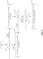
- FIG. 2 depicts a flowchart of an example process for protection against surge events, consistent with embodiments of the present disclosure.
- the process is initially directed to decision block 202 when the process is started. If a selection signal indicates charge mode at decision block 202, a current path is enabled by setting a voltage of a control node ( e.g ., of switching circuit 120) to a first value at block 204. If or when the selection signal is set to indicate a surge protection mode at decision block 202, the current path is disabled by setting a voltage of the control node to a second value at block 206. While the mode selection circuit indicates the surge protection mode, the process is directed from decision block 208 to decision block 210.
- a control node e.g ., of switching circuit 120
- the control node is biased at block 212 ( e.g ., by biasing circuit 110) to prevent the current path from becoming enabled.
- the process is directed back to decision block 208. If or when the selection signal is set to charge mode, the current path is enabled by setting the voltage of the control node to the first value at block 204. The process continues in this manner until the device is reset or powered down.
- FIG. 3 depicts a circuit diagram of an example circuit arrangement for protection against surge events on an IC 300, consistent with embodiments of the present disclosure.
- the circuit arrangement includes a first node 340, a second node 350, a biasing circuit 320, and a switching circuit 330 configured and arranged as described with reference to the first node 130, the second node 140, the biasing circuit 110, and a switching circuit 120 in FIG. 1 .
- the switching circuit 330 includes a number of transistors 332 and 334 arranged to provide a current path between the first and second nodes 340 and 350 responsive to a mode select signal.
- the switching circuit 330 includes two NMOS transistors 332 and 334 connected together in series between the first node 340 and the second node 350.
- the switching circuit 330 may be adapted to provide the current path using a single transistor connected between the first and second nodes 340 and 350 or using three or more transistors connected in a series between the first and second nodes.
- Using multiple series connected in series reduces the sub-threshold leakage current of the current path.
- sub-threshold leakage current reduces at an exponential rate as the number of transistor connected in series is increased.
- two 25 mOhm NMOS transistors connected in series were determined to exhibit a sub-threshold leakage of approximately 0.1 mA, which is sufficient for many applications.
- Each of the NMOS transistors 332 and 334 has a gate connected to receive the mode select signal.
- the IC 300 includes a driver circuit 310 configured to provide the mode select signal to gates of the transistors 332 and 334 of the switching circuit 330.
- the driver circuit 310 in this example includes a respective driver sub-circuit 312 and 314 for each of the transistors 332 and 334.
- the switching circuit When the mode select signal is set at a high voltage (e.g ., logic 1), the switching circuit is operated in a first mode (e.g ., a charging mode), NMOS transistors 332 and 334 are turned on, and the current path is enabled. Conversely, when the mode select signal is set a low value ( e.g ., logic 0), the switching circuit is operated in a second mode (e.g ., a surge protection mode), where transistors 332 and 334 are turned off and the current path is disabled.
- the switching circuit may be operated in the second mode to prevent surge events occurring at node 340, for example, when a power or data cable is initially connected to node 340, from transferring to node 350.
- the switching circuit 330 is resistant to positive surge events when operated in the second mode.
- a positive surge event occurs at node 340
- source voltage of the transistor 332 increases, thereby decreasing the gate-source voltage of the transistor 332.
- the gate-source voltage remains below the threshold voltage and the NMOS transistor remains in an off state.
- the surge current of the positive surge event may be bypassed by one or more additional circuits (not shown in FIG. 3 ) that may be connected to node 340 including, for example, on-chip ESD protection circuits and/or external transient voltage suppression diodes.
- the voltage surge is negative
- the source voltage is decreased and the gate-source voltage is increased. If the gate-source voltage becomes greater than the threshold voltage, the NMOS transistor will switch on and allow the voltage surge to transfer to the transistor 334.
- the negative surge may similarly cause transistor 334 to switch on and allow the surge to transfer to node 350.
- Biasing circuit 320 is configured to bias the control node of the switching circuit to prevent transistor 332 from switching on when negative voltage surge occurs at node 340.
- the biasing circuit 320 includes a NMOS transistor 322 connected in a current path between the gate of transistor 332 and node 340.
- the biasing circuit 320 includes a resistor 324 connecting the gate of the transistor 322 to the driver circuit 310.
- the biasing circuit 320 also includes a resistor 324 connecting the source of transistor 322 to the node 340.
- the gate of transistor 322 is connected to a lower operating voltage of the IC (e.g ., Gnd). During normal operation, transistor 322 is turned off since its gate voltage is tied to Gnd.
- the voltage drop across resistor 324 depends on the resistance of the resistor 324 relative to the resistance of resistor 326.
- the resistors may be selected to have resistivity values sufficient to cause the voltage a drop across resistor 324 to consume the entire operating voltage range of the IC (e.g ., Vdd-Gnd).
- Vdd-Gnd the entire operating voltage range of the IC
- the ability of the driver 310 to provide the mode select signal to transistor 332 may be adversely affected if the resistance of resistor 324 is too high. Simulation and testing of some example circuits have shown that a 4 kOhm resistor 324 and a 20 Ohm resistor 326 provides sufficient voltage drop across resistor 324 without negatively affecting performance during normal operation.
- the circuit arrangement in FIG. 3 has been shown to successfully prevent transfer of both negative surges well outside typical operating voltage ranges for many electronic circuits. For instance, simulation and testing of example implementations of the switching and biasing circuits have been shown to block +/-20V surges generated according to the International Electrotechnical Commission (IEC) 61000-4-5 standard.
- IEC International Electrotechnical Commission
- a mode select signal may be controlled to switch between charging and surge protection modes at various times to protect against surge events.
- the value of the mode select signal may be adjusted, for example by a logic circuit, to prevent transfer of voltage surges when a cable is initially connected.
- the logic circuit may set a mode select signal to cause the switching circuit to operate in surge protection mode until after connection of a cable is detected and any voltage surge has been suppressed. Connection/disconnection of the cable may be detected using various circuits and/or processes. For example, circuit pathway may be completed when a cable terminal is inserted into an input port. As another example, voltage provided by a power cable may be detected ( e.g ., based on a comparison with a reference voltage). In response to verifying that voltage surge is not present, the logic circuit may set the mode select signal to cause the switching circuit to operate in the charge mode.
- the logic circuit may set the mode select signal to switch operation of the switching circuit back to the surge protection mode in response to various events. For example, in some implementations, the logic circuit may monitor voltage of a cable terminal and prompt the switching circuit to operate in the surge protect mode in response to the monitored voltage being indicative of a surge event. As another example, the switching circuit may be prompted to switch from the charging mode to the surge protection mode in response to a battery becoming fully charged or exceeding a rated temperature threshold. As yet another example, if disconnection of the cable is detected, the switching circuit may prompt the switching circuit to again operate in the surge protection mode so voltage surge will be blocked when the cable is reconnected at a later time.
- Embodiments may include features recited in the following numbered clauses.
- an apparatus includes a switching circuit configured to enable a current path between a first node and a second node in a first mode and disable the current path in a second mode.
- a biasing circuit configured to, in the surge protection mode, prevent a voltage surge at the first node from enabling the current path to the second node by biasing a voltage of the control node.
- one or more modules are discrete logic circuits, programmable logic circuits configured and arranged for implementing these operations/activities, or combinations thereof.
- a programmable circuit is one or more computer circuits, including memory circuitry for storing and accessing a program to be executed as a set (or sets) of instructions (and/or to be used as configuration data to define how the programmable circuit is to perform), and an algorithm or process is used by the programmable circuit to perform various steps, functions, operations, activities, etc.
- the instructions (and/or configuration data) can be configured for implementation in logic circuitry, with the instructions (whether characterized in the form of object code, firmware or software) stored in and accessible from a memory (circuit).
Landscapes
- Engineering & Computer Science (AREA)
- Microelectronics & Electronic Packaging (AREA)
- Semiconductor Integrated Circuits (AREA)
- Emergency Protection Circuit Devices (AREA)
Abstract
Description
- Aspects of various embodiments are directed to providing electrostatic discharge protection for electronic circuits. Electrostatic discharge (ESD) may be caused by the sudden flow of electricity that occurs when structures of differing voltage potential become close enough for dielectric between them to break down and facilitate transfer of energy. The differing voltage potential may be created, for example, by the buildup of static electricity between one of the structures (e.g., a cable). One type of ESD, referred to as a cable discharge event or surge event, occurs when charge is transferred from a cable connected to a device. For example, a surge event may occur when a cable that is statically charged to a different potential is connected to a device. When this happens, charge transfers into or out of the device as the voltage potential is reduced. ESD events can damage integrated circuits (ICs) through their connector interfaces. These and other matters have presented challenges to efficiencies of ESD protection implementations, for a variety of applications.
- Various example embodiments are directed to issues such as those addressed above and/or others which may become apparent from the following disclosure concerning electronic circuits. In certain example embodiments, aspects of the present disclosure involve circuits and methods for protecting against voltage surges in electronic devices.
- In certain embodiments, an apparatus includes a switching circuit configured to enable a current path between a first node and a second node in a first mode (e.g., a charging mode) and disable the current path in a second mode (e.g., a surge protection mode). The apparatus further includes a biasing circuit configured to, in the second mode, prevent a voltage surge at the first node from enabling the current path to the second node by biasing a voltage of the control node.
- In a more specific example embodiment, the switching circuit is configured to operate in the first mode in response to a voltage of a control node relative to a voltage of the first node exceeding a threshold voltage and operate in the surge protection mode in response to the voltage of the control node relative to the voltage of the first node being less than the threshold voltage. In the surge protection mode, the switching circuit is configured and arranged disable to prevent a voltage surge at the first node reaching the second node. However, negative surge at the first node may increase the voltage difference between the first node and control node in excess of the threshold voltage and thereby cause the switching circuit to enable the current path. The biasing circuit is configured to prevent a negative surge at the first node from enabling the current path to the second node by biasing the control node to reduce the voltage of the control node.
- In another example embodiment, a method is provided for providing surge protection between first and second nodes. In a first mode, a current path between the first and second nodes is enabled. The current path is enabled by setting a control node of a switching circuit electrically connected in the current path to a first voltage. In a second mode, the current path is disabled by setting the control node to a second voltage. In response to a voltage surge at the first node in the second mode, the switching circuit is prevented from enabling the current path by biasing the voltage of the control node.
- The above discussion/summary is not intended to describe each embodiment or every implementation of the present disclosure. The figures and detailed description that follow also exemplify various embodiments.
- Various example embodiments may be more completely understood in consideration of the following detailed description in connection with the accompanying drawings, in which:
-
FIG. 1 depicts a block diagram of an example circuit for protection against surge events, consistent with embodiments of the present disclosure; -
FIG. 2 depicts a flowchart of an example process for protection against surge events, consistent with embodiments of the present disclosure; and -
FIG. 3 depicts a circuit diagram of an example circuit for protection against surge events, consistent with embodiments of the present disclosure. - While various embodiments discussed herein are amenable to modifications and alternative forms, aspects thereof have been shown by way of example in the drawings and will be described in detail. It should be understood, however, that the intention is not to limit the disclosure to the particular embodiments described. On the contrary, the intention is to cover all modifications, equivalents, and alternatives falling within the scope of the disclosure including aspects defined in the claims. In addition, the term "example" as used throughout this application is only by way of illustration, and not limitation.
- Aspects of the present disclosure are believed to be applicable to a variety of different types of apparatuses, systems, and methods involving electronic circuits. In certain implementations, aspects of the present disclosure have been shown to be beneficial when used in the context of surge protection for electronic circuits. While not necessarily so limited, various aspects may be appreciated through the following discussion of non-limiting examples which use exemplary contexts.
- Methods and circuits are disclosed for protection against positive and/or negative surge events. In certain embodiments, a surge protection circuit includes a switching circuit configured to enable a current path between a first node and a second node in a first mode (e.g., a charging mode) and disable the current path in a second mode (e.g., a surge protection mode). In certain embodiments, the switching circuit is susceptible to inadvertent enabling of the current path in the second mode in response to a surge event which occurs at the first node. The surge protection circuit includes a biasing circuit configured to reduce susceptibility of the switching circuit to the surge event, for example, by biasing a voltage of a node in the switching circuit.
- For some applications, such circuits and methods are used to protect circuitry from positive and/or negative surge events. In a positive voltage surge, a voltage of a node may be shifted above an operating voltage range of a circuit (e.g., greater than a supply voltage). In a negative voltage surge, a voltage of a node may be shifted below the operating voltage range of an integrated circuit (e.g., less than a ground voltage). Certain applications may protect against positive surge events, for example, using a front-end circuit including on-chip ESD protection circuits and/or external transient voltage suppression diodes. However, it can be more difficult to against negative surge events, in which a current/voltage pulse may enter from one touched pin of an IC and exit from another pin of the IC. Certain applications benefitting from aspects of the disclosure reduce susceptibility against such negative surge events.
- As an illustrative example, the switching circuit may include an N-type metal-oxide-semiconductor field-effect transistor (NMOS) transistor required to be off in the second mode in order to ensure correct operation. The NMOS transistor may have a source electrically connected to a node at which a voltage surge is presented. If the voltage surge is positive, the source voltage rises and the gate-source voltage is reduced. As a result, the gate-source voltage remains below the threshold voltage and the NMOS transistor remains in an off state. However, if the voltage surge is negative, the source voltage is decreased and the gate-source voltage is increased. If the gate-source voltage becomes greater than the threshold voltage, the NMOS transistor will switch on and surge may transfer between the first and second nodes.
- In various embodiments, the biasing circuit is configured to prevent the surge event from disrupting correct operation of the switching circuit. For instance, continuing with the above NMOS example, the biasing circuit may be configured to bias a gate of the NMOS transistor when a negative surge occurs to ensure the gate-source voltage remains below the threshold voltage. In this manner, the switching circuit can prevent the negative surge from transferring between the first and second nodes.
- Accordingly, in the following description various specific details are set forth to describe specific examples presented herein. It should be apparent to one skilled in the art, however, that one or more other examples and/or variations of these examples may be practiced without all the specific details given below. In other instances, well known features have not been described in detail so as not to obscure the description of the examples herein. For ease of illustration, the same reference numerals may be used in different diagrams to refer to the same elements or additional instances of the same element. Also, although aspects and features may in some cases be described in individual figures or embodiments, it will be appreciated that features from one figure can be combined with features of another figure or embodiment even though the combination is not explicitly shown or explicitly described as a combination.
- In different embodiments, the switching and biasing circuits may be implemented using various circuits. The circuits may be implemented, for example, using various types of transistor technologies including but not limited to bipolar-junction transistors (BJTs), junction field-effect transistors (JFETs), and/or metal-oxide-semiconductor field-effect transistors MOSFETs. While not so limited, for ease of explanation, the examples are primarily discussed with reference to MOSFETs.
- The disclosed circuits and methods may be useful in various applications to protect against voltage surges. For example, a surge protection circuit may be configured to protect against voltage surges that occur when a power cable (e.g., a USB power line) or a signal line is initially connected to a device. For instance, a surge protection circuit may be used to isolate a USB power line interface connected to a first node from a second node connected to a battery of a device when the USB cable is initially connected. After the cable has been connected and any surge discharged, the surge protection circuit may provide a current path from the power line interface to the battery for charging. As another example, a surge protection circuit may be used to isolate circuits of a device from a data signal line interface of the device (e.g., a headphone jack) when the data signal line is initially connected. A surge protection circuit may additionally or alternatively be configured for protection against voltage surges that are generated on a connected cable during operation, for example, by static electricity, shorted circuit, or lighting strike. For ease of explanation, the examples are primarily discussed in the context of protecting against voltage surge generated when a power cable is connected to a node of a device.
- Turning now to the figures,
FIG. 1 shows an integrated circuit (IC) 100 having a switching circuit connected between afirst node 130 and asecond node 140. In this example, theswitching circuit 120 is configured to enable a current path between thefirst node 130 and thesecond node 140 in response to a mode select signal provided to a control node (Ctrl) indicating a first mode (e.g., a charge/power mode) and disable the current path in response to the mode select signal indicating a second mode (e.g., a surge protection mode). - As previously described, the
switching circuit 120 may be susceptible to one type of surge event (e.g., positive or negative voltage surges). For instance, when a negative voltage surges occur, theswitching circuit 120 may be unable to keep the current path disabled, and thereby may allow current to flow fromnode 140 tonode 130. A biasingcircuit 110 is configured to prevent a voltage surge at the first node from enabling the current path while the switching circuit is operated in the second mode. For example, if theswitching circuit 120 is susceptible to negative voltage surges, the biasingcircuit 110 may be configured to bias the control node Ctrl of theswitching circuit 120 in response to detecting a negative surge event at thefirst node 130. Thebias circuit 110 may detect a negative surge event based on a comparison of the voltage of thefirst node 130 to a reference voltage (e.g., GND). Conversely, if theswitching circuit 120 is susceptible to positive voltage surges, the biasingcircuit 110 may be configured to bias the control node Ctrl of theswitching circuit 120 in response to detecting a positive surge event at thefirst node 130. Thebias circuit 110 may detect a positive surge event based on a comparison of the voltage of thefirst node 130 to a reference voltage (e.g., Vdd). - In a more specific example embodiment, the
switching circuit 120 is configured to enable/disable the current path between the first andsecond nodes first node 130 to a threshold voltage. For instance, theswitching circuit 120 may include a transistor having a gate electrically connected to the control node and a source or drain electrically connected to thefirst node 130. Voltage change induced by a surge event at the first node may shift a voltage of source or drain of the transistor and thereby change the voltage of the gate relative to a voltage of the source/drain of the transistor. The biasingcircuit 110 may be configured to bias the voltage of the control node to prevent a voltage difference between the source and gate from exceeding a threshold voltage at which the transistor begins to pass current. In this manner, the surge event is prevented from causing the transistor from turning on and enabling the current path between the first andsecond nodes -
FIG. 2 depicts a flowchart of an example process for protection against surge events, consistent with embodiments of the present disclosure. The process is initially directed to decision block 202 when the process is started. If a selection signal indicates charge mode atdecision block 202, a current path is enabled by setting a voltage of a control node (e.g., of switching circuit 120) to a first value atblock 204. If or when the selection signal is set to indicate a surge protection mode atdecision block 202, the current path is disabled by setting a voltage of the control node to a second value atblock 206. While the mode selection circuit indicates the surge protection mode, the process is directed fromdecision block 208 todecision block 210. If a surge is present atdecision block 210, the control node is biased at block 212 (e.g., by biasing circuit 110) to prevent the current path from becoming enabled. When the surge is no longer present, the process is directed back todecision block 208. If or when the selection signal is set to charge mode, the current path is enabled by setting the voltage of the control node to the first value atblock 204. The process continues in this manner until the device is reset or powered down. - As previously discussed, the switching and biasing circuit of a surge protection circuit may be implemented using various circuit arrangements.
FIG. 3 depicts a circuit diagram of an example circuit arrangement for protection against surge events on anIC 300, consistent with embodiments of the present disclosure. The circuit arrangement includes afirst node 340, asecond node 350, abiasing circuit 320, and aswitching circuit 330 configured and arranged as described with reference to thefirst node 130, thesecond node 140, the biasingcircuit 110, and aswitching circuit 120 inFIG. 1 . Theswitching circuit 330 includes a number oftransistors second nodes - In this example, the
switching circuit 330 includes twoNMOS transistors first node 340 and thesecond node 350. However, embodiments are not so limited. For instance, theswitching circuit 330 may be adapted to provide the current path using a single transistor connected between the first andsecond nodes - Each of the
NMOS transistors IC 300 includes adriver circuit 310 configured to provide the mode select signal to gates of thetransistors switching circuit 330. Thedriver circuit 310 in this example includes a respective driver sub-circuit 312 and 314 for each of thetransistors - When the mode select signal is set at a high voltage (e.g., logic 1), the switching circuit is operated in a first mode (e.g., a charging mode),
NMOS transistors transistors node 340, for example, when a power or data cable is initially connected tonode 340, from transferring tonode 350. - In this example, the
switching circuit 330 is resistant to positive surge events when operated in the second mode. When a positive surge event occurs atnode 340, source voltage of thetransistor 332 increases, thereby decreasing the gate-source voltage of thetransistor 332. As a result, the gate-source voltage remains below the threshold voltage and the NMOS transistor remains in an off state. The surge current of the positive surge event may be bypassed by one or more additional circuits (not shown inFIG. 3 ) that may be connected tonode 340 including, for example, on-chip ESD protection circuits and/or external transient voltage suppression diodes. Conversely, when the voltage surge is negative, the source voltage is decreased and the gate-source voltage is increased. If the gate-source voltage becomes greater than the threshold voltage, the NMOS transistor will switch on and allow the voltage surge to transfer to thetransistor 334. The negative surge may similarly causetransistor 334 to switch on and allow the surge to transfer tonode 350. -
Biasing circuit 320 is configured to bias the control node of the switching circuit to preventtransistor 332 from switching on when negative voltage surge occurs atnode 340. In this example, the biasingcircuit 320 includes aNMOS transistor 322 connected in a current path between the gate oftransistor 332 andnode 340. The biasingcircuit 320 includes aresistor 324 connecting the gate of thetransistor 322 to thedriver circuit 310. The biasingcircuit 320 also includes aresistor 324 connecting the source oftransistor 322 to thenode 340. The gate oftransistor 322 is connected to a lower operating voltage of the IC (e.g., Gnd). During normal operation,transistor 322 is turned off since its gate voltage is tied to Gnd. When negative voltage surge occurs atnode 340, source voltage oftransistor 322 is pulled well below Gnd. When the gate-source voltage exceeds a threshold voltage of thetransistor 322, thetransistor 322 turns on and provides a current path from the gate oftransistor 332 tonode 340. While thetransistor 322,resistors resistor 324 pull the gate voltage oftransistor 332 to a low voltage sufficient to prevent thetransistor 332 from turning on. In this manner, the switching circuit is able to prevent negative surges from transferring fromnode 340 tonode 350. - The voltage drop across
resistor 324 depends on the resistance of theresistor 324 relative to the resistance ofresistor 326. In some embodiments, the resistors may be selected to have resistivity values sufficient to cause the voltage a drop acrossresistor 324 to consume the entire operating voltage range of the IC (e.g., Vdd-Gnd). As one consideration, it is noted that the ability of thedriver 310 to provide the mode select signal totransistor 332 may be adversely affected if the resistance ofresistor 324 is too high. Simulation and testing of some example circuits have shown that a 4kOhm resistor 324 and a 20Ohm resistor 326 provides sufficient voltage drop acrossresistor 324 without negatively affecting performance during normal operation. - The circuit arrangement in
FIG. 3 has been shown to successfully prevent transfer of both negative surges well outside typical operating voltage ranges for many electronic circuits. For instance, simulation and testing of example implementations of the switching and biasing circuits have been shown to block +/-20V surges generated according to the International Electrotechnical Commission (IEC) 61000-4-5 standard. - In different applications, a mode select signal may be controlled to switch between charging and surge protection modes at various times to protect against surge events. In some embodiments, the value of the mode select signal may be adjusted, for example by a logic circuit, to prevent transfer of voltage surges when a cable is initially connected. As an illustrative example, the logic circuit may set a mode select signal to cause the switching circuit to operate in surge protection mode until after connection of a cable is detected and any voltage surge has been suppressed. Connection/disconnection of the cable may be detected using various circuits and/or processes. For example, circuit pathway may be completed when a cable terminal is inserted into an input port. As another example, voltage provided by a power cable may be detected (e.g., based on a comparison with a reference voltage). In response to verifying that voltage surge is not present, the logic circuit may set the mode select signal to cause the switching circuit to operate in the charge mode.
- The logic circuit may set the mode select signal to switch operation of the switching circuit back to the surge protection mode in response to various events. For example, in some implementations, the logic circuit may monitor voltage of a cable terminal and prompt the switching circuit to operate in the surge protect mode in response to the monitored voltage being indicative of a surge event. As another example, the switching circuit may be prompted to switch from the charging mode to the surge protection mode in response to a battery becoming fully charged or exceeding a rated temperature threshold. As yet another example, if disconnection of the cable is detected, the switching circuit may prompt the switching circuit to again operate in the surge protection mode so voltage surge will be blocked when the cable is reconnected at a later time.
- Embodiments may include features recited in the following numbered clauses.
- 1. An apparatus, comprising: a switching circuit configured and arranged to enable a current path between a first node and a second node in a first mode and disable the current path in a second mode; and a biasing circuit configured to, in a second mode, prevent a voltage surge at the first node from enabling the current path to the second node by biasing a voltage of a control node.
- 2. The apparatus of
clause 1, wherein the switching circuit is configured to operate in the first mode in response to a voltage of a control node relative to a voltage of the first node exceeding a threshold voltage, and operate in the second mode in response to the voltage of the control node relative to the voltage of the first node being less than the threshold voltage, wherein in the second mode the switching circuit is configured and arranged to disable the current path; and the biasing circuit configured to, in the second mode, prevent a negative surge at the first node from enabling the current path to the second node by biasing the control node to reduce the voltage of the control node. - 3. The apparatus of clause 2, wherein the switching circuit includes a transistor having a source and a drain electrically connected in the current path and a gate electrically connected to the control node; the transistor is configured to enable the current path in response to a gate-source voltage exceeding the threshold voltage and disable the current path in response to the gate-source voltage being less than the threshold voltage; and the biasing circuit is configured to reduce the voltage of the gate, in response to the first node having a voltage below an operating voltage range of the switching circuit, by an amount sufficient to prevent the gate-source voltage from exceeding the threshold voltage.
- 4. The apparatus of clause 3, wherein the biasing circuit includes an n-type transistor having a drain electrically connected to the control node, a source electrically connected to the first node, and a gate electrically connected to a ground voltage.
- 5. The apparatus of clause 4, further comprising a driver circuit configured to drive the control node with a mode selection circuit.
- 6. The apparatus of clause 5, wherein the biasing circuit further includes a first resistor having a first end connected to the drain of the n-type transistor and a second end connected to an output of the driver circuit; and a second resistor having a first end connected to the source of the n-type transistor and a second end connected to the first node.
- 7. The apparatus of
clause 1, wherein the switching circuit includes a first transistor and a second transistor connected together in series. - 8. The apparatus of clause 7, wherein the first and second transistors are configured to exhibit a leakage current via the current path that is less than 0.1 mA.
- 9. The apparatus of
clause 1, wherein the switching circuit includes three or more transistors connected together in series. - 10. The apparatus of
clause 1, wherein in the second mode the switching circuit is configured and arranged to prevent negative voltage surges of up to 20V at the first node from reaching the second node. - 11. The apparatus of
clause 1, further comprising a surge protection circuit including the switching and biasing circuits. - 12. A mobile device, comprising: a USB port having a power pin connected to the first node; a battery coupled to the second node; and a circuit protection circuit of clause 11.
- 13. A method, comprising: in a first mode, enabling a current path between a first node and a second node by setting a control node of a switching circuit electrically connected in the current path to a first voltage; and in a second mode, disabling the current path between the first node by setting the control node to a second voltage; and in response to a voltage surge at the first node, preventing the switching circuit from enabling the current path by biasing the voltage of the control node.
- 14. The method of clause 13, wherein the switching circuit includes at least one n-type transistor having a source and a drain electrically connected in the current path and a gate electrically connected to the control node, the n-type transistor being configured to enable the current path in response to a gate-source voltage exceeding a threshold voltage and disable the current path in response to the gate-source voltage falling below the threshold voltage; and the biasing of the voltage of the control node includes reducing the voltage of the control node by an amount sufficient to prevent a gate-source voltage from exceeding the threshold voltage.
- 15. The method of clause 13, wherein the biasing of the voltage is performed using an n-type transistor having a drain electrically connected to the control node, a source electrically connected to the first node, and a gate electrically connected to a ground voltage.
- 16. The method of clause 13, further comprising, operating in the second mode in response to a device including the switching circuit being powered on; and in response to detecting connection of a power supply to the first node determining whether voltage surge is present at the first node, and operating in the first mode after determining that voltage surge is not present at the first node.
- 17. The method of clause 16, further comprising, while operating in the first mode, charging a battery connected to the second node by providing current from the first node to the second node via the current path.
- 18. The method of clause 16, further comprising, operating in the second mode in response to detecting a voltage surge while operating in the first mode.
- 19. The method of clause 16, further comprising, while operating in the first mode, communicating data between the first node and the second node.
- 20. The method of clause 16, wherein the switching circuit includes a first transistor and a second transistor coupled together in series in the current path; and the first and second transistors are configured to exhibit a leakage current via the current path that is less than 0.1 mA.
- Circuits and methods concerning voltage surge protection are disclosed. In an example embodiment, an apparatus includes a switching circuit configured to enable a current path between a first node and a second node in a first mode and disable the current path in a second mode. A biasing circuit configured to, in the surge protection mode, prevent a voltage surge at the first node from enabling the current path to the second node by biasing a voltage of the control node.
- The skilled artisan would recognize that various terminology as used in the Specification (including claims) connote a plain meaning in the art unless otherwise indicated. As examples, the Specification describes and/or illustrates aspects useful for implementing the claimed disclosure by way of various circuits or circuitry which may be illustrated as or using terms such as blocks, modules, device, system, unit, controller, control circuitry and/or other circuit-type depictions (e.g.,
reference numeral 110 ofFIG. 1 depicts a block as described herein). Such circuits or circuitry are used together with other elements to exemplify how certain embodiments may be carried out in the form or structures, steps, functions, operations, activities, etc. For example, in certain of the above-discussed embodiments, one or more modules are discrete logic circuits, programmable logic circuits configured and arranged for implementing these operations/activities, or combinations thereof. In certain embodiments, such a programmable circuit is one or more computer circuits, including memory circuitry for storing and accessing a program to be executed as a set (or sets) of instructions (and/or to be used as configuration data to define how the programmable circuit is to perform), and an algorithm or process is used by the programmable circuit to perform various steps, functions, operations, activities, etc. Depending on the application, the instructions (and/or configuration data) can be configured for implementation in logic circuitry, with the instructions (whether characterized in the form of object code, firmware or software) stored in and accessible from a memory (circuit). - Based upon the above discussion and illustrations, those skilled in the art will readily recognize that various modifications and changes may be made to the various embodiments without strictly following the exemplary embodiments and applications illustrated and described herein. For example, methods as exemplified in the Figures may involve steps carried out in various orders, with one or more aspects of the embodiments herein retained, or may involve fewer or more steps. Such modifications do not depart from the true spirit and scope of various aspects of the disclosure, including aspects set forth in the claims.
Claims (15)
- An apparatus, comprising:a switching circuit configured and arranged to enable a current path between a first node and a second node in a first mode and disable the current path in a second mode; anda biasing circuit configured to, in a second mode, prevent a voltage surge at the first node from enabling the current path to the second node by biasing a voltage of a control node.
- The apparatus of claim 1, wherein
the switching circuit is configured tooperate in the first mode in response to a voltage of a control node relative to a voltage of the first node exceeding a threshold voltage, andoperate in the second mode in response to the voltage of the control node relative to the voltage of the first node being less than the threshold voltage, wherein in the second mode the switching circuit is configured and arranged to disable the current path; andthe biasing circuit configured to, in the second mode, prevent a negative surge at the first node from enabling the current path to the second node by biasing the control node to reduce the voltage of the control node. - The apparatus of any preceding claim, wherein
the switching circuit includes a transistor having a source and a drain electrically connected in the current path and a gate electrically connected to the control node;
the transistor is configured to enable the current path in response to a gate-source voltage exceeding the threshold voltage and disable the current path in response to the gate-source voltage being less than the threshold voltage; and
the biasing circuit is configured to reduce the voltage of the gate, in response to the first node having a voltage below an operating voltage range of the switching circuit, by an amount sufficient to prevent the gate-source voltage from exceeding the threshold voltage. - The apparatus of claim 3, wherein
the biasing circuit includes an n-type transistor having a drain electrically connected to the control node, a source electrically connected to the first node, and a gate electrically connected to a ground voltage. - The apparatus of claim 4, further comprising a driver circuit configured to drive the control node with a mode selection circuit.
- The apparatus of claim 5, wherein the biasing circuit further includes
a first resistor having a first end connected to the drain of the n-type transistor and a second end connected to an output of the driver circuit; and
a second resistor having a first end connected to the source of the n-type transistor and a second end connected to the first node. - The apparatus of any preceding claim, wherein the switching circuit includes a first transistor and a second transistor connected together in series.
- The apparatus of claim 7, wherein the first and second transistors are configured to exhibit a leakage current via the current path that is less than 0.1 mA.
- The apparatus of any preceding claim, wherein the switching circuit includes three or more transistors connected together in series.
- The apparatus of any preceding claim, wherein in the second mode the switching circuit is configured and arranged to prevent negative voltage surges of up to 20V at the first node from reaching the second node.
- The apparatus of any preceding claim, further comprising a surge protection circuit including the switching and biasing circuits.
- A mobile device, comprising:a USB port having a power pin connected to the first node;a battery coupled to the second node; anda circuit protection circuit of claim 11.
- A method, comprising:in a first mode, enabling a current path between a first node and a second node by setting a control node of a switching circuit electrically connected in the current path to a first voltage; andin a second mode,disabling the current path between the first node by setting the control node to a second voltage; andin response to a voltage surge at the first node, preventing the switching circuit from enabling the current path by biasing the voltage of the control node.
- The method of claim 13, wherein
the switching circuit includes at least one n-type transistor having a source and a drain electrically connected in the current path and a gate electrically connected to the control node, the n-type transistor being configured to enable the current path in response to a gate-source voltage exceeding a threshold voltage and disable the current path in response to the gate-source voltage falling below the threshold voltage; and
the biasing of the voltage of the control node includes reducing the voltage of the control node by an amount sufficient to prevent a gate-source voltage from exceeding the threshold voltage. - The method of claim 13 or 14, wherein the biasing of the voltage is performed using an n-type transistor having a drain electrically connected to the control node, a source electrically connected to the first node, and a gate electrically connected to a ground voltage.
Applications Claiming Priority (1)
| Application Number | Priority Date | Filing Date | Title |
|---|---|---|---|
| US15/083,699 US10164425B2 (en) | 2016-03-29 | 2016-03-29 | Electrostatic discharge protection |
Publications (2)
| Publication Number | Publication Date |
|---|---|
| EP3226296A1 true EP3226296A1 (en) | 2017-10-04 |
| EP3226296B1 EP3226296B1 (en) | 2019-10-16 |
Family
ID=58213012
Family Applications (1)
| Application Number | Title | Priority Date | Filing Date |
|---|---|---|---|
| EP17158886.6A Active EP3226296B1 (en) | 2016-03-29 | 2017-03-02 | Electrostatic discharge protection |
Country Status (3)
| Country | Link |
|---|---|
| US (1) | US10164425B2 (en) |
| EP (1) | EP3226296B1 (en) |
| CN (1) | CN107240913B (en) |
Families Citing this family (3)
| Publication number | Priority date | Publication date | Assignee | Title |
|---|---|---|---|---|
| FR3069388B1 (en) * | 2017-07-24 | 2020-01-17 | STMicroelectronics (Alps) SAS | METHOD FOR CONTROLLING INTERIOR CURRENTS THAT MAY BE CIRCULATED IN A CHARGE SWITCH, AND CORRESPONDING ELECTRONIC CIRCUIT |
| CN213717633U (en) * | 2019-12-30 | 2021-07-16 | 华为技术有限公司 | Charging protection circuit, charging circuit and electronic equipment |
| CN116435976B (en) * | 2023-06-12 | 2023-11-03 | 上海维安半导体有限公司 | Withstand voltage type surge protection device |
Citations (4)
| Publication number | Priority date | Publication date | Assignee | Title |
|---|---|---|---|---|
| US5517379A (en) * | 1993-05-26 | 1996-05-14 | Siliconix Incorporated | Reverse battery protection device containing power MOSFET |
| EP0854555A2 (en) * | 1996-12-21 | 1998-07-22 | STMicroelectronics, Inc. | Integrated supply protection |
| US20070139836A1 (en) * | 2005-12-09 | 2007-06-21 | Yuuichi Ueda | Backflow preventing circuit capable of preventing reverse current efficiently |
| US20130063844A1 (en) * | 2011-09-14 | 2013-03-14 | Fairchild Semiconductor Corporation | Load Switch with True Reverse Current Blocking |
Family Cites Families (8)
| Publication number | Priority date | Publication date | Assignee | Title |
|---|---|---|---|---|
| KR100206870B1 (en) * | 1995-11-28 | 1999-07-01 | 구본준 | Electrostatic Discharge and Latch-Up Protection Circuit |
| US6191606B1 (en) * | 1998-09-10 | 2001-02-20 | Intel Corporation | Method and apparatus for reducing standby leakage current using input vector activation |
| US6738242B1 (en) * | 2002-03-07 | 2004-05-18 | Pericom Semiconductor Corp. | ESD-isolation circuit driving gate of bus-switch transistor during ESD pulse between two I/O pins |
| US20050224882A1 (en) | 2004-04-08 | 2005-10-13 | International Business Machines Corporation | Low trigger voltage esd nmosfet triple-well cmos devices |
| US7098513B2 (en) | 2005-01-17 | 2006-08-29 | International Business Machines Corporation | Low trigger voltage, low leakage ESD NFET |
| US7268398B1 (en) | 2006-08-14 | 2007-09-11 | National Semiconductor Corporation | ESD protection cell with active pwell resistance control |
| US7581970B2 (en) * | 2007-11-16 | 2009-09-01 | Sony Ericsson Mobile Communications Ab | Multipurpose universal serial bus cable |
| US8067996B2 (en) | 2008-11-14 | 2011-11-29 | Teledyne Scientific & Imaging, Llc | Vanadium-dioxide front-end advanced shutter technology |
-
2016
- 2016-03-29 US US15/083,699 patent/US10164425B2/en active Active
-
2017
- 2017-03-02 EP EP17158886.6A patent/EP3226296B1/en active Active
- 2017-03-28 CN CN201710194817.0A patent/CN107240913B/en active Active
Patent Citations (4)
| Publication number | Priority date | Publication date | Assignee | Title |
|---|---|---|---|---|
| US5517379A (en) * | 1993-05-26 | 1996-05-14 | Siliconix Incorporated | Reverse battery protection device containing power MOSFET |
| EP0854555A2 (en) * | 1996-12-21 | 1998-07-22 | STMicroelectronics, Inc. | Integrated supply protection |
| US20070139836A1 (en) * | 2005-12-09 | 2007-06-21 | Yuuichi Ueda | Backflow preventing circuit capable of preventing reverse current efficiently |
| US20130063844A1 (en) * | 2011-09-14 | 2013-03-14 | Fairchild Semiconductor Corporation | Load Switch with True Reverse Current Blocking |
Also Published As
| Publication number | Publication date |
|---|---|
| US20170288397A1 (en) | 2017-10-05 |
| CN107240913A (en) | 2017-10-10 |
| EP3226296B1 (en) | 2019-10-16 |
| US10164425B2 (en) | 2018-12-25 |
| CN107240913B (en) | 2020-11-10 |
Similar Documents
| Publication | Publication Date | Title |
|---|---|---|
| CN101800424B (en) | ESD protection using capacitively coupled clamp circuits for protecting low voltage core transistors from high voltage output | |
| US9401594B2 (en) | Surge protection for differential input/output interfaces | |
| EP3484002B1 (en) | Electrostatic protection circuit | |
| CN113848504B (en) | Port controller power path short circuit detection | |
| KR102614993B1 (en) | Charging circuit and electronics | |
| US9627885B2 (en) | Electrostatic discharge protection circuit | |
| US20200036182A1 (en) | Fast over voltage and surge detection for high speed and load switches | |
| CN101931204B (en) | Overload protection device and method | |
| US20190245341A1 (en) | Over voltage/energy protection apparatus | |
| EP3226296B1 (en) | Electrostatic discharge protection | |
| EP3300110A1 (en) | Integrated circuit with protection from transient electrical stress events and method therefor | |
| US7872840B1 (en) | Erase pin protection in EEPROM using active snapback ESD device with positive feedback and shutdown | |
| CN111106597B (en) | Power switch overcurrent protection system | |
| CN106058798B (en) | Voltage protection device, method and wearable device | |
| EP3432434A1 (en) | Voltage clamp circuit for surge protection | |
| CN108400781B (en) | Power switching device and operation method thereof | |
| CN111739458A (en) | Drive circuit and display drive chip | |
| CN100459358C (en) | Circuit arrangement for protecting integrated circuits from electrostatic discharge | |
| WO2013141864A1 (en) | Electrostatic discharge clamp compatible with a fast ramping supply | |
| CN115566635A (en) | Overvoltage detection and protection | |
| US9762052B2 (en) | Circuit and method of electrically decoupling nodes | |
| TWI641221B (en) | Interface circuit of an electronic device | |
| US7656628B2 (en) | Apparatus for providing fault protection in a circuit supplying power to an electronic device | |
| JP5143096B2 (en) | Protection circuit | |
| CN110138375B (en) | Circuit for chip pin |
Legal Events
| Date | Code | Title | Description |
|---|---|---|---|
| PUAI | Public reference made under article 153(3) epc to a published international application that has entered the european phase |
Free format text: ORIGINAL CODE: 0009012 |
|
| STAA | Information on the status of an ep patent application or granted ep patent |
Free format text: STATUS: THE APPLICATION HAS BEEN PUBLISHED |
|
| AK | Designated contracting states |
Kind code of ref document: A1 Designated state(s): AL AT BE BG CH CY CZ DE DK EE ES FI FR GB GR HR HU IE IS IT LI LT LU LV MC MK MT NL NO PL PT RO RS SE SI SK SM TR |
|
| AX | Request for extension of the european patent |
Extension state: BA ME |
|
| STAA | Information on the status of an ep patent application or granted ep patent |
Free format text: STATUS: REQUEST FOR EXAMINATION WAS MADE |
|
| 17P | Request for examination filed |
Effective date: 20180404 |
|
| RBV | Designated contracting states (corrected) |
Designated state(s): AL AT BE BG CH CY CZ DE DK EE ES FI FR GB GR HR HU IE IS IT LI LT LU LV MC MK MT NL NO PL PT RO RS SE SI SK SM TR |
|
| STAA | Information on the status of an ep patent application or granted ep patent |
Free format text: STATUS: EXAMINATION IS IN PROGRESS |
|
| 17Q | First examination report despatched |
Effective date: 20181004 |
|
| GRAP | Despatch of communication of intention to grant a patent |
Free format text: ORIGINAL CODE: EPIDOSNIGR1 |
|
| STAA | Information on the status of an ep patent application or granted ep patent |
Free format text: STATUS: GRANT OF PATENT IS INTENDED |
|
| INTG | Intention to grant announced |
Effective date: 20190606 |
|
| GRAS | Grant fee paid |
Free format text: ORIGINAL CODE: EPIDOSNIGR3 |
|
| GRAA | (expected) grant |
Free format text: ORIGINAL CODE: 0009210 |
|
| STAA | Information on the status of an ep patent application or granted ep patent |
Free format text: STATUS: THE PATENT HAS BEEN GRANTED |
|
| AK | Designated contracting states |
Kind code of ref document: B1 Designated state(s): AL AT BE BG CH CY CZ DE DK EE ES FI FR GB GR HR HU IE IS IT LI LT LU LV MC MK MT NL NO PL PT RO RS SE SI SK SM TR |
|
| REG | Reference to a national code |
Ref country code: GB Ref legal event code: FG4D |
|
| REG | Reference to a national code |
Ref country code: CH Ref legal event code: EP |
|
| REG | Reference to a national code |
Ref country code: DE Ref legal event code: R096 Ref document number: 602017007751 Country of ref document: DE |
|
| REG | Reference to a national code |
Ref country code: IE Ref legal event code: FG4D |
|
| REG | Reference to a national code |
Ref country code: AT Ref legal event code: REF Ref document number: 1192131 Country of ref document: AT Kind code of ref document: T Effective date: 20191115 |
|
| REG | Reference to a national code |
Ref country code: NL Ref legal event code: MP Effective date: 20191016 |
|
| REG | Reference to a national code |
Ref country code: LT Ref legal event code: MG4D |
|
| REG | Reference to a national code |
Ref country code: AT Ref legal event code: MK05 Ref document number: 1192131 Country of ref document: AT Kind code of ref document: T Effective date: 20191016 |
|
| PG25 | Lapsed in a contracting state [announced via postgrant information from national office to epo] |
Ref country code: PT Free format text: LAPSE BECAUSE OF FAILURE TO SUBMIT A TRANSLATION OF THE DESCRIPTION OR TO PAY THE FEE WITHIN THE PRESCRIBED TIME-LIMIT Effective date: 20200217 Ref country code: LT Free format text: LAPSE BECAUSE OF FAILURE TO SUBMIT A TRANSLATION OF THE DESCRIPTION OR TO PAY THE FEE WITHIN THE PRESCRIBED TIME-LIMIT Effective date: 20191016 Ref country code: NL Free format text: LAPSE BECAUSE OF FAILURE TO SUBMIT A TRANSLATION OF THE DESCRIPTION OR TO PAY THE FEE WITHIN THE PRESCRIBED TIME-LIMIT Effective date: 20191016 Ref country code: AT Free format text: LAPSE BECAUSE OF FAILURE TO SUBMIT A TRANSLATION OF THE DESCRIPTION OR TO PAY THE FEE WITHIN THE PRESCRIBED TIME-LIMIT Effective date: 20191016 Ref country code: SE Free format text: LAPSE BECAUSE OF FAILURE TO SUBMIT A TRANSLATION OF THE DESCRIPTION OR TO PAY THE FEE WITHIN THE PRESCRIBED TIME-LIMIT Effective date: 20191016 Ref country code: LV Free format text: LAPSE BECAUSE OF FAILURE TO SUBMIT A TRANSLATION OF THE DESCRIPTION OR TO PAY THE FEE WITHIN THE PRESCRIBED TIME-LIMIT Effective date: 20191016 Ref country code: GR Free format text: LAPSE BECAUSE OF FAILURE TO SUBMIT A TRANSLATION OF THE DESCRIPTION OR TO PAY THE FEE WITHIN THE PRESCRIBED TIME-LIMIT Effective date: 20200117 Ref country code: PL Free format text: LAPSE BECAUSE OF FAILURE TO SUBMIT A TRANSLATION OF THE DESCRIPTION OR TO PAY THE FEE WITHIN THE PRESCRIBED TIME-LIMIT Effective date: 20191016 Ref country code: BG Free format text: LAPSE BECAUSE OF FAILURE TO SUBMIT A TRANSLATION OF THE DESCRIPTION OR TO PAY THE FEE WITHIN THE PRESCRIBED TIME-LIMIT Effective date: 20200116 Ref country code: NO Free format text: LAPSE BECAUSE OF FAILURE TO SUBMIT A TRANSLATION OF THE DESCRIPTION OR TO PAY THE FEE WITHIN THE PRESCRIBED TIME-LIMIT Effective date: 20200116 Ref country code: FI Free format text: LAPSE BECAUSE OF FAILURE TO SUBMIT A TRANSLATION OF THE DESCRIPTION OR TO PAY THE FEE WITHIN THE PRESCRIBED TIME-LIMIT Effective date: 20191016 |
|
| PG25 | Lapsed in a contracting state [announced via postgrant information from national office to epo] |
Ref country code: RS Free format text: LAPSE BECAUSE OF FAILURE TO SUBMIT A TRANSLATION OF THE DESCRIPTION OR TO PAY THE FEE WITHIN THE PRESCRIBED TIME-LIMIT Effective date: 20191016 Ref country code: HR Free format text: LAPSE BECAUSE OF FAILURE TO SUBMIT A TRANSLATION OF THE DESCRIPTION OR TO PAY THE FEE WITHIN THE PRESCRIBED TIME-LIMIT Effective date: 20191016 Ref country code: IS Free format text: LAPSE BECAUSE OF FAILURE TO SUBMIT A TRANSLATION OF THE DESCRIPTION OR TO PAY THE FEE WITHIN THE PRESCRIBED TIME-LIMIT Effective date: 20200224 |
|
| PG25 | Lapsed in a contracting state [announced via postgrant information from national office to epo] |
Ref country code: AL Free format text: LAPSE BECAUSE OF FAILURE TO SUBMIT A TRANSLATION OF THE DESCRIPTION OR TO PAY THE FEE WITHIN THE PRESCRIBED TIME-LIMIT Effective date: 20191016 |
|
| REG | Reference to a national code |
Ref country code: DE Ref legal event code: R097 Ref document number: 602017007751 Country of ref document: DE |
|
| PG2D | Information on lapse in contracting state deleted |
Ref country code: IS |
|
| PG25 | Lapsed in a contracting state [announced via postgrant information from national office to epo] |
Ref country code: DK Free format text: LAPSE BECAUSE OF FAILURE TO SUBMIT A TRANSLATION OF THE DESCRIPTION OR TO PAY THE FEE WITHIN THE PRESCRIBED TIME-LIMIT Effective date: 20191016 Ref country code: CZ Free format text: LAPSE BECAUSE OF FAILURE TO SUBMIT A TRANSLATION OF THE DESCRIPTION OR TO PAY THE FEE WITHIN THE PRESCRIBED TIME-LIMIT Effective date: 20191016 Ref country code: ES Free format text: LAPSE BECAUSE OF FAILURE TO SUBMIT A TRANSLATION OF THE DESCRIPTION OR TO PAY THE FEE WITHIN THE PRESCRIBED TIME-LIMIT Effective date: 20191016 Ref country code: RO Free format text: LAPSE BECAUSE OF FAILURE TO SUBMIT A TRANSLATION OF THE DESCRIPTION OR TO PAY THE FEE WITHIN THE PRESCRIBED TIME-LIMIT Effective date: 20191016 Ref country code: EE Free format text: LAPSE BECAUSE OF FAILURE TO SUBMIT A TRANSLATION OF THE DESCRIPTION OR TO PAY THE FEE WITHIN THE PRESCRIBED TIME-LIMIT Effective date: 20191016 Ref country code: IS Free format text: LAPSE BECAUSE OF FAILURE TO SUBMIT A TRANSLATION OF THE DESCRIPTION OR TO PAY THE FEE WITHIN THE PRESCRIBED TIME-LIMIT Effective date: 20200216 |
|
| PLBE | No opposition filed within time limit |
Free format text: ORIGINAL CODE: 0009261 |
|
| STAA | Information on the status of an ep patent application or granted ep patent |
Free format text: STATUS: NO OPPOSITION FILED WITHIN TIME LIMIT |
|
| PG25 | Lapsed in a contracting state [announced via postgrant information from national office to epo] |
Ref country code: SK Free format text: LAPSE BECAUSE OF FAILURE TO SUBMIT A TRANSLATION OF THE DESCRIPTION OR TO PAY THE FEE WITHIN THE PRESCRIBED TIME-LIMIT Effective date: 20191016 Ref country code: IT Free format text: LAPSE BECAUSE OF FAILURE TO SUBMIT A TRANSLATION OF THE DESCRIPTION OR TO PAY THE FEE WITHIN THE PRESCRIBED TIME-LIMIT Effective date: 20191016 Ref country code: SM Free format text: LAPSE BECAUSE OF FAILURE TO SUBMIT A TRANSLATION OF THE DESCRIPTION OR TO PAY THE FEE WITHIN THE PRESCRIBED TIME-LIMIT Effective date: 20191016 |
|
| 26N | No opposition filed |
Effective date: 20200717 |
|
| PG25 | Lapsed in a contracting state [announced via postgrant information from national office to epo] |
Ref country code: MC Free format text: LAPSE BECAUSE OF FAILURE TO SUBMIT A TRANSLATION OF THE DESCRIPTION OR TO PAY THE FEE WITHIN THE PRESCRIBED TIME-LIMIT Effective date: 20191016 |
|
| REG | Reference to a national code |
Ref country code: CH Ref legal event code: PL |
|
| PG25 | Lapsed in a contracting state [announced via postgrant information from national office to epo] |
Ref country code: SI Free format text: LAPSE BECAUSE OF FAILURE TO SUBMIT A TRANSLATION OF THE DESCRIPTION OR TO PAY THE FEE WITHIN THE PRESCRIBED TIME-LIMIT Effective date: 20191016 |
|
| REG | Reference to a national code |
Ref country code: BE Ref legal event code: MM Effective date: 20200331 |
|
| PG25 | Lapsed in a contracting state [announced via postgrant information from national office to epo] |
Ref country code: LU Free format text: LAPSE BECAUSE OF NON-PAYMENT OF DUE FEES Effective date: 20200302 |
|
| PG25 | Lapsed in a contracting state [announced via postgrant information from national office to epo] |
Ref country code: LI Free format text: LAPSE BECAUSE OF NON-PAYMENT OF DUE FEES Effective date: 20200331 Ref country code: CH Free format text: LAPSE BECAUSE OF NON-PAYMENT OF DUE FEES Effective date: 20200331 Ref country code: IE Free format text: LAPSE BECAUSE OF NON-PAYMENT OF DUE FEES Effective date: 20200302 |
|
| PG25 | Lapsed in a contracting state [announced via postgrant information from national office to epo] |
Ref country code: BE Free format text: LAPSE BECAUSE OF NON-PAYMENT OF DUE FEES Effective date: 20200331 |
|
| GBPC | Gb: european patent ceased through non-payment of renewal fee |
Effective date: 20210302 |
|
| PG25 | Lapsed in a contracting state [announced via postgrant information from national office to epo] |
Ref country code: GB Free format text: LAPSE BECAUSE OF NON-PAYMENT OF DUE FEES Effective date: 20210302 |
|
| PG25 | Lapsed in a contracting state [announced via postgrant information from national office to epo] |
Ref country code: TR Free format text: LAPSE BECAUSE OF FAILURE TO SUBMIT A TRANSLATION OF THE DESCRIPTION OR TO PAY THE FEE WITHIN THE PRESCRIBED TIME-LIMIT Effective date: 20191016 Ref country code: MT Free format text: LAPSE BECAUSE OF FAILURE TO SUBMIT A TRANSLATION OF THE DESCRIPTION OR TO PAY THE FEE WITHIN THE PRESCRIBED TIME-LIMIT Effective date: 20191016 Ref country code: CY Free format text: LAPSE BECAUSE OF FAILURE TO SUBMIT A TRANSLATION OF THE DESCRIPTION OR TO PAY THE FEE WITHIN THE PRESCRIBED TIME-LIMIT Effective date: 20191016 |
|
| PG25 | Lapsed in a contracting state [announced via postgrant information from national office to epo] |
Ref country code: MK Free format text: LAPSE BECAUSE OF FAILURE TO SUBMIT A TRANSLATION OF THE DESCRIPTION OR TO PAY THE FEE WITHIN THE PRESCRIBED TIME-LIMIT Effective date: 20191016 |
|
| P01 | Opt-out of the competence of the unified patent court (upc) registered |
Effective date: 20230725 |
|
| REG | Reference to a national code |
Ref country code: DE Ref legal event code: R079 Ref document number: 602017007751 Country of ref document: DE Free format text: PREVIOUS MAIN CLASS: H01L0027020000 Ipc: H10D0089000000 |
|
| PGFP | Annual fee paid to national office [announced via postgrant information from national office to epo] |
Ref country code: DE Payment date: 20260219 Year of fee payment: 10 |
|
| PGFP | Annual fee paid to national office [announced via postgrant information from national office to epo] |
Ref country code: FR Payment date: 20260219 Year of fee payment: 10 |