EP3226052A1 - Camera assembly for use on a vehicle - Google Patents
Camera assembly for use on a vehicle Download PDFInfo
- Publication number
- EP3226052A1 EP3226052A1 EP17161891.1A EP17161891A EP3226052A1 EP 3226052 A1 EP3226052 A1 EP 3226052A1 EP 17161891 A EP17161891 A EP 17161891A EP 3226052 A1 EP3226052 A1 EP 3226052A1
- Authority
- EP
- European Patent Office
- Prior art keywords
- sensor
- lens
- camera assembly
- lens elements
- infrared cut
- Prior art date
- Legal status (The legal status is an assumption and is not a legal conclusion. Google has not performed a legal analysis and makes no representation as to the accuracy of the status listed.)
- Withdrawn
Links
- 230000005855 radiation Effects 0.000 claims abstract description 14
- 238000013459 approach Methods 0.000 claims abstract description 4
- 238000000034 method Methods 0.000 claims description 16
- 239000000758 substrate Substances 0.000 claims description 12
- 230000005499 meniscus Effects 0.000 claims description 3
- 238000012937 correction Methods 0.000 claims description 2
- 238000004519 manufacturing process Methods 0.000 claims description 2
- 238000001228 spectrum Methods 0.000 claims description 2
- 230000008901 benefit Effects 0.000 description 2
- 238000005516 engineering process Methods 0.000 description 2
- 230000008569 process Effects 0.000 description 2
- 230000000712 assembly Effects 0.000 description 1
- 238000000429 assembly Methods 0.000 description 1
- 230000008859 change Effects 0.000 description 1
- 239000011248 coating agent Substances 0.000 description 1
- 238000000576 coating method Methods 0.000 description 1
- 238000013461 design Methods 0.000 description 1
- 239000012467 final product Substances 0.000 description 1
- 238000003384 imaging method Methods 0.000 description 1
- 239000000463 material Substances 0.000 description 1
- 238000010295 mobile communication Methods 0.000 description 1
- 238000012986 modification Methods 0.000 description 1
- 230000004048 modification Effects 0.000 description 1
- 230000003287 optical effect Effects 0.000 description 1
- 238000004806 packaging method and process Methods 0.000 description 1
- 230000035755 proliferation Effects 0.000 description 1
Images

Classifications
-
- G—PHYSICS
- G02—OPTICS
- G02B—OPTICAL ELEMENTS, SYSTEMS OR APPARATUS
- G02B5/00—Optical elements other than lenses
- G02B5/20—Filters
- G02B5/208—Filters for use with infrared or ultraviolet radiation, e.g. for separating visible light from infrared and/or ultraviolet radiation
-
- G—PHYSICS
- G03—PHOTOGRAPHY; CINEMATOGRAPHY; ANALOGOUS TECHNIQUES USING WAVES OTHER THAN OPTICAL WAVES; ELECTROGRAPHY; HOLOGRAPHY
- G03B—APPARATUS OR ARRANGEMENTS FOR TAKING PHOTOGRAPHS OR FOR PROJECTING OR VIEWING THEM; APPARATUS OR ARRANGEMENTS EMPLOYING ANALOGOUS TECHNIQUES USING WAVES OTHER THAN OPTICAL WAVES; ACCESSORIES THEREFOR
- G03B17/00—Details of cameras or camera bodies; Accessories therefor
- G03B17/02—Bodies
- G03B17/12—Bodies with means for supporting objectives, supplementary lenses, filters, masks, or turrets
-
- G—PHYSICS
- G02—OPTICS
- G02B—OPTICAL ELEMENTS, SYSTEMS OR APPARATUS
- G02B9/00—Optical objectives characterised both by the number of the components and their arrangements according to their sign, i.e. + or -
- G02B9/34—Optical objectives characterised both by the number of the components and their arrangements according to their sign, i.e. + or - having four components only
-
- G—PHYSICS
- G02—OPTICS
- G02B—OPTICAL ELEMENTS, SYSTEMS OR APPARATUS
- G02B13/00—Optical objectives specially designed for the purposes specified below
- G02B13/001—Miniaturised objectives for electronic devices, e.g. portable telephones, webcams, PDAs, small digital cameras
- G02B13/0015—Miniaturised objectives for electronic devices, e.g. portable telephones, webcams, PDAs, small digital cameras characterised by the lens design
- G02B13/002—Miniaturised objectives for electronic devices, e.g. portable telephones, webcams, PDAs, small digital cameras characterised by the lens design having at least one aspherical surface
-
- G—PHYSICS
- G02—OPTICS
- G02B—OPTICAL ELEMENTS, SYSTEMS OR APPARATUS
- G02B13/00—Optical objectives specially designed for the purposes specified below
- G02B13/001—Miniaturised objectives for electronic devices, e.g. portable telephones, webcams, PDAs, small digital cameras
- G02B13/0015—Miniaturised objectives for electronic devices, e.g. portable telephones, webcams, PDAs, small digital cameras characterised by the lens design
- G02B13/002—Miniaturised objectives for electronic devices, e.g. portable telephones, webcams, PDAs, small digital cameras characterised by the lens design having at least one aspherical surface
- G02B13/004—Miniaturised objectives for electronic devices, e.g. portable telephones, webcams, PDAs, small digital cameras characterised by the lens design having at least one aspherical surface having four lenses
-
- G—PHYSICS
- G02—OPTICS
- G02B—OPTICAL ELEMENTS, SYSTEMS OR APPARATUS
- G02B13/00—Optical objectives specially designed for the purposes specified below
- G02B13/001—Miniaturised objectives for electronic devices, e.g. portable telephones, webcams, PDAs, small digital cameras
- G02B13/0055—Miniaturised objectives for electronic devices, e.g. portable telephones, webcams, PDAs, small digital cameras employing a special optical element
- G02B13/006—Miniaturised objectives for electronic devices, e.g. portable telephones, webcams, PDAs, small digital cameras employing a special optical element at least one element being a compound optical element, e.g. cemented elements
-
- G—PHYSICS
- G02—OPTICS
- G02B—OPTICAL ELEMENTS, SYSTEMS OR APPARATUS
- G02B3/00—Simple or compound lenses
- G02B3/0006—Arrays
- G02B3/0037—Arrays characterized by the distribution or form of lenses
- G02B3/0043—Inhomogeneous or irregular arrays, e.g. varying shape, size, height
-
- G—PHYSICS
- G02—OPTICS
- G02B—OPTICAL ELEMENTS, SYSTEMS OR APPARATUS
- G02B3/00—Simple or compound lenses
- G02B3/0006—Arrays
- G02B3/0037—Arrays characterized by the distribution or form of lenses
- G02B3/0062—Stacked lens arrays, i.e. refractive surfaces arranged in at least two planes, without structurally separate optical elements in-between
-
- G—PHYSICS
- G02—OPTICS
- G02B—OPTICAL ELEMENTS, SYSTEMS OR APPARATUS
- G02B7/00—Mountings, adjusting means, or light-tight connections, for optical elements
- G02B7/006—Filter holders
-
- G—PHYSICS
- G02—OPTICS
- G02B—OPTICAL ELEMENTS, SYSTEMS OR APPARATUS
- G02B7/00—Mountings, adjusting means, or light-tight connections, for optical elements
- G02B7/02—Mountings, adjusting means, or light-tight connections, for optical elements for lenses
- G02B7/021—Mountings, adjusting means, or light-tight connections, for optical elements for lenses for more than one lens
-
- H—ELECTRICITY
- H04—ELECTRIC COMMUNICATION TECHNIQUE
- H04N—PICTORIAL COMMUNICATION, e.g. TELEVISION
- H04N23/00—Cameras or camera modules comprising electronic image sensors; Control thereof
- H04N23/50—Constructional details
-
- H—ELECTRICITY
- H04—ELECTRIC COMMUNICATION TECHNIQUE
- H04N—PICTORIAL COMMUNICATION, e.g. TELEVISION
- H04N23/00—Cameras or camera modules comprising electronic image sensors; Control thereof
- H04N23/50—Constructional details
- H04N23/51—Housings
-
- H—ELECTRICITY
- H04—ELECTRIC COMMUNICATION TECHNIQUE
- H04N—PICTORIAL COMMUNICATION, e.g. TELEVISION
- H04N23/00—Cameras or camera modules comprising electronic image sensors; Control thereof
- H04N23/50—Constructional details
- H04N23/54—Mounting of pick-up tubes, electronic image sensors, deviation or focusing coils
-
- G—PHYSICS
- G02—OPTICS
- G02B—OPTICAL ELEMENTS, SYSTEMS OR APPARATUS
- G02B5/00—Optical elements other than lenses
- G02B5/20—Filters
- G02B5/28—Interference filters
- G02B5/281—Interference filters designed for the infrared light
- G02B5/282—Interference filters designed for the infrared light reflecting for infrared and transparent for visible light, e.g. heat reflectors, laser protection
Definitions
- the subject matter of this disclosure generally relates to cameras. More specifically, and without limitation, the subject matter of this disclosure pertains to a camera assembly including an infrared cut filter that is useful on an automotive vehicle.
- an infrared filter is useful on cameras for providing better image quality especially in daylight conditions.
- the known way of incorporating an infrared filter into a camera presents challenges when attempting to limit the size of a camera assembly.
- the presence of an infrared filter tends to increase the back focal distance between a sensor and the lens element closest to that sensor. It is also difficult to limit the total track length of the camera.
- Some attempts to achieve a shorter total track length require introducing a relatively large number of aspherical lens surfaces, which tends to complicate the design and introduce undesired additional cost.
- An illustrative example camera assembly includes a sensor.
- An infrared cut filter is situated to filter radiation as the radiation approaches the sensor.
- a plurality of lens elements is situated between the sensor and the infrared cut filter.
- An illustrative example method of making a camera assembly includes supporting a plurality of lens elements within a housing.
- a sensor is positioned near one end of the housing.
- An infrared cut filter is positioned near an opposite end of the housing with the plurality of lens elements between the infrared cut filter and the sensor.
- the sensor is situated adjacent a circuit board substrate and the sensor and the housing are secured to the circuit board substrate using a surface mount technique.
- Figure 1 schematically illustrates a camera assembly 20.
- a sensor 22 is configured to detect radiation and provide an output that may be processed using known techniques for generating an image.
- the sensor 22 may be configured for detecting radiation in the visible light spectrum, for example. Given this description, those skilled in the art will be able to select from among commercially available sensors to meet the needs of their particular situation.
- An infrared cut filter 24 is situated to filter radiation as it approaches the sensor 22.
- the infrared cut filter 24 provides enhanced image quality by reducing the amount of infrared radiation incident on the sensor 22.
- the camera assembly 20 includes a plurality of lens elements 26, 28 and 30 situated between the infrared cut filter 24 and the sensor 22.
- One way in which the illustrated example embodiment is different than previous camera arrangements is that the infrared cut filter 24 is spaced away from the sensor with lens elements between the infrared cut filter 24 and the sensor 22.
- Most camera assemblies that include an infrared cut filter position that filter immediately in front of the sensor between the sensor and the lens elements.
- the illustrated example includes a doublet lens element 26 having a concave lens portion 32 and a convex lens portion 34.
- the combination of the concave lens portion 32 and the convex lens portion 34 provides color correction.
- the lens element 28 in this example is a convex lens and the lens element 30 is a meniscus lens.
- curvatures of the lens elements 26, 28 and 30 may be varied to change a field of view, for example, and those skilled in the art who have the benefit of this description will be able to select an appropriate lens material and lens curvatures to meet their particular needs.
- the camera assembly 20 includes a front lens 36 on an opposite side of the infrared cut filter 24 from the plurality of lens elements 26, 28 and 30.
- the front lens 36 is a plano-convex lens element 36 with the convex surface facing forward and away from the sensor 22. Any radiation that will be detected by the sensor 22 first passes through the front lens 36, the infrared cut filter 24 and the plurality of lens elements 26, 28 and 30.
- the example embodiment of Figure 1 includes a housing 40 that contains the lens elements 26, 28 and 30, the front lens 36 and the infrared cut filter 24.
- the sensor 22 is also at least partially situated within the housing 40 in this example.
- One feature of the illustrated example is that it allows for the sensor 22 to be received adjacent a printed circuit board substrate 42 and the camera assembly 20 is then secured to the substrate 42 using a surface mount technique.
- the assembly process for a surface mount technique typically requires a component, such as the camera assembly 20, to be within specified size constraints so that the component and the substrate 42 may be properly situated within the machinery used for the reflow portion of the surface mount technique.
- the position of the infrared cut filter 24 allows for the camera assembly 20 to fit within such size constraints.
- a total track length (TTL) between a forward-most surface of the front lens 36 (e.g., the convex surface) and the sensor 22 is less than 10mm.
- the TTL is 9.6mm. Having a total track length that is less than 10mm allows for the camera assembly 20 to be secured to a substrate such as the substrate 42 using a surface mount technique.
- the TTL could not fit within such size constraints if the infrared cut filter 24 were positioned between the lens element 30 and the sensor 22. That position of the infrared cut filter 24 would increase a back focal length (BFL).
- the BFL is less than 1.0mm.
- the BFL is 0.7mm. The dimension of the BFL in the illustrated example contributes to realizing a TTL and overall camera assembly dimension that allows for a surface mount technique to be used.
- an aperture width (AW) is approximately 3.2mm and a sensor width (SW) is approximately 6.2mm.
- AW aperture width
- SW sensor width
- One feature of the illustrated example is that it allows for having a larger aperture or smaller F#. In one example, F# is 1.65.
- Another feature of the illustrated example is that it allows for a lower chief ray angle, which can be less than 15° at the desired total track length.
- Another feature of the illustrated example is that it allows for reducing the cost of the infrared cut filter 24 because of its location within the camera assembly 20. For example, if the infrared cut filter 24 were the last element before the sensor 22, a higher grade optic component would be required. With the illustrated arrangement, the lens elements 26, 28 and 30 focus the radiation incident on the sensor 22 after that radiation has already passed through the infrared cut filter 24.
- the infrared cut filter 24 By positioning the infrared cut filter 24 near the aperture stop 38 and having the plurality of lens elements 26, 28 and 30 between the infrared cut filter 24 and the sensor 22, a desired level of optical performance can be realized including only two aspherical surfaces and five lens elements.
- the overall size of the camera assembly, the total track length, and the back focal length all can be kept within size constraints that allows for the camera assembly 20 to be included in a surface mount technique assembly process. With a surface mount technique, the entire camera assembly 20 may be preassembled and more readily incorporated onto the substrate 42, which increases the quality and reliability of the final product.
- the infrared cut filter 24 may be realized as a coating on the flat surface of the front lens 36 as shown in the example embodiment of Figure 3 . Such embodiments may provide additional space savings and reduce the complexity of the assembly by reducing the number of individual components that must be properly aligned within the camera assembly 20. With either alternative, the infrared cut filter 24 is located near the aperture stop 38 of the camera assembly 20.
- the size and cost savings provided by the unique configuration of the components of the camera assembly 20 reduces cost, improves packaging considerations, and increases opportunities for additional advanced driver assistance features on a vehicle that rely upon a camera with good imaging capability.
Landscapes
- Physics & Mathematics (AREA)
- General Physics & Mathematics (AREA)
- Optics & Photonics (AREA)
- Engineering & Computer Science (AREA)
- Multimedia (AREA)
- Signal Processing (AREA)
- Health & Medical Sciences (AREA)
- Toxicology (AREA)
- Blocking Light For Cameras (AREA)
- Studio Devices (AREA)
Abstract
An illustrative example camera assembly (20) includes a sensor (22). An infrared cut filter (24) is situated to filter radiation as the radiation approaches the sensor (22). A plurality of lens elements (26, 28, 30) is situated between the sensor (22) and the infrared cut filter (24).
Description
- The subject matter of this disclosure generally relates to cameras. More specifically, and without limitation, the subject matter of this disclosure pertains to a camera assembly including an infrared cut filter that is useful on an automotive vehicle.
- Over the last several decades there have been significant changes in camera technology. The proliferation of digital cameras and advances in associated technologies has made it possible to incorporate cameras in a variety of devices. Computers and mobile communication devices, such as smartphones, routinely include cameras. It is also becoming more commonplace to provide one or more cameras on an automotive vehicle to provide enhanced features, such as a parking assist function. It would be useful to be able to provide more advanced driver assist functions that incorporate or use a camera.
- One of the challenges associated with developing a camera for use on a vehicle is providing adequate image quality capability while fitting within size and cost constraints. For example, an infrared filter is useful on cameras for providing better image quality especially in daylight conditions. The known way of incorporating an infrared filter into a camera, however, presents challenges when attempting to limit the size of a camera assembly. The presence of an infrared filter tends to increase the back focal distance between a sensor and the lens element closest to that sensor. It is also difficult to limit the total track length of the camera. Some attempts to achieve a shorter total track length require introducing a relatively large number of aspherical lens surfaces, which tends to complicate the design and introduce undesired additional cost.
- An illustrative example camera assembly includes a sensor. An infrared cut filter is situated to filter radiation as the radiation approaches the sensor. A plurality of lens elements is situated between the sensor and the infrared cut filter.
- An illustrative example method of making a camera assembly includes supporting a plurality of lens elements within a housing. A sensor is positioned near one end of the housing. An infrared cut filter is positioned near an opposite end of the housing with the plurality of lens elements between the infrared cut filter and the sensor. The sensor is situated adjacent a circuit board substrate and the sensor and the housing are secured to the circuit board substrate using a surface mount technique.
- Various features and advantages of at least one disclosed example embodiment will become apparent to those skilled in the art from the following detailed description. The drawings that accompany the detailed description can be briefly described as follows.
-
-
Figure 1 schematically illustrates an example camera assembly designed according to an embodiment of this invention. -
Figure 2 schematically illustrates selected features of the example camera assembly ofFigure 1 . -
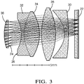
Figure 3 schematically illustrates selected features of another example embodiment of a camera assembly. -
Figure 1 schematically illustrates acamera assembly 20. Asensor 22 is configured to detect radiation and provide an output that may be processed using known techniques for generating an image. Thesensor 22 may be configured for detecting radiation in the visible light spectrum, for example. Given this description, those skilled in the art will be able to select from among commercially available sensors to meet the needs of their particular situation. - An
infrared cut filter 24 is situated to filter radiation as it approaches thesensor 22. Theinfrared cut filter 24 provides enhanced image quality by reducing the amount of infrared radiation incident on thesensor 22. - The
camera assembly 20 includes a plurality oflens elements infrared cut filter 24 and thesensor 22. One way in which the illustrated example embodiment is different than previous camera arrangements is that theinfrared cut filter 24 is spaced away from the sensor with lens elements between theinfrared cut filter 24 and thesensor 22. Most camera assemblies that include an infrared cut filter position that filter immediately in front of the sensor between the sensor and the lens elements. - One feature of the plurality of lens elements is that they include only two aspherical surfaces for a high performance camera system with 1/3" format sensor at 67lp/mm resolution. Potentially more aspherical surfaces might be needed for camera systems with larger sensor format at higher resolution. The illustrated example includes a
doublet lens element 26 having aconcave lens portion 32 and aconvex lens portion 34. The combination of theconcave lens portion 32 and theconvex lens portion 34 provides color correction. Thelens element 28 in this example is a convex lens and thelens element 30 is a meniscus lens. The particulars of the curvatures of thelens elements - The
camera assembly 20 includes afront lens 36 on an opposite side of theinfrared cut filter 24 from the plurality oflens elements front lens 36 is a plano-convex lens element 36 with the convex surface facing forward and away from thesensor 22. Any radiation that will be detected by thesensor 22 first passes through thefront lens 36, theinfrared cut filter 24 and the plurality oflens elements - The example embodiment of
Figure 1 includes ahousing 40 that contains thelens elements front lens 36 and theinfrared cut filter 24. Thesensor 22 is also at least partially situated within thehousing 40 in this example. One feature of the illustrated example is that it allows for thesensor 22 to be received adjacent a printedcircuit board substrate 42 and thecamera assembly 20 is then secured to thesubstrate 42 using a surface mount technique. The assembly process for a surface mount technique typically requires a component, such as thecamera assembly 20, to be within specified size constraints so that the component and thesubstrate 42 may be properly situated within the machinery used for the reflow portion of the surface mount technique. The position of theinfrared cut filter 24 allows for thecamera assembly 20 to fit within such size constraints. - Referring to
Figure 2 , a total track length (TTL) between a forward-most surface of the front lens 36 (e.g., the convex surface) and thesensor 22 is less than 10mm. In one example embodiment, the TTL is 9.6mm. Having a total track length that is less than 10mm allows for thecamera assembly 20 to be secured to a substrate such as thesubstrate 42 using a surface mount technique. The TTL could not fit within such size constraints if theinfrared cut filter 24 were positioned between thelens element 30 and thesensor 22. That position of theinfrared cut filter 24 would increase a back focal length (BFL). In the illustrated example, the BFL is less than 1.0mm. In one particular example, the BFL is 0.7mm. The dimension of the BFL in the illustrated example contributes to realizing a TTL and overall camera assembly dimension that allows for a surface mount technique to be used. - In the example of
Figure 2 , an aperture width (AW) is approximately 3.2mm and a sensor width (SW) is approximately 6.2mm. One feature of the illustrated example is that it allows for having a larger aperture or smaller F#. In one example, F# is 1.65. Another feature of the illustrated example is that it allows for a lower chief ray angle, which can be less than 15° at the desired total track length. - Another feature of the illustrated example is that it allows for reducing the cost of the
infrared cut filter 24 because of its location within thecamera assembly 20. For example, if theinfrared cut filter 24 were the last element before thesensor 22, a higher grade optic component would be required. With the illustrated arrangement, thelens elements sensor 22 after that radiation has already passed through theinfrared cut filter 24. - By positioning the
infrared cut filter 24 near theaperture stop 38 and having the plurality oflens elements infrared cut filter 24 and thesensor 22, a desired level of optical performance can be realized including only two aspherical surfaces and five lens elements. The overall size of the camera assembly, the total track length, and the back focal length all can be kept within size constraints that allows for thecamera assembly 20 to be included in a surface mount technique assembly process. With a surface mount technique, theentire camera assembly 20 may be preassembled and more readily incorporated onto thesubstrate 42, which increases the quality and reliability of the final product. - Although schematically illustrated in
Figures 1 and 2 as a separate element, theinfrared cut filter 24 may be realized as a coating on the flat surface of thefront lens 36 as shown in the example embodiment ofFigure 3 . Such embodiments may provide additional space savings and reduce the complexity of the assembly by reducing the number of individual components that must be properly aligned within thecamera assembly 20. With either alternative, theinfrared cut filter 24 is located near theaperture stop 38 of thecamera assembly 20. - The size and cost savings provided by the unique configuration of the components of the
camera assembly 20 reduces cost, improves packaging considerations, and increases opportunities for additional advanced driver assistance features on a vehicle that rely upon a camera with good imaging capability. - The preceding description is exemplary rather than limiting in nature. Variations and modifications to the disclosed examples may become apparent to those skilled in the art that do not necessarily depart from the essence of this invention. The scope of legal protection given to this invention can only be determined by studying the following claims.
Claims (15)
- A camera assembly (20), comprising:a sensor (22);an infrared cut filter (24) situated to filter radiation as the radiation approaches the sensor (22); anda plurality of lens elements (26, 28, 30) situated between the sensor (22) and the infrared cut filter (24).
- The camera assembly (20) of claim 1, comprising an aperture stop (38) and whereinthe plurality of lens elements (26, 28, 30) are situated between the aperture stop (38) and the sensor (22); andthe infrared cut filter (24) is situated near the aperture stop (38).
- The camera assembly (20) according to any one of the preceding claims, wherein the plurality of lens elements (26, 28, 30) comprise one doublet lens element (26) including a convex lens portion (34) and a concave lens portion (32), the doublet lens element (26) providing color correction.
- The camera assembly (20) of claim 3, wherein
the doublet lens element (26) is further from the sensor (22) than at least one other of the plurality of lens elements (26, 28, 30). - The camera assembly (20) according to any one of claims 3 to 4, wherein
the plurality of lens elements (26, 28, 30) includes a convex lens and a meniscus lens; and
the convex lens and the meniscus lens are between the doublet element and the sensor (22). - The camera assembly (20) according to any one of the preceding claims, wherein
the infrared cut filter (24) is a flat side of a plano-convex lens element (36);
the flat side faces toward the sensor (22); and
a convex side of the plano-convex lens element (36) faces away from the sensor (22). - The camera assembly (20) of claim 6, wherein the plano-convex lens element (36) is a forward-most lens element (26) of the camera.
- The camera assembly (20) according to any one of the preceding claims, comprising
a housing (40) that supports the infrared cut filter (24) and the plurality of lens elements (26, 28, 30);
a printed circuit board substrate (42); and wherein
the housing (40) and the sensor (22) are secured to the printed circuit board substrate (42) using a surface mount technique. - The camera assembly (20) according to any one of the preceding claims, comprising
a front lens (36); and wherein
the infrared cut filter (24) is situated between a forward most surface of the front lens (36) and the plurality of lens elements (26);
the camera assembly (20) has a total track length between the forward most surface of the front lens (36) and the sensor (22); and
the total track length is less than 10mm. - The camera assembly (20) according to any one of the preceding claims, wherein
one of the plurality of lens elements (26, 28, 30) is closer to the sensor (22) than others of the plurality of lens elements (26); and
a back focal distance between the sensor (22) and the one of the plurality of lens elements (26, 28, 30) is less than 1.0mm. - The camera assembly (20) according to any one of the preceding claims, wherein the plurality of lens elements (26, 28, 30) has only 2 aspherical surfaces.
- The camera assembly (20) according to any one of the preceding claims, wherein the sensor (22) is configured to detect radiation in the visible light spectrum.
- A method of making a camera assembly (20), the method comprising:supporting a plurality of lens elements (26, 28, 30) within a housing (40);positioning a sensor (22) near one end of the housing (40);positioning an infrared cut filter (24) near an opposite end of the housing (40) with the plurality of lens elements (26, 28, 30) between the infrared cut filter (24) and the sensor (22);situating the sensor (22) adjacent a circuit board substrate (42); and securing the sensor (22) and the housing (40) to the circuit board substrate (42) using a surface mount technique.
- The method of claim 13, comprising
positioning a front lens (36) near the infrared cut filter (24) with the infrared cut filter (24) between a forward most surface of the front lens (36) and the plurality of lens elements (26); and wherein
the camera assembly (20) has a total track length between the forward most surface of the front lens (36) and the sensor (22); and
the total track length is less than 10mm. - The method according to any one of the claims 13 to 14, wherein
one of the plurality of lens elements (26, 28, 30) is closer to the sensor (22) than others of the plurality of lens elements (26, 28, 30); and
a back focal distance between the sensor (22) and the one of the plurality of lens elements (30) is less than 1.0mm.
Applications Claiming Priority (1)
| Application Number | Priority Date | Filing Date | Title |
|---|---|---|---|
| US15/084,880 US9798054B1 (en) | 2016-03-30 | 2016-03-30 | Camera assembly for use on a vehicle |
Publications (1)
| Publication Number | Publication Date |
|---|---|
| EP3226052A1 true EP3226052A1 (en) | 2017-10-04 |
Family
ID=58401409
Family Applications (1)
| Application Number | Title | Priority Date | Filing Date |
|---|---|---|---|
| EP17161891.1A Withdrawn EP3226052A1 (en) | 2016-03-30 | 2017-03-20 | Camera assembly for use on a vehicle |
Country Status (3)
| Country | Link |
|---|---|
| US (1) | US9798054B1 (en) |
| EP (1) | EP3226052A1 (en) |
| CN (1) | CN107272304A (en) |
Families Citing this family (5)
| Publication number | Priority date | Publication date | Assignee | Title |
|---|---|---|---|---|
| US20170280034A1 (en) * | 2016-03-23 | 2017-09-28 | Magna Electronics Inc. | Vehicle vision system camera with enhanced imager and lens assembly |
| CN111371970B (en) * | 2018-12-26 | 2022-03-15 | 中芯集成电路(宁波)有限公司 | Packaging method of camera shooting assembly |
| US11394955B2 (en) * | 2020-01-17 | 2022-07-19 | Aptiv Technologies Limited | Optics device for testing cameras useful on vehicles |
| CN111246186A (en) * | 2020-01-21 | 2020-06-05 | 重庆金康新能源汽车有限公司 | Vehicle-mounted camera system and method |
| CN111446305B (en) * | 2020-04-23 | 2025-01-07 | 中国科学院上海技术物理研究所 | A hermetic packaging component structure with integrated lens |
Citations (4)
| Publication number | Priority date | Publication date | Assignee | Title |
|---|---|---|---|---|
| CN102830486A (en) * | 2011-06-13 | 2012-12-19 | 奇景光电股份有限公司 | Micro lens module |
| WO2013063014A2 (en) * | 2011-10-24 | 2013-05-02 | Magna Electronics, Inc. | Vehicular camera and lens assembly and method of manufacturing same |
| US20140209786A1 (en) * | 2011-08-19 | 2014-07-31 | Eigo Sano | Image Pickup Lens And Image Pickup Device |
| US20140233111A1 (en) * | 2013-02-20 | 2014-08-21 | AAC Technologies Pte. Ltd. | Imaging Lens |
Family Cites Families (6)
| Publication number | Priority date | Publication date | Assignee | Title |
|---|---|---|---|---|
| US7199868B2 (en) * | 2004-11-02 | 2007-04-03 | Identix Incorporated | High performance fingerprint imaging system |
| TWI426418B (en) * | 2007-12-25 | 2014-02-11 | 世紀民生科技股份有限公司 | Optical navigation sensor and optical navigation device thereof |
| KR101474351B1 (en) * | 2008-11-28 | 2014-12-18 | 제이에스알 가부시끼가이샤 | Near infra red cut filter, and solid state imaging device and camera module comprising the same |
| TWI425825B (en) * | 2009-12-31 | 2014-02-01 | 勝開科技股份有限公司 | Adjustable focus image sensor package structure |
| US9432633B2 (en) * | 2011-12-28 | 2016-08-30 | Pelco, Inc. | Visual command processing |
| CN104216094B (en) * | 2013-05-31 | 2017-03-15 | 比亚迪股份有限公司 | A kind of optical lens |
-
2016
- 2016-03-30 US US15/084,880 patent/US9798054B1/en active Active
-
2017
- 2017-03-20 EP EP17161891.1A patent/EP3226052A1/en not_active Withdrawn
- 2017-03-29 CN CN201710197091.6A patent/CN107272304A/en active Pending
Patent Citations (4)
| Publication number | Priority date | Publication date | Assignee | Title |
|---|---|---|---|---|
| CN102830486A (en) * | 2011-06-13 | 2012-12-19 | 奇景光电股份有限公司 | Micro lens module |
| US20140209786A1 (en) * | 2011-08-19 | 2014-07-31 | Eigo Sano | Image Pickup Lens And Image Pickup Device |
| WO2013063014A2 (en) * | 2011-10-24 | 2013-05-02 | Magna Electronics, Inc. | Vehicular camera and lens assembly and method of manufacturing same |
| US20140233111A1 (en) * | 2013-02-20 | 2014-08-21 | AAC Technologies Pte. Ltd. | Imaging Lens |
Non-Patent Citations (1)
| Title |
|---|
| "Handbook of optical systems, Aberration theory and correction of optical systems", 2 January 2007, WILEY-VCH, Weinheim, DE, ISBN: 978-3-527-40379-0, article HERBERT GROSS ET AL: "Handbook of Optical Systems, Vol.3: Aberration Theory and Correction of Optical Systems", pages: 377 - 379, XP055258161 * |
Also Published As
| Publication number | Publication date |
|---|---|
| US20170285231A1 (en) | 2017-10-05 |
| US9798054B1 (en) | 2017-10-24 |
| CN107272304A (en) | 2017-10-20 |
Similar Documents
| Publication | Publication Date | Title |
|---|---|---|
| US9798054B1 (en) | Camera assembly for use on a vehicle | |
| US9291797B2 (en) | Lens module | |
| US20170280034A1 (en) | Vehicle vision system camera with enhanced imager and lens assembly | |
| US8212689B2 (en) | Objective, in particular for a driver assistance system | |
| US20150358605A1 (en) | Stereo camera module and method for the production thereof | |
| US11022730B2 (en) | Lens module with improved image quality and electronic device with the same | |
| US7894714B2 (en) | Lens assembly and imaging apparatus | |
| US8023211B2 (en) | Lens assembly and image-taking apparatus | |
| EP3432570B1 (en) | Method of making a camera for use on a vehicle | |
| US9851621B2 (en) | Camera for vehicles, in particular commercial vehicles | |
| US10237456B2 (en) | Vehicle camera assembly process | |
| CN112505875A (en) | Periscopic lens module of mobile terminal and mobile terminal | |
| CN109765674B (en) | Camera device module | |
| US20140055641A1 (en) | System for recognizing surroundings of vehicle | |
| US20140293054A1 (en) | Optical device for a vehicle | |
| US10247939B2 (en) | Lens unit, imaging apparatus, and on-vehicle camera | |
| EP3226539A1 (en) | Multi-purpose camera device for use on a vehicle | |
| US10845674B2 (en) | Ghost reducing device, imaging device including same, ghost reducing method, and imaging optical system | |
| JP2016184081A (en) | Lens unit and camera module | |
| CN105511207B (en) | For can PCB installation camera model can PCB installation lens adapter | |
| JP4270993B2 (en) | Tube for converter lens | |
| JP6805854B2 (en) | In-vehicle shooting device and reflection suppression method | |
| JP5184244B2 (en) | Imaging device | |
| CN219370178U (en) | Shading piece, vehicle-mounted camera and vehicle | |
| CN215187042U (en) | Vehicle-mounted imaging device and vehicle |
Legal Events
| Date | Code | Title | Description |
|---|---|---|---|
| PUAI | Public reference made under article 153(3) epc to a published international application that has entered the european phase |
Free format text: ORIGINAL CODE: 0009012 |
|
| AK | Designated contracting states |
Kind code of ref document: A1 Designated state(s): AL AT BE BG CH CY CZ DE DK EE ES FI FR GB GR HR HU IE IS IT LI LT LU LV MC MK MT NL NO PL PT RO RS SE SI SK SM TR |
|
| AX | Request for extension of the european patent |
Extension state: BA ME |
|
| STAA | Information on the status of an ep patent application or granted ep patent |
Free format text: STATUS: THE APPLICATION IS DEEMED TO BE WITHDRAWN |
|
| 18D | Application deemed to be withdrawn |
Effective date: 20180405 |