EP3226007A1 - A mems accelerometer having high accuracy and low sensitivity to temperature and ageing - Google Patents
A mems accelerometer having high accuracy and low sensitivity to temperature and ageing Download PDFInfo
- Publication number
- EP3226007A1 EP3226007A1 EP16194689.2A EP16194689A EP3226007A1 EP 3226007 A1 EP3226007 A1 EP 3226007A1 EP 16194689 A EP16194689 A EP 16194689A EP 3226007 A1 EP3226007 A1 EP 3226007A1
- Authority
- EP
- European Patent Office
- Prior art keywords
- frequency
- suspended region
- signal
- electrical
- bearing structure
- Prior art date
- Legal status (The legal status is an assumption and is not a legal conclusion. Google has not performed a legal analysis and makes no representation as to the accuracy of the status listed.)
- Granted
Links
Images

Classifications
-
- G—PHYSICS
- G01—MEASURING; TESTING
- G01P—MEASURING LINEAR OR ANGULAR SPEED, ACCELERATION, DECELERATION, OR SHOCK; INDICATING PRESENCE, ABSENCE, OR DIRECTION, OF MOVEMENT
- G01P15/00—Measuring acceleration; Measuring deceleration; Measuring shock, i.e. sudden change of acceleration
- G01P15/02—Measuring acceleration; Measuring deceleration; Measuring shock, i.e. sudden change of acceleration by making use of inertia forces using solid seismic masses
- G01P15/08—Measuring acceleration; Measuring deceleration; Measuring shock, i.e. sudden change of acceleration by making use of inertia forces using solid seismic masses with conversion into electric or magnetic values
-
- B—PERFORMING OPERATIONS; TRANSPORTING
- B81—MICROSTRUCTURAL TECHNOLOGY
- B81B—MICROSTRUCTURAL DEVICES OR SYSTEMS, e.g. MICROMECHANICAL DEVICES
- B81B3/00—Devices comprising flexible or deformable elements, e.g. comprising elastic tongues or membranes
- B81B3/0018—Structures acting upon the moving or flexible element for transforming energy into mechanical movement or vice versa, i.e. actuators, sensors, generators
- B81B3/0021—Transducers for transforming electrical into mechanical energy or vice versa
-
- G—PHYSICS
- G01—MEASURING; TESTING
- G01P—MEASURING LINEAR OR ANGULAR SPEED, ACCELERATION, DECELERATION, OR SHOCK; INDICATING PRESENCE, ABSENCE, OR DIRECTION, OF MOVEMENT
- G01P15/00—Measuring acceleration; Measuring deceleration; Measuring shock, i.e. sudden change of acceleration
- G01P15/02—Measuring acceleration; Measuring deceleration; Measuring shock, i.e. sudden change of acceleration by making use of inertia forces using solid seismic masses
- G01P15/08—Measuring acceleration; Measuring deceleration; Measuring shock, i.e. sudden change of acceleration by making use of inertia forces using solid seismic masses with conversion into electric or magnetic values
- G01P15/0802—Details
-
- G—PHYSICS
- G01—MEASURING; TESTING
- G01P—MEASURING LINEAR OR ANGULAR SPEED, ACCELERATION, DECELERATION, OR SHOCK; INDICATING PRESENCE, ABSENCE, OR DIRECTION, OF MOVEMENT
- G01P15/00—Measuring acceleration; Measuring deceleration; Measuring shock, i.e. sudden change of acceleration
- G01P15/02—Measuring acceleration; Measuring deceleration; Measuring shock, i.e. sudden change of acceleration by making use of inertia forces using solid seismic masses
- G01P15/08—Measuring acceleration; Measuring deceleration; Measuring shock, i.e. sudden change of acceleration by making use of inertia forces using solid seismic masses with conversion into electric or magnetic values
- G01P15/125—Measuring acceleration; Measuring deceleration; Measuring shock, i.e. sudden change of acceleration by making use of inertia forces using solid seismic masses with conversion into electric or magnetic values by capacitive pick-up
-
- B—PERFORMING OPERATIONS; TRANSPORTING
- B81—MICROSTRUCTURAL TECHNOLOGY
- B81B—MICROSTRUCTURAL DEVICES OR SYSTEMS, e.g. MICROMECHANICAL DEVICES
- B81B2201/00—Specific applications of microelectromechanical systems
- B81B2201/02—Sensors
- B81B2201/0228—Inertial sensors
- B81B2201/0235—Accelerometers
-
- B—PERFORMING OPERATIONS; TRANSPORTING
- B81—MICROSTRUCTURAL TECHNOLOGY
- B81B—MICROSTRUCTURAL DEVICES OR SYSTEMS, e.g. MICROMECHANICAL DEVICES
- B81B2203/00—Basic microelectromechanical structures
- B81B2203/01—Suspended structures, i.e. structures allowing a movement
- B81B2203/0181—See-saws
-
- B—PERFORMING OPERATIONS; TRANSPORTING
- B81—MICROSTRUCTURAL TECHNOLOGY
- B81B—MICROSTRUCTURAL DEVICES OR SYSTEMS, e.g. MICROMECHANICAL DEVICES
- B81B2203/00—Basic microelectromechanical structures
- B81B2203/04—Electrodes
-
- G—PHYSICS
- G01—MEASURING; TESTING
- G01P—MEASURING LINEAR OR ANGULAR SPEED, ACCELERATION, DECELERATION, OR SHOCK; INDICATING PRESENCE, ABSENCE, OR DIRECTION, OF MOVEMENT
- G01P15/00—Measuring acceleration; Measuring deceleration; Measuring shock, i.e. sudden change of acceleration
- G01P15/02—Measuring acceleration; Measuring deceleration; Measuring shock, i.e. sudden change of acceleration by making use of inertia forces using solid seismic masses
- G01P15/08—Measuring acceleration; Measuring deceleration; Measuring shock, i.e. sudden change of acceleration by making use of inertia forces using solid seismic masses with conversion into electric or magnetic values
- G01P2015/0805—Measuring acceleration; Measuring deceleration; Measuring shock, i.e. sudden change of acceleration by making use of inertia forces using solid seismic masses with conversion into electric or magnetic values being provided with a particular type of spring-mass-system for defining the displacement of a seismic mass due to an external acceleration
- G01P2015/0808—Measuring acceleration; Measuring deceleration; Measuring shock, i.e. sudden change of acceleration by making use of inertia forces using solid seismic masses with conversion into electric or magnetic values being provided with a particular type of spring-mass-system for defining the displacement of a seismic mass due to an external acceleration for defining in-plane movement of the mass, i.e. movement of the mass in the plane of the substrate
- G01P2015/0811—Measuring acceleration; Measuring deceleration; Measuring shock, i.e. sudden change of acceleration by making use of inertia forces using solid seismic masses with conversion into electric or magnetic values being provided with a particular type of spring-mass-system for defining the displacement of a seismic mass due to an external acceleration for defining in-plane movement of the mass, i.e. movement of the mass in the plane of the substrate for one single degree of freedom of movement of the mass
- G01P2015/0814—Measuring acceleration; Measuring deceleration; Measuring shock, i.e. sudden change of acceleration by making use of inertia forces using solid seismic masses with conversion into electric or magnetic values being provided with a particular type of spring-mass-system for defining the displacement of a seismic mass due to an external acceleration for defining in-plane movement of the mass, i.e. movement of the mass in the plane of the substrate for one single degree of freedom of movement of the mass for translational movement of the mass, e.g. shuttle type
-
- G—PHYSICS
- G01—MEASURING; TESTING
- G01P—MEASURING LINEAR OR ANGULAR SPEED, ACCELERATION, DECELERATION, OR SHOCK; INDICATING PRESENCE, ABSENCE, OR DIRECTION, OF MOVEMENT
- G01P15/00—Measuring acceleration; Measuring deceleration; Measuring shock, i.e. sudden change of acceleration
- G01P15/02—Measuring acceleration; Measuring deceleration; Measuring shock, i.e. sudden change of acceleration by making use of inertia forces using solid seismic masses
- G01P15/08—Measuring acceleration; Measuring deceleration; Measuring shock, i.e. sudden change of acceleration by making use of inertia forces using solid seismic masses with conversion into electric or magnetic values
- G01P2015/0805—Measuring acceleration; Measuring deceleration; Measuring shock, i.e. sudden change of acceleration by making use of inertia forces using solid seismic masses with conversion into electric or magnetic values being provided with a particular type of spring-mass-system for defining the displacement of a seismic mass due to an external acceleration
- G01P2015/0822—Measuring acceleration; Measuring deceleration; Measuring shock, i.e. sudden change of acceleration by making use of inertia forces using solid seismic masses with conversion into electric or magnetic values being provided with a particular type of spring-mass-system for defining the displacement of a seismic mass due to an external acceleration for defining out-of-plane movement of the mass
- G01P2015/0825—Measuring acceleration; Measuring deceleration; Measuring shock, i.e. sudden change of acceleration by making use of inertia forces using solid seismic masses with conversion into electric or magnetic values being provided with a particular type of spring-mass-system for defining the displacement of a seismic mass due to an external acceleration for defining out-of-plane movement of the mass for one single degree of freedom of movement of the mass
- G01P2015/0831—Measuring acceleration; Measuring deceleration; Measuring shock, i.e. sudden change of acceleration by making use of inertia forces using solid seismic masses with conversion into electric or magnetic values being provided with a particular type of spring-mass-system for defining the displacement of a seismic mass due to an external acceleration for defining out-of-plane movement of the mass for one single degree of freedom of movement of the mass the mass being of the paddle type having the pivot axis between the longitudinal ends of the mass, e.g. see-saw configuration
-
- G—PHYSICS
- G01—MEASURING; TESTING
- G01P—MEASURING LINEAR OR ANGULAR SPEED, ACCELERATION, DECELERATION, OR SHOCK; INDICATING PRESENCE, ABSENCE, OR DIRECTION, OF MOVEMENT
- G01P15/00—Measuring acceleration; Measuring deceleration; Measuring shock, i.e. sudden change of acceleration
- G01P15/02—Measuring acceleration; Measuring deceleration; Measuring shock, i.e. sudden change of acceleration by making use of inertia forces using solid seismic masses
- G01P15/08—Measuring acceleration; Measuring deceleration; Measuring shock, i.e. sudden change of acceleration by making use of inertia forces using solid seismic masses with conversion into electric or magnetic values
- G01P2015/0862—Measuring acceleration; Measuring deceleration; Measuring shock, i.e. sudden change of acceleration by making use of inertia forces using solid seismic masses with conversion into electric or magnetic values being provided with particular means being integrated into a MEMS accelerometer structure for providing particular additional functionalities to those of a spring mass system
Definitions
- the present invention relates to an accelerometric sensor obtained using MEMS (Micro-Electro-Mechanical Systems) technology that has high accuracy and low sensitivity to temperature and ageing.
- MEMS Micro-Electro-Mechanical Systems
- an accelerometric sensor or accelerometer is an inertial sensor that converts an acceleration into an electrical signal.
- An accelerometric sensor obtained using MEMS technology is basically made up of a mobile structure and a detection system, which is coupled to the mobile structure and generates a corresponding electrical signal (for example, a capacitive variation), which is, in turn, is supplied to a processing interface.
- the patent US 8,671,756 describes a microelectromechanical sensing structure for a MEMS resonant biaxial accelerometer.
- the microelectromechanical sensing structure includes an inertial mass anchored to a substrate by means of elastic elements in such a way as to be suspended over the substrate.
- the elastic elements enable inertial sensing movements of the inertial mass along a first sensing axis and a second sensing axis that belong to a plane of main extension of the inertial mass, in response to respective linear external accelerations.
- the microelectromechanical sensing structure comprises at least one first resonant element and one second resonant element, which have respective longitudinal extensions along the first and second sensing axes, and are mechanically coupled to the inertial mass via a corresponding elastic element, in such a way as to be subjected to a respective axial stress, when the inertial mass is displaced, respectively, along the first and second sensing axes.
- the accelerometers can be used in numerous applications; for example, they can form corresponding inclinometers.
- the electrical signal supplied by the accelerometer it is required for the electrical signal supplied by the accelerometer to be particularly precise and accurate.
- ZGO zero-gravity offset
- accelerometers are subjected to undesirable phenomena, such as, for example, temperature variations, ageing, mechanical stresses, etc.
- undesirable phenomena such as, for example, temperature variations, ageing, mechanical stresses, etc.
- the aforesaid undesirable phenomena cause onset of spurious components within the electrical signals generated by the accelerometers, i.e., components not correlated with the accelerations to which the accelerometers are subjected, with consequent reduction of the accuracy of the accelerometers.
- the aim of the present invention is to provide an accelerometric sensor, which, as compared to the prior art, has a low sensitivity to temperature and ageing.
- an accelerometric sensor and a method for detecting an accelerometric signal are provided, as defined in claims 1 and 14.
- FIG. 1 is a schematic illustration of the structure of an embodiment of an accelerometer 1 that is designed to detect accelerations, manufactured in an integrated way using MEMS technology.
- the accelerometer 1 is configured to detect an acceleration, indicated by the arrow a ext , directed parallel to an axis X of an orthogonal reference system XYZ.
- the accelerometer 1 is formed in a die of semiconductor material and comprises a suspended region 2 and a bearing structure 3, fixed with respect to the die and hence referred to hereinafter as "fixed region 3"; visible in Figure 1 is only a portion of the fixed region 3, which surrounds the suspended region 2.
- the fixed region 3 delimits a main cavity C, extending inside which is the suspended region 2.
- the suspended region 2 comprises a first portion 5a, which will be referred to in what follows as “main body 5a”, and a second portion 5b, which will be referred to in what follows as “control element 5b".
- the main body 5a and the control element 5b are made of semiconductor material (for example, monocrystalline or polycrystalline silicon). More in particular, the main body 5a and the control element 5b are provided in one and the same layer of semiconductor material and are monolithic with, and hence fixed with respect to, one another.
- the main body 5a is constrained to the fixed region 3 via a first anchorage 4 and a second anchorage 6, as well as via a first elastic suspension element 8 and a second elastic suspension element 9, which are also referred to as "first and second springs" and function as translational springs.
- the main body 5a has a rectangular shape in top plan view (in the plane XY), with sides parallel to the axes X and Y; moreover, the main body 5a has a thickness (measured parallel to the axis Z, perpendicular to the plane of the drawing) smaller than the dimensions in the directions parallel to the axes X and Y.
- the plane XY is parallel to a surface of main extension of the main body 5a of the suspended region 2.
- the thickness of the main body 5a of the suspended region 2 may be in the region of 20-30 ⁇ m; in the example illustrated in Figure 1 , the control element 5b has the same thickness as the main body 5a and is coplanar with the latter.
- Each of the first and second anchorages 4, 6 is substantially formed by a column, which extends in the direction perpendicular to the plane of the drawing (i.e., parallel to the axis Z), starting from a substrate (not visible), which forms part of the fixed region 3 and which extends underneath the suspended region 2.
- the first and second anchorages 4, 6 are set on opposite sides with respect to the main body 5a of the suspended region 2 and at a distance from the latter (in particular, without any loss of generality, on the minor sides of the rectangle formed in top plan view by the main body 5a of the suspended region 2).
- first and second anchorages 4, 6 are arranged specularly with respect to the main body 5a of the suspended region 2, along an axis (not shown) parallel to the axis X, which in top plan view divides in an imaginary way the main body 5a into two equal and specular portions.
- the first spring 8 has a first end and a second end, which are mechanically fixed, respectively, to the first anchorage 4 and to a corresponding portion of the main body 5a of the suspended region 2.
- the respective first and second ends of the second spring 9 are mechanically fixed, respectively, to the second anchorage 6 and to a corresponding portion of the main body 5a of the suspended region 2.
- the first and second springs 8, 9 are arranged in a symmetrical way on opposite sides of the main body 5a of the suspended region 2.
- first and second springs 8, 9 are elastically deformable, for example, under the action of the acceleration a ext so as to enable the suspended region 2 to translate with respect to the fixed region 3, parallel to the axis X and in both senses.
- the first and second springs 8, 9 are coplanar with the suspended region 2 and have the same thickness as the latter.
- the main body 5a of the suspended region 2 forms a number of (in particular, four) secondary cavities CS, which are the same as one another.
- Embodiments are, however, possible where there is present, for example, just one secondary cavity CS, or in any case a number of secondary cavities CS other than four.
- Each secondary cavity CS has the shape of a parallelepiped, and hence in top plan view has the shape of a rectangle, and moreover extends throughout the thickness of the main body 5b. Extending within each secondary cavity CS is a corresponding pair of conductive plates, which are referred to hereinafter as "first and second fixed plates 12, 14".
- the first fixed plates 12 of the secondary cavities CS are the same as one another and are made of conductive material (for example, doped semiconductor material, such as doped silicon).
- the second fixed plates 14 of the secondary cavities CS are the same as one another and are made of conductive material (for example, doped semiconductor material, such as doped silicon).
- first and second fixed plates 12, 14 are the same as one another, are arranged facing one another, and are fixed to the aforementioned substrate of the fixed region 3 so as to be fixed with respect to the latter; moreover, the first and second fixed plates 12, 14 are parallel to and face, respectively, a first side wall 16 and a second side wall 18 of the secondary cavity CS, which are opposite to one another and parallel to the plane YZ.
- each of the first and second fixed plates 12, 14 may have one and the same height (measured along the axis Z); moreover, the first and second fixed plates 12, 14 may be arranged vertically (i.e., parallel to the axis Z) in such a way that the respective geometrical centres are located at one and the same height.
- the first fixed plate 12 and the first side wall 16 form a first sensing capacitor, the capacitance of which depends, among other things, upon the distance between the first fixed plate 12 and the first side wall 16.
- the second fixed plate 14 and the second side wall 18 form a second sensing capacitor, the capacitance of which depends, among other things, upon the distance between the second fixed plate 14 and the second side wall 18. It follows that the capacitance of the first and second sensing capacitors depend upon the position of the suspended region 2 with respect to the fixed region 3, and hence upon the acceleration a ext to which the accelerometer 1 is subjected, which will be referred to in what follows as "external acceleration a ext ".
- the capacitive variations of the first and second sensing capacitors of each secondary cavity CS are used for measuring the external acceleration a ext , via a capacitance-to-voltage converter interface.
- the first and second sensing capacitors of the secondary cavities CS hence form a sensing assembly of a capacitive type.
- the accelerometer 1 further comprises an electrode 20, which will be referred to in what follows as "modulation electrode 20".
- the modulation electrode 20 is fixed to the substrate of the fixed region 3 and has to a first approximation a U shape, in top plan view. Furthermore, once again in top plan view, the modulation electrode 20 faces, at a distance, one of the major sides of the main body 5a.
- the modulation electrode 20 includes a first lateral portion 22 and a second lateral portion 24 and a transverse portion 26, which are monolithic with respect to one another and are fixed with respect to the fixed region 3. Furthermore, the modulation electrode 20 is made of a conductive material, such as, for example, doped semiconductor material (e.g., doped silicon).
- a conductive material such as, for example, doped semiconductor material (e.g., doped silicon).
- each of the transverse portion 26 and the first and second lateral portions 22, 24 is substantially parallelepipedal in shape. Furthermore, in the example illustrated in Figures 1 and 2 , the transverse portion 26 and the first and second lateral portions 22, 24 are coplanar and have one and the same thickness, the latter being the same, to a first approximation, as the thickness of the suspended region 2.
- the modulation electrode 20 may be fixed to the substrate of the fixed region 3 in such a way that, if the maximum and minimum heights of the suspended region 2 are referred to, respectively, as “maximum height” and “minimum height", to a first approximation also the first and second lateral portions 22, 24 extend between the maximum height and the minimum height.
- first and second lateral portions 22, 24 are arranged specularly with respect to a plane H, which is parallel to the plane YZ and represents, in resting conditions, a plane of symmetry of the accelerometer 1.
- Each of the first and second lateral portions 22, 24 has a pair of side walls parallel to the plane H.
- the transverse portion 26 has ends connected to the first and second lateral portions 22, 24 so as to connect them together; without any loss of generality, in resting conditions, the transverse portion 26 is traversed by the plane H, which divides it into two sub-portions that are the same as one another and specular.
- control element 5b in the example illustrated in Figures 1 and 2 it has the shape of a parallelepiped and extends from the main body 5a towards the modulation electrode 20.
- the control element 5b extends from the side of the main body 5a that the modulation electrode 20 faces, in the direction of the latter, in a way such as to be arranged between the first and second lateral portions 22, 24 of the modulation electrode 20.
- the control element 5b extends at least in part within a cavity CC delimited by the modulation electrode 20, which will be referred to in what follows as "control cavity CC".
- control element 5b is delimited laterally by a pair of walls, which are opposite to one another and parallel to the plane YZ and will be referred to in what follows as “first and second suspended walls S e1 , S e2 ", these walls facing the first and second lateral portions 22, 24, respectively, of the modulation electrode 20.
- first and second lateral portions 22, 24 of the modulation electrode 20 are delimited, respectively, by a first fixed wall S m1 and a second fixed wall S m2 , which face, respectively, the first and second suspended walls S e1 , S e2 , to which they are parallel.
- transverse portion 26 of the modulation electrode 20 is delimited by a further wall S t , which faces the control element 5b and is perpendicular to the first and second fixed walls S m1 , S m2 , with which it is in direct contact.
- first and second fixed walls S m1 , S m2 are equipotential.
- first and second suspended walls S e1 , S e2 are equipotential.
- first control capacitor 30 the first lateral portion 22 of the modulation electrode 20 and the control element 5b form a capacitor 30, which will be referred to hereinafter as "first control capacitor 30".
- second control capacitor 32 the second lateral portion 24 of the modulation electrode 20 and the control element 5b form a further capacitor 32, which will be referred to hereinafter as "second control capacitor 32".
- the capacitance of the first control capacitor 30 depends upon the area of lateral overlapping (i.e., parallel to the axis X) of the first fixed wall S m1 and of the first suspended wall S e1 .
- this area is equal to L ov ⁇ t ov , where L ov is, as shown in Figure 2 , the length (measured parallel to the axis Y) of the portion of first suspended wall S e1 that laterally overlaps the first fixed wall S m1 , while t ov is the height (measured parallel to the axis Z) of the aforesaid portion and to a first approximation is equal to the thickness of the suspended region 2.
- the capacitance of the first control capacitor 30 depends upon the distance between the first fixed wall S m1 and the first suspended wall S e1 , which can be expressed as (go + x), where go is the distance between the aforesaid walls in resting conditions, while x is the variation of the aforesaid distance with respect to the value of g 0 .
- the quantity x will be referred to also as "deviation”.
- the capacitance of the second control capacitor 32 depends upon the area of lateral overlapping of the second fixed wall S m2 and of the second suspended wall S e2 , which is once again equal to L ov ⁇ t ov . Furthermore, the capacitance of the second control capacitor 32 depends upon the distance between the second fixed wall S m2 and the second suspended wall S e2 , which can be expressed as (g 0- x). Consequently, without any loss of generality, in resting conditions, the control element 5b is equidistant from the first and the second fixed wall S m1 , S m2 , and the first and second control capacitors 30, 32 have substantially one and the same capacitance.
- the modulation electrode 20 is set at a voltage V m
- the suspended region 2 and hence also the control element 5b, is set at a voltage V rotor . Consequently, on the control element 5b, and hence more in general on the suspended region 2, two electrostatic forces are exerted in one and the same direction, but in opposite senses, these forces being denoted in what follows as F el,1 and F el,2 .
- the voltage V m applied to the modulation electrode 20 can be written as the sum of a constant component V dc and a variable component ⁇ V ⁇ sen( ⁇ m t), where t, ⁇ m , and ⁇ V are, respectively, the time and the pulsation of the variable (oscillating) component and the corresponding amplitude.
- V m t V dc + ⁇ V ⁇ sen ⁇ m t
- Eq. (6) can be rewritten as: F el , tot ⁇ k e 1 , 0 + ⁇ k ⁇ sen ⁇ m t ⁇ x where: k el , 0 ⁇ 2 ⁇ 0 L ov t ov g 0 3 ⁇ V dc 2 ⁇ k ⁇ 4 ⁇ 0 L ov t ov g 0 3 ⁇ V dc ⁇ ⁇ V
- x t x off T , stresses , etc . + a ext t ⁇ el 2 ⁇ a ext t ⁇ el 2 ⁇ ⁇ k k ⁇ k el , 0 ⁇ sen ⁇ m t
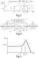
- the first term of the right-hand member (x off ) is a first contribution to the deviation x, which includes the undesired effects such as, for example, temperature (T), mechanical stresses, etc. Since these undesired effects are very slowly variable in time, the first contribution may be considered as a so-called d.c. contribution, as shown in Figure 3 , where it is designated by 37.
- the second term of the right-hand member of Eq. (15) represents a second contribution to the deviation x, which depends upon the external acceleration a ext , but not upon the pulsation ⁇ m .
- the third term of the right-hand member of Eq. (15) represents a third contribution to the deviation x, which depends both upon the external acceleration a ext and upon the pulsation ⁇ m ; in particular, in the frequency domain, the third contribution is translated in frequency with respect to the first and second contributions in a way proportional to the frequency f m , as shown qualitatively in Figure 3 .
- Figure 4 shows a processing circuit 44 set downstream of the accelerometer 1, which is represented schematically as a block subjected to the external acceleration a ext .
- Figure 4 shows a voltage generator 46, which generates the voltage V m and is connected to the accelerometer 1 in such a way that, in use, the modulation electrode 20 is set at the voltage V m .
- the processing circuit 44 comprises a capacitance-to-voltage converter block 48, a high-pass filter 50, which implements, for example, the transfer function 41 shown in Figure 3 , and a demodulator 52.
- the accelerometer 1 is formed in a first die D1
- the voltage generator 46, the capacitance-to-voltage converter 48, the high-pass filter 50, and the demodulator 52 are provided in a second die, for example, as ASIC.
- Embodiments are in any case possible where the accelerometer 1, the voltage generator 46, and the processing circuit 44 are all formed in one and the same die.
- the capacitance-to-voltage converter circuit 48 is a connection interface, which is formed, for example, by a charge amplifier of a type in itself known, which is electrically connected to the pairs of sensing capacitors formed in the aforementioned secondary cavities CS of the accelerometer 1 so as to receive a capacitive-variation signal s ⁇ C generated by these sensing capacitors, in a way in itself known.
- the capacitive-variation signal s ⁇ C depends upon the deviation x, and hence indicates the value of the latter, since, considering any of the secondary cavities CS, the distance between the respective first fixed plate 12 and the respective first side wall 16 and the distance between the second fixed plate 14 and the second side wall 18 depend upon the deviation x.
- the capacitive-variation signal s ⁇ C includes respective components, which correspond to the aforementioned first, second, and third contributions of deviation x.
- the capacitance-to-voltage converter circuit 48 generates at output a signal to be filtered s v , which is formed, for example, by a voltage that depends upon the capacitance of the sensing capacitors formed in the secondary cavities CS, and hence also indicates the value of the deviation x.
- the signal to be filtered s v includes respective components, which correspond to the aforementioned first, second, and third contributions of the deviation x.
- the signal to be filtered s v is then filtered by the high-pass filter 50, which generates a filtered signal s f that depends upon the aforementioned third contribution to the deviation x, but not upon the first and second contributions to the deviation x.
- the high-pass filter 50 filters the components of the signal to be filtered s v that correspond to the first and second contributions of the deviation x.
- the filtered signal s f is supplied on a first input of the demodulator 52, which is of a type in itself known and may include a multiplier and a low-pass filter (not illustrated). Moreover, the voltage generator 46 supplies the voltage V m on a second input of the demodulator 52, in such a way that the latter supplies an output signal s out , which once again indicates the value of the deviation x, but has a lower frequency than the filtered signal s f . For instance, the output signal s out may be in base band.
- the capacitive-variation signal s ⁇ C is converted into the signal to be filtered s v by the capacitance-to-voltage converter 48, is filtered by the high-pass filter 50, and is then demodulated by the demodulator 52.
- the output signal s out is a function, among other things, of the external acceleration a ext , of V dc and ⁇ V, but not of the pulsation ⁇ m .
- the output signal s out may be supplied to an output stage 58, which is formed, for example, by an external device configured to generate an acceleration signal s aext indicating the external acceleration a ext , on the basis of the output signal s out .
- the acceleration signal s aext may be of an analog or digital type; in this latter case, the output stage 58 may include an A/D converter (not illustrated).
- the output stage 58 it is, for example, possible to carry out operations of calibration in the presence of known accelerations (for example, the acceleration of gravity) so as to determine, for each known acceleration, the corresponding value of the output signal s out .
- the frequency response H(s) indicates, as a function of the frequency of an external mechanical driving force in sinusoidal regime, the values of amplitude of the corresponding sinusoidal oscillation to which the suspended region 2 is subjected, with respect to the position assumed in resting conditions.
- the frequency response H(s) has a peak at a frequency value equal to the aforementioned mechanical resonance frequency f mech .
- the frequency f m belongs to a frequency range that includes the mechanical resonance frequency f mech and is such that the modulus of H( ⁇ m ) assumes values at least equal, for example, to
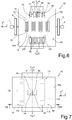
- Figure 6 represents a embodiment of the accelerometer (here designated by 60), which is described with reference to the sole differences with respect to the embodiment shown in Figure 1 . Moreover, elements already present in the embodiment illustrated in Figure 1 are designated by the same references, except where otherwise specified.
- the suspended region (here designated by 62) once again includes the main body, here designated by 65a, but does not comprise the control element.
- the main body 65a forms, in addition to the secondary cavities CS, a plurality of control cavities, here designated by CC'.
- the control cavities CC' are the same as one another, have the shape of a parallelepiped, and extend throughout the thickness of the main body 65a; in top plan view, each control cavity CC' hence has the shape of a rectangle.
- each set extends on opposite sides with respect to the set of the secondary cavities CS, which are arranged evenly spaced apart along an axis parallel to the axis X; moreover, in each set, the control cavities CC' are also arranged evenly spaced apart along a respective axis parallel to the axis X, for example, with a spacing smaller than the spacing of the secondary cavities CS.
- Embodiments are, however, possible where each of the two sets is formed by a different number of control cavities CC' and/or just one set is present. Furthermore, it is possible for the main body 65a to form a single control cavity CC', even though in this case the accelerometer 60 is no longer symmetrical.
- the accelerometer 60 further comprises a plurality of modulation electrodes, here designated by 68, which are the same as one another, are made of conductive material (for example, doped semiconductor material), and have the shape of parallelepipeds.
- the modulation electrodes 68 are set at the voltage V m
- the suspended region 62 is set at the voltage V rotor .
- each modulation electrode 68 extends in a corresponding control cavity CC' and, as already described with reference to the embodiment illustrated in Figure 1 , is fixed to the substrate of the fixed region 3.
- each modulation electrode 68 is delimited by a first side wall 70 and a second side wall 72, which are opposite to one another and parallel to the plane YZ, and face at a distance, respectively, a first side wall 76 and a second side wall 78 of the corresponding control cavity CC', which are also opposite to one another and parallel to the plane YZ.
- the first side wall 70 of the modulation electrode 68 forms, together with the first side wall 76 of the corresponding control cavity CC', a corresponding capacitor 80, which will be referred to once again as “first control capacitor”, since it performs the same function as the first control capacitor 30 of the embodiment illustrated in Figure 1 .
- the second side wall 72 of the modulation electrode 68 forms, together with the second side wall 78 of the corresponding control cavity CC', a corresponding capacitor 82, which will be referred to once again as "second control capacitor”, since it performs the same function as the second control capacitor 32 of the embodiment illustrated in Figure 1 .
- the first and second side walls 70, 72 of the modulation electrode 68 are both at the voltage V m ; the first and second side walls 76, 78 of the corresponding control cavity CC' are both at the voltage V rotor .
- the distance between the first side wall 70 of the modulation electrode 68 and the first side wall 76 of the corresponding control cavity CC' and the distance between the second side wall 72 of the modulation electrode 68 and the second side wall 78 of the corresponding control cavity CC' are the same as one another, and the first and second control capacitors 80, 82 have capacitances that are the same as one another.
- the accelerometer 60 there can be applied the equations mentioned with reference to the embodiment illustrated in Figures 1 and 2 , after prior adaptation to the change in geometrical conditions.
- the accelerometer 60 envisages a plurality of modulation electrodes 68, and hence a plurality of first control capacitors 80, which are electrically coupled to corresponding second control capacitors 82; moreover, each modulation electrode 68 is surrounded by the suspended region 62.
- operation of the accelerometer 60 is similar to that of the accelerometer 1.
- FIGs 7-8 show a further embodiment of the accelerometer, here designated by 90.
- the accelerometer 90 is designed to detect an external acceleration directed parallel to the axis Z.
- Figure 8 illustrates also the first anchorage 94.
- the accelerometer 90 comprises the suspended region, here designated by 92, which is constrained to the fixed region 3 (not visible in Figure 7 ) via the first anchorage, here designated by 94, as well as via the first and second springs, here designated by 98 and 99, which are of the type that is deformable in rotation; i.e., they operate in torsion.
- the suspended region 92 includes the main body, here designated by 95a, but not the control element.
- the anchorage 94 extends in an opening 100 in the suspended region 92, which extends throughout the thickness of the latter.
- the first and second springs 98, 99 are coplanar to the suspended region 92 and extend through the opening 100, parallel to the axis Y, between the first anchorage 94 and two respective opposite points of a portion of main body 95a that delimits the opening 100.
- the first anchorage 94 and the first and second springs 98, 99 are here shaped so as to enable rotation of the suspended region 92 only about an axis of rotation O, parallel to the axis Y. In practice, in the course of rotation, portions of the suspended region 92 exit from the plane of the sheet.
- rotation is due to the fact that the suspended region 92 is asymmetrical with respect to the axis of rotation O.
- the axis of rotation O is eccentric with respect to the barycenter (not shown) of the suspended region 92; i.e., the axis of rotation O is shifted with respect to the barycenter by a non-zero arm, which is parallel to the axis Y.
- the accelerometer 90 further comprises a first fixed plate and a second fixed plate, here designated by 102 and 104, which are fixed to the substrate of the fixed region 3 and are arranged parallel to the plane XY. Since the suspended region 92 overlies the first and second fixed plates 102, 104, it forms with the latter, respectively, a first sensing capacitor and a second sensing capacitor, the capacitances of which depend upon the angle ⁇ , which indicates the degree of rotation of the suspended region 92 with respect to the position assumed in resting conditions, the latter position being parallel to the plane XY. Without any loss of generality, in resting conditions, the first and second sensing capacitors may have approximately one and the same capacitance. Once again without any loss of generality, in top plan view the first and second fixed plates 102, 104 may have the shape of rectangles elongated in a direction parallel to the axis Y and arranged specularly with respect to the first anchorage 94.
- the accelerometer 90 further comprises a first pair of electrodes 110 and a second pair of electrodes 112, these pairs being the same as one another and being arranged specularly with respect to an imaginary axis parallel to the axis X and passing, in top plan view, through the first anchorage 94.
- a first pair of electrodes 110 and a second pair of electrodes 112 these pairs being the same as one another and being arranged specularly with respect to an imaginary axis parallel to the axis X and passing, in top plan view, through the first anchorage 94.
- the second pair of electrodes 112 is absent; moreover, since the first and second pairs of electrodes 110, 112 are the same as one another, in what follows only the first pair of electrodes 110 will be described.
- the first pair of electrodes 110 comprises a first modulation electrode 114 and a second modulation electrode 116, which, without any loss of generality, are the same as one another and are formed by corresponding plates parallel to the plane XY, fixed to the substrate of the fixed region 3.
- the first and second modulation electrodes 114, 116 are equidistant from the axis of rotation O.
- the suspended region 92 is arranged on top of, and at a distance from, the first and second modulation electrodes 114 and 116 and forms with the latter, respectively, the first and second control capacitors, here designated by 130 and 132.
- the values of capacitance of the first and second control capacitors 130, 132 also depend upon the angle ⁇ . Without any loss generality, in resting conditions, the first and second control capacitors 130, 132 may have one and the same value of capacitance.
- the first and second pairs of electrodes 110, 112 are set at the voltage V m
- the suspended region 92 is set at the voltage V rotor . Consequently, on the suspended region 92 there are exerted the two electrostatic forces F el,1 and F el,2 , which cause application to the suspended region 92 of two corresponding couples that tend to cause the suspended region 92 to turn in opposite directions.
- J ⁇ + b ⁇ + k ⁇ m ⁇ a ext ⁇ r + F el , tot ⁇ r el
- J is the rotational moment of inertia of the suspended region 92
- b is the damping (caused by viscous friction)
- k is the elastic stiffness of the system formed by the suspended region 92 and by the first and second springs 98, 99
- r is the aforementioned mechanical arm, i.e., the arm defined by the barycenter of the suspended region 92 and by the axis of rotation O
- r el is the electrostatic arm, which is equal to the distance from the axis of rotation O of the centre of either of the first and second modulation electrodes 114, 116.
- ⁇ t m ⁇ a ext t k ⁇ k el , 0 1 ⁇ ⁇ k k ⁇ k el , 0 ⁇ sen ⁇ m t
- the embodiments previously described envisage the presence of at least two control capacitors, each of which has a fixed plate, fixed with respect to the fixed plate of the other control capacitor and to the fixed region, and a mobile plate, fixed with respect to the mobile plate of the other control capacitor and to the suspended region, the capacitances of the two control capacitors varying with opposite sign following upon the (translational or rotational) movement of the suspended region with respect to the fixed region.
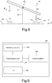
- FIG. 9 shows a block diagram of an electronic device 300, which comprises an accelerometer, such as one of the accelerometers 1, 60, 90, referred to herein, as packaged device 200.
- the accelerometer may be used, for example, for detecting vibrations, for determining the orientation of the electronic device 300, or for recognising free-fall conditions.
- the electronic device 300 may be a mobile communication apparatus, such as a cellphone or a personal digital assistant, a portable computer, a photographic-camera or video-camera device, a wearable device, such as a smartwatch, or any other electronic device.
- the electronic device 300 comprises a processing unit 310, which is electrically coupled to the packaged device 200.
- the processing unit 310 includes a control circuitry, formed, for example, by one or more processors, discrete memory and logic, including the output stage 58 illustrated in Figure 4 .
- the processing unit 310 is configured for transmitting and receiving signals to/from the packaged device 200.
- the electronic device 300 may further comprise an input/output device 320, such as a keypad or a display coupled to the processing unit 310.
- the electronic device 300 may moreover comprise a power supply 330, which may be formed by a battery or by components for coupling to an external supply source.
- the accelerometer described enables detection of external accelerations in a very accurate way, thanks to the possibility of eliminating the d.c. components, or in any case low-frequency components, that adversely affect the stability and precision of measurement.
- the present accelerometer can be set in the same cavity as that of a gyroscope, in the case where an apparatus envisages both devices, enabling a reduction of the space occupied.
- the present accelerometer does not require the presence of any driving circuit designed to keep mechanical parts in oscillation, with consequent reduction of the complexity of implementation.
- the shape of the suspended region may be different from the one described, as likewise the number and arrangement of the sensing capacitors, and hence also the shapes and arrangements of the conductive elements that form the corresponding plates.
- the number and shapes of the secondary cavities may be different from what has been described.
- the shape and arrangement of the control element (if present) and the shapes and arrangements of one or more of the modulation electrodes described previously may be different; consequently, also the shapes and arrangements of one or more of the control cavities (if present) may be different from what has been described previously.
- embodiments (not shown) are in any case possible corresponding to embodiments described previously, but where a single control capacitor is present, the first and second plates of which are formed, respectively, by the modulation electrode and by the suspended region.
- a single control capacitor is present, the first and second plates of which are formed, respectively, by the modulation electrode and by the suspended region.
- the voltage V m may even be without any d.c. component, in which case modulation of the stiffness will occur at a frequency that is twice the frequency f m .
- the a.c. component of the voltage V m may be different from a sinusoid, provided that it remains periodic.
- the voltage V m may be formed by a square wave, in which case a so-called chopping technique is implemented.
- the processing circuit 44 and/or the output stage 58 may vary as a function of the time plot of the voltage V m .
Landscapes
- Physics & Mathematics (AREA)
- General Physics & Mathematics (AREA)
- Chemical & Material Sciences (AREA)
- Analytical Chemistry (AREA)
- Engineering & Computer Science (AREA)
- Computer Hardware Design (AREA)
- Microelectronics & Electronic Packaging (AREA)
- Pressure Sensors (AREA)
- Micromachines (AREA)
Abstract
Description
- The present invention relates to an accelerometric sensor obtained using MEMS (Micro-Electro-Mechanical Systems) technology that has high accuracy and low sensitivity to temperature and ageing.
- As is known, an accelerometric sensor or accelerometer is an inertial sensor that converts an acceleration into an electrical signal. An accelerometric sensor obtained using MEMS technology is basically made up of a mobile structure and a detection system, which is coupled to the mobile structure and generates a corresponding electrical signal (for example, a capacitive variation), which is, in turn, is supplied to a processing interface.
- For instance, the
patent US 8,671,756 describes a microelectromechanical sensing structure for a MEMS resonant biaxial accelerometer. The microelectromechanical sensing structure includes an inertial mass anchored to a substrate by means of elastic elements in such a way as to be suspended over the substrate. The elastic elements enable inertial sensing movements of the inertial mass along a first sensing axis and a second sensing axis that belong to a plane of main extension of the inertial mass, in response to respective linear external accelerations. Furthermore, the microelectromechanical sensing structure comprises at least one first resonant element and one second resonant element, which have respective longitudinal extensions along the first and second sensing axes, and are mechanically coupled to the inertial mass via a corresponding elastic element, in such a way as to be subjected to a respective axial stress, when the inertial mass is displaced, respectively, along the first and second sensing axes. - In general, the accelerometers can be used in numerous applications; for example, they can form corresponding inclinometers. However, in numerous applications, it is required for the electrical signal supplied by the accelerometer to be particularly precise and accurate. In this connection, in some applications it is required for the so-called ZGO (zero-gravity offset) stability to be less than 0.00981 m/s2.
- In greater detail, accelerometers are subjected to undesirable phenomena, such as, for example, temperature variations, ageing, mechanical stresses, etc. The aforesaid undesirable phenomena cause onset of spurious components within the electrical signals generated by the accelerometers, i.e., components not correlated with the accelerations to which the accelerometers are subjected, with consequent reduction of the accuracy of the accelerometers.
- The aim of the present invention is to provide an accelerometric sensor, which, as compared to the prior art, has a low sensitivity to temperature and ageing.
- According to the present invention, an accelerometric sensor and a method for detecting an accelerometric signal are provided, as defined in
claims - For a better understanding of the present invention, preferred embodiments thereof are now described, purely by way of non-limiting example, with reference to the attached drawings, wherein:
-
Figure 1 shows a schematic top plan view of an embodiment of the present accelerometer; -
Figure 2 shows a schematic top plan view of a portion of the embodiment illustrated inFigure 1 ; -
Figure 3 is a schematic illustration of the frequency spectrum of a displacement signal and the corresponding spectral contributions, as well as a frequency response of a high-pass filter; -
Figure 4 shows a block diagram of a circuitry for processing a signal supplied by the present accelerometer; -
Figure 5 is a schematic illustration of the frequency spectrum of a portion of a displacement signal and the spectrum of a frequency response of a mechanical system formed by the present accelerometer; -
Figures 6 and 7 are schematic top plan views of further embodiments of the present accelerometer; -
Figure 8 is a schematic cross-sectional view of a portion of the embodiment illustrated inFigure 7 , taken along the plane of section VIII-VIII ofFigure 7 ; and -
Figure 9 shows a block diagram of an electronic apparatus including the present accelerometer. -
Figure 1 is a schematic illustration of the structure of an embodiment of anaccelerometer 1 that is designed to detect accelerations, manufactured in an integrated way using MEMS technology. In the example illustrated, theaccelerometer 1 is configured to detect an acceleration, indicated by the arrow aext, directed parallel to an axis X of an orthogonal reference system XYZ. - The
accelerometer 1 is formed in a die of semiconductor material and comprises a suspendedregion 2 and abearing structure 3, fixed with respect to the die and hence referred to hereinafter as "fixed region 3"; visible inFigure 1 is only a portion of thefixed region 3, which surrounds the suspendedregion 2. - The
fixed region 3 delimits a main cavity C, extending inside which is the suspendedregion 2. - The suspended
region 2 comprises afirst portion 5a, which will be referred to in what follows as "main body 5a", and asecond portion 5b, which will be referred to in what follows as "control element 5b". Themain body 5a and thecontrol element 5b are made of semiconductor material (for example, monocrystalline or polycrystalline silicon). More in particular, themain body 5a and thecontrol element 5b are provided in one and the same layer of semiconductor material and are monolithic with, and hence fixed with respect to, one another. - The
main body 5a is constrained to thefixed region 3 via afirst anchorage 4 and asecond anchorage 6, as well as via a firstelastic suspension element 8 and a secondelastic suspension element 9, which are also referred to as "first and second springs" and function as translational springs. - In greater detail, in the example illustrated in
Figure 1 , themain body 5a has a rectangular shape in top plan view (in the plane XY), with sides parallel to the axes X and Y; moreover, themain body 5a has a thickness (measured parallel to the axis Z, perpendicular to the plane of the drawing) smaller than the dimensions in the directions parallel to the axes X and Y. In other words, the plane XY is parallel to a surface of main extension of themain body 5a of the suspendedregion 2. For instance, the thickness of themain body 5a of the suspendedregion 2 may be in the region of 20-30 µm; in the example illustrated inFigure 1 , thecontrol element 5b has the same thickness as themain body 5a and is coplanar with the latter. - Each of the first and
second anchorages fixed region 3 and which extends underneath thesuspended region 2. In addition, in top plan view, the first andsecond anchorages main body 5a of the suspendedregion 2 and at a distance from the latter (in particular, without any loss of generality, on the minor sides of the rectangle formed in top plan view by themain body 5a of the suspended region 2). In practice, the first andsecond anchorages main body 5a of the suspendedregion 2, along an axis (not shown) parallel to the axis X, which in top plan view divides in an imaginary way themain body 5a into two equal and specular portions. - The
first spring 8 has a first end and a second end, which are mechanically fixed, respectively, to thefirst anchorage 4 and to a corresponding portion of themain body 5a of the suspendedregion 2. The respective first and second ends of thesecond spring 9 are mechanically fixed, respectively, to thesecond anchorage 6 and to a corresponding portion of themain body 5a of the suspendedregion 2. In practice, in resting conditions (described in greater detail hereinafter), the first andsecond springs main body 5a of the suspendedregion 2. Furthermore, the first andsecond springs region 2 to translate with respect to thefixed region 3, parallel to the axis X and in both senses. Without any loss of generality, the first andsecond springs region 2 and have the same thickness as the latter. - In the example illustrated in
Figure 1 , themain body 5a of the suspendedregion 2 forms a number of (in particular, four) secondary cavities CS, which are the same as one another. Embodiments (not illustrated) are, however, possible where there is present, for example, just one secondary cavity CS, or in any case a number of secondary cavities CS other than four. - Each secondary cavity CS has the shape of a parallelepiped, and hence in top plan view has the shape of a rectangle, and moreover extends throughout the thickness of the
main body 5b. Extending within each secondary cavity CS is a corresponding pair of conductive plates, which are referred to hereinafter as "first and secondfixed plates - In the example illustrated in
Figure 1 , the firstfixed plates 12 of the secondary cavities CS are the same as one another and are made of conductive material (for example, doped semiconductor material, such as doped silicon). Likewise, the secondfixed plates 14 of the secondary cavities CS are the same as one another and are made of conductive material (for example, doped semiconductor material, such as doped silicon). - In greater detail, in the example illustrated in
Figure 1 , given a secondary cavity CS, the respective first and secondfixed plates fixed region 3 so as to be fixed with respect to the latter; moreover, the first and secondfixed plates first side wall 16 and asecond side wall 18 of the secondary cavity CS, which are opposite to one another and parallel to the plane YZ. In even greater detail, each of the first and secondfixed plates fixed plates - From an electrical standpoint, the first
fixed plate 12 and thefirst side wall 16 form a first sensing capacitor, the capacitance of which depends, among other things, upon the distance between the firstfixed plate 12 and thefirst side wall 16. Likewise, the secondfixed plate 14 and thesecond side wall 18 form a second sensing capacitor, the capacitance of which depends, among other things, upon the distance between the secondfixed plate 14 and thesecond side wall 18. It follows that the capacitance of the first and second sensing capacitors depend upon the position of the suspendedregion 2 with respect to thefixed region 3, and hence upon the acceleration aext to which theaccelerometer 1 is subjected, which will be referred to in what follows as "external acceleration aext". - As described in greater detail hereinafter, the capacitive variations of the first and second sensing capacitors of each secondary cavity CS are used for measuring the external acceleration aext, via a capacitance-to-voltage converter interface. The first and second sensing capacitors of the secondary cavities CS hence form a sensing assembly of a capacitive type.
- Once again with reference to
Figure 1 , theaccelerometer 1 further comprises anelectrode 20, which will be referred to in what follows as "modulation electrode 20". Themodulation electrode 20 is fixed to the substrate of thefixed region 3 and has to a first approximation a U shape, in top plan view. Furthermore, once again in top plan view, themodulation electrode 20 faces, at a distance, one of the major sides of themain body 5a. - As shown in greater detail in
Figure 2 , in the example illustrated inFigure 1 themodulation electrode 20 includes a firstlateral portion 22 and a secondlateral portion 24 and atransverse portion 26, which are monolithic with respect to one another and are fixed with respect to thefixed region 3. Furthermore, themodulation electrode 20 is made of a conductive material, such as, for example, doped semiconductor material (e.g., doped silicon). - Each of the
transverse portion 26 and the first and secondlateral portions Figures 1 and 2 , thetransverse portion 26 and the first and secondlateral portions region 2. Without any loss of generality, themodulation electrode 20 may be fixed to the substrate of thefixed region 3 in such a way that, if the maximum and minimum heights of the suspendedregion 2 are referred to, respectively, as "maximum height" and "minimum height", to a first approximation also the first and secondlateral portions - In greater detail, the first and second
lateral portions accelerometer 1. Each of the first and secondlateral portions - The
transverse portion 26 has ends connected to the first and secondlateral portions transverse portion 26 is traversed by the plane H, which divides it into two sub-portions that are the same as one another and specular. As regards the aforementioned resting conditions, they envisage that the accelerometer is not subjected to any external acceleration (i.e., aext = 0) and themodulation electrode 20 and the suspendedregion 2 are set at one and the same voltage. - Once again with reference to the
control element 5b, in the example illustrated inFigures 1 and 2 it has the shape of a parallelepiped and extends from themain body 5a towards themodulation electrode 20. In particular, in top plan view, thecontrol element 5b extends from the side of themain body 5a that themodulation electrode 20 faces, in the direction of the latter, in a way such as to be arranged between the first and secondlateral portions modulation electrode 20. In other words, thecontrol element 5b extends at least in part within a cavity CC delimited by themodulation electrode 20, which will be referred to in what follows as "control cavity CC". - In greater detail, the
control element 5b is delimited laterally by a pair of walls, which are opposite to one another and parallel to the plane YZ and will be referred to in what follows as "first and second suspended walls Se1, Se2", these walls facing the first and secondlateral portions modulation electrode 20. In turn, the first and secondlateral portions modulation electrode 20 are delimited, respectively, by a first fixed wall Sm1 and a second fixed wall Sm2, which face, respectively, the first and second suspended walls Se1, Se2, to which they are parallel. In addition, thetransverse portion 26 of themodulation electrode 20 is delimited by a further wall St, which faces thecontrol element 5b and is perpendicular to the first and second fixed walls Sm1, Sm2, with which it is in direct contact. - In use, as described in greater detail hereinafter, the first and second fixed walls Sm1, Sm2 are equipotential. Likewise, the first and second suspended walls Se1, Se2 are equipotential.
- In practice, the first
lateral portion 22 of themodulation electrode 20 and thecontrol element 5b form acapacitor 30, which will be referred to hereinafter as "first control capacitor 30". Likewise, the secondlateral portion 24 of themodulation electrode 20 and thecontrol element 5b form afurther capacitor 32, which will be referred to hereinafter as "second control capacitor 32". - The capacitance of the
first control capacitor 30 depends upon the area of lateral overlapping (i.e., parallel to the axis X) of the first fixed wall Sm1 and of the first suspended wall Se1. In this connection, it may be noted how this area is equal to Lov·tov, where Lov is, as shown inFigure 2 , the length (measured parallel to the axis Y) of the portion of first suspended wall Se1 that laterally overlaps the first fixed wall Sm1, while tov is the height (measured parallel to the axis Z) of the aforesaid portion and to a first approximation is equal to the thickness of the suspendedregion 2. Furthermore, the capacitance of thefirst control capacitor 30 depends upon the distance between the first fixed wall Sm1 and the first suspended wall Se1, which can be expressed as (go + x), where go is the distance between the aforesaid walls in resting conditions, while x is the variation of the aforesaid distance with respect to the value of g0. In what follows, the quantity x will be referred to also as "deviation". - The capacitance of the
second control capacitor 32 depends upon the area of lateral overlapping of the second fixed wall Sm2 and of the second suspended wall Se2, which is once again equal to Lov·tov. Furthermore, the capacitance of thesecond control capacitor 32 depends upon the distance between the second fixed wall Sm2 and the second suspended wall Se2, which can be expressed as (g0-x). Consequently, without any loss of generality, in resting conditions, thecontrol element 5b is equidistant from the first and the second fixed wall Sm1, Sm2, and the first andsecond control capacitors - In use, the
modulation electrode 20 is set at a voltage Vm, whereas the suspendedregion 2, and hence also thecontrol element 5b, is set at a voltage Vrotor. Consequently, on thecontrol element 5b, and hence more in general on the suspendedregion 2, two electrostatic forces are exerted in one and the same direction, but in opposite senses, these forces being denoted in what follows as Fel,1 and Fel,2. In particular, recalling that a capacitor subjected to a voltage ΔVs is subjected to an electrostatic force approximately equal to ½· (ΔC/Δx) ·ΔVs 2 (where ΔC is variation of capacitance of the capacitor following upon a variation equal to Δx of the distance of the respective plates), we have:

- Assuming, Vrotor = 0 and x << g0, i.e., assuming small variations with respect to the resting conditions, it is possible to linearize the expression of the total electrostatic force Fel,tot that acts on the suspended
region 2, which is :
- To a first approximation, the total electrostatic force Fel,tot is hence linearly proportional to the deviation of the suspended
region 2 from the position assumed in resting conditions. Furthermore, the total electrostatic force Fel,tot can be understood as a sort of electrostatic stiffness, since it can be expressed as Fel,tot ≈ kel·x, where:
- The voltage Vm applied to the
modulation electrode 20 can be written as the sum of a constant component Vdc and a variable component ΔV·sen(ωmt), where t, ωm, and ΔV are, respectively, the time and the pulsation of the variable (oscillating) component and the corresponding amplitude. In other words, we have:
- The following relation consequently applies:

- Assuming that Vdc>>ΔV/2, Eq. (6) can be rewritten as:


- This having been said, the equation that describes the motion of the suspended
region 2 can be written as:
region 2; b is the damping (caused by viscous friction); and k is the elastic constant (or stiffness) of the system formed by the suspendedregion 2 and by the first andsecond springs - Eq. (10) can be rewritten, to a first approximation, as:

- In quasi-static approximation, i.e., when the frequency fm = ωm/2π is much lower than the mechanical resonance frequency fmech of the system formed by the suspended
region 2 and the first andsecond springs 
- By linearizing the right-hand member of Eq. (12), i.e., by expanding the right-hand member of Eq. (12) into a first-order series with variable Δk (with respect to which the derivative is computed) and around the point (k-kel,0), we obtain:


- Considering also the undesirable effects, it is thus possible to formulate the following equation:

Figure 3 , where it is designated by 37. The second term of the right-hand member of Eq. (15) represents a second contribution to the deviation x, which depends upon the external acceleration aext, but not upon the pulsation ωm. The third term of the right-hand member of Eq. (15) represents a third contribution to the deviation x, which depends both upon the external acceleration aext and upon the pulsation ωm; in particular, in the frequency domain, the third contribution is translated in frequency with respect to the first and second contributions in a way proportional to the frequency fm, as shown qualitatively inFigure 3 . By way of example, inFigure 3 it has been assumed that the external acceleration aext has a sinusoidal plot with frequency fin, in which case the aforementioned second contribution is formed by a single spectral line (designated by 38) at the frequency fin, whereas the third contribution includes a pair of corresponding spectral lines (designated by 39 and 40) set, respectively, at the frequency fm-fin and at the frequency fm + fin. Furthermore,Figure 3 shows qualitatively thetransfer function 41 of a high-pass filter described hereinafter. - In order to render the
accelerometer 1 insensitive to acoustic vibrations, it is possible to impose fm > 20 kHz, in addition to fmech > 20 kHz. - All this having been said, generation of a signal saext representing the external acceleration aext can be performed as illustrated in
Figure 4 , which shows aprocessing circuit 44 set downstream of theaccelerometer 1, which is represented schematically as a block subjected to the external acceleration aext. In addition,Figure 4 shows avoltage generator 46, which generates the voltage Vm and is connected to theaccelerometer 1 in such a way that, in use, themodulation electrode 20 is set at the voltage Vm. - In the example of embodiment of
Figure 4 , theprocessing circuit 44 comprises a capacitance-to-voltage converter block 48, a high-pass filter 50, which implements, for example, thetransfer function 41 shown inFigure 3 , and ademodulator 52. Without any loss of generality, theaccelerometer 1 is formed in a first die D1, whereas thevoltage generator 46, the capacitance-to-voltage converter 48, the high-pass filter 50, and thedemodulator 52 are provided in a second die, for example, as ASIC. Embodiments (not illustrated) are in any case possible where theaccelerometer 1, thevoltage generator 46, and theprocessing circuit 44 are all formed in one and the same die. - In greater detail, the capacitance-to-
voltage converter circuit 48 is a connection interface, which is formed, for example, by a charge amplifier of a type in itself known, which is electrically connected to the pairs of sensing capacitors formed in the aforementioned secondary cavities CS of theaccelerometer 1 so as to receive a capacitive-variation signal sΔC generated by these sensing capacitors, in a way in itself known. On the basis of what has been described previously, the capacitive-variation signal sΔC depends upon the deviation x, and hence indicates the value of the latter, since, considering any of the secondary cavities CS, the distance between the respective first fixedplate 12 and the respectivefirst side wall 16 and the distance between the second fixedplate 14 and thesecond side wall 18 depend upon the deviation x. In addition, the capacitive-variation signal sΔC includes respective components, which correspond to the aforementioned first, second, and third contributions of deviation x. - The capacitance-to-
voltage converter circuit 48 generates at output a signal to be filtered sv, which is formed, for example, by a voltage that depends upon the capacitance of the sensing capacitors formed in the secondary cavities CS, and hence also indicates the value of the deviation x. In other words, also the signal to be filtered sv includes respective components, which correspond to the aforementioned first, second, and third contributions of the deviation x. - The signal to be filtered sv is then filtered by the high-
pass filter 50, which generates a filtered signal sf that depends upon the aforementioned third contribution to the deviation x, but not upon the first and second contributions to the deviation x. In other words, the high-pass filter 50 filters the components of the signal to be filtered sv that correspond to the first and second contributions of the deviation x. - The filtered signal sf is supplied on a first input of the
demodulator 52, which is of a type in itself known and may include a multiplier and a low-pass filter (not illustrated). Moreover, thevoltage generator 46 supplies the voltage Vm on a second input of thedemodulator 52, in such a way that the latter supplies an output signal sout, which once again indicates the value of the deviation x, but has a lower frequency than the filtered signal sf. For instance, the output signal sout may be in base band. - In practice, the capacitive-variation signal sΔC is converted into the signal to be filtered sv by the capacitance-to-
voltage converter 48, is filtered by the high-pass filter 50, and is then demodulated by thedemodulator 52. The output signal sout is a function, among other things, of the external acceleration aext, of Vdc and ΔV, but not of the pulsation ωm. Furthermore, the output signal sout may be supplied to anoutput stage 58, which is formed, for example, by an external device configured to generate an acceleration signal saext indicating the external acceleration aext, on the basis of the output signal sout. The acceleration signal saext may be of an analog or digital type; in this latter case, theoutput stage 58 may include an A/D converter (not illustrated). In order to configure theoutput stage 58, it is, for example, possible to carry out operations of calibration in the presence of known accelerations (for example, the acceleration of gravity) so as to determine, for each known acceleration, the corresponding value of the output signal sout. - According to a variant illustrated in
Figure 5 , in order to increase the amplitude of the output signal sout, it is possible to exploit the characteristics of the so-called frequency response H(s) of the mechanical system formed by the suspendedregion 2 and by the first andsecond springs region 2 is subjected, with respect to the position assumed in resting conditions. In addition, as represented qualitatively inFigure 5 , the frequency response H(s) has a peak at a frequency value equal to the aforementioned mechanical resonance frequency fmech. - Unlike the embodiment described previously, where it has been assumed that operation is such that the
spectral lines Figure 5 it is assumed to operate closer to the resonance peak of the frequency response H(s). In this case, there are benefits deriving from the dynamic amplification given by the closeness to the resonance conditions. Moreover, downstream of the high-pass filter 50, the filtered signal sf indicates the following quantity:
- From a more quantitative standpoint, it may be imposed that the frequency fm belongs to a frequency range that includes the mechanical resonance frequency fmech and is such that the modulus of H(ωm) assumes values at least equal, for example, to |H(0)| +3 dB.
- Irrespective of the relative arrangement between the frequency fm and the mechanical resonance frequency fmech, embodiments of the type illustrated in
Figure 6 are possible, where for simplicity of illustration the fixedregion 3 is not shown. - In detail,
Figure 6 represents a embodiment of the accelerometer (here designated by 60), which is described with reference to the sole differences with respect to the embodiment shown inFigure 1 . Moreover, elements already present in the embodiment illustrated inFigure 1 are designated by the same references, except where otherwise specified. - In greater detail, the suspended region (here designated by 62) once again includes the main body, here designated by 65a, but does not comprise the control element.
- The
main body 65a forms, in addition to the secondary cavities CS, a plurality of control cavities, here designated by CC'. Purely by way of example, the control cavities CC' are the same as one another, have the shape of a parallelepiped, and extend throughout the thickness of themain body 65a; in top plan view, each control cavity CC' hence has the shape of a rectangle. - More in particular, in the embodiment illustrated in
Figure 6 eight control cavities CC' are present, divided into two sets of four, the two sets being arranged specularly with respect to an imaginary axis parallel to the axis X. In practice, each set extends on opposite sides with respect to the set of the secondary cavities CS, which are arranged evenly spaced apart along an axis parallel to the axis X; moreover, in each set, the control cavities CC' are also arranged evenly spaced apart along a respective axis parallel to the axis X, for example, with a spacing smaller than the spacing of the secondary cavities CS. Embodiments (not shown) are, however, possible where each of the two sets is formed by a different number of control cavities CC' and/or just one set is present. Furthermore, it is possible for themain body 65a to form a single control cavity CC', even though in this case theaccelerometer 60 is no longer symmetrical. - The
accelerometer 60 further comprises a plurality of modulation electrodes, here designated by 68, which are the same as one another, are made of conductive material (for example, doped semiconductor material), and have the shape of parallelepipeds. In use, themodulation electrodes 68 are set at the voltage Vm, whereas the suspendedregion 62 is set at the voltage Vrotor. - Considering any one of the
modulation electrodes 68, it extends in a corresponding control cavity CC' and, as already described with reference to the embodiment illustrated inFigure 1 , is fixed to the substrate of the fixedregion 3. In addition, eachmodulation electrode 68 is delimited by afirst side wall 70 and asecond side wall 72, which are opposite to one another and parallel to the plane YZ, and face at a distance, respectively, afirst side wall 76 and asecond side wall 78 of the corresponding control cavity CC', which are also opposite to one another and parallel to the plane YZ. Consequently, thefirst side wall 70 of themodulation electrode 68 forms, together with thefirst side wall 76 of the corresponding control cavity CC', a correspondingcapacitor 80, which will be referred to once again as "first control capacitor", since it performs the same function as thefirst control capacitor 30 of the embodiment illustrated inFigure 1 . Furthermore, thesecond side wall 72 of themodulation electrode 68 forms, together with thesecond side wall 78 of the corresponding control cavity CC', a correspondingcapacitor 82, which will be referred to once again as "second control capacitor", since it performs the same function as thesecond control capacitor 32 of the embodiment illustrated inFigure 1 . In addition, in use, the first andsecond side walls modulation electrode 68 are both at the voltage Vm; the first andsecond side walls - Without any loss of generality, in resting conditions, the distance between the
first side wall 70 of themodulation electrode 68 and thefirst side wall 76 of the corresponding control cavity CC' and the distance between thesecond side wall 72 of themodulation electrode 68 and thesecond side wall 78 of the corresponding control cavity CC' are the same as one another, and the first andsecond control capacitors accelerometer 60 there can be applied the equations mentioned with reference to the embodiment illustrated inFigures 1 and 2 , after prior adaptation to the change in geometrical conditions. - In practice, the
accelerometer 60 envisages a plurality ofmodulation electrodes 68, and hence a plurality offirst control capacitors 80, which are electrically coupled to correspondingsecond control capacitors 82; moreover, eachmodulation electrode 68 is surrounded by the suspendedregion 62. However, operation of theaccelerometer 60 is similar to that of theaccelerometer 1. -
Figures 7-8 show a further embodiment of the accelerometer, here designated by 90. According to this embodiment, theaccelerometer 90 is designed to detect an external acceleration directed parallel to the axis Z. For greater clarity,Figure 8 illustrates also thefirst anchorage 94. - In detail, the
accelerometer 90 comprises the suspended region, here designated by 92, which is constrained to the fixed region 3 (not visible inFigure 7 ) via the first anchorage, here designated by 94, as well as via the first and second springs, here designated by 98 and 99, which are of the type that is deformable in rotation; i.e., they operate in torsion. - In greater detail, the suspended
region 92 includes the main body, here designated by 95a, but not the control element. - The
anchorage 94 extends in anopening 100 in the suspendedregion 92, which extends throughout the thickness of the latter. The first andsecond springs region 92 and extend through theopening 100, parallel to the axis Y, between thefirst anchorage 94 and two respective opposite points of a portion ofmain body 95a that delimits theopening 100. In a way in itself known, thefirst anchorage 94 and the first andsecond springs region 92 only about an axis of rotation O, parallel to the axis Y. In practice, in the course of rotation, portions of the suspendedregion 92 exit from the plane of the sheet. In this connection, rotation is due to the fact that the suspendedregion 92 is asymmetrical with respect to the axis of rotation O. In particular, the axis of rotation O is eccentric with respect to the barycenter (not shown) of the suspendedregion 92; i.e., the axis of rotation O is shifted with respect to the barycenter by a non-zero arm, which is parallel to the axis Y. - The
accelerometer 90 further comprises a first fixed plate and a second fixed plate, here designated by 102 and 104, which are fixed to the substrate of the fixedregion 3 and are arranged parallel to the plane XY. Since the suspendedregion 92 overlies the first and secondfixed plates region 92 with respect to the position assumed in resting conditions, the latter position being parallel to the plane XY. Without any loss of generality, in resting conditions, the first and second sensing capacitors may have approximately one and the same capacitance. Once again without any loss of generality, in top plan view the first and secondfixed plates first anchorage 94. - The
accelerometer 90 further comprises a first pair ofelectrodes 110 and a second pair ofelectrodes 112, these pairs being the same as one another and being arranged specularly with respect to an imaginary axis parallel to the axis X and passing, in top plan view, through thefirst anchorage 94. Embodiments are, however, possible where the second pair ofelectrodes 112 is absent; moreover, since the first and second pairs ofelectrodes electrodes 110 will be described. - In detail, the first pair of
electrodes 110 comprises afirst modulation electrode 114 and asecond modulation electrode 116, which, without any loss of generality, are the same as one another and are formed by corresponding plates parallel to the plane XY, fixed to the substrate of the fixedregion 3. In top plan view, the first andsecond modulation electrodes - The suspended
region 92 is arranged on top of, and at a distance from, the first andsecond modulation electrodes second control capacitors second control capacitors - In use, the first and second pairs of
electrodes region 92 is set at the voltage Vrotor. Consequently, on the suspendedregion 92 there are exerted the two electrostatic forces Fel,1 and Fel,2, which cause application to the suspendedregion 92 of two corresponding couples that tend to cause the suspendedregion 92 to turn in opposite directions. - It may hence be shown that the following equations apply:

region 92; b is the damping (caused by viscous friction); and k is the elastic stiffness of the system formed by the suspendedregion 92 and by the first andsecond springs region 92 and by the axis of rotation O; rel is the electrostatic arm, which is equal to the distance from the axis of rotation O of the centre of either of the first andsecond modulation electrodes - This having been said, it may be shown that the following relation applies:

- It follows that operation of the
accelerometer 90 is equivalent to what has been described with reference to theaccelerometer 1. - In practice, the embodiments previously described envisage the presence of at least two control capacitors, each of which has a fixed plate, fixed with respect to the fixed plate of the other control capacitor and to the fixed region, and a mobile plate, fixed with respect to the mobile plate of the other control capacitor and to the suspended region, the capacitances of the two control capacitors varying with opposite sign following upon the (translational or rotational) movement of the suspended region with respect to the fixed region.
-
Figure 9 shows a block diagram of anelectronic device 300, which comprises an accelerometer, such as one of theaccelerometers device 200. The accelerometer may be used, for example, for detecting vibrations, for determining the orientation of theelectronic device 300, or for recognising free-fall conditions. - The
electronic device 300 may be a mobile communication apparatus, such as a cellphone or a personal digital assistant, a portable computer, a photographic-camera or video-camera device, a wearable device, such as a smartwatch, or any other electronic device. Theelectronic device 300 comprises aprocessing unit 310, which is electrically coupled to the packageddevice 200. Theprocessing unit 310 includes a control circuitry, formed, for example, by one or more processors, discrete memory and logic, including theoutput stage 58 illustrated inFigure 4 . Theprocessing unit 310 is configured for transmitting and receiving signals to/from the packageddevice 200. Theelectronic device 300 may further comprise an input/output device 320, such as a keypad or a display coupled to theprocessing unit 310. Theelectronic device 300 may moreover comprise apower supply 330, which may be formed by a battery or by components for coupling to an external supply source. - The accelerometer described enables detection of external accelerations in a very accurate way, thanks to the possibility of eliminating the d.c. components, or in any case low-frequency components, that adversely affect the stability and precision of measurement.
- In addition, the present accelerometer can be set in the same cavity as that of a gyroscope, in the case where an apparatus envisages both devices, enabling a reduction of the space occupied. In addition, the present accelerometer does not require the presence of any driving circuit designed to keep mechanical parts in oscillation, with consequent reduction of the complexity of implementation.
- Finally, it is clear that modifications and variations may be made to the accelerometer described and illustrated herein, without thereby departing from the sphere of protection of the present invention, as defined in the annexed claims.
- For instance, the shape of the suspended region may be different from the one described, as likewise the number and arrangement of the sensing capacitors, and hence also the shapes and arrangements of the conductive elements that form the corresponding plates. For instance, as mentioned previously, the number and shapes of the secondary cavities may be different from what has been described. Likewise, also the shape and arrangement of the control element (if present) and the shapes and arrangements of one or more of the modulation electrodes described previously may be different; consequently, also the shapes and arrangements of one or more of the control cavities (if present) may be different from what has been described previously.
- In addition, even though the embodiments previously described envisage substantially the presence of at least two control capacitors, and hence the presence of two pairs of surfaces (plates), the surfaces of each pair facing one another, embodiments (not shown) are in any case possible corresponding to embodiments described previously, but where a single control capacitor is present, the first and second plates of which are formed, respectively, by the modulation electrode and by the suspended region. For instance, with reference to the embodiment that corresponds to the embodiment illustrated in
Figures 1 and 2 , it differs from the latter because the secondlateral portion 24 of themodulation electrode 20 is absent. Consequently, we find Fel,tot = Fel,1, with consequent modification of the equations presented previously. Once again purely by way of example, with reference to the embodiment that corresponds to the embodiment illustrated inFigure 7 and8 , it differs from the latter because the second pair ofelectrodes 112 and thesecond modulation electrode 116 are absent. Once again, even though in the embodiments previously described the at least two control capacitors have plates that are two by two equipotential, embodiments are possible where this condition is not respected, even though this may lead to an increase in the complexity of the mathematical formulas presented previously. Furthermore, even though the embodiments described previously envisage that, between the four plates of the at least two control capacitors, at least two of these four plates are formed by one and the same component of the accelerometer (for example, thecontrol element 5b), embodiments are possible (not shown) where each plate is formed by a corresponding component of the accelerometer. - As regards the voltage Vm, it may even be without any d.c. component, in which case modulation of the stiffness will occur at a frequency that is twice the frequency fm. In this connection, irrespective of the possible presence of the d.c. component, the a.c. component of the voltage Vm may be different from a sinusoid, provided that it remains periodic. For instance, the voltage Vm may be formed by a square wave, in which case a so-called chopping technique is implemented. In general, the
processing circuit 44 and/or theoutput stage 58 may vary as a function of the time plot of the voltage Vm.
Claims (17)
- A MEMS accelerometric sensor, comprising:- a bearing structure (3);- a suspended region (2; 62; 92) of semiconductor material, mobile with respect to the bearing structure;- at least one first modulation electrode (20; 68; 114), which is fixed to the bearing structure and is configured to be biased, in use, with an electrical modulation signal including at least one periodic component having a first frequency;- at least one first variable capacitor (30; 80; 130), formed by said suspended region and by said first modulation electrode, in such a way that the suspended region is subjected to a first electrostatic force that depends upon said electrical modulation signal; and- a sensing assembly (12, 14, 16, 18, 5a; 12, 14, 16, 18, 65a; 102, 104, 95a) configured to generate, when the accelerometric sensor is subjected to an acceleration, an electrical sensing signal, which indicates the position of the suspended region with respect to the bearing structure and includes a frequency-modulated component, which is a function of said acceleration and of said first frequency.
- The accelerometric sensor according to claim 1, further comprising:- at least one second variable capacitor (32; 82; 132), which is formed by said suspended region (2; 62; 92) and by said first modulation electrode (20; 68; 114), or else is formed by said suspended region and by a second modulation electrode (116), which is fixed to the bearing structure (3) and is configured to be biased with said electrical modulation signal;and wherein the suspended region is subjected, in use, to a second electrostatic force that depends upon said electrical modulation signal, said first and second variable capacitors being configured in such a way that the respective capacitances vary as a function of the movement of the suspended region with opposite signs.
- The accelerometric sensor according to claim 2, wherein said first modulation electrode (20) forms a first fixed surface (Sm1) and a second fixed surface (Sm1,) parallel to one another; and wherein the suspended region (2) comprises a main body (5a) and an elongated element (5b), which projects towards the outside of the main body so as to extend between the first and second fixed surfaces, said elongated element forming a first mobile surface (Se1) and a second mobile surface (Se2), which face the first and second fixed surfaces, respectively.
- The accelerometric sensor according to claim 2, wherein the suspended region (62) delimits at least one cavity (CC'); and wherein said first modulation electrode (68) extends in said cavity (CC') and forms said second variable capacitor (82).
- The accelerometric sensor according to claim 3 or claim 4, which forms an in-plane acceleration sensor (1; 60), wherein the suspended region (2; 62) is anchored to the bearing structure (3) by means of elastic suspension elements (8, 9) configured so as to enable a translation of the suspended region with respect to the bearing structure, along an axis of translation (X).
- The accelerometric sensor according to claim 2, which forms an out-of-plane acceleration sensor (90) and comprises said second modulation electrode (116), which forms said second variable capacitor (32; 82; 132); and wherein the suspended region (92) is set overlying said first and second modulation electrodes (114, 116) and is anchored to the bearing structure (3) by means of elastic suspension elements (98, 99) configured so as to enable rotation of the suspended region about an axis of rotation, which is parallel to a surface of main extension of the suspended region.
- The accelerometric sensor according to any one of the preceding claims, said sensor further comprising a generator (46) configured to generate said electrical modulation signal and for biasing said first modulation electrode (20; 68; 114).
- The accelerometric sensor according to claim 7, when depending upon claim 5 or claim 6, wherein the suspended region (2; 62; 92) and the elastic suspension elements (8, 9; 98, 99) form a mechanical system, the frequency response of which has a peak at a second frequency; and wherein said first frequency is comprised in the frequency range such that the modulus of said frequency response is at least equal to the d.c. value of the modulus of said frequency response, increased by 3 dB.
- The accelerometric sensor according to claim 7 or claim 8, further comprising a processing circuit (44) including said generator (46), and:- a conversion interface (48) coupled to the sensing assembly (12, 14, 16, 18, 5a; 12, 14, 16, 18, 65a; 102, 104, 95a) and configured to generate, on the basis of the electrical sensing signal, an electrical signal to be filtered, which comprises a number of respective components, one of said respective components being a function of said frequency-modulated component;- a filter (50) coupled to an output of the conversion interface and configured to filter a d.c. component of the electrical signal to be filtered; and- a demodulator (52) coupled to an output of the filter and configured to generate an output signal that indicates said acceleration and is at a frequency lower than the frequency of said frequency-modulated component.
- The accelerometric sensor according to claim 9, wherein the suspended region (2; 62; 92) and the bearing structure (3) are formed in a first plate (D1) of semiconductor material, and the processing circuit (44) is formed in a second plate (D2) of semiconductor material.
- The accelerometric sensor according to claim 9, wherein the suspended region (2; 62; 92), the bearing structure (3), and the processing circuit (44) are formed in a first plate (D1) of semiconductor material.
- The accelerometric sensor according to any one of the preceding claims, wherein said sensing assembly (12, 14, 16, 18, 5a; 12, 14, 16, 18, 65a; 102, 104, 95a) is of a capacitive type; and wherein said electrical sensing signal is a capacitive-variation signal.
- A portable electronic device comprising an accelerometric sensor (200) according to any one of the preceding claims and a processing unit (310) electrically coupled to the accelerometric sensor.
- A method for detecting an acceleration using a MEMS accelerometric sensor including:- a bearing structure (3);- a suspended region (2; 62; 92) made of semiconductor material, mobile with respect to the bearing structure;- at least one first modulation electrode (20; 68; 114), which is fixed to the bearing structure and is configured to be biased, in use, with an electrical modulation signal including at least one periodic component having a first frequency;- at least one first variable capacitor (30; 80; 130), formed by said suspended region and by said first modulation electrode, in such a way that the suspended region is subjected to a first electrostatic force that depends upon said electrical modulation signal; and- a sensing assembly (12, 14, 16, 18, 5a; 12, 14, 16, 18, 65a; 102, 104, 95a) configured to generate, when the accelerometric sensor is subjected to an acceleration, an electrical sensing signal, which indicates the position of the suspended region with respect to the bearing structure and includes a frequency-modulated component, which is a function of said acceleration and of said first frequency;said method comprising the steps of:- biasing said first modulation electrode (20; 68; 114) with said electrical modulation signal so as to generate said first electrostatic force; and- generating said electrical sensing signal.
- The method of detection according to claim 14, further comprising the steps of:- generating, on the basis of the electrical sensing signal, an electrical signal to be filtered, which comprises a number of respective components, one of said respective components being a function of said frequency-modulated component; and- by filtering a d.c. component of the electrical signal to be filtered, generating an electrical signal to be demodulated.
- The method of detection according to claim 15, further comprising the step of generating, starting from the electrical signal to be demodulated, an output signal that indicates said acceleration and is at a frequency lower than the frequency of said frequency-modulated component.
- The method according to any one of laims 14 to 16, wherein said accelerometric sensor forms a mechanical system, the frequency response of which has a peak at a second frequency; and wherein said step of biasing said first modulation electrode (20; 68; 114) comprises generating said electrical modulation signal so that said first frequency is comprised in the frequency range such that the modulus of said frequency response is at least equal to the d.c. value of the modulus of said frequency response, increased by 3 dB.
Priority Applications (1)
| Application Number | Priority Date | Filing Date | Title |
|---|---|---|---|
| EP19160151.7A EP3524984A1 (en) | 2016-03-31 | 2016-10-19 | A mems accelerometric sensor having high accuracy and low sensitivity to temperature and ageing |
Applications Claiming Priority (1)
| Application Number | Priority Date | Filing Date | Title |
|---|---|---|---|
| ITUA2016A002173A ITUA20162173A1 (en) | 2016-03-31 | 2016-03-31 | ACCELEROMETRIC MEMS SENSOR HAVING HIGH ACCURACY AND REDUCED SENSITIVITY TOWARDS TEMPERATURE AND AGING |
Related Child Applications (2)
| Application Number | Title | Priority Date | Filing Date |
|---|---|---|---|
| EP19160151.7A Division-Into EP3524984A1 (en) | 2016-03-31 | 2016-10-19 | A mems accelerometric sensor having high accuracy and low sensitivity to temperature and ageing |
| EP19160151.7A Division EP3524984A1 (en) | 2016-03-31 | 2016-10-19 | A mems accelerometric sensor having high accuracy and low sensitivity to temperature and ageing |
Publications (2)
| Publication Number | Publication Date |
|---|---|
| EP3226007A1 true EP3226007A1 (en) | 2017-10-04 |
| EP3226007B1 EP3226007B1 (en) | 2019-05-29 |
Family
ID=56235945
Family Applications (2)
| Application Number | Title | Priority Date | Filing Date |
|---|---|---|---|
| EP16194689.2A Active EP3226007B1 (en) | 2016-03-31 | 2016-10-19 | A mems accelerometer having high accuracy and low sensitivity to temperature and ageing |
| EP19160151.7A Withdrawn EP3524984A1 (en) | 2016-03-31 | 2016-10-19 | A mems accelerometric sensor having high accuracy and low sensitivity to temperature and ageing |
Family Applications After (1)
| Application Number | Title | Priority Date | Filing Date |
|---|---|---|---|
| EP19160151.7A Withdrawn EP3524984A1 (en) | 2016-03-31 | 2016-10-19 | A mems accelerometric sensor having high accuracy and low sensitivity to temperature and ageing |
Country Status (4)
| Country | Link |
|---|---|
| US (2) | US10591507B2 (en) |
| EP (2) | EP3226007B1 (en) |
| CN (2) | CN206594197U (en) |
| IT (1) | ITUA20162173A1 (en) |
Families Citing this family (3)
| Publication number | Priority date | Publication date | Assignee | Title |
|---|---|---|---|---|
| ITUA20162173A1 (en) * | 2016-03-31 | 2017-10-01 | St Microelectronics Srl | ACCELEROMETRIC MEMS SENSOR HAVING HIGH ACCURACY AND REDUCED SENSITIVITY TOWARDS TEMPERATURE AND AGING |
| CN113884702B (en) * | 2021-10-18 | 2023-09-26 | 兰州空间技术物理研究所 | A design method to improve the consistency of the scale factor of electrostatic suspension accelerometers |
| IT202200003506A1 (en) | 2022-02-24 | 2023-08-24 | St Microelectronics Srl | MICROMECHANICAL DEVICE FOR IMPROVED ACCELERATION MEASUREMENT |
Citations (4)
| Publication number | Priority date | Publication date | Assignee | Title |
|---|---|---|---|---|
| DE102010031214A1 (en) * | 2010-07-12 | 2012-01-12 | Robert Bosch Gmbh | Micromechanical sensor for measuring e.g. acceleration of electronic stability program in motor car, has control unit designed such that seismic mass is continuously subjected with periodically varying force |
| US8671756B2 (en) | 2010-11-26 | 2014-03-18 | Stmicroelectronics S.R.L. | MEMS biaxial resonant accelerometer |
| EP2713169A1 (en) * | 2012-09-28 | 2014-04-02 | Politecnico Di Milano | Integrated resonant structure for the detection of acceleration and angular velocity, and related MEMS sensor device |
| EP2746780A1 (en) * | 2012-12-19 | 2014-06-25 | Northrop Grumman Guidance and Electronics Company, Inc. | Bias reduction in force rebalanced accelerometers |
Family Cites Families (29)
| Publication number | Priority date | Publication date | Assignee | Title |
|---|---|---|---|---|
| DE69413792T2 (en) * | 1994-01-25 | 1999-03-04 | The Charles Stark Draper Laboratory, Inc., Cambridge, Mass. | Micromechanical tuning fork revolution meter with comb-shaped drive elements |
| US5783973A (en) * | 1997-02-24 | 1998-07-21 | The Charles Stark Draper Laboratory, Inc. | Temperature insensitive silicon oscillator and precision voltage reference formed therefrom |
| US6164134A (en) * | 1999-01-29 | 2000-12-26 | Hughes Electronics Corporation | Balanced vibratory gyroscope and amplitude control for same |
| JP2002296292A (en) * | 2001-01-24 | 2002-10-09 | Fujitsu Ltd | Acceleration sensor |
| US6845670B1 (en) * | 2003-07-08 | 2005-01-25 | Freescale Semiconductor, Inc. | Single proof mass, 3 axis MEMS transducer |
| JP4645013B2 (en) * | 2003-10-03 | 2011-03-09 | パナソニック株式会社 | Acceleration sensor and composite sensor using the same |
| CN100498343C (en) * | 2007-07-12 | 2009-06-10 | 中北大学 | Electric tuning resonance differential frequency accelerator |
| US7690254B2 (en) * | 2007-07-26 | 2010-04-06 | Honeywell International Inc. | Sensor with position-independent drive electrodes in multi-layer silicon on insulator substrate |
| US7578190B2 (en) * | 2007-08-03 | 2009-08-25 | Freescale Semiconductor, Inc. | Symmetrical differential capacitive sensor and method of making same |
| US8104346B2 (en) * | 2008-11-10 | 2012-01-31 | Westerngeco L.L.C. | MEMS-based capacitive sensor |
| TW201020548A (en) | 2008-11-18 | 2010-06-01 | Ind Tech Res Inst | Multi-axis capacitive accelerometer |
| IT1392741B1 (en) * | 2008-12-23 | 2012-03-16 | St Microelectronics Rousset | MICROELETTROMECHANICAL GYROSCOPE WITH IMPROVED REJECTION OF ACCELERATION DISORDERS |
| JP5206709B2 (en) * | 2009-03-18 | 2013-06-12 | 株式会社豊田中央研究所 | Device having a movable body |
| DE102009026462B4 (en) * | 2009-05-26 | 2023-03-30 | Robert Bosch Gmbh | accelerometer |
| EP2309241B1 (en) * | 2009-10-07 | 2016-11-30 | ams international AG | MEMS pressure sensor |
| CN102141575A (en) * | 2011-01-04 | 2011-08-03 | 中国地质大学(武汉) | Differential infrared displacement sensing servo acceleration meter |
| DE102011006422B4 (en) * | 2011-03-30 | 2019-02-28 | Robert Bosch Gmbh | Micromechanical component and sensor device |
| US8875578B2 (en) * | 2011-10-26 | 2014-11-04 | Silicon Laboratories Inc. | Electronic damper circuit for MEMS sensors and resonators |
| FI124794B (en) | 2012-06-29 | 2015-01-30 | Murata Manufacturing Co | Improved resonator |
| EP2932192B1 (en) * | 2012-12-12 | 2020-02-05 | The Regents of The University of California | Frequency readout gyroscope |
| US9190937B2 (en) * | 2013-02-06 | 2015-11-17 | Freescale Semiconductor, Inc. | Stiction resistant mems device and method of operation |
| FR3002324B1 (en) * | 2013-02-19 | 2016-01-22 | Sagem Defense Securite | ELECTROSTATIC PENDULUM ACCELEROMETER SENSOR AND METHOD FOR CONTROLLING SAME |
| US9297825B2 (en) * | 2013-03-05 | 2016-03-29 | Analog Devices, Inc. | Tilt mode accelerometer with improved offset and noise performance |
| DE102013208825B4 (en) * | 2013-05-14 | 2021-05-20 | Robert Bosch Gmbh | Microstructure component and method for manufacturing a microstructure component |
| US9476712B2 (en) * | 2013-07-31 | 2016-10-25 | Honeywell International Inc. | MEMS device mechanism enhancement for robust operation through severe shock and acceleration |
| US10877063B2 (en) * | 2015-12-10 | 2020-12-29 | Invensense, Inc. | MEMS sensor with compensation of residual voltage |
| ITUA20162173A1 (en) * | 2016-03-31 | 2017-10-01 | St Microelectronics Srl | ACCELEROMETRIC MEMS SENSOR HAVING HIGH ACCURACY AND REDUCED SENSITIVITY TOWARDS TEMPERATURE AND AGING |
| ITUA20162172A1 (en) * | 2016-03-31 | 2017-10-01 | St Microelectronics Srl | ACCELEROMETRIC SENSOR MADE IN MEMS TECHNOLOGY WITH HIGH ACCURACY AND REDUCED SENSITIVITY TOWARDS TEMPERATURE AND AGING |
| US10033413B2 (en) * | 2016-05-19 | 2018-07-24 | Analog Devices Global | Mixed-mode digital predistortion |
-
2016
- 2016-03-31 IT ITUA2016A002173A patent/ITUA20162173A1/en unknown
- 2016-09-14 US US15/265,111 patent/US10591507B2/en active Active
- 2016-09-30 CN CN201621102333.6U patent/CN206594197U/en active Active
- 2016-09-30 CN CN201610875657.1A patent/CN107271719B/en active Active
- 2016-10-19 EP EP16194689.2A patent/EP3226007B1/en active Active
- 2016-10-19 EP EP19160151.7A patent/EP3524984A1/en not_active Withdrawn
-
2020
- 2020-02-04 US US16/781,963 patent/US11835541B2/en active Active
Patent Citations (4)
| Publication number | Priority date | Publication date | Assignee | Title |
|---|---|---|---|---|
| DE102010031214A1 (en) * | 2010-07-12 | 2012-01-12 | Robert Bosch Gmbh | Micromechanical sensor for measuring e.g. acceleration of electronic stability program in motor car, has control unit designed such that seismic mass is continuously subjected with periodically varying force |
| US8671756B2 (en) | 2010-11-26 | 2014-03-18 | Stmicroelectronics S.R.L. | MEMS biaxial resonant accelerometer |
| EP2713169A1 (en) * | 2012-09-28 | 2014-04-02 | Politecnico Di Milano | Integrated resonant structure for the detection of acceleration and angular velocity, and related MEMS sensor device |
| EP2746780A1 (en) * | 2012-12-19 | 2014-06-25 | Northrop Grumman Guidance and Electronics Company, Inc. | Bias reduction in force rebalanced accelerometers |
Also Published As
| Publication number | Publication date |
|---|---|
| US10591507B2 (en) | 2020-03-17 |
| ITUA20162173A1 (en) | 2017-10-01 |
| CN107271719A (en) | 2017-10-20 |
| CN206594197U (en) | 2017-10-27 |
| US20200174035A1 (en) | 2020-06-04 |
| CN107271719B (en) | 2021-04-16 |
| EP3226007B1 (en) | 2019-05-29 |
| US11835541B2 (en) | 2023-12-05 |
| EP3524984A1 (en) | 2019-08-14 |
| US20170285064A1 (en) | 2017-10-05 |
Similar Documents
| Publication | Publication Date | Title |
|---|---|---|
| US10036764B2 (en) | Bulk acoustic wave accelerometers | |
| Acar et al. | Experimental evaluation and comparative analysis of commercial variable-capacitance MEMS accelerometers | |
| Rao et al. | A high-resolution area-change-based capacitive MEMS tilt sensor | |
| US11408904B2 (en) | Accelerometric sensor in mems technology having high accuracy and low sensitivity to temperature and ageing | |
| US10884020B2 (en) | Accelerometer | |
| US11835541B2 (en) | MEMS accelerometric sensor having high accuracy and low sensitivity to temperature and aging | |
| TWI616656B (en) | A mems sensor and a semiconductor package | |
| US11698388B2 (en) | Micromechanical device with elastic assembly having variable elastic constant | |
| CN110221098A (en) | Silicon micro-resonance type accelerometer and its self-test method | |
| CN100498343C (en) | Electric tuning resonance differential frequency accelerator | |
| Rao et al. | A High-resolution area-change-based capacitive MEMS accelerometer for tilt sensing | |
| RU2692122C1 (en) | Solid-state linear acceleration sensor | |
| US8893563B1 (en) | Differential capacitance torque sensor | |
| RU170862U1 (en) | SENSITIVE SENSOR OF A SHOCK SENSOR | |
| CN221764498U (en) | MEMS device and electronic device | |
| US20240151741A1 (en) | Mems device having improved detection performances | |
| CN112924015B (en) | Low-frequency signal detection system based on phonon frequency comb | |
| RU2657351C1 (en) | Microelectromechanical primary acceleration transducer | |
| Xiao et al. | A double differential torsional MEMS accelerometer with improved temperature robustness | |
| RU2148830C1 (en) | Acceleration meter | |
| Wang et al. | Optimization and analysis of micro capacitive comb accelerometer | |
| Aoyagi et al. | High‐sensitivity surface micromachinable accelerometer using a ferroelectric substrate and its characterization | |
| RU2556334C1 (en) | Sensitive element of microsystem gyroscope |
Legal Events
| Date | Code | Title | Description |
|---|---|---|---|
| PUAI | Public reference made under article 153(3) epc to a published international application that has entered the european phase |
Free format text: ORIGINAL CODE: 0009012 |
|
| STAA | Information on the status of an ep patent application or granted ep patent |
Free format text: STATUS: THE APPLICATION HAS BEEN PUBLISHED |
|
| AK | Designated contracting states |
Kind code of ref document: A1 Designated state(s): AL AT BE BG CH CY CZ DE DK EE ES FI FR GB GR HR HU IE IS IT LI LT LU LV MC MK MT NL NO PL PT RO RS SE SI SK SM TR |
|
| AX | Request for extension of the european patent |
Extension state: BA ME |
|
| STAA | Information on the status of an ep patent application or granted ep patent |
Free format text: STATUS: REQUEST FOR EXAMINATION WAS MADE |
|
| STAA | Information on the status of an ep patent application or granted ep patent |
Free format text: STATUS: EXAMINATION IS IN PROGRESS |
|
| 17P | Request for examination filed |
Effective date: 20180403 |
|
| RBV | Designated contracting states (corrected) |
Designated state(s): AL AT BE BG CH CY CZ DE DK EE ES FI FR GB GR HR HU IE IS IT LI LT LU LV MC MK MT NL NO PL PT RO RS SE SI SK SM TR |
|
| 17Q | First examination report despatched |
Effective date: 20180504 |
|
| GRAP | Despatch of communication of intention to grant a patent |
Free format text: ORIGINAL CODE: EPIDOSNIGR1 |
|
| STAA | Information on the status of an ep patent application or granted ep patent |
Free format text: STATUS: GRANT OF PATENT IS INTENDED |
|
| INTG | Intention to grant announced |
Effective date: 20181219 |
|
| GRAS | Grant fee paid |
Free format text: ORIGINAL CODE: EPIDOSNIGR3 |
|
| GRAA | (expected) grant |
Free format text: ORIGINAL CODE: 0009210 |
|
| STAA | Information on the status of an ep patent application or granted ep patent |
Free format text: STATUS: THE PATENT HAS BEEN GRANTED |
|
| AK | Designated contracting states |
Kind code of ref document: B1 Designated state(s): AL AT BE BG CH CY CZ DE DK EE ES FI FR GB GR HR HU IE IS IT LI LT LU LV MC MK MT NL NO PL PT RO RS SE SI SK SM TR |
|
| REG | Reference to a national code |
Ref country code: GB Ref legal event code: FG4D |
|
| REG | Reference to a national code |
Ref country code: CH Ref legal event code: EP |
|
| REG | Reference to a national code |
Ref country code: AT Ref legal event code: REF Ref document number: 1138590 Country of ref document: AT Kind code of ref document: T Effective date: 20190615 |
|
| REG | Reference to a national code |
Ref country code: DE Ref legal event code: R096 Ref document number: 602016014535 Country of ref document: DE |
|
| REG | Reference to a national code |
Ref country code: IE Ref legal event code: FG4D |
|
| REG | Reference to a national code |
Ref country code: NL Ref legal event code: MP Effective date: 20190529 |
|
| REG | Reference to a national code |
Ref country code: LT Ref legal event code: MG4D |
|
| PG25 | Lapsed in a contracting state [announced via postgrant information from national office to epo] |
Ref country code: HR Free format text: LAPSE BECAUSE OF FAILURE TO SUBMIT A TRANSLATION OF THE DESCRIPTION OR TO PAY THE FEE WITHIN THE PRESCRIBED TIME-LIMIT Effective date: 20190529 Ref country code: SE Free format text: LAPSE BECAUSE OF FAILURE TO SUBMIT A TRANSLATION OF THE DESCRIPTION OR TO PAY THE FEE WITHIN THE PRESCRIBED TIME-LIMIT Effective date: 20190529 Ref country code: LT Free format text: LAPSE BECAUSE OF FAILURE TO SUBMIT A TRANSLATION OF THE DESCRIPTION OR TO PAY THE FEE WITHIN THE PRESCRIBED TIME-LIMIT Effective date: 20190529 Ref country code: ES Free format text: LAPSE BECAUSE OF FAILURE TO SUBMIT A TRANSLATION OF THE DESCRIPTION OR TO PAY THE FEE WITHIN THE PRESCRIBED TIME-LIMIT Effective date: 20190529 Ref country code: PT Free format text: LAPSE BECAUSE OF FAILURE TO SUBMIT A TRANSLATION OF THE DESCRIPTION OR TO PAY THE FEE WITHIN THE PRESCRIBED TIME-LIMIT Effective date: 20190930 Ref country code: NO Free format text: LAPSE BECAUSE OF FAILURE TO SUBMIT A TRANSLATION OF THE DESCRIPTION OR TO PAY THE FEE WITHIN THE PRESCRIBED TIME-LIMIT Effective date: 20190829 Ref country code: AL Free format text: LAPSE BECAUSE OF FAILURE TO SUBMIT A TRANSLATION OF THE DESCRIPTION OR TO PAY THE FEE WITHIN THE PRESCRIBED TIME-LIMIT Effective date: 20190529 Ref country code: FI Free format text: LAPSE BECAUSE OF FAILURE TO SUBMIT A TRANSLATION OF THE DESCRIPTION OR TO PAY THE FEE WITHIN THE PRESCRIBED TIME-LIMIT Effective date: 20190529 |
|
| PG25 | Lapsed in a contracting state [announced via postgrant information from national office to epo] |
Ref country code: BG Free format text: LAPSE BECAUSE OF FAILURE TO SUBMIT A TRANSLATION OF THE DESCRIPTION OR TO PAY THE FEE WITHIN THE PRESCRIBED TIME-LIMIT Effective date: 20190829 Ref country code: RS Free format text: LAPSE BECAUSE OF FAILURE TO SUBMIT A TRANSLATION OF THE DESCRIPTION OR TO PAY THE FEE WITHIN THE PRESCRIBED TIME-LIMIT Effective date: 20190529 Ref country code: LV Free format text: LAPSE BECAUSE OF FAILURE TO SUBMIT A TRANSLATION OF THE DESCRIPTION OR TO PAY THE FEE WITHIN THE PRESCRIBED TIME-LIMIT Effective date: 20190529 Ref country code: GR Free format text: LAPSE BECAUSE OF FAILURE TO SUBMIT A TRANSLATION OF THE DESCRIPTION OR TO PAY THE FEE WITHIN THE PRESCRIBED TIME-LIMIT Effective date: 20190830 |
|
| REG | Reference to a national code |
Ref country code: AT Ref legal event code: MK05 Ref document number: 1138590 Country of ref document: AT Kind code of ref document: T Effective date: 20190529 |
|
| PG25 | Lapsed in a contracting state [announced via postgrant information from national office to epo] |
Ref country code: EE Free format text: LAPSE BECAUSE OF FAILURE TO SUBMIT A TRANSLATION OF THE DESCRIPTION OR TO PAY THE FEE WITHIN THE PRESCRIBED TIME-LIMIT Effective date: 20190529 Ref country code: AT Free format text: LAPSE BECAUSE OF FAILURE TO SUBMIT A TRANSLATION OF THE DESCRIPTION OR TO PAY THE FEE WITHIN THE PRESCRIBED TIME-LIMIT Effective date: 20190529 Ref country code: DK Free format text: LAPSE BECAUSE OF FAILURE TO SUBMIT A TRANSLATION OF THE DESCRIPTION OR TO PAY THE FEE WITHIN THE PRESCRIBED TIME-LIMIT Effective date: 20190529 Ref country code: SK Free format text: LAPSE BECAUSE OF FAILURE TO SUBMIT A TRANSLATION OF THE DESCRIPTION OR TO PAY THE FEE WITHIN THE PRESCRIBED TIME-LIMIT Effective date: 20190529 Ref country code: CZ Free format text: LAPSE BECAUSE OF FAILURE TO SUBMIT A TRANSLATION OF THE DESCRIPTION OR TO PAY THE FEE WITHIN THE PRESCRIBED TIME-LIMIT Effective date: 20190529 Ref country code: NL Free format text: LAPSE BECAUSE OF FAILURE TO SUBMIT A TRANSLATION OF THE DESCRIPTION OR TO PAY THE FEE WITHIN THE PRESCRIBED TIME-LIMIT Effective date: 20190529 Ref country code: RO Free format text: LAPSE BECAUSE OF FAILURE TO SUBMIT A TRANSLATION OF THE DESCRIPTION OR TO PAY THE FEE WITHIN THE PRESCRIBED TIME-LIMIT Effective date: 20190529 |
|
| PG25 | Lapsed in a contracting state [announced via postgrant information from national office to epo] |
Ref country code: IT Free format text: LAPSE BECAUSE OF FAILURE TO SUBMIT A TRANSLATION OF THE DESCRIPTION OR TO PAY THE FEE WITHIN THE PRESCRIBED TIME-LIMIT Effective date: 20190529 Ref country code: SM Free format text: LAPSE BECAUSE OF FAILURE TO SUBMIT A TRANSLATION OF THE DESCRIPTION OR TO PAY THE FEE WITHIN THE PRESCRIBED TIME-LIMIT Effective date: 20190529 |
|
| REG | Reference to a national code |
Ref country code: DE Ref legal event code: R097 Ref document number: 602016014535 Country of ref document: DE |
|
| PG25 | Lapsed in a contracting state [announced via postgrant information from national office to epo] |
Ref country code: TR Free format text: LAPSE BECAUSE OF FAILURE TO SUBMIT A TRANSLATION OF THE DESCRIPTION OR TO PAY THE FEE WITHIN THE PRESCRIBED TIME-LIMIT Effective date: 20190529 |
|
| PLBE | No opposition filed within time limit |
Free format text: ORIGINAL CODE: 0009261 |
|
| STAA | Information on the status of an ep patent application or granted ep patent |
Free format text: STATUS: NO OPPOSITION FILED WITHIN TIME LIMIT |
|
| PG25 | Lapsed in a contracting state [announced via postgrant information from national office to epo] |
Ref country code: PL Free format text: LAPSE BECAUSE OF FAILURE TO SUBMIT A TRANSLATION OF THE DESCRIPTION OR TO PAY THE FEE WITHIN THE PRESCRIBED TIME-LIMIT Effective date: 20190529 |
|
| 26N | No opposition filed |
Effective date: 20200303 |
|
| PG25 | Lapsed in a contracting state [announced via postgrant information from national office to epo] |
Ref country code: SI Free format text: LAPSE BECAUSE OF FAILURE TO SUBMIT A TRANSLATION OF THE DESCRIPTION OR TO PAY THE FEE WITHIN THE PRESCRIBED TIME-LIMIT Effective date: 20190529 Ref country code: MC Free format text: LAPSE BECAUSE OF FAILURE TO SUBMIT A TRANSLATION OF THE DESCRIPTION OR TO PAY THE FEE WITHIN THE PRESCRIBED TIME-LIMIT Effective date: 20190529 |
|
| REG | Reference to a national code |
Ref country code: CH Ref legal event code: PL |
|
| PG25 | Lapsed in a contracting state [announced via postgrant information from national office to epo] |
Ref country code: LU Free format text: LAPSE BECAUSE OF NON-PAYMENT OF DUE FEES Effective date: 20191019 Ref country code: LI Free format text: LAPSE BECAUSE OF NON-PAYMENT OF DUE FEES Effective date: 20191031 Ref country code: CH Free format text: LAPSE BECAUSE OF NON-PAYMENT OF DUE FEES Effective date: 20191031 |
|
| REG | Reference to a national code |
Ref country code: BE Ref legal event code: MM Effective date: 20191031 |
|
| PG25 | Lapsed in a contracting state [announced via postgrant information from national office to epo] |
Ref country code: BE Free format text: LAPSE BECAUSE OF NON-PAYMENT OF DUE FEES Effective date: 20191031 |
|
| PG25 | Lapsed in a contracting state [announced via postgrant information from national office to epo] |
Ref country code: FR Free format text: LAPSE BECAUSE OF NON-PAYMENT OF DUE FEES Effective date: 20191031 Ref country code: IE Free format text: LAPSE BECAUSE OF NON-PAYMENT OF DUE FEES Effective date: 20191019 |
|
| PG25 | Lapsed in a contracting state [announced via postgrant information from national office to epo] |
Ref country code: CY Free format text: LAPSE BECAUSE OF FAILURE TO SUBMIT A TRANSLATION OF THE DESCRIPTION OR TO PAY THE FEE WITHIN THE PRESCRIBED TIME-LIMIT Effective date: 20190529 |
|
| GBPC | Gb: european patent ceased through non-payment of renewal fee |
Effective date: 20201019 |
|
| PG25 | Lapsed in a contracting state [announced via postgrant information from national office to epo] |
Ref country code: IS Free format text: LAPSE BECAUSE OF FAILURE TO SUBMIT A TRANSLATION OF THE DESCRIPTION OR TO PAY THE FEE WITHIN THE PRESCRIBED TIME-LIMIT Effective date: 20190929 |
|
| PG25 | Lapsed in a contracting state [announced via postgrant information from national office to epo] |
Ref country code: HU Free format text: LAPSE BECAUSE OF FAILURE TO SUBMIT A TRANSLATION OF THE DESCRIPTION OR TO PAY THE FEE WITHIN THE PRESCRIBED TIME-LIMIT; INVALID AB INITIO Effective date: 20161019 Ref country code: MT Free format text: LAPSE BECAUSE OF FAILURE TO SUBMIT A TRANSLATION OF THE DESCRIPTION OR TO PAY THE FEE WITHIN THE PRESCRIBED TIME-LIMIT Effective date: 20190529 |
|
| PG25 | Lapsed in a contracting state [announced via postgrant information from national office to epo] |
Ref country code: GB Free format text: LAPSE BECAUSE OF NON-PAYMENT OF DUE FEES Effective date: 20201019 |
|
| PG25 | Lapsed in a contracting state [announced via postgrant information from national office to epo] |
Ref country code: MK Free format text: LAPSE BECAUSE OF FAILURE TO SUBMIT A TRANSLATION OF THE DESCRIPTION OR TO PAY THE FEE WITHIN THE PRESCRIBED TIME-LIMIT Effective date: 20190529 |
|
| PGFP | Annual fee paid to national office [announced via postgrant information from national office to epo] |
Ref country code: DE Payment date: 20250923 Year of fee payment: 10 |