EP3223362A1 - Low-profile multi-band antenna - Google Patents
Low-profile multi-band antenna Download PDFInfo
- Publication number
- EP3223362A1 EP3223362A1 EP16305326.7A EP16305326A EP3223362A1 EP 3223362 A1 EP3223362 A1 EP 3223362A1 EP 16305326 A EP16305326 A EP 16305326A EP 3223362 A1 EP3223362 A1 EP 3223362A1
- Authority
- EP
- European Patent Office
- Prior art keywords
- antenna
- radiating element
- antenna system
- circuit board
- printed circuit
- Prior art date
- Legal status (The legal status is an assumption and is not a legal conclusion. Google has not performed a legal analysis and makes no representation as to the accuracy of the status listed.)
- Withdrawn
Links
Images


Classifications
-
- H—ELECTRICITY
- H01—ELECTRIC ELEMENTS
- H01Q—ANTENNAS, i.e. RADIO AERIALS
- H01Q1/00—Details of, or arrangements associated with, antennas
- H01Q1/12—Supports; Mounting means
- H01Q1/22—Supports; Mounting means by structural association with other equipment or articles
- H01Q1/24—Supports; Mounting means by structural association with other equipment or articles with receiving set
- H01Q1/241—Supports; Mounting means by structural association with other equipment or articles with receiving set used in mobile communications, e.g. GSM
- H01Q1/242—Supports; Mounting means by structural association with other equipment or articles with receiving set used in mobile communications, e.g. GSM specially adapted for hand-held use
- H01Q1/243—Supports; Mounting means by structural association with other equipment or articles with receiving set used in mobile communications, e.g. GSM specially adapted for hand-held use with built-in antennas
-
- H—ELECTRICITY
- H01—ELECTRIC ELEMENTS
- H01Q—ANTENNAS, i.e. RADIO AERIALS
- H01Q1/00—Details of, or arrangements associated with, antennas
- H01Q1/12—Supports; Mounting means
- H01Q1/22—Supports; Mounting means by structural association with other equipment or articles
- H01Q1/2291—Supports; Mounting means by structural association with other equipment or articles used in Bluetooth® or Wi-Fi® devices of Wireless Local Area Networks [WLAN]
-
- H—ELECTRICITY
- H01—ELECTRIC ELEMENTS
- H01Q—ANTENNAS, i.e. RADIO AERIALS
- H01Q1/00—Details of, or arrangements associated with, antennas
- H01Q1/12—Supports; Mounting means
- H01Q1/22—Supports; Mounting means by structural association with other equipment or articles
- H01Q1/24—Supports; Mounting means by structural association with other equipment or articles with receiving set
- H01Q1/241—Supports; Mounting means by structural association with other equipment or articles with receiving set used in mobile communications, e.g. GSM
-
- H—ELECTRICITY
- H01—ELECTRIC ELEMENTS
- H01Q—ANTENNAS, i.e. RADIO AERIALS
- H01Q5/00—Arrangements for simultaneous operation of antennas on two or more different wavebands, e.g. dual-band or multi-band arrangements
- H01Q5/30—Arrangements for providing operation on different wavebands
-
- H—ELECTRICITY
- H01—ELECTRIC ELEMENTS
- H01Q—ANTENNAS, i.e. RADIO AERIALS
- H01Q7/00—Loop antennas with a substantially uniform current distribution around the loop and having a directional radiation pattern in a plane perpendicular to the plane of the loop
-
- H—ELECTRICITY
- H01—ELECTRIC ELEMENTS
- H01Q—ANTENNAS, i.e. RADIO AERIALS
- H01Q9/00—Electrically-short antennas having dimensions not more than twice the operating wavelength and consisting of conductive active radiating elements
- H01Q9/04—Resonant antennas
- H01Q9/30—Resonant antennas with feed to end of elongated active element, e.g. unipole
- H01Q9/42—Resonant antennas with feed to end of elongated active element, e.g. unipole with folded element, the folded parts being spaced apart a small fraction of the operating wavelength
Definitions
- the present invention relates generally to a multi-band antenna for wireless systems, for example for home-networking devices or mobile devices. More specifically, the antenna system of the present invention can be used in set-top boxes, gateways or tablets.
- Home-networking devices such as gateways and set-top-boxes, needs to be compatible with a plurality of wireless standards and/or a plurality of operating frequency bands for a given standard. Therefore these devices need to have antennas designed for operating at different frequency bands.
- the invention will be more specifically described for WiFi applications.
- the antennas have to address the IEEE.802.11a/b/g/n/ac standards, meaning a dual-band antenna operating in the [2.4-2.5] GHz and [5.15-5.85] GHz bands.
- the idea of the invention is to design such an antenna from a classical inverted F antenna (IFA), which primary provides a single band operation.
- IFA inverted F antenna
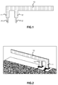
- An example of IFA fabricated using stamping metal technology is shown in Figs 1 and 2.
- Fig.1 shows a 2D view of the antenna and
- Fig.2 shows a 3D perspective view of the antenna mounted on a Printed Circuit Board (PCB).
- PCB Printed Circuit Board
- the antenna contains two vertical metal strips 11 and 12 which are both linked on the top end by a horizontal metal strip 10, forming therefore an inverted F shape. Both vertical strips 11 and 12 are terminated by a pin, P11 and P12 respectively, which are dedicated to be inserted in the respective hole drilled in the PCB.
- the antenna is fed via the pin P12 and the return path to the ground is provided by the pin P11.
- the horizontal strip 10 is a radiating element
- the vertical strip 11 is a ground return element
- the vertical strip 12 is a feeding element.
- the length of the L segment formed by the vertical strip 11 and the horizontal strip 10 is around a quarter of the wavelength, and the distance between the two vertical strips 11 and 12 is tuned commonly in order to achieve the desired impedance matching.
- Fig.2 shows how the IFA is mounted onto a PCB, how it is fed by a micro-strip line and how the grounding pin P11 is connected to the PCB ground plane.
- This antenna operates in the Wi-Fi 2.4GHz band and total length of the resonating element (the L segment) is around 34mm.
- a purpose of the invention is to create a multi-band antenna exhibiting the following characteristics: stamping process compatible, SMD technology compatible, very low profile, high efficiency.
- this antenna is created from a conventional Inverted F antenna (IFA).
- IFA Inverted F antenna
- another resonance frequency is created by increasing strongly the distance between the feeding element and the ground return element of the IFA, achieving thus a dual-band operation.
- the invention relates to an antenna system mounted onto a printed circuit board, said antenna system comprising:
- This antenna operates at least at two operating frequencies, for example at a first frequency in the WiFi band [2.4 GHz - 2.5 GHz] and at a second frequency in the WiFi band [5.15 GHz - 5.85 GHz].
- This antenna is of SMD-type and can be easily manufactured by a stamping process.
- the second radiating element is U-shaped for compactness reason.
- the antenna feeding element and the ground return element are L-bended in order to reduce the height of the antenna system and to achieve a low-profile antenna design.
- the antenna system further comprises a third radiating element having first and second ends, the first end of the third radiating element being connected to the second end of the second radiating element.
- the third radiating element, the second radiating element, the ground return element and the antenna feeding element are arranged to form an inverted-F antenna resonating at a third resonant frequency in a third frequency band.
- the third resonant frequency is included in the first frequency band i.e. the third frequency band is substantially equal to the first frequency band.
- the third radiating element is L-bended, a portion of the L being parallel to the printed circuit board. It enables to pick and place the antenna by a machine for its connection to the printed circuit board.
- the second end of the first radiating element is connected to an open circuit element soldered to an open circuit pad of the printed circuit board. It can help to better hold in place the antenna on the printed circuit board during the soldering process.
- the invention also concerns a device comprising a printed circuit board and an antenna system as defined hereinabove, said antenna system being mounted on said printed circuit board.
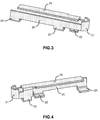
- FIG.3 A first embodiment of the antenna system according to the invention is illustrated by Figs.3 and 4 .
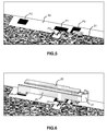
- This antenna system is mounted on a printed circuit board 30 as shown in Figs.5 and 6 .
- the antenna system comprises a vertical metal strip comprising a first portion, called radiating element 20 and a second portion, called radiating element 21. It further comprises three vertical metal strips, i.e. an antenna feeding element 22, a ground return element 23 and an open circuit element 24.
- the radiating element 20 is connected, at a first end, to the upper end of the antenna feeding element 22 and, at a second end, to the upper end of the open circuit element 24.
- the lower end of the antenna feeding element 22 is connected to an antenna feeding pad P1 of the PCB and the lower end of the open circuit element 24 is connected to an open circuit pad P3 of the PCB.
- the radiating element 21 is connected, at a first end, to the upper end of the antenna feeding element 22 and, at a second end, to the upper end of the ground return element 23.
- the lower end of the ground return element 23 is connected to a grounding pad P2 of the PCB.
- the grounding pad P2 is connected to a ground port G0 of a ground plane 31 of the PCB 30.
- the antenna feeding pad P1 is connected to a feeding port P0 of the PCB via a meander-shaped feeding line.
- the radiating elements 20 and 21, the antenna feeding element 22 and the ground return element 23 are arranged to form an inverted-F antenna resonating at a first resonant frequency in a first frequency band, called B1.
- the total length of the elements 20, 21 and 23 is thus around a quarter of the wavelength associated to the first resonant frequency.
- the first resonant frequency is for example a frequency in the WiFi band [2.4GHz-2.5GHz].
- the antenna feeding element 22, the radiating element 21 and the ground return element 23 are arranged to form a loop antenna resonating at a second resonant frequency in a second band frequency, called B2.
- the total length of the elements 22, 21 and 23 is thus around a half of the wavelength associated to the second resonant frequency.
- the band B2 is higher than the band B1.
- the second resonant frequency is for example a frequency in the WiFi band [5.15GHz-5.85GHz].
- the radiating element 21 is advantageously U-shaped for compactness reason.
- the antenna feeding element 22, the ground return element 23 and the open circuit element 24 are preferably L-bended in order to reduce the height of the antenna system and to achieve a low-profile antenna design.
- the radiating element 20 is not connected to the open circuit element 24. In this case, one end of the radiating element 20 is open-ended.
- an open circuit element 24 is to better hold in place the antenna system on the PCB during the soldering process.
- the antenna system further comprises a third radiating element, referenced 25.
- a first end of the radiating element 25 is connected to the radiating element 21 and the other end is open-ended.
- the radiating elements 21 and 25, the ground return element 23 and the antenna feeding element 22 are arranged to form an inverted-F antenna resonating at a third resonant frequency in a third frequency band, called B3.
- the total length of the elements 21, 22 and 25 is thus around a quarter of the wavelength associated to the third resonant frequency.
- the third resonant frequency is included in the band B1 or in the band B2.
- the third resonant frequency is for example included in the WiFi band [2.4GHz-2.5GHz].
- the third resonant frequency is close to the first resonant frequency in the band B1. It enables to increase the impedance matching bandwidth of the antenna system in the band B1.
- the radiating element 25 is advantageously L-bended as illustrated by Figs.3 to 6 .
- a portion of the L is plane and parallel to the surface of the printed circuit board. It enables to pick and place the antenna system by a machine for its connection to the printed circuit board 30.
- the location and the size of the pads and the ports on the PCB are defined in order to optimize the operation of the antenna system.
- the size of the pad P1 has a sensitive influence on the antenna response in the band B2 (high band). Thus it can be optimized in order to improve the impedance matching in this band.
- the length, width and location parameters of the interconnection line printed between the pad P2 and the grounding port G0 is also a means to fine tune the antenna input impedance in the band B2.
- the distance between the feeding port P0 and the grounding port G0 is also critical in the band B2 since it enables also to fine tune the antenna impedance matching in this band. Moreover, tuning the width of the feeding pad P1 has an effect on the antenna response in the band B2.
- the antenna response in the low operation band B1 can be optimized in several ways:
- the antenna system of Figs.3 to 6 has been designed for operating in the two WiFi bands [2.4GHz-2.5GHz] and [5.15GHz-5.85GHz].
- This antenna system mounted on a PCB and arranged within a housing has been simulated using the HFSS TM 3D electromagnetic simulation tool.
- the dimensions of the housing are: 85 x 85 x 15 mm 3 , and those of the PCB are 80*80*1.2 mm 3 .
- the PCB substrate is FR4 based. Simulation results are shown in the graphs of Fig.7, Fig.8 and Fig.9 .
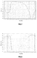
- Fig.7 shows the return loss response of the antenna system. This graph shows that the antenna system is well matched in the both WiFi frequency bands [2.4GHz-2.5GHz] and [5.15GHz-5.85GHz].
- the antenna efficiency plotted in Fig.8 shows remarkable levels, higher than 85% in the worst case.
- Fig.9 shows the peak gain response in the two bands [2.4GHz-2.5GHz] and [5.15GHz-5.85GHz].
- the achieved peak gains are around 2.5dBi and 4.5dBi in the bands [2.4GHz-2.5GHz] and [5.15GHz-5.85GHz] respectively.
- this antenna design can also be arranged for working in three frequency bands B1 to B3.
- the radiating element 25 is sized in order to resonate in a band B3 located between B1 and B2 or lower than B1.
- the antenna design can also be modified as shown in Fig.10 and Fig.11 .
- the radiating element 21 makes a U-turn on the right side (while it makes a U-turn on the left side in the embodiment of Figs.3 and 4 ).
- This antenna system may be mounted on a printed circuit board of any type of home-networking devices, like set-top boxes, gateways or tablets.
Landscapes
- Engineering & Computer Science (AREA)
- Computer Networks & Wireless Communication (AREA)
- Details Of Aerials (AREA)
- Support Of Aerials (AREA)
Abstract
The invention relates to an antenna system mounted onto a printed circuit board (30), said antenna system comprising first and radiating elements (20,21), an antenna feeding element (22) connected to an antenna feeding pad (P1) of the printed circuit board, a ground return element (23) connected to a ground pad (P2) of the printed circuit board. According to the invention, the first and second radiating elements (20, 21), the antenna feeding element (22) and the ground return element (23) are arranged to form an inverted-F antenna resonating at a first resonant frequency in a first frequency band (B1). In addition, the antenna feeding element (22), the second radiating element (21) and the ground return element (23) are arranged to form a loop antenna resonating at a second resonant frequency in a second frequency band (B2), the second frequency band (B2) being above the first frequency band (B1).
Description
- The present invention relates generally to a multi-band antenna for wireless systems, for example for home-networking devices or mobile devices. More specifically, the antenna system of the present invention can be used in set-top boxes, gateways or tablets.
- Home-networking devices, such as gateways and set-top-boxes, needs to be compatible with a plurality of wireless standards and/or a plurality of operating frequency bands for a given standard. Therefore these devices need to have antennas designed for operating at different frequency bands. The invention will be more specifically described for WiFi applications. In the framework of this application, the antennas have to address the IEEE.802.11a/b/g/n/ac standards, meaning a dual-band antenna operating in the [2.4-2.5] GHz and [5.15-5.85] GHz bands.
- As this antenna is deemed to be put in a box and to be connected to a printed circuit board, different requirements have been defined for this antenna:
- use of a 3D antenna metal technology;
- low-profile or low-height antenna design;
- surface mountable on board (SMD-type) antenna;
- stamping process compatible.
- The idea of the invention is to design such an antenna from a classical inverted F antenna (IFA), which primary provides a single band operation. An example of IFA fabricated using stamping metal technology is shown in
Figs 1 and 2. Fig.1 shows a 2D view of the antenna andFig.2 shows a 3D perspective view of the antenna mounted on a Printed Circuit Board (PCB). - In reference to
Figs.1 and 2 , the antenna contains twovertical metal strips horizontal metal strip 10, forming therefore an inverted F shape. Bothvertical strips horizontal strip 10 is a radiating element, thevertical strip 11 is a ground return element and thevertical strip 12 is a feeding element. - As known by people skilled in the art, the length of the L segment formed by the
vertical strip 11 and thehorizontal strip 10 is around a quarter of the wavelength, and the distance between the twovertical strips Fig.2 shows how the IFA is mounted onto a PCB, how it is fed by a micro-strip line and how the grounding pin P11 is connected to the PCB ground plane. This antenna operates in the Wi-Fi 2.4GHz band and total length of the resonating element (the L segment) is around 34mm. - A purpose of the invention is to create a multi-band antenna exhibiting the following characteristics: stamping process compatible, SMD technology compatible, very low profile, high efficiency.
- According to the invention, this antenna is created from a conventional Inverted F antenna (IFA). According to the invention, another resonance frequency is created by increasing strongly the distance between the feeding element and the ground return element of the IFA, achieving thus a dual-band operation.
- More specifically, the invention relates to an antenna system mounted onto a printed circuit board, said antenna system comprising:
- a first radiating element having first and second ends,
- an antenna feeding element connected, at a first end, to the second end of the first radiating element and, at a second end, to an antenna feeding pad of the printed circuit board,
- a second radiating element having first and second ends, the first end of the second radiating element being connected to the second end of the first radiating element,
- a ground return element connected, at a first end, to the second end of the second radiating element and, at a second end, to a ground pad of the printed circuit board,
- This antenna operates at least at two operating frequencies, for example at a first frequency in the WiFi band [2.4 GHz - 2.5 GHz] and at a second frequency in the WiFi band [5.15 GHz - 5.85 GHz]. This antenna is of SMD-type and can be easily manufactured by a stamping process.
- According to a particular embodiment, the second radiating element is U-shaped for compactness reason.
- According to a particular embodiment, the antenna feeding element and the ground return element are L-bended in order to reduce the height of the antenna system and to achieve a low-profile antenna design.
- According to a particular embodiment, the antenna system further comprises a third radiating element having first and second ends, the first end of the third radiating element being connected to the second end of the second radiating element. In this embodiment, the third radiating element, the second radiating element, the ground return element and the antenna feeding element are arranged to form an inverted-F antenna resonating at a third resonant frequency in a third frequency band.
- In case of a dual-band antenna, the third resonant frequency is included in the first frequency band i.e. the third frequency band is substantially equal to the first frequency band.
- According to a particular embodiment, the third radiating element is L-bended, a portion of the L being parallel to the printed circuit board. It enables to pick and place the antenna by a machine for its connection to the printed circuit board.
- According to a particular embodiment, the second end of the first radiating element is connected to an open circuit element soldered to an open circuit pad of the printed circuit board. It can help to better hold in place the antenna on the printed circuit board during the soldering process.
- The invention also concerns a device comprising a printed circuit board and an antenna system as defined hereinabove, said antenna system being mounted on said printed circuit board.
- The invention can be better understood with reference to the following description and drawings, given by way of example and not limiting the scope of protection, and in which:
-
Fig. 1 is a 2D view of an inverted F antenna of the prior art; -
Fig. 2 is a 3D view of the inverted F antenna ofFig.1 mounted on a printed circuit board; -
Fig. 3 is a first perspective view of an antenna system according to a first embodiment of the invention; -
Fig. 4 is a second perspective view of the antenna system ofFig.3 ; -
Fig.5 is a partial view of a printed circuit board whereon the antenna system ofFig.3 and Fig.4 can be mounted; -
Fig.6 is a view of the printed circuit board ofFig.5 whereon the antenna system ofFig.3 and Fig.4 is mounted; -
Fig.7 is a diagram showing the reflection coefficient response of the antenna system ofFig.3 and fig.4 mounted on the printed circuit board ofFig.5 ; -
Fig.8 is a diagram showing the efficiency response of the antenna system ofFig.3 and fig.4 in the bands [2.4 GHz - 2.5 GHz] and [5.15 GHz - 5.85 GHz]; -
Fig.9 is a diagram showing the peak gain response of the antenna system ofFig.3 and fig.4 in the bands [2.4 GHz - 2.5 GHz] and [5.15 GHz - 5.85 GHz]; -
Fig. 10 is a first perspective view of an antenna system according to a second embodiment of the invention mounted on a printed circuit board; and -
Fig. 11 is a second perspective view of the antenna system ofFig.10 . - While example embodiments are capable of various modifications and alternative forms, embodiments thereof are shown by way of example in the drawings and will herein be described in details. It should be understood, however, that there is no intent to limit example embodiments to the particular forms disclosed, but on the contrary, example embodiments are to cover all modifications, equivalents, and alternatives falling within the scope of the claims.
- A first embodiment of the antenna system according to the invention is illustrated by
Figs.3 and 4 . This antenna system is mounted on a printedcircuit board 30 as shown inFigs.5 and 6 . - Referring to
Figs.3 to 6 , the antenna system comprises a vertical metal strip comprising a first portion, called radiatingelement 20 and a second portion, called radiatingelement 21. It further comprises three vertical metal strips, i.e. anantenna feeding element 22, aground return element 23 and anopen circuit element 24. - The radiating
element 20 is connected, at a first end, to the upper end of theantenna feeding element 22 and, at a second end, to the upper end of theopen circuit element 24. The lower end of theantenna feeding element 22 is connected to an antenna feeding pad P1 of the PCB and the lower end of theopen circuit element 24 is connected to an open circuit pad P3 of the PCB. The radiatingelement 21 is connected, at a first end, to the upper end of theantenna feeding element 22 and, at a second end, to the upper end of theground return element 23. The lower end of theground return element 23 is connected to a grounding pad P2 of the PCB. - The grounding pad P2 is connected to a ground port G0 of a
ground plane 31 of thePCB 30. The antenna feeding pad P1 is connected to a feeding port P0 of the PCB via a meander-shaped feeding line. - The radiating
elements antenna feeding element 22 and theground return element 23 are arranged to form an inverted-F antenna resonating at a first resonant frequency in a first frequency band, called B1. The total length of theelements - In addition, the
antenna feeding element 22, the radiatingelement 21 and theground return element 23 are arranged to form a loop antenna resonating at a second resonant frequency in a second band frequency, called B2. The total length of theelements - As illustrated in these figures, the radiating
element 21 is advantageously U-shaped for compactness reason. Theantenna feeding element 22, theground return element 23 and theopen circuit element 24 are preferably L-bended in order to reduce the height of the antenna system and to achieve a low-profile antenna design. - In a variant, the radiating
element 20 is not connected to theopen circuit element 24. In this case, one end of the radiatingelement 20 is open-ended. - In the illustrated antenna system, the main purpose of an
open circuit element 24 is to better hold in place the antenna system on the PCB during the soldering process. - As shown in the
Figs.3 to 6 , the antenna system further comprises a third radiating element, referenced 25. A first end of the radiatingelement 25 is connected to the radiatingelement 21 and the other end is open-ended. The radiatingelements ground return element 23 and theantenna feeding element 22 are arranged to form an inverted-F antenna resonating at a third resonant frequency in a third frequency band, called B3. The total length of theelements - In the case of a dual-band antenna, the third resonant frequency is included in the band B1 or in the band B2. The third resonant frequency is for example included in the WiFi band [2.4GHz-2.5GHz]. In that case, the third resonant frequency is close to the first resonant frequency in the band B1. It enables to increase the impedance matching bandwidth of the antenna system in the band B1.
- The radiating
element 25 is advantageously L-bended as illustrated byFigs.3 to 6 . A portion of the L is plane and parallel to the surface of the printed circuit board. It enables to pick and place the antenna system by a machine for its connection to the printedcircuit board 30. - The location and the size of the pads and the ports on the PCB are defined in order to optimize the operation of the antenna system. The size of the pad P1 has a sensitive influence on the antenna response in the band B2 (high band). Thus it can be optimized in order to improve the impedance matching in this band. In the same manner, the length, width and location parameters of the interconnection line printed between the pad P2 and the grounding port G0 is also a means to fine tune the antenna input impedance in the band B2.
- The distance between the feeding port P0 and the grounding port G0 is also critical in the band B2 since it enables also to fine tune the antenna impedance matching in this band. Moreover, tuning the width of the feeding pad P1 has an effect on the antenna response in the band B2.
- The antenna response in the low operation band B1 can be optimized in several ways:
- by tuning the length and width of the radiating
elements - by adjusting the coupling (the air gap) between the radiating
elements - by tuning the impedance of the meander-shaped feeding line, from P0 to the pad P1.
- The antenna system of
Figs.3 to 6 has been designed for operating in the two WiFi bands [2.4GHz-2.5GHz] and [5.15GHz-5.85GHz]. The antenna system illustrated by these figures has the following sizes: length L=24.75 mm, width W=3.7 mm and height H=4.5 mm. - This antenna system mounted on a PCB and arranged within a housing has been simulated using the HFSS™ 3D electromagnetic simulation tool. The dimensions of the housing are: 85 x 85 x 15 mm3, and those of the PCB are 80*80*1.2 mm3. The PCB substrate is FR4 based. Simulation results are shown in the graphs of
Fig.7, Fig.8 andFig.9 . -
Fig.7 shows the return loss response of the antenna system. This graph shows that the antenna system is well matched in the both WiFi frequency bands [2.4GHz-2.5GHz] and [5.15GHz-5.85GHz]. - The antenna efficiency plotted in
Fig.8 shows remarkable levels, higher than 85% in the worst case. -
Fig.9 shows the peak gain response in the two bands [2.4GHz-2.5GHz] and [5.15GHz-5.85GHz]. The achieved peak gains are around 2.5dBi and 4.5dBi in the bands [2.4GHz-2.5GHz] and [5.15GHz-5.85GHz] respectively. - These graphs show the good efficiency of the antenna system of
Figs.3 to 6 in the bands B1 and B2. - Of course, this antenna design can also be arranged for working in three frequency bands B1 to B3. In that case, the radiating
element 25 is sized in order to resonate in a band B3 located between B1 and B2 or lower than B1. - The antenna design can also be modified as shown in
Fig.10 and Fig.11 . In these figures, the radiatingelement 21 makes a U-turn on the right side (while it makes a U-turn on the left side in the embodiment ofFigs.3 and 4 ). - This antenna system may be mounted on a printed circuit board of any type of home-networking devices, like set-top boxes, gateways or tablets.
wherein the antenna feeding element, the second radiating element and the ground return element are arranged to form a loop antenna resonating at a second resonant frequency in a second frequency band, the second frequency band being above the first frequency band.
Claims (8)
- An antenna system mounted onto a printed circuit board (30), said antenna system comprising:- a first radiating element (20) having first and second ends,- an antenna feeding element (22) connected, at a first end, to the second end of the first radiating element (20) and, at a second end, to an antenna feeding pad (P1) of the printed circuit board,- a second radiating element (21) having first and second ends, the first end of the second radiating element being connected to the second end of the first radiating element (20),- a ground return element (23) connected, at a first end, to the second end of the second radiating element (21) and, at a second end, to a ground pad (P2) of the printed circuit board,wherein the first radiating element (20), the second radiating element (21), the antenna feeding element (22) and the ground return element (23) are arranged to form an inverted-F antenna resonating at a first resonant frequency in a first frequency band (B1), and
wherein the antenna feeding element (22), the second radiating element (21) and the ground return element (23) are arranged to form a loop antenna resonating at a second resonant frequency in a second frequency band (B2), the second frequency band (B2) being above the first frequency band (B1). - Antenna system according to claim 1, wherein the second radiating element (21) is U-shaped.
- Antenna system according to any one of the preceding claims, wherein the antenna feeding element (22) and the ground return element (23) are L-bended.
- Antenna system according to any one of the preceding claims, wherein it further comprises a third radiating element (25) having first and second ends, the first end of the third radiating element being connected to the second end of the second radiating element (21),
and wherein the third radiating element (25), the second radiating element (21), the ground return element (23) and the antenna feeding element (22) are arranged to form an inverted-F antenna resonating at a third resonant frequency in a third frequency band (B3). - Antenna system according to claim 4, wherein the third frequency band is the first frequency band (B1).
- Antenna system according to claim 4 or 5, wherein third radiating element (25) is L-bended, a portion of the L being parallel to the printed circuit board.
- Antenna system according to any one of the preceding claims, wherein the second end of the first radiating element (20) is connected to an open circuit element (24).
- Device comprising a printed circuit board, wherein it further comprises an antenna system according to any one of claims 1 to 7, said antenna system being mounted on said printed circuit board.
Priority Applications (4)
| Application Number | Priority Date | Filing Date | Title |
|---|---|---|---|
| EP16305326.7A EP3223362A1 (en) | 2016-03-23 | 2016-03-23 | Low-profile multi-band antenna |
| US16/087,128 US20190081388A1 (en) | 2016-03-23 | 2017-03-21 | Low-profile multi-band antenna |
| EP17712497.1A EP3433898A1 (en) | 2016-03-23 | 2017-03-21 | Low-profile multi-band antenna |
| PCT/EP2017/056738 WO2017162695A1 (en) | 2016-03-23 | 2017-03-21 | Low-profile multi-band antenna |
Applications Claiming Priority (1)
| Application Number | Priority Date | Filing Date | Title |
|---|---|---|---|
| EP16305326.7A EP3223362A1 (en) | 2016-03-23 | 2016-03-23 | Low-profile multi-band antenna |
Publications (1)
| Publication Number | Publication Date |
|---|---|
| EP3223362A1 true EP3223362A1 (en) | 2017-09-27 |
Family
ID=55640657
Family Applications (2)
| Application Number | Title | Priority Date | Filing Date |
|---|---|---|---|
| EP16305326.7A Withdrawn EP3223362A1 (en) | 2016-03-23 | 2016-03-23 | Low-profile multi-band antenna |
| EP17712497.1A Withdrawn EP3433898A1 (en) | 2016-03-23 | 2017-03-21 | Low-profile multi-band antenna |
Family Applications After (1)
| Application Number | Title | Priority Date | Filing Date |
|---|---|---|---|
| EP17712497.1A Withdrawn EP3433898A1 (en) | 2016-03-23 | 2017-03-21 | Low-profile multi-band antenna |
Country Status (3)
| Country | Link |
|---|---|
| US (1) | US20190081388A1 (en) |
| EP (2) | EP3223362A1 (en) |
| WO (1) | WO2017162695A1 (en) |
Cited By (2)
| Publication number | Priority date | Publication date | Assignee | Title |
|---|---|---|---|---|
| CN108574142A (en) * | 2017-11-23 | 2018-09-25 | 上海龙晶科技有限公司 | An on-board antenna of an OTT set-top box |
| WO2019196102A1 (en) * | 2018-04-13 | 2019-10-17 | 华为技术有限公司 | Antenna and electronic device |
Families Citing this family (3)
| Publication number | Priority date | Publication date | Assignee | Title |
|---|---|---|---|---|
| EP3261172B1 (en) * | 2016-06-21 | 2020-07-29 | Axis AB | Pcb antenna |
| US11239560B2 (en) * | 2017-12-14 | 2022-02-01 | Desarrollo De Tecnologia E Informätica Aplicada, S.A.P.I. De C.V. | Ultra wide band antenna |
| CN121729800A (en) * | 2023-08-23 | 2026-03-24 | 住友电气工业株式会社 | Antenna and antenna member |
Citations (5)
| Publication number | Priority date | Publication date | Assignee | Title |
|---|---|---|---|---|
| EP1555715A1 (en) * | 2004-01-13 | 2005-07-20 | Kabushiki Kaisha Toshiba | Antenna device and mobile communication terminal equipped with antenna device |
| US20090040110A1 (en) * | 2007-08-09 | 2009-02-12 | Chin-Cheng Chien | Multi-band planar inverted-f antenna |
| EP2328233A2 (en) * | 2009-11-27 | 2011-06-01 | Fujitsu Limited | Antenna and radio communication apparatus |
| US20120007784A1 (en) * | 2010-07-09 | 2012-01-12 | Ching-Wei Ling | Inverted-f antenna and wireless communication apparatus using the same |
| US20150116168A1 (en) * | 2012-12-21 | 2015-04-30 | Murata Manufacturing Co., Ltd. | Antenna device and electronic apparatus |
-
2016
- 2016-03-23 EP EP16305326.7A patent/EP3223362A1/en not_active Withdrawn
-
2017
- 2017-03-21 US US16/087,128 patent/US20190081388A1/en not_active Abandoned
- 2017-03-21 WO PCT/EP2017/056738 patent/WO2017162695A1/en not_active Ceased
- 2017-03-21 EP EP17712497.1A patent/EP3433898A1/en not_active Withdrawn
Patent Citations (5)
| Publication number | Priority date | Publication date | Assignee | Title |
|---|---|---|---|---|
| EP1555715A1 (en) * | 2004-01-13 | 2005-07-20 | Kabushiki Kaisha Toshiba | Antenna device and mobile communication terminal equipped with antenna device |
| US20090040110A1 (en) * | 2007-08-09 | 2009-02-12 | Chin-Cheng Chien | Multi-band planar inverted-f antenna |
| EP2328233A2 (en) * | 2009-11-27 | 2011-06-01 | Fujitsu Limited | Antenna and radio communication apparatus |
| US20120007784A1 (en) * | 2010-07-09 | 2012-01-12 | Ching-Wei Ling | Inverted-f antenna and wireless communication apparatus using the same |
| US20150116168A1 (en) * | 2012-12-21 | 2015-04-30 | Murata Manufacturing Co., Ltd. | Antenna device and electronic apparatus |
Cited By (2)
| Publication number | Priority date | Publication date | Assignee | Title |
|---|---|---|---|---|
| CN108574142A (en) * | 2017-11-23 | 2018-09-25 | 上海龙晶科技有限公司 | An on-board antenna of an OTT set-top box |
| WO2019196102A1 (en) * | 2018-04-13 | 2019-10-17 | 华为技术有限公司 | Antenna and electronic device |
Also Published As
| Publication number | Publication date |
|---|---|
| WO2017162695A1 (en) | 2017-09-28 |
| EP3433898A1 (en) | 2019-01-30 |
| US20190081388A1 (en) | 2019-03-14 |
Similar Documents
| Publication | Publication Date | Title |
|---|---|---|
| US9590304B2 (en) | Broadband antenna | |
| US9711857B2 (en) | Multi-band antenna | |
| TWI489690B (en) | Multi-band planar inverted-f (pifa) antennas and systems with improved isolation | |
| EP1791213A1 (en) | Multiband antenna component | |
| US8779985B2 (en) | Dual radiator monopole antenna | |
| TWI631770B (en) | Dual-band dual-port antenna structure | |
| US8593352B2 (en) | Triple-band antenna with low profile | |
| US20190081388A1 (en) | Low-profile multi-band antenna | |
| US8441399B2 (en) | Three-dimensional slot antenna | |
| US9620863B2 (en) | Antenna device | |
| EP2808942B1 (en) | Antenna structure | |
| TW202121743A (en) | Antenna structure and electronic device | |
| US8013793B2 (en) | Multi-band antenna | |
| US20140071014A1 (en) | Multi-band antenna | |
| US8035566B2 (en) | Multi-band antenna | |
| TW202036986A (en) | Dual-band antenna | |
| US8723754B2 (en) | Multi-band antenna | |
| US8754821B2 (en) | Multi-band antenna | |
| KR20190086183A (en) | Multi-band slot antenna | |
| US9472847B2 (en) | Antenna structure and wireless communication device employing same | |
| KR20180094636A (en) | Antenna apparatus | |
| TW201703347A (en) | Printed multi-band antenna | |
| EP2800202B1 (en) | Communication device with ground plane antenna | |
| TWI580111B (en) | Communication device | |
| US20250246816A1 (en) | Electronic device |
Legal Events
| Date | Code | Title | Description |
|---|---|---|---|
| PUAI | Public reference made under article 153(3) epc to a published international application that has entered the european phase |
Free format text: ORIGINAL CODE: 0009012 |
|
| AK | Designated contracting states |
Kind code of ref document: A1 Designated state(s): AL AT BE BG CH CY CZ DE DK EE ES FI FR GB GR HR HU IE IS IT LI LT LU LV MC MK MT NL NO PL PT RO RS SE SI SK SM TR |
|
| AX | Request for extension of the european patent |
Extension state: BA ME |
|
| STAA | Information on the status of an ep patent application or granted ep patent |
Free format text: STATUS: THE APPLICATION IS DEEMED TO BE WITHDRAWN |
|
| 18D | Application deemed to be withdrawn |
Effective date: 20180328 |