EP3223317A1 - Optocoupler - Google Patents
Optocoupler Download PDFInfo
- Publication number
- EP3223317A1 EP3223317A1 EP16161321.1A EP16161321A EP3223317A1 EP 3223317 A1 EP3223317 A1 EP 3223317A1 EP 16161321 A EP16161321 A EP 16161321A EP 3223317 A1 EP3223317 A1 EP 3223317A1
- Authority
- EP
- European Patent Office
- Prior art keywords
- housing
- coating
- optocoupler
- infrared radiation
- transmitter
- Prior art date
- Legal status (The legal status is an assumption and is not a legal conclusion. Google has not performed a legal analysis and makes no representation as to the accuracy of the status listed.)
- Granted
Links
Images
Classifications
-
- H—ELECTRICITY
- H10—SEMICONDUCTOR DEVICES; ELECTRIC SOLID-STATE DEVICES NOT OTHERWISE PROVIDED FOR
- H10F—INORGANIC SEMICONDUCTOR DEVICES SENSITIVE TO INFRARED RADIATION, LIGHT, ELECTROMAGNETIC RADIATION OF SHORTER WAVELENGTH OR CORPUSCULAR RADIATION
- H10F55/00—Radiation-sensitive semiconductor devices covered by groups H10F10/00, H10F19/00 or H10F30/00 being structurally associated with electric light sources and electrically or optically coupled thereto
- H10F55/20—Radiation-sensitive semiconductor devices covered by groups H10F10/00, H10F19/00 or H10F30/00 being structurally associated with electric light sources and electrically or optically coupled thereto wherein the electric light source controls the radiation-sensitive semiconductor devices, e.g. optocouplers
- H10F55/25—Radiation-sensitive semiconductor devices covered by groups H10F10/00, H10F19/00 or H10F30/00 being structurally associated with electric light sources and electrically or optically coupled thereto wherein the electric light source controls the radiation-sensitive semiconductor devices, e.g. optocouplers wherein the radiation-sensitive devices and the electric light source are all semiconductor devices
-
- H—ELECTRICITY
- H10—SEMICONDUCTOR DEVICES; ELECTRIC SOLID-STATE DEVICES NOT OTHERWISE PROVIDED FOR
- H10F—INORGANIC SEMICONDUCTOR DEVICES SENSITIVE TO INFRARED RADIATION, LIGHT, ELECTROMAGNETIC RADIATION OF SHORTER WAVELENGTH OR CORPUSCULAR RADIATION
- H10F77/00—Constructional details of devices covered by this subclass
- H10F77/30—Coatings
Definitions
- the invention relates to an optocoupler comprising a transmitter as well as a receiver optically connected with one another and disposed in a housing comprising a transparent housing wall.
- An optocoupler is a component of optoelectronics. It serves for transmitting a signal between two electrically isolated circuits.
- An optocoupler is conventionally comprised of a light-emitting diode (LED) or a laser diode (LD) as the optical transmitter and a photodiode or a phototransistor as the optical receiver.
- the optically coupled transmitter component and receiver component are located in a housing opaque to incident light.
- Conventional optocouplers include an opaque housing in the form of a bulky metal casing or in the form of an equally bulky combination comprised of an inner housing of a synthetic material that is transparent to the infrared light used for the transmission, which housing is intended for receiving or for mounting the transmitter and the receiver, and an additional outer synthetic housing transparent in the infrared range.
- the present invention addresses the problem of providing an optocoupler that has a simple structure and is also not prone to interference by infrared radiation.
- a housing with a housing wall is provided, wherein onto the housing wall at least one coating is applied that is opaque to infrared radiation.
- the invention thus relates to an optocoupler comprising a transmitter as well as a receiver which are optically connected with one another.
- the transmitter as well as the receiver are embedded in a housing comprised of a housing wall which is transparent and thus permeable to light.
- the housing comprises at least one coating that is opaque to infrared radiation so that no infrared radiation can penetrate into the housing from the outside. Since no infrared radiation can reach the inside of the housing, this optocoupler is not prone to interference due to infrared radiation.
- a further advantage comprises that the optocoupler is of simple structure and can be small-dimensioned since only one housing is provided that has a housing wall and since onto this housing wall a coating opaque to infrared radiation is applied.
- the housing of the optocoupler consequently can simply be provided with at least one coating before the transmitter and the receiver are installed in the housing.
- the at least one coating is preferably an absorption layer.
- This coating consequently absorbs infrared ration.
- suitable lacquers or varnishes comprising, for example, a 2k polyurethane acrylic system. This system involves a coating that has a simple structure and, at the same time, can be applied quickly yet provides optimum protection against infrared radiation.
- the at least one coating is a reflection layer reflecting the infrared radiation.
- the reflection layer preferably lacquers or varnishes are employed. Such a coating is cost-effective and can be simply structured.
- the coating impermeable to infrared radiation can be applied on an outer side and/or on an inner side of the transparent housing wall of the housing. It is consequently irrelevant whether the coating is applied on the outer side or on the inner side as long as the applied coating prevents infrared radiation from penetrating into the interior of the housing and, in doing so, interferes with the transmission path. It is herein especially advantageous if the infrared radiation-opaque coating is applied on the inner side as well as also on the outer side of the housing wall whereby even better protection can be insured. It is, for example, feasible to apply a reflection layer on the outer side and an absorption layer on the inner side of the housing wall of the housing.
- the coating is preferably a lacquer or varnish layer.
- a lacquer or varnish layer is fairly cost-effective and can especially simply be applied onto the housing wall.
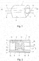
- FIG. 1 shows a perspective view onto an optocoupler 1.
- the optocoupler 1 comprises a housing 2 with a housing wall 8 comprised of a transparent material.
- the housing wall 8 is preferably comprised of a synthetic material, such as for example acrylic resin, transparent to light.
- a transmitter and a receiver are provided, which, however, are not visible.
- From the housing 2 two terminals 3, 4 of the transmitter and two terminals 5, 6 of the receiver project from apertures of housing 2.
- the transmitter is preferably an optical transmitter which can be a light-emitting diode (LED) or a laser diode (LD).
- the receiver involves an optical receiver, preferably a photodiode or a phototransistor.
- FIG 2 is depicted a section A-A through the optocoupler 1 shown in Figure 1 .
- the housing 2 has two oppositely located apertures 7, 16 from which the corresponding terminals of transmitter 11 or of receiver 12 can extend from housing 2. However, the section only shows terminal 4 of the transmitter 11 as well as terminal 5 of the receiver 12.
- the housing 2 comprises the housing wall 8 comprised of a transparent material, preferably of a transparent synthetic material. Since this housing wall 8 is transparent to infrared radiation, an outer coating 9 is applied onto this housing wall 8. This coating 9 is opaque to infrared radiation.
- the infrared radiation-opaque coating can be a lacquer or varnish layer which absorbs or reflects infrared radiation.
- Housing 2 comprises an inner region 10 which is divided into a first subsection 14 and a second subsection 15. In the first subsection 14 is located the transmitter 11 and in the second subsection 15 the receiver 12. Between the first subsection 14 and the second subsection 15 a separating wall 13 is provided which is transparent to light and, in particular, to infrared radiation so that the optical transmitter 11 can communicate with the optical receiver 12.
- the separating wall 13 is herein preferably comprised of the same material as the housing wall 8. To prevent the transmitter 11 and the receiver 12 from sliding in the interior region 10 of housing 2, the interior region 10 is developed such that transmitter 11 as well as receiver 12 are clamped in housing 2 and are thus fixed.
- the housing 2 includes a first aperture 7 as well as a second, oppositely located aperture 16 out of which the corresponding terminals of the transmitter 11 or of the receiver 12 can reach into the housing 2.
- the coating 9 can be applied either on an outer side 17 of housing wall 8 of housing 2 - as is shown in Figure 2 - or on an inner side 18 of housing wall 8. It is also feasible for a coating opaque to infrared radiation to be provided on the outer side 17 as well as also on the inner side 18 of housing wall 8 in order to ensure even better protection against infrared radiation. However, such is not shown in Figure 2 .
- this optocoupler 1 Since no infrared radiation can penetrate into the interior region 10 of housing 2 and therefore can also not reach the receiver 12 or the transmitter 11, this optocoupler 1 is not prone to interference with respect to infrared radiation.
Landscapes
- Photo Coupler, Interrupter, Optical-To-Optical Conversion Devices (AREA)
Abstract
Description
- The invention relates to an optocoupler comprising a transmitter as well as a receiver optically connected with one another and disposed in a housing comprising a transparent housing wall.
- An optocoupler is a component of optoelectronics. It serves for transmitting a signal between two electrically isolated circuits. An optocoupler is conventionally comprised of a light-emitting diode (LED) or a laser diode (LD) as the optical transmitter and a photodiode or a phototransistor as the optical receiver. The optically coupled transmitter component and receiver component are located in a housing opaque to incident light.
Conventional optocouplers include an opaque housing in the form of a bulky metal casing or in the form of an equally bulky combination comprised of an inner housing of a synthetic material that is transparent to the infrared light used for the transmission, which housing is intended for receiving or for mounting the transmitter and the receiver, and an additional outer synthetic housing transparent in the infrared range. - The purpose of these dispositions is to protect the transmission path against external irradiation in order not to "transmit" false signals. However, this assembly is mechanically formidable and complexly structured because of the inner as well as the outer synthetic housing.
- The present invention addresses the problem of providing an optocoupler that has a simple structure and is also not prone to interference by infrared radiation.
- This problem is resolved thereby that a housing with a housing wall is provided, wherein onto the housing wall at least one coating is applied that is opaque to infrared radiation.
- [A01] The invention thus relates to an optocoupler comprising a transmitter as well as a receiver which are optically connected with one another. The transmitter as well as the receiver are embedded in a housing comprised of a housing wall which is transparent and thus permeable to light. The housing comprises at least one coating that is opaque to infrared radiation so that no infrared radiation can penetrate into the housing from the outside. Since no infrared radiation can reach the inside of the housing, this optocoupler is not prone to interference due to infrared radiation. A further advantage comprises that the optocoupler is of simple structure and can be small-dimensioned since only one housing is provided that has a housing wall and since onto this housing wall a coating opaque to infrared radiation is applied. Further restructuring or retrofitting measures do not need to be undertaken since it is not necessary to equip the optocoupler with an inner and an outer housing. The housing of the optocoupler consequently can simply be provided with at least one coating before the transmitter and the receiver are installed in the housing.
- [A02] The at least one coating is preferably an absorption layer. This coating consequently absorbs infrared ration. As the absorption layer are preferably utilized suitable lacquers or varnishes comprising, for example, a 2k polyurethane acrylic system. This system involves a coating that has a simple structure and, at the same time, can be applied quickly yet provides optimum protection against infrared radiation.
- [A03] In a further, preferred embodiment the at least one coating is a reflection layer reflecting the infrared radiation. As the reflection layer preferably lacquers or varnishes are employed. Such a coating is cost-effective and can be simply structured.
- [A04] The coating impermeable to infrared radiation can be applied on an outer side and/or on an inner side of the transparent housing wall of the housing. It is consequently irrelevant whether the coating is applied on the outer side or on the inner side as long as the applied coating prevents infrared radiation from penetrating into the interior of the housing and, in doing so, interferes with the transmission path. It is herein especially advantageous if the infrared radiation-opaque coating is applied on the inner side as well as also on the outer side of the housing wall whereby even better protection can be insured. It is, for example, feasible to apply a reflection layer on the outer side and an absorption layer on the inner side of the housing wall of the housing.
- [A05] The coating is preferably a lacquer or varnish layer. Such a lacquer or varnish layer is fairly cost-effective and can especially simply be applied onto the housing wall.
- An embodiment example is described in further detail in the following in conjunction with Figures. In the drawing depict:
- Figure 1
- a perspective view onto an optocoupler and
- Figure 2
- a section A-A through the optocoupler depicted in
Figure 1 . -
Figure 1 shows a perspective view onto an optocoupler 1. The optocoupler 1 comprises ahousing 2 with ahousing wall 8 comprised of a transparent material. Thehousing wall 8 is preferably comprised of a synthetic material, such as for example acrylic resin, transparent to light. In an interior region of the housing 2 a transmitter and a receiver are provided, which, however, are not visible. From thehousing 2 twoterminals terminals housing 2. However, inFigure 1 only theaperture 7 can be seen.
The transmitter is preferably an optical transmitter which can be a light-emitting diode (LED) or a laser diode (LD). The receiver involves an optical receiver, preferably a photodiode or a phototransistor. - In
Figure 2 is depicted a section A-A through the optocoupler 1 shown inFigure 1 . Thehousing 2 has two oppositely locatedapertures transmitter 11 or ofreceiver 12 can extend fromhousing 2. However, the section only showsterminal 4 of thetransmitter 11 as well asterminal 5 of thereceiver 12. Thehousing 2 comprises thehousing wall 8 comprised of a transparent material, preferably of a transparent synthetic material. Since thishousing wall 8 is transparent to infrared radiation, anouter coating 9 is applied onto thishousing wall 8. Thiscoating 9 is opaque to infrared radiation. - The infrared radiation-opaque coating can be a lacquer or varnish layer which absorbs or reflects infrared radiation.
Housing 2 comprises aninner region 10 which is divided into afirst subsection 14 and asecond subsection 15. In thefirst subsection 14 is located thetransmitter 11 and in thesecond subsection 15 thereceiver 12. Between thefirst subsection 14 and the second subsection 15 aseparating wall 13 is provided which is transparent to light and, in particular, to infrared radiation so that theoptical transmitter 11 can communicate with theoptical receiver 12. The separatingwall 13 is herein preferably comprised of the same material as thehousing wall 8. To prevent thetransmitter 11 and thereceiver 12 from sliding in theinterior region 10 ofhousing 2, theinterior region 10 is developed such thattransmitter 11 as well asreceiver 12 are clamped inhousing 2 and are thus fixed.
Thehousing 2 includes afirst aperture 7 as well as a second, oppositely locatedaperture 16 out of which the corresponding terminals of thetransmitter 11 or of thereceiver 12 can reach into thehousing 2.
Thecoating 9 can be applied either on anouter side 17 ofhousing wall 8 of housing 2 - as is shown inFigure 2 - or on aninner side 18 ofhousing wall 8. It is also feasible for a coating opaque to infrared radiation to be provided on theouter side 17 as well as also on theinner side 18 ofhousing wall 8 in order to ensure even better protection against infrared radiation. However, such is not shown inFigure 2 . - Since no infrared radiation can penetrate into the
interior region 10 ofhousing 2 and therefore can also not reach thereceiver 12 or thetransmitter 11, this optocoupler 1 is not prone to interference with respect to infrared radiation. -
- 1
- Optocoupler
- 2
- Housing
- 3
- Terminal of transmitter
- 4
- Terminal of transmitter
- 5
- Terminal of receiver
- 6
- Terminal of receiver
- 7
- Aperture
- 8
- Housing wall
- 9
- Coating opaque to infrared radiation
- 10
- Interior region
- 11
- Transmitter
- 12
- Receiver
- 13
- Separating wall
- 14
- First subsection
- 15
- Second subsection
- 16
- Aperture
- 17
- Outer side
- 18
- Inner side
Claims (5)
- Optocoupler (1) comprising a transmitter (11) as well as a receiver (12) optically connected with one another and disposed in a housing (2) that includes a housing wall (8) transparent to light, characterized in that on the housing wall (8) at least one coating (9) is applied, wherein the at least one coating (9) is opaque to infrared radiation.
- Optocoupler as in claim 1, characterized in that the at least one coating (9) is an absorption layer.
- Optocoupler as in claim 1, characterized in that the at least one coating (9) is a reflection layer.
- Optocoupler as in claim 1, characterized in that the coating (9) is applied on an outer side (17) and/or on an inner side (18) of the housing wall (8) of the housing (2).
- Optocoupler as in claim 1, characterized in that the coating (9) is a lacquer or varnish layer.
Priority Applications (1)
| Application Number | Priority Date | Filing Date | Title |
|---|---|---|---|
| EP16161321.1A EP3223317B1 (en) | 2016-03-21 | 2016-03-21 | Optocoupler |
Applications Claiming Priority (1)
| Application Number | Priority Date | Filing Date | Title |
|---|---|---|---|
| EP16161321.1A EP3223317B1 (en) | 2016-03-21 | 2016-03-21 | Optocoupler |
Publications (2)
| Publication Number | Publication Date |
|---|---|
| EP3223317A1 true EP3223317A1 (en) | 2017-09-27 |
| EP3223317B1 EP3223317B1 (en) | 2019-01-23 |
Family
ID=55637200
Family Applications (1)
| Application Number | Title | Priority Date | Filing Date |
|---|---|---|---|
| EP16161321.1A Active EP3223317B1 (en) | 2016-03-21 | 2016-03-21 | Optocoupler |
Country Status (1)
| Country | Link |
|---|---|
| EP (1) | EP3223317B1 (en) |
Citations (8)
| Publication number | Priority date | Publication date | Assignee | Title |
|---|---|---|---|---|
| US20110186736A1 (en) * | 2010-01-31 | 2011-08-04 | Avago Technologies Ecbu (Singapore) Pte. Ltd. | Optical Proximity Sensor Package with Lead Frame |
| US20110297832A1 (en) * | 2010-06-08 | 2011-12-08 | Avago Technologies Ecbu Ip (Singapore) Pte. Ltd. | Proximity Sensor |
| US20110297831A1 (en) * | 2010-06-08 | 2011-12-08 | Avago Technologies Ecbu Ip (Singapore) Pte. Ltd. | Small Low-Profile Optical Proximity Sensor |
| US20130292706A1 (en) * | 2009-06-30 | 2013-11-07 | Avago Technologies General Ip (Singapore) Pte. Ltd. | Infrared Attenuating Or Blocking Layer In Optical Proximity Sensor |
| US20140054614A1 (en) * | 2012-08-21 | 2014-02-27 | Kabushiki Kaisha Toshiba | Semiconductor device having optically-coupled element |
| US20140091326A1 (en) * | 2012-10-01 | 2014-04-03 | Texas Instruments Incorporated | Light Blocking Structure in Leadframe |
| JP2014099468A (en) * | 2012-11-13 | 2014-05-29 | Pioneer Electronic Corp | Semiconductor device manufacturing method and semiconductor device |
| WO2015076750A1 (en) * | 2013-11-22 | 2015-05-28 | Heptagon Micro Optics Pte. Ltd. | Compact optoelectronic modules |
Family Cites Families (1)
| Publication number | Priority date | Publication date | Assignee | Title |
|---|---|---|---|---|
| DE3526001A1 (en) * | 1984-12-20 | 1987-02-19 | Werk Fernsehelektronik Veb | High-voltage-resistant optocoupler |
-
2016
- 2016-03-21 EP EP16161321.1A patent/EP3223317B1/en active Active
Patent Citations (8)
| Publication number | Priority date | Publication date | Assignee | Title |
|---|---|---|---|---|
| US20130292706A1 (en) * | 2009-06-30 | 2013-11-07 | Avago Technologies General Ip (Singapore) Pte. Ltd. | Infrared Attenuating Or Blocking Layer In Optical Proximity Sensor |
| US20110186736A1 (en) * | 2010-01-31 | 2011-08-04 | Avago Technologies Ecbu (Singapore) Pte. Ltd. | Optical Proximity Sensor Package with Lead Frame |
| US20110297832A1 (en) * | 2010-06-08 | 2011-12-08 | Avago Technologies Ecbu Ip (Singapore) Pte. Ltd. | Proximity Sensor |
| US20110297831A1 (en) * | 2010-06-08 | 2011-12-08 | Avago Technologies Ecbu Ip (Singapore) Pte. Ltd. | Small Low-Profile Optical Proximity Sensor |
| US20140054614A1 (en) * | 2012-08-21 | 2014-02-27 | Kabushiki Kaisha Toshiba | Semiconductor device having optically-coupled element |
| US20140091326A1 (en) * | 2012-10-01 | 2014-04-03 | Texas Instruments Incorporated | Light Blocking Structure in Leadframe |
| JP2014099468A (en) * | 2012-11-13 | 2014-05-29 | Pioneer Electronic Corp | Semiconductor device manufacturing method and semiconductor device |
| WO2015076750A1 (en) * | 2013-11-22 | 2015-05-28 | Heptagon Micro Optics Pte. Ltd. | Compact optoelectronic modules |
Also Published As
| Publication number | Publication date |
|---|---|
| EP3223317B1 (en) | 2019-01-23 |
Similar Documents
| Publication | Publication Date | Title |
|---|---|---|
| US4051365A (en) | Photoelectric detector having an indicator for indicating the operating condition thereof | |
| KR970011116B1 (en) | Photoelectric sensor | |
| JP3819893B2 (en) | Double-cap bidirectional optical communication module | |
| EP3796033A1 (en) | Optical module with stray light baffle | |
| TWI226135B (en) | Optical link device | |
| US10001590B2 (en) | Optical transmission module | |
| WO2009095384A3 (en) | Device for determining a distance to an object | |
| CN210638715U (en) | Background suppression sensor with strong anti-interference performance | |
| CN207516546U (en) | A kind of micromation laser pulse ranging scanning means | |
| SE9902623D0 (en) | An electric apparatus having visual indicator means | |
| US20170089757A1 (en) | Concealed optoelectronic module | |
| CN109932728A (en) | A kind of micromation laser pulse ranging scanning means | |
| US20180306987A1 (en) | Bidirectional Optical Sub Assembly | |
| US20080187321A1 (en) | Optical transceiver module | |
| US11525905B2 (en) | LIDAR device for detecting an object | |
| EP3223317B1 (en) | Optocoupler | |
| JPH0246113B2 (en) | ||
| CN102843197B (en) | Duplexing light transceiving device body | |
| KR20190012441A (en) | Visible light receiver and visible light communication system comprising the same | |
| CN111868590B (en) | Receiver and light-emitting devices, optical modules and communication equipment | |
| US20230275659A1 (en) | Insulation device incorporated in an optical wireless communication equipment | |
| CN212031795U (en) | Optical assembly and tapered hole core cylinder module thereof | |
| CN215990814U (en) | Anti-interference optical module | |
| WO2005084397A3 (en) | Transmitter and receiver optical sub-assemblies with optical limiting elements | |
| JPH0328789A (en) | Photoelectric sensor |
Legal Events
| Date | Code | Title | Description |
|---|---|---|---|
| PUAI | Public reference made under article 153(3) epc to a published international application that has entered the european phase |
Free format text: ORIGINAL CODE: 0009012 |
|
| STAA | Information on the status of an ep patent application or granted ep patent |
Free format text: STATUS: THE APPLICATION HAS BEEN PUBLISHED |
|
| AK | Designated contracting states |
Kind code of ref document: A1 Designated state(s): AL AT BE BG CH CY CZ DE DK EE ES FI FR GB GR HR HU IE IS IT LI LT LU LV MC MK MT NL NO PL PT RO RS SE SI SK SM TR |
|
| AX | Request for extension of the european patent |
Extension state: BA ME |
|
| STAA | Information on the status of an ep patent application or granted ep patent |
Free format text: STATUS: REQUEST FOR EXAMINATION WAS MADE |
|
| 17P | Request for examination filed |
Effective date: 20171227 |
|
| RBV | Designated contracting states (corrected) |
Designated state(s): AL AT BE BG CH CY CZ DE DK EE ES FI FR GB GR HR HU IE IS IT LI LT LU LV MC MK MT NL NO PL PT RO RS SE SI SK SM TR |
|
| STAA | Information on the status of an ep patent application or granted ep patent |
Free format text: STATUS: EXAMINATION IS IN PROGRESS |
|
| 17Q | First examination report despatched |
Effective date: 20180417 |
|
| GRAP | Despatch of communication of intention to grant a patent |
Free format text: ORIGINAL CODE: EPIDOSNIGR1 |
|
| STAA | Information on the status of an ep patent application or granted ep patent |
Free format text: STATUS: GRANT OF PATENT IS INTENDED |
|
| INTG | Intention to grant announced |
Effective date: 20181004 |
|
| GRAS | Grant fee paid |
Free format text: ORIGINAL CODE: EPIDOSNIGR3 |
|
| GRAA | (expected) grant |
Free format text: ORIGINAL CODE: 0009210 |
|
| STAA | Information on the status of an ep patent application or granted ep patent |
Free format text: STATUS: THE PATENT HAS BEEN GRANTED |
|
| AK | Designated contracting states |
Kind code of ref document: B1 Designated state(s): AL AT BE BG CH CY CZ DE DK EE ES FI FR GB GR HR HU IE IS IT LI LT LU LV MC MK MT NL NO PL PT RO RS SE SI SK SM TR |
|
| REG | Reference to a national code |
Ref country code: GB Ref legal event code: FG4D |
|
| REG | Reference to a national code |
Ref country code: CH Ref legal event code: EP |
|
| REG | Reference to a national code |
Ref country code: AT Ref legal event code: REF Ref document number: 1092143 Country of ref document: AT Kind code of ref document: T Effective date: 20190215 |
|
| REG | Reference to a national code |
Ref country code: IE Ref legal event code: FG4D |
|
| REG | Reference to a national code |
Ref country code: DE Ref legal event code: R096 Ref document number: 602016009332 Country of ref document: DE |
|
| REG | Reference to a national code |
Ref country code: NL Ref legal event code: MP Effective date: 20190123 |
|
| PG25 | Lapsed in a contracting state [announced via postgrant information from national office to epo] |
Ref country code: NL Free format text: LAPSE BECAUSE OF FAILURE TO SUBMIT A TRANSLATION OF THE DESCRIPTION OR TO PAY THE FEE WITHIN THE PRESCRIBED TIME-LIMIT Effective date: 20190123 |
|
| PG25 | Lapsed in a contracting state [announced via postgrant information from national office to epo] |
Ref country code: NO Free format text: LAPSE BECAUSE OF FAILURE TO SUBMIT A TRANSLATION OF THE DESCRIPTION OR TO PAY THE FEE WITHIN THE PRESCRIBED TIME-LIMIT Effective date: 20190423 Ref country code: FI Free format text: LAPSE BECAUSE OF FAILURE TO SUBMIT A TRANSLATION OF THE DESCRIPTION OR TO PAY THE FEE WITHIN THE PRESCRIBED TIME-LIMIT Effective date: 20190123 Ref country code: LT Free format text: LAPSE BECAUSE OF FAILURE TO SUBMIT A TRANSLATION OF THE DESCRIPTION OR TO PAY THE FEE WITHIN THE PRESCRIBED TIME-LIMIT Effective date: 20190123 Ref country code: PL Free format text: LAPSE BECAUSE OF FAILURE TO SUBMIT A TRANSLATION OF THE DESCRIPTION OR TO PAY THE FEE WITHIN THE PRESCRIBED TIME-LIMIT Effective date: 20190123 Ref country code: PT Free format text: LAPSE BECAUSE OF FAILURE TO SUBMIT A TRANSLATION OF THE DESCRIPTION OR TO PAY THE FEE WITHIN THE PRESCRIBED TIME-LIMIT Effective date: 20190523 Ref country code: ES Free format text: LAPSE BECAUSE OF FAILURE TO SUBMIT A TRANSLATION OF THE DESCRIPTION OR TO PAY THE FEE WITHIN THE PRESCRIBED TIME-LIMIT Effective date: 20190123 Ref country code: SE Free format text: LAPSE BECAUSE OF FAILURE TO SUBMIT A TRANSLATION OF THE DESCRIPTION OR TO PAY THE FEE WITHIN THE PRESCRIBED TIME-LIMIT Effective date: 20190123 |
|
| REG | Reference to a national code |
Ref country code: AT Ref legal event code: MK05 Ref document number: 1092143 Country of ref document: AT Kind code of ref document: T Effective date: 20190123 |
|
| PG25 | Lapsed in a contracting state [announced via postgrant information from national office to epo] |
Ref country code: LV Free format text: LAPSE BECAUSE OF FAILURE TO SUBMIT A TRANSLATION OF THE DESCRIPTION OR TO PAY THE FEE WITHIN THE PRESCRIBED TIME-LIMIT Effective date: 20190123 Ref country code: RS Free format text: LAPSE BECAUSE OF FAILURE TO SUBMIT A TRANSLATION OF THE DESCRIPTION OR TO PAY THE FEE WITHIN THE PRESCRIBED TIME-LIMIT Effective date: 20190123 Ref country code: BG Free format text: LAPSE BECAUSE OF FAILURE TO SUBMIT A TRANSLATION OF THE DESCRIPTION OR TO PAY THE FEE WITHIN THE PRESCRIBED TIME-LIMIT Effective date: 20190423 Ref country code: IS Free format text: LAPSE BECAUSE OF FAILURE TO SUBMIT A TRANSLATION OF THE DESCRIPTION OR TO PAY THE FEE WITHIN THE PRESCRIBED TIME-LIMIT Effective date: 20190523 Ref country code: GR Free format text: LAPSE BECAUSE OF FAILURE TO SUBMIT A TRANSLATION OF THE DESCRIPTION OR TO PAY THE FEE WITHIN THE PRESCRIBED TIME-LIMIT Effective date: 20190424 Ref country code: HR Free format text: LAPSE BECAUSE OF FAILURE TO SUBMIT A TRANSLATION OF THE DESCRIPTION OR TO PAY THE FEE WITHIN THE PRESCRIBED TIME-LIMIT Effective date: 20190123 |
|
| REG | Reference to a national code |
Ref country code: DE Ref legal event code: R097 Ref document number: 602016009332 Country of ref document: DE |
|
| PG25 | Lapsed in a contracting state [announced via postgrant information from national office to epo] |
Ref country code: DK Free format text: LAPSE BECAUSE OF FAILURE TO SUBMIT A TRANSLATION OF THE DESCRIPTION OR TO PAY THE FEE WITHIN THE PRESCRIBED TIME-LIMIT Effective date: 20190123 Ref country code: EE Free format text: LAPSE BECAUSE OF FAILURE TO SUBMIT A TRANSLATION OF THE DESCRIPTION OR TO PAY THE FEE WITHIN THE PRESCRIBED TIME-LIMIT Effective date: 20190123 Ref country code: AL Free format text: LAPSE BECAUSE OF FAILURE TO SUBMIT A TRANSLATION OF THE DESCRIPTION OR TO PAY THE FEE WITHIN THE PRESCRIBED TIME-LIMIT Effective date: 20190123 Ref country code: MC Free format text: LAPSE BECAUSE OF FAILURE TO SUBMIT A TRANSLATION OF THE DESCRIPTION OR TO PAY THE FEE WITHIN THE PRESCRIBED TIME-LIMIT Effective date: 20190123 Ref country code: SK Free format text: LAPSE BECAUSE OF FAILURE TO SUBMIT A TRANSLATION OF THE DESCRIPTION OR TO PAY THE FEE WITHIN THE PRESCRIBED TIME-LIMIT Effective date: 20190123 Ref country code: RO Free format text: LAPSE BECAUSE OF FAILURE TO SUBMIT A TRANSLATION OF THE DESCRIPTION OR TO PAY THE FEE WITHIN THE PRESCRIBED TIME-LIMIT Effective date: 20190123 Ref country code: CZ Free format text: LAPSE BECAUSE OF FAILURE TO SUBMIT A TRANSLATION OF THE DESCRIPTION OR TO PAY THE FEE WITHIN THE PRESCRIBED TIME-LIMIT Effective date: 20190123 |
|
| REG | Reference to a national code |
Ref country code: CH Ref legal event code: PL |
|
| PG25 | Lapsed in a contracting state [announced via postgrant information from national office to epo] |
Ref country code: SM Free format text: LAPSE BECAUSE OF FAILURE TO SUBMIT A TRANSLATION OF THE DESCRIPTION OR TO PAY THE FEE WITHIN THE PRESCRIBED TIME-LIMIT Effective date: 20190123 Ref country code: LU Free format text: LAPSE BECAUSE OF NON-PAYMENT OF DUE FEES Effective date: 20190321 |
|
| PLBE | No opposition filed within time limit |
Free format text: ORIGINAL CODE: 0009261 |
|
| STAA | Information on the status of an ep patent application or granted ep patent |
Free format text: STATUS: NO OPPOSITION FILED WITHIN TIME LIMIT |
|
| REG | Reference to a national code |
Ref country code: BE Ref legal event code: MM Effective date: 20190331 |
|
| PG25 | Lapsed in a contracting state [announced via postgrant information from national office to epo] |
Ref country code: AT Free format text: LAPSE BECAUSE OF FAILURE TO SUBMIT A TRANSLATION OF THE DESCRIPTION OR TO PAY THE FEE WITHIN THE PRESCRIBED TIME-LIMIT Effective date: 20190123 |
|
| 26N | No opposition filed |
Effective date: 20191024 |
|
| PG25 | Lapsed in a contracting state [announced via postgrant information from national office to epo] |
Ref country code: CH Free format text: LAPSE BECAUSE OF NON-PAYMENT OF DUE FEES Effective date: 20190331 Ref country code: LI Free format text: LAPSE BECAUSE OF NON-PAYMENT OF DUE FEES Effective date: 20190331 Ref country code: IE Free format text: LAPSE BECAUSE OF NON-PAYMENT OF DUE FEES Effective date: 20190321 |
|
| PG25 | Lapsed in a contracting state [announced via postgrant information from national office to epo] |
Ref country code: BE Free format text: LAPSE BECAUSE OF NON-PAYMENT OF DUE FEES Effective date: 20190331 Ref country code: SI Free format text: LAPSE BECAUSE OF FAILURE TO SUBMIT A TRANSLATION OF THE DESCRIPTION OR TO PAY THE FEE WITHIN THE PRESCRIBED TIME-LIMIT Effective date: 20190123 Ref country code: FR Free format text: LAPSE BECAUSE OF NON-PAYMENT OF DUE FEES Effective date: 20190323 |
|
| PG25 | Lapsed in a contracting state [announced via postgrant information from national office to epo] |
Ref country code: TR Free format text: LAPSE BECAUSE OF FAILURE TO SUBMIT A TRANSLATION OF THE DESCRIPTION OR TO PAY THE FEE WITHIN THE PRESCRIBED TIME-LIMIT Effective date: 20190123 |
|
| PG25 | Lapsed in a contracting state [announced via postgrant information from national office to epo] |
Ref country code: MT Free format text: LAPSE BECAUSE OF NON-PAYMENT OF DUE FEES Effective date: 20190321 |
|
| PG25 | Lapsed in a contracting state [announced via postgrant information from national office to epo] |
Ref country code: CY Free format text: LAPSE BECAUSE OF FAILURE TO SUBMIT A TRANSLATION OF THE DESCRIPTION OR TO PAY THE FEE WITHIN THE PRESCRIBED TIME-LIMIT Effective date: 20190123 |
|
| PG25 | Lapsed in a contracting state [announced via postgrant information from national office to epo] |
Ref country code: HU Free format text: LAPSE BECAUSE OF FAILURE TO SUBMIT A TRANSLATION OF THE DESCRIPTION OR TO PAY THE FEE WITHIN THE PRESCRIBED TIME-LIMIT; INVALID AB INITIO Effective date: 20160321 |
|
| PG25 | Lapsed in a contracting state [announced via postgrant information from national office to epo] |
Ref country code: MK Free format text: LAPSE BECAUSE OF FAILURE TO SUBMIT A TRANSLATION OF THE DESCRIPTION OR TO PAY THE FEE WITHIN THE PRESCRIBED TIME-LIMIT Effective date: 20190123 |
|
| REG | Reference to a national code |
Ref country code: DE Ref legal event code: R079 Ref document number: 602016009332 Country of ref document: DE Free format text: PREVIOUS MAIN CLASS: H01L0031021600 Ipc: H10F0077300000 |
|
| PGFP | Annual fee paid to national office [announced via postgrant information from national office to epo] |
Ref country code: GB Payment date: 20250324 Year of fee payment: 10 |
|
| PGFP | Annual fee paid to national office [announced via postgrant information from national office to epo] |
Ref country code: IT Payment date: 20250331 Year of fee payment: 10 |
|
| PGFP | Annual fee paid to national office [announced via postgrant information from national office to epo] |
Ref country code: DE Payment date: 20260320 Year of fee payment: 11 |