EP3223299A1 - 3d-modeling device, 3d-modeling device control method and 3d-modeling device control program - Google Patents
3d-modeling device, 3d-modeling device control method and 3d-modeling device control program Download PDFInfo
- Publication number
- EP3223299A1 EP3223299A1 EP16828909.8A EP16828909A EP3223299A1 EP 3223299 A1 EP3223299 A1 EP 3223299A1 EP 16828909 A EP16828909 A EP 16828909A EP 3223299 A1 EP3223299 A1 EP 3223299A1
- Authority
- EP
- European Patent Office
- Prior art keywords
- electron beam
- deflector
- sub
- scanning
- irradiation
- Prior art date
- Legal status (The legal status is an assumption and is not a legal conclusion. Google has not performed a legal analysis and makes no representation as to the accuracy of the status listed.)
- Withdrawn
Links
Images








Classifications
-
- H—ELECTRICITY
- H01—ELECTRIC ELEMENTS
- H01J—ELECTRIC DISCHARGE TUBES OR DISCHARGE LAMPS
- H01J37/00—Discharge tubes with provision for introducing objects or material to be exposed to the discharge, e.g. for the purpose of examination or processing thereof
- H01J37/30—Electron-beam or ion-beam tubes for localised treatment of objects
- H01J37/305—Electron-beam or ion-beam tubes for localised treatment of objects for casting, melting, evaporating, or etching
-
- B—PERFORMING OPERATIONS; TRANSPORTING
- B22—CASTING; POWDER METALLURGY
- B22F—WORKING METALLIC POWDER; MANUFACTURE OF ARTICLES FROM METALLIC POWDER; MAKING METALLIC POWDER; APPARATUS OR DEVICES SPECIALLY ADAPTED FOR METALLIC POWDER
- B22F10/00—Additive manufacturing of workpieces or articles from metallic powder
- B22F10/20—Direct sintering or melting
- B22F10/28—Powder bed fusion, e.g. selective laser melting [SLM] or electron beam melting [EBM]
-
- B—PERFORMING OPERATIONS; TRANSPORTING
- B22—CASTING; POWDER METALLURGY
- B22F—WORKING METALLIC POWDER; MANUFACTURE OF ARTICLES FROM METALLIC POWDER; MAKING METALLIC POWDER; APPARATUS OR DEVICES SPECIALLY ADAPTED FOR METALLIC POWDER
- B22F10/00—Additive manufacturing of workpieces or articles from metallic powder
- B22F10/30—Process control
- B22F10/36—Process control of energy beam parameters
- B22F10/366—Scanning parameters, e.g. hatch distance or scanning strategy
-
- B—PERFORMING OPERATIONS; TRANSPORTING
- B22—CASTING; POWDER METALLURGY
- B22F—WORKING METALLIC POWDER; MANUFACTURE OF ARTICLES FROM METALLIC POWDER; MAKING METALLIC POWDER; APPARATUS OR DEVICES SPECIALLY ADAPTED FOR METALLIC POWDER
- B22F12/00—Apparatus or devices specially adapted for additive manufacturing; Auxiliary means for additive manufacturing; Combinations of additive manufacturing apparatus or devices with other processing apparatus or devices
- B22F12/40—Radiation means
- B22F12/44—Radiation means characterised by the configuration of the radiation means
-
- B—PERFORMING OPERATIONS; TRANSPORTING
- B22—CASTING; POWDER METALLURGY
- B22F—WORKING METALLIC POWDER; MANUFACTURE OF ARTICLES FROM METALLIC POWDER; MAKING METALLIC POWDER; APPARATUS OR DEVICES SPECIALLY ADAPTED FOR METALLIC POWDER
- B22F12/00—Apparatus or devices specially adapted for additive manufacturing; Auxiliary means for additive manufacturing; Combinations of additive manufacturing apparatus or devices with other processing apparatus or devices
- B22F12/40—Radiation means
- B22F12/49—Scanners
-
- B—PERFORMING OPERATIONS; TRANSPORTING
- B22—CASTING; POWDER METALLURGY
- B22F—WORKING METALLIC POWDER; MANUFACTURE OF ARTICLES FROM METALLIC POWDER; MAKING METALLIC POWDER; APPARATUS OR DEVICES SPECIALLY ADAPTED FOR METALLIC POWDER
- B22F3/00—Manufacture of workpieces or articles from metallic powder characterised by the manner of compacting or sintering; Apparatus specially adapted therefor ; Presses and furnaces
- B22F3/10—Sintering only
- B22F3/105—Sintering only by using electric current other than for infrared radiant energy, laser radiation or plasma ; by ultrasonic bonding
-
- B—PERFORMING OPERATIONS; TRANSPORTING
- B33—ADDITIVE MANUFACTURING TECHNOLOGY
- B33Y—ADDITIVE MANUFACTURING, i.e. MANUFACTURING OF THREE-DIMENSIONAL [3D] OBJECTS BY ADDITIVE DEPOSITION, ADDITIVE AGGLOMERATION OR ADDITIVE LAYERING, e.g. BY 3D PRINTING, STEREOLITHOGRAPHY OR SELECTIVE LASER SINTERING
- B33Y40/00—Auxiliary operations or equipment, e.g. for material handling
- B33Y40/10—Pre-treatment
-
- C—CHEMISTRY; METALLURGY
- C22—METALLURGY; FERROUS OR NON-FERROUS ALLOYS; TREATMENT OF ALLOYS OR NON-FERROUS METALS
- C22B—PRODUCTION AND REFINING OF METALS; PRETREATMENT OF RAW MATERIALS
- C22B9/00—General processes of refining or remelting of metals; Apparatus for electroslag or arc remelting of metals
- C22B9/16—Remelting metals
- C22B9/22—Remelting metals with heating by wave energy or particle radiation
- C22B9/228—Remelting metals with heating by wave energy or particle radiation by particle radiation, e.g. electron beams
-
- H—ELECTRICITY
- H01—ELECTRIC ELEMENTS
- H01J—ELECTRIC DISCHARGE TUBES OR DISCHARGE LAMPS
- H01J37/00—Discharge tubes with provision for introducing objects or material to be exposed to the discharge, e.g. for the purpose of examination or processing thereof
- H01J37/02—Details
- H01J37/04—Arrangements of electrodes and associated parts for generating or controlling the discharge, e.g. electron-optical arrangement or ion-optical arrangement
- H01J37/147—Arrangements for directing or deflecting the discharge along a desired path
- H01J37/1472—Deflecting along given lines
- H01J37/1474—Scanning means
-
- H—ELECTRICITY
- H01—ELECTRIC ELEMENTS
- H01J—ELECTRIC DISCHARGE TUBES OR DISCHARGE LAMPS
- H01J37/00—Discharge tubes with provision for introducing objects or material to be exposed to the discharge, e.g. for the purpose of examination or processing thereof
- H01J37/30—Electron-beam or ion-beam tubes for localised treatment of objects
- H01J37/302—Controlling tubes by external information, e.g. program control
- H01J37/3023—Program control
-
- B—PERFORMING OPERATIONS; TRANSPORTING
- B22—CASTING; POWDER METALLURGY
- B22F—WORKING METALLIC POWDER; MANUFACTURE OF ARTICLES FROM METALLIC POWDER; MAKING METALLIC POWDER; APPARATUS OR DEVICES SPECIALLY ADAPTED FOR METALLIC POWDER
- B22F10/00—Additive manufacturing of workpieces or articles from metallic powder
- B22F10/30—Process control
- B22F10/36—Process control of energy beam parameters
- B22F10/362—Process control of energy beam parameters for preheating
-
- B—PERFORMING OPERATIONS; TRANSPORTING
- B22—CASTING; POWDER METALLURGY
- B22F—WORKING METALLIC POWDER; MANUFACTURE OF ARTICLES FROM METALLIC POWDER; MAKING METALLIC POWDER; APPARATUS OR DEVICES SPECIALLY ADAPTED FOR METALLIC POWDER
- B22F3/00—Manufacture of workpieces or articles from metallic powder characterised by the manner of compacting or sintering; Apparatus specially adapted therefor ; Presses and furnaces
- B22F3/10—Sintering only
- B22F3/105—Sintering only by using electric current other than for infrared radiant energy, laser radiation or plasma ; by ultrasonic bonding
- B22F2003/1051—Sintering only by using electric current other than for infrared radiant energy, laser radiation or plasma ; by ultrasonic bonding by electric discharge
-
- B—PERFORMING OPERATIONS; TRANSPORTING
- B33—ADDITIVE MANUFACTURING TECHNOLOGY
- B33Y—ADDITIVE MANUFACTURING, i.e. MANUFACTURING OF THREE-DIMENSIONAL [3D] OBJECTS BY ADDITIVE DEPOSITION, ADDITIVE AGGLOMERATION OR ADDITIVE LAYERING, e.g. BY 3D PRINTING, STEREOLITHOGRAPHY OR SELECTIVE LASER SINTERING
- B33Y30/00—Apparatus for additive manufacturing; Details thereof or accessories therefor
-
- B—PERFORMING OPERATIONS; TRANSPORTING
- B33—ADDITIVE MANUFACTURING TECHNOLOGY
- B33Y—ADDITIVE MANUFACTURING, i.e. MANUFACTURING OF THREE-DIMENSIONAL [3D] OBJECTS BY ADDITIVE DEPOSITION, ADDITIVE AGGLOMERATION OR ADDITIVE LAYERING, e.g. BY 3D PRINTING, STEREOLITHOGRAPHY OR SELECTIVE LASER SINTERING
- B33Y50/00—Data acquisition or data processing for additive manufacturing
- B33Y50/02—Data acquisition or data processing for additive manufacturing for controlling or regulating additive manufacturing processes
-
- H—ELECTRICITY
- H01—ELECTRIC ELEMENTS
- H01J—ELECTRIC DISCHARGE TUBES OR DISCHARGE LAMPS
- H01J2237/00—Discharge tubes exposing object to beam, e.g. for analysis treatment, etching, imaging
- H01J2237/30—Electron or ion beam tubes for processing objects
- H01J2237/304—Controlling tubes
- H01J2237/30472—Controlling the beam
- H01J2237/30483—Scanning
- H01J2237/30488—Raster scan
-
- Y—GENERAL TAGGING OF NEW TECHNOLOGICAL DEVELOPMENTS; GENERAL TAGGING OF CROSS-SECTIONAL TECHNOLOGIES SPANNING OVER SEVERAL SECTIONS OF THE IPC; TECHNICAL SUBJECTS COVERED BY FORMER USPC CROSS-REFERENCE ART COLLECTIONS [XRACs] AND DIGESTS
- Y02—TECHNOLOGIES OR APPLICATIONS FOR MITIGATION OR ADAPTATION AGAINST CLIMATE CHANGE
- Y02P—CLIMATE CHANGE MITIGATION TECHNOLOGIES IN THE PRODUCTION OR PROCESSING OF GOODS
- Y02P10/00—Technologies related to metal processing
- Y02P10/25—Process efficiency
Definitions
- the present invention relates to a three-dimensional shaping apparatus, a control method of the three-dimensional shaping apparatus, and a control program of the three-dimensional shaping apparatus.
- patent literature 1 discloses a three-dimensional product manufacturing apparatus that scans powder with an electron beam.
- Patent literature 1 Japanese PCT National Publication No. 2003-531034
- the present invention enables one to provide a technique of solving the above-described problem.
- One aspect of the present invention provides a three-dimensional shaping apparatus comprising:
- Another aspect of the present invention provides a control method of a three-dimensional shaping apparatus including an electron gun that generates an electron beam; a primary main deflector that deflects the electron beam one- or two-dimensionally; at least one lens that is provided between the electron gun and the primary main deflector, and focuses the electron beam; a sub-deflector that is provided between the electron gun and the primary main deflector, deflects the electron beam one- or two-dimensionally, and has a deflection area smaller than the deflection area of the primary main deflector and a scanning speed higher than the scanning speed of the primary main deflector; and a controller that controls deflection directions and the scanning speeds of the primary main deflector and the sub-deflector, the method comprising:
- Still another aspect of the present invention provides a control program of a three-dimensional shaping apparatus including an electron gun that generates an electron beam; a primary main deflector that deflects the electron beam one- or two-dimensionally; at least one lens that is provided between the electron gun and the primary main deflector, and focuses the electron beam; a sub-deflector that is provided between the electron gun and the primary main deflector, deflects the electron beam one- or two-dimensionally, and has a deflection area smaller than the deflection area of the primary main deflector and a scanning speed higher than the scanning speed of the primary main deflector; and a controller that controls deflection directions and the scanning speeds of the primary main deflector and the sub-deflector, the program causing a computer to execute a method comprising:
- the present invention prevents excessive evaporation of the powder.
- a three-dimensional shaping apparatus 100 according to the first embodiment of the present invention will be described with reference to Figs. 1A to 12B .
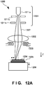
- Fig. 12A is a view explaining the configuration of a three-dimensional shaping apparatus 1200 according to the technical premise of the three-dimensional shaping apparatus 100 according to this embodiment.
- the three-dimensional shaping apparatus 1200 is an electron beam three-dimensional shaping apparatus, which shapes three-dimensional structures using an electron beam.
- the three-dimensional shaping apparatus 1200 shapes desired three-dimensional structures by melting and solidifying metal powder 1204 by the focused electron beam 1207, and sequentially laminating the metal powder.
- the three-dimensional shaping apparatus 1200 includes an electron gun 1201, a lens 1202, and a deflector 1203.
- the electron gun 1201 is a thermoelectron emission electron gun
- the lens 1202 is an electromagnetic lens
- the deflector 1203 is an electromagnetic deflector.
- the deflector 1203 consists of X-direction deflection coils and Y-direction deflection coils.
- the three-dimensional shaping apparatus 1200 further includes a mechanism (not shown) for spreading the metal powder 1204 over the shaping plane 1205, and a Z-axis stage 1206 for setting the height position of the metal powder 1204 at the height of the shaping plane 1205.
- the three-dimensional shaping apparatus 1200 spreads the metal powder 1204 over the shaping plane 1205. That is, the three-dimensional shaping apparatus 1200 forms a powder layer consisting of the metal powder 1204.
- the particle size (diameter) of the metal powder 1204 is mostly several tens of microns.
- the three-dimensional shaping apparatus 1200 causes the electron gun 1201 to generate the electron beam 1207, causes the lens 1202 to focus the electron beam 1207 so that the cross-sectional diameter of the electron beam 1207 becomes smallest on the shaping plane 1205, and causes the deflector 1203 to deflect the electron beam 1207 in two-dimensional (X and Y) directions, thereby scanning and irradiating the predetermined regions on the shaping plane 1205 with the electron beam 1207. That is, the metal powder 1204 in the region is heated. More specifically, the metal powder 1204 in the region is preheated (preliminarily sintered), and then melted.
- the deflector 1203 is controlled based on data representing the shape of the desired three-dimensional structure (shape data) and data representing shaping conditions (shaping condition data).
- shape data data representing the shape of the desired three-dimensional structure
- shaping condition data data representing shaping conditions
- the steps of preheating and melting the metal powder 1204 will hereinafter be referred to simply as the preheating and melting steps, respectively.
- the metal powder 1204 melted in the preheating and melting steps then is solidified and forms a thin metal layer as part of a desired three-dimensional structure.
- the metal layer is no longer a powder layer but is a continuous structure. Therefore, the desired three-dimensional structure is shaped by repeating the above steps of laminating such layers. Note here that this requires one to, before newly spreading the metal powder 1204 over the metal layer, compensate for the height of the structure in process by the thickness of the metal layer.
- the three-dimensional shaping apparatus 1200 moves the Z-axis stage 1206 by the thickness of the metal layer.
- the thickness that is, the moving step of the Z-axis stage 1206, in typical electron beam three-dimensional shaping apparatuses is about 100 ⁇ m. Therefore, the thickness of the powder layer consisting of the metal powder 1204 spread over the shaping plane 1205 also is about 100 ⁇ m.
- the movable range of the Z-axis stage 1206, that is, the maximum shaping depth is several hundreds of millimeters.
- the most important performance indices of the three-dimensional shaping apparatus 1200 include the shaping resolution and the shaping speed.
- the shaping resolution of the three-dimensional shaping apparatus 1200 is determined by the cross-sectional diameter of the electron beam 1207 on the shaping plane 1205.
- the shaping speed of the three-dimensional shaping apparatus 1200 is, regardless of the cross-sectional diameter of the electron beam 1207, proportional to the power of the electron beam 1207. Note that the shaping speed mentioned here does not take account of the operation of the Z-axis stage 1206.
- the shaping speed of the three-dimensional shaping apparatus 1200 is proportional to the power of the electron beam 1207 are as follows.
- the volume [cm 3 ] of a structure shaped by the three-dimensional shaping apparatus 1200 is proportional to the heat [J] given by the electron beam 1207 to the structure.
- the shaping speed [cm 3 /s] (or [cm 3 /h]) of the three-dimensional shaping apparatus 1200 is the time derivative of the volume of the structure.
- the power [W] of the electron beam 1207 is the time derivative of the heat given to the structure.
- the first reason assumes that the heat given per unit area by the electron beam 1207 to the metal powder 1204 is uniform, and the third reason assumes that the power of the electron beam 1207 is supplied to the metal powder 1204 without loss.
- the shaping speed of the three-dimensional shaping apparatus 1200 is proportional to the power of the electron beam 1207 as described above, one can increase the shaping speed by increasing the power of the electron beam 1207. However, this requires one to simultaneously increase the speed of the scan with the electron beam 1207. This is because, first, the volume is proportional to the distance of the scanning with the electron beam 1207 and, second, the time derivative of the distance is the speed of the scanning with the electron beam 1207.
- the power of the electron beam 1207 is the multiplication product of the acceleration voltage and the current of the electron beam 1207.
- the acceleration voltage of the electron beam 1207 is the voltage between the cathode 1211a and the anode 1211b in Fig. 12A .
- the acceleration voltage of the electron beam in typical electron beam three-dimensional shaping apparatuses is several tens of killovolts.
- a general way to increase the power of the electron beam 1207 is by increasing the current of the electron beam 1207.
- the current of the electron beam 1207 is controlled by adjusting the bias voltage of the electron gun 1201.
- the bias voltage is a voltage between the cathode 1211a and the grid 1211c in Fig. 12A .
- the current of the electron beam 1207 may contrarily be set small. This applies to a case in which the shaping resolution is prioritized over the shaping speed. That is, the cross-sectional diameter of the electron beam 1207 is decreased by decreasing the current of the electron beam 1207. This is because the aperture angle of the electron beam 1207 on the shaping plane 1205 decreases along with a decrease in the current of the electron beam 1207, resulting in small aberrations caused by the lens 1202. Note here that even when a high shaping resolution is required, a higher shaping speed is preferred, and thus a higher current of the electron beam 1207 is ideal.
- the control of the current by the bias voltage is also performed to completely shut off the electron beam 1207 and thereby set its current to zero.
- the process steps in which the current of the electron beam 1207 is set to zero include the step of spreading the metal powder 1204 over the shaping plane 1205 and the step of moving the Z-axis stage 1206.
- the shaping speed of the three-dimensional shaping apparatus 1200 being high means that the time during which each point in the region scanned with the electron beam 1207 is irradiated is short.
- the time mentioned here is the quotient of the cross-sectional diameter of the electron beam 1207 divided by the speed of the scanning with the electron beam 1207, and is also the quotient of the heat given per unit area to the metal powder 1204 divided by the power of the electron beam 1207 per unit area. That is, the time during which each point in the region scanned with the electron beam 1207 is irradiated is inversely proportional to the speed of the scanning with the electron beam 1207 and is proportional to the heat given per unit area to the metal powder 1204.
- the above heat per unit area is, in the preheating step, heat required per unit area to raise the temperature of the metal powder 1204 from an initial temperature to a preheating temperature, and is also, in the melting step, the sum of heat required per unit area to raise the temperature of the metal powder 1204 from the preheating temperature to a target temperature and heat required per unit area to melt the metal powder 1204.
- melting of the metal powder 1204 refers to that the metal powder 1204 melts as a result of its absorbing the melting heat (latent heat) at its melting point.
- the above power per unit area is also the quotient of the power of the electron beam 1207 divided by the cross-sectional area of the electron beam 1207. Therefore, the power per unit area increases when the power of the electron beam 1207 is increased to increase the shaping speed, when the cross-sectional diameter of the electron beam 1207 is decreased to increase the shaping resolution, or when the power of the electron beam 1207 is increased and the cross-sectional diameter of the electron beam 1207 is decreased to increase both the shaping speed and the shaping resolution.
- the heat given per unit area by the electron beam 1207 to the metal powder 1204 increases or decreases depending on the speed of the scanning with the electron beam 1207. Therefore, whether or not to melt the metal powder 1204 can be controlled by the scanning speed. That is, the metal powder 1204 melts when the scanning speed is decreased, but does not melt when the scanning speed is increased.
- the above fact is an advantage in the melting step. This is because the scans of regions where the metal powder 1204 is melted include, unless the entire scan of the regions to be scanned altogether can be a single continuous scan, scans of regions where the metal powder 1204 is not melted. That is, in the melting step, the metal powder 1204 in the region where the metal powder 1204 is not supposed to be melted can be given nonzero heat per unit area, which heat can lead to unnecessary melting of the metal powder 1204, but such unnecessary melting can be prevented by setting the scanning speed for the region where the metal powder 1204 is not supposed to be melted to be higher than that for the region where the metal powder 1204 is melted.
- the unnecessary melting can be theoretically prevented by the current control of the electron beam 1207, which control is by changing the bias voltage, or by blanking of the electron beam 1207.
- control is difficult in most cases.
- the reason why the current control of the electron beam 1207 by changing the bias voltage is difficult is that it is difficult to change the bias voltage at a high speed because the bias voltage is generally as high as several kilovolts. If it takes a long time to change the current for the above reason, the shaping speed decreases. Compared with the change in the current, the change in the scanning speed can be made extremely fast.
- the reason why the blanking of the electron beam 1207 is difficult is that the current of the electron beam 1207 is high enough to melt metal objects, and thus deflecting the electron beam 1207, even if temporarily, to make it incident on a shielding plate (metal) or the like can cause thermal damage to it and its surroundings.
- the preheating and melting of the powder layer consisting of the metal powder 1204 are not completed only by scanning and irradiating the powder layer with the electron beam 1207. More specifically, the preheating and melting of the powder layer require that heat given by the scanning and irradiation of the powder layer to the heat generating part (superficial part) of the powder layer be diffused to a deeper part of the powder layer. This is because in most cases the thickness of the heat generating part is smaller than that of the powder layer.
- the thickness of the heat generating part is several microns to several tens of microns when the acceleration voltage of the electron beam 1207 is several tens of kilovolts. In contrast, the thickness of the powder layer is about 100 ⁇ m, as described above.
- the preheating and melting of the powder layer requiring the thermal diffusion can prevent one from increasing the power of the electron beam 1207 per unit area to improve the shaping speed, resolution, or both of the three-dimensional shaping apparatus 1200. This depends on the relationship between the time during which each point scanned with the electron beam 1207 is irradiated and the time taken for the thermal diffusion. If the former time is shorter than the latter time, that is, if the power of the electron beam 1207 per unit area is accordingly increased, the heat given to the superficial part of the powder layer can, without waiting for the thermal diffusion, melt and evaporate only the superficial part and its vicinity.
- the metal powder 1204 can evaporate regardless of whether or not its temperature exceeds its melting point. More specifically, the evaporation amount increases exponentially with respect to rising temperature. The evaporation cannot be avoided as long as the metal powder 1204 is heated. If the evaporation amount is excessive, the following problems become conspicuous.
- the thickness of the metal layer formed by the melting and solidification of the metal powder 1204 decreases.
- an evaporated metal film is formed on the inner wall of the three-dimensional shaping apparatus 1200, and thus its inside becomes contaminated. The increase in the thickness of the film increases the ease with which it flakes off, and when it flakes off, it prevents the metal powder 1204 beneath it from being irradiated and heated as expected.
- FIG. 12B is a flowchart explaining the procedure of shaping a three-dimensional structure with the three-dimensional shaping apparatus 1200.
- step S1201 the three-dimensional shaping apparatus 1200 loads the shape data and shaping condition data for one powder layer.
- step S1203 the three-dimensional shaping apparatus 1200 spreads the metal powder 1204 over the shaping plane 1205, thereby forming a powder layer consisting of the metal powder 1204.
- step S1205 to preheat the metal powder 1204 in a predetermined region (or the entire region) on the shaping plane 1205, the three-dimensional shaping apparatus 1200 scans and irradiates the region by causing the main deflector 1203 to deflect the electron beam 1207.
- step S1207 to melt the metal powder 1204 in the predetermined region, the three-dimensional shaping apparatus 1200 scans and irradiates the predetermined region by causing the main deflector 1203 to deflect the electron beam 1207.
- step S1209 the three-dimensional shaping apparatus 1200 judges whether or not the scanning and irradiation has been completed for all layers. If the judgment is that the scanning and irradiation has been completed (YES in step S1209), the three-dimensional shaping apparatus 1200 ends shaping; otherwise (NO in step S1209), the three-dimensional shaping apparatus 1200 advances to step S 1211.
- step S 1211 the three-dimensional shaping apparatus 1200 moves the Z-axis stage 1206 by the thickness of the metal layer formed in the above steps. The three-dimensional shaping apparatus 1200 repeats step S1201 and the subsequent steps.
- Fig. 1 is a view explaining the configuration of the three-dimensional shaping apparatus 100 according to this embodiment.
- the three-dimensional shaping apparatus 100 basically has the same configuration as that of the three-dimensional shaping apparatus 1200 shown in Fig. 12A . That is, as shown in Fig. 1 , the three-dimensional shaping apparatus 100 includes an electron gun 101, a lens 102, a deflector 103, and a Z-axis stage 106.
- the deflection area that is, the shaping area of the main deflector 103 of the three-dimensional shaping apparatus 100, is a 200-mm square.
- the movable range of the Z-axis stage 106 of the three-dimensional shaping apparatus 100 that is, the maximum shaping depth, is 200 mm.
- the configuration of the three-dimensional shaping apparatus 100 is different from that of the three-dimensional shaping apparatus 1200 shown in Fig. 1 in that the former, unlike the latter, includes a sub-deflector 108 as a deflector in addition to the main deflector 103.
- the sub-deflector 108 consists of X-direction deflection coils and Y-direction deflection coils.
- the deflection area of the sub-deflector 108 is square and has a size of 4 mm square, which is much smaller than the size of the deflection area of the main deflector 103.
- the reason why the deflection area of the sub-deflector 108 is as small as described above is that the number of turns for the coils forming the sub-deflector 108 is smaller than that for the coils forming the main deflector 103.
- the deflection area of the sub-deflector 108 will hereinafter be referred to as the sub-deflection field.
- the three-dimensional shaping apparatus 100 includes, as components of the control system, a central controller 110, a bias voltage controller 111, a sub-deflection controller 112, a main deflection controller 113, a stage controller 114, and a storage unit 120.
- the bias voltage controller 111 is connected to the grid 101c, the sub-deflection controller 112 is connected to the sub-deflector 108, the main deflection controller 113 is connected to the main deflector 103, and the stage controller 114 is connected to the Z-axis stage 106.
- the bias voltage controller 111, sub-deflection controller 112, main deflection controller 113, and stage controller 114 each are also connected to the central controller 110.
- the central controller 110 is connected to the storage unit 120.
- the storage unit 120 stores shape data and shaping condition data.
- the operation of the three-dimensional shaping apparatus 100 is basically the same as that of the three-dimensional shaping apparatus 1200 shown in Fig. 12A . That is, as with the three-dimensional shaping apparatus 1200 shown in Fig. 12A , the three-dimensional shaping apparatus 100 spreads metal powder 104 over the shaping plane 105, thereby forming a powder layer consisting of the metal powder 104.
- the three-dimensional shaping apparatus 100 causes the electron gun 101 to generate an electron beam 107, causes the lens 102 to focus the electron beam 107, causes the main deflector 103 to deflect the electron beam 107, and scans and irradiates the metal powder 104 with the electron beam 107, thereby preheating (preliminarily sintering) the metal powder 104, and melting and solidifying the metal powder 104.
- the three-dimensional shaping apparatus 100 uses the Z-axis stage 106 to compensate for an increase in the height of a three-dimensional structure in process, which increase results from the melting and solidification of the metal powder 104.
- the operation of the three-dimensional shaping apparatus 100 is different from that of the three-dimensional shaping apparatus 1200 shown in Fig. 12A in that unlike the latter the former uses, in the melting step, the sub-deflector 108 in addition to the main deflector 103 to scan and irradiate the metal powder 104, and performs, in the melting step, multiple scanning and irradiation of regions where the metal powder 104 is melted.
- the three-dimensional shaping apparatus 100 uses the sub-deflector 108 to scan not only the regions where the metal powder 104 is melted but also the regions where the metal powder 104 is not melted, the scanning of the latter regions preventing unnecessary melting of the metal powder 104 in them.
- the reason why the three-dimensional shaping apparatus 100 uses the sub-deflector 108 to scan and irradiate the metal powder 104 in the melting step is to increase, in the melting step, the scanning speed of when performing multiple scanning and irradiation of the regions where the metal powder 104 is melted and the scanning speed of when scanning, while preventing the unnecessary melting, the regions where the metal powder 104 is not melted. That is, the scanning speed of the sub-deflector 108 is higher than that of the main deflector 103. This is ensured by the response speed of the sub-deflector 108 and sub-deflection controller 112 being higher than that of the main deflector 103 and main deflection controller 113.
- the high response speed stems from the fact that the number of turns for the coils forming the sub-deflector 108 is smaller than that of the coils forming the main deflector 103, that is, the fact that the inductance of the former is smaller than that of the latter.
- the reason why the three-dimensional shaping apparatus 100 performs, in the melting step, multiple, not single, scanning and irradiation of the regions where the metal powder 104 is melted is to, in the melting step, reduce the heat given per unit area to the powder layer consisting of the metal powder 104, and diffuse the heat given to the heat generating part (superficial part) to a deeper part of the powder layer gradually. This can prevent the excessive temperature rise of the metal powder 104, thereby preventing excessive evaporation of the metal powder 104. Note that implementing this makes it necessary to increase the scanning speed for the region. That is, the high-speed response of the sub-deflector 108 and sub-deflection controller 112 is an advantage for the scanning.
- the operations of the controllers 110, 111, 112, 113, and 114 of the three-dimensional shaping apparatus 100 are as follows.
- the data stored in the storage unit 120 is input to the central controller 110.
- the central controller 110 controls the bias voltage controller 111, main deflection controller 113, sub-deflection controller 112, and stage controller 114. More specifically, the central controller 110 increases or decreases the current of the electron beam 107 by changing the bias voltage via the bias voltage controller 111, operates the main deflector 103 via the main deflection controller 113, and operates the sub-deflector 108 via the sub-deflection controller 112, and moves the Z-axis stage 106 by a necessary moving step via the stage controller 114.
- the storage unit 120 stores the following as shaping conditions: the acceleration voltage and current of the electron beam 107, the density [g/cm 3 ], specific heat [J/(g ⁇ K)], heat conductivity [W/(cm ⁇ K)], melting heat [J/g], room temperature [°C], preheating temperature [°C], and target temperature [°C] of the metal powder 104, and the thickness [ ⁇ m] of the powder layer consisting of the metal powder 104, as well as the degree of multiplication of the scanning and irradiation, that is, the repetition number of the scanning.
- the room temperature, preheating temperature, and target temperature determine the temperature rises of the powder layer consisting of the metal powder 104 in the preheating and melting steps, and the room temperature, preheating temperature, target temperature, and the density, specific heat, and melting heat of the metal powder 104 determine the heats to be given per unit volume [J/cm 3 ] to the powder layer in the preheating and melting steps.
- the above temperature rises and heats per unit volume are those of when the temperature distribution of the powder layer consisting of the metal powder 104 in the depth direction (Z direction) is leveled.
- Multiplying the heats per unit volume by the thickness of the powder layer consisting of the metal powder 104 gives the heats given per unit area [J/cm 2 ] to the powder layer in the preheating and melting steps.
- Dividing the heats per unit area by the power of the electron beam 107 per unit area [W/cm 2 ] gives the times [t] during which each point in the regions where the metal powder 104 is melted is irradiated in the preheating and melting steps, and dividing the times by the repetition number of the scanning gives the irradiation time [t] per irradiation for each point.
- the above power of the electron beam 107 per unit area is determined by the acceleration voltage, current, and cross-sectional diameter of the electron beam 107. Further dividing the distance between two adjacent points in the region by the irradiation time per irradiation gives the speed of the scanning of the region with the electron beam 107. These calculations are performed by the central controller 110.
- the melting step according to this embodiment will be described in detail below.
- the preheating step according to this embodiment is the same as that in conventional techniques and a description thereof will be omitted.
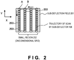
- Fig. 2 is a view explaining how a small region in the sub-deflection field is scanned and irradiated with the electron beam by the three-dimensional shaping apparatus according to this embodiment.
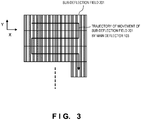
- Fig. 3 is a view explaining how small regions to be scanned and irradiated by the three-dimensional shaping apparatus according to this embodiment are arranged on the shaping plane.
- the small region shown in Fig. 2 is identical to each of the small regions shown in Fig. 3 .
- the scanning and irradiation is performed by dividing the region where the metal powder 104 is melted into small regions 202 each of which can be included in the deflection field of the sub-deflector 108, that is, the sub-deflection field 201, causing the sub-deflector 108 to perform multiple scanning of each small region 202, and causing the main deflector 103 to shift the sub-deflection field every time the scanning of one small region 202 is completed.
- the small regions 202 completed with the multiple scanning and irradiation by the sub-deflector 108 are arranged successively on the shaping plane 105 and the regions where the metal powder 104 is melted are filled with the small regions.
- the completion of the scanning of one small region 202 refers to that as a result of the multiple scanning and irradiation of the small region 202, all points in it are given heat necessary to melt the metal powder 104.
- the region where the metal powder 104 is melted is small, and can thus be included in the sub-deflection field 201, the region need not be divided into smaller regions. In that case, the region can be processed as one small region 202.
- the small regions 202 included in the sub-deflection field 201 in this embodiment each form a one-dimensional grid.
- the one-dimensional grid is a division of a one-dimensional grid larger than the sub-deflection field 201, which grid is divided into grids each having a size equal to that of the sub-deflection field 201. Note that when a plurality of the one-dimensional grids are laminated, their directions are rotated by 90° one layer after another. This connects X-direction one-dimensional grids and Y-direction one-dimensional grids in the Z direction, thereby forming one continuous, self-standing structure.
- the trajectories indicated by the solid and the dotted lines are those of the scanning by the sub-deflector 108 in the region where the metal powder 104 is melted (small region 202) and the region where the metal powder 104 is not melted, respectively.
- Each circle 203 on the trajectory indicated by the solid lines is a circle centered at each point irradiated with the electron beam 107, and represents the cross section of the electron beam 107. That is, each circle 203 is the smallest component of the small region 202.
- the start and the end point of the scanning (one separate scanning) of the small region 202 are points A and B in Fig. 2 , respectively.
- the scanning starts at point A.
- point B the same scanning starts again from point A unless the repetition number of the scanning reaches a predetermined number.
- the electron beam 107 irradiates somewhere in the small region 202, but none of the points in it is irradiated continuously with the electron beam 107. More specifically, any arbitrary point is given a very short time of irradiation periodically. That is, the nth irradiation of any arbitrary point starts after a predetermined waiting time after the (n-1)th irradiation of that point is completed, where n is a natural number which can take all integer values equal to or larger than 2.
- the points other than the above arbitrary point are scanned and irradiated. More specifically, assuming that the arbitrary point is a point given the mth irradiation among all the points in the small region 202, the other points in the small region 202, during the waiting time, are irradiated in the following manner: the points given the (m+1)th, (m+2)th,..., Mth irradiation in the sub-deflection field 201 are each given the (n-1)th round of irradiation, and the points given the first, second,..., (m-1)th irradiation in the sub-deflection field 201 are each given the nth round of irradiation.
- the three-dimensional shaping apparatus 100 does not wait still but scans the region where the metal powder 104 is melted, and advances the melting of the metal powder 104 in the region.
- t w be the waiting time
- t e be an irradiation time necessary to melt the metal powder 104 at the arbitrary point.
- N ( ⁇ 2) is the maximum value of n, and represents the total repetition number of the scanning, that is, the number of division of the irradiation time at each point in the small region 202
- t s represents the time which is included in the waiting time t w and which is taken to scan the region which is included in the sub-deflection field 201 and where the metal powder 104 is not melted.
- the time which is included in the waiting time t w and which is taken to scan and irradiate the region which is included in the sub-deflection field 201 and where the metal powder 104 is melted is represented by the first term on the right-hand side of equation (1), that is, (t e /N)(M - 1). This is the sum of the irradiation time per irradiation of the arbitrary point, that is, t e /N, over the (M-1) points in total.
- the waiting time t w is set to a value equal to or longer than a predetermined time based on the thickness and thermal diffusion coefficient of the powder layer consisting of the metal powder 104. That is, let t d be the predetermined time, and then the relationship between t d and t w is defined as: t w ⁇ t d Equation (1) and inequality (2) give a relationship of: t e / N M ⁇ 1 + t s ⁇ t d The predetermined time t d will be described later.
- N and M to be such that they satisfy inequality (3), one can, in the above operation, prevent the excessive temperature rise of the metal powder 104 in the small region 202 and thus prevent the excessive evaporation of the metal powder 104.
- the irradiation, the (n-1)th or nth, of the other points progresses, and thus no overhead time is generated. That is, the shaping speed does not deteriorate.
- the result may be that the superficial part of the powder layer in the small region 202 is melted but a deeper part remains unmelted. This can be coped with by giving a margin to the target temperature or the irradiation time t e , as will be described later.
- T(z, t) is a solution under the condition that the outermost and deepest parts of the powder layer are thermally insulated, that is, under the condition that the temperature gradient ⁇ T(z, t)/ ⁇ z is zero at the outermost and deepest parts of the powder layer, and represents, for the sake of convenience, a temperature change of the powder layer as a result of an arbitrary round of irradiation. That is, without the arbitrary round of irradiation, T(z, t) is zero.
- T 0 z t a 0
- Equation (6) is the total sum of the second- and higher-order components of T(z, t). Descriptions of the coefficients of these components will be omitted for brevity.
- the other components that is, the first-order component T 1 (z, t) and the second- and higher-order components, attenuate with time, and are not necessary to melt the powder layer.
- the heat given to the heat generating part of the powder layer being sufficiently diffused to a deeper part of the powder layer, that is, T(z, t) sufficiently approaching a 0 corresponds to the first- and higher-order components of T(z, t) becoming sufficiently small with time, as compared with the zeroth-order component T 0 (z, t) of T(z, t).
- Whether the first-order component T 1 (z, t) has sufficiently attenuated at an arbitrary time can be judged from whether
- at the depth position z 0 or L, that is,
- a 0 .
- T 1 (0, t) sufficiently small with respect to T 0 (0, t)
- T w ⁇ t d
- ⁇ which is equal to or greater than 1, represents a factor by which to extend t w . This factor will hereinafter be referred to as the extension factor.
- T(z, t) may be closer to the zeroth-order component a 0 but may never be farther away from it, and thus no problem is caused to the operation of the three-dimensional shaping apparatus 100.
- the temperature distribution of the powder layer irradiated with the electron beam 107in the depth direction (Z direction) and the time transition of its temperature distribution were investigated by numerical thermal analysis for the different numbers of division N of the irradiation time and different waiting times t w . The method and the results of the analyses, and discussion of the results will be described below.
- T(z, t) represents the temperature [°C] of the powder layer at an arbitrary point in the small region 202. That is, T(z, t) does not represent a temperature change of the powder layer due to an arbitrary round of irradiation, and thus does not become zero even without the arbitrary round of irradiation.
- Q(z, t) represents the heat per unit volume [W/cm 3 ] at an arbitrary point in the small region 202, and takes a nonzero value while the point is irradiated with the electron beam 107, but is zero otherwise.
- These functions both assume the time t to be zero at the time point where the first round of the total of N times of irradiation with the electron beam 107 starts.
- N is 2 or greater as long as the small region 202 undergoes the multiple scanning and irradiation, but is 1 otherwise.
- Fig. 4 shows a calculation model for the analysis.
- the model assumes the following conditions.
- the powder layer consisting of the metal powder 104 is a continuous layered material 401 regardless of the gaps between the particles of the metal powder 104, and the density, specific heat, and heat conductivity of the layered material 401 are uniform. These values are constant regardless of melting or solidification of the layered material 401.
- the heat in the heat generating part 411a of the layered material 401 is also uniform.
- the power given per unit area by scanning the layered material 401 to the layered material 401 is determined by simply dividing the power of the electron beam 107 by its cross-sectional area.
- the power of the electron beam 107 is supplied to the heat generating part 411a without loss.
- the outer side of the heat generating part 411 a coincides with the outermost part 411b, and the thickness of the heat generating part 411a is smaller than that of the layered material 401.
- the layered material 401 is thermally continuous in the range from the outermost part 411b to the deepest part 411c and thus heat can be diffused in the range, but the layered material 401 is thermally insulated at the outermost part 411b and deepest part 411c and thus the heat is not diffused to above the outermost part 411b or to below the deepest part 411c.
- the boundary condition for the solutions of equation (13) is that the gradients of the solutions at the boundaries, that is, the temperature gradients ⁇ T(0, t)/ ⁇ z and ⁇ T(L, t)/ ⁇ z, are zero.
- the temperature of the layered material 401 before irradiation with the electron beam 107 is uniform, and is equal to the preheating temperature of the metal powder 104.
- the superficial part of the layered material 401 is continuously irradiated with the electron beam 107 regardless of the temperature rise.
- the temperature of the superficial part of the powder layer consisting of the metal powder 104 rises and thus the outer side of the powder layer is evaporated, the outermost part of the powder layer shifts toward the deeper side.
- the powder layer is given, at each point of irradiation, a recess having a diameter almost equal to that of the electron beam 107.
- the acceleration voltage of the electron beam 107 was set to 50 kV, and the current of the electron beam 107 was set to 0.10, 1.0, or 10 mA.
- the cross-sectional diameter of the electron beam 107 on the shaping plane 105 was set to 0.2 mm regardless of the current of the electron beam 107. From these values, the power of the electron beam 107 was determined to be 0.0050, 0.050, or 0.50 kW, and the power of the electron beam 107 per unit area was determined to be 0.016, 0.16, or 1.6 MW/cm 2 .
- the thickness of the layered material 401 was set to 50 ⁇ m, and the thickness of the heat generating part 411a (superficial part) of the layered material 401 was set to 10 ⁇ m. From the thickness of the heat generating part 411 a and the power per unit area, the heat per unit volume Q in the heat generating part 411a of the layered material 401 was determined to be 1.6 GW/cm 3 .
- the material for the layered material 401 was chosen to be titanium (Ti), and the heat conductivity ⁇ , density ⁇ , and specific heat c of Ti was set to 0.17 W/(cm ⁇ K), 4.5 g/cm 3 , and 0.52 J/(g ⁇ K), respectively.
- the thermal diffusion coefficient ⁇ of Ti was determined to be 0.073 cm 2 /s.
- the predetermined time t d was determined to be 35 ⁇ s.
- the melting point and melting heat of Ti were chosen to be 1,668°C and 0.30 kJ/g, respectively.
- the density ⁇ of the powder layer consisting of the metal powder 104 decreases accordingly.
- the power given per unit area to the powder layer decreases by the energy of the electrons reflected by the powder layer, and thus the heat per unit volume Q decreases accordingly.
- the heat per unit volume Q can further decrease because of the gaps between the particles of the metal powder 104. This is because the gaps increase the amount of electrons which pass per unit area through the powder layer increases, and the power given per unit area to the powder layer decreases accordingly.
- the preheating temperature and target temperature of the layered material 401 were set to 800°C and 1,768°C, respectively. From these temperatures and the above thickness and physical properties, it follows that the heat necessary per unit area to raise the temperature of the layered material 401 from the preheating temperature to the target temperature, the heat necessary per unit area to melt the layered material 401, and the sum of these heats are 11, 6.8, and 18 J/cm 2 , respectively.
- the target temperature is the sum of the melting point of Ti, 1,668°C, and a temperature margin of 100°C.
- the above margin is effective also in cancelling heat shortages due to such errors as errors in the thickness of the powder layer consisting of the metal powder 104, errors in the measurements of the beam current, and errors of the measurements of the beam cross-sectional diameter, and, in addition, a heat shortage caused by the heat dissipation, which is due to the evaporation of the superficial part of the powder layer.
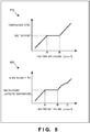
- 510 is a graph showing the relationship between the temperature T [°C] at an arbitrary depth position of the layered material 401 and the heat per unit volume [J/cm 3 ] at the position.
- points A and B respectively represent the start and the end point of the melting of the layered material 401 at the position.
- the width of the region is equal to the heat per unit volume necessary to melt the layered material 401, that is, the product of the melting heat [J/g] and the density [g/cm 3 ] of the layered material 401.
- the characteristic that the temperature T remains at the melting point in the above region can be seen not only in pure metals (Ti in this embodiment) but also in alloys.
- a relationship similar to the above but with the layered material 401 being an alloy is shown in 520 of Fig. 5 .
- the consideration of the melting and solidification refers to providing the routine of solving equation (13) with a series of processes of evaluating the heat of the layered material 401 per unit volume, and modifying the temperature T(z, t) in accordance with the evaluation result. More specifically, the series of processes first determines the heat accumulated per unit volume in a microvolume at each depth position z at time t and, second, sets T(z, t) to that determined from equation (13) if the heat per unit volume is not in the range from point A to B, but resets T(z, t) to the melting point of the layered material 401 if the heat per unit volume is in the range from point A to B.
- the temperature distribution of the layered material 401 in the depth direction (Z direction) was calculated by solving equation (13). For this, the number of division N of the irradiation time was set to 1 (not multiple irradiation) and the current of the electron beam 107 was set to 0.10, 1.0, or 10 mA. The results are shown in Fig. 6 .
- the temperature distribution s shown in Fig. 6 are those at the completion of the irradiation operation with the electron beam 107.
- the broken line in Fig. 6 locates 1,668°C, that is, the melting point of the layered material 401 (Ti). Likewise the broken lines in similar figures below locate the melting point of the layered material 401 or other materials.
- the heat given per unit area to the layered material 401 to obtain the above temperature distributions was, regardless of the current of the electron beam 107, set to 18 J/cm 2 , that is, the above-mentioned summed heat per unit area. From the summed heat values per unit area for the above three current values, that is, 0.016, 0.16, and 1.6 MW/cm 2 , the irradiation times t e for each point in the small region 202 for the three current values were respectively 1.1 ms, 0.11 ms, and 11 ⁇ s.
- the irradiation time t e for each point is longer than the predetermined time t d (35 ⁇ s) if the current of the electron beam 107 is 0.10 or 1.0 mA, but is shorter than the predetermined time if the current is 10 mA. From these irradiation times t e and the cross-sectional diameter of the electron beam 107, that is, 0.2 mm, the scanning speeds determined for the three current values were 0.18, 1.8, and 18 m/s, respectively.
- the temperature of the outermost part 411b at the completion of the irradiation with the electron beam 107 for its current of 0.10, 1.0, or 10 mA is about 2,000°C, 3,100°C, or 6,200°C, respectively.
- the current of the electron beam 107 is 0.10 or 1.0 mA, that is, if the irradiation time t e (1.1 or 0.11 ms) for each point in the small region 202 is longer than the predetermined time t d (35 ⁇ s), the temperature of the outermost part 411b is relatively close to the melting point (1,668°C) of the layered material 401.
- the temperature of the outermost part 411b is significantly higher than the melting point of the layered material 401.
- the temperature of the deepest part 411c at the same time point is, for the current of 0.10 mA, equal to the melting point of the layered material 401; for the current of 1.0 mA, slightly lower than the melting point; for the current of 10 mA, about 800°C, which hardly shows any increase from the preheating temperature (800°C) of the layered material 401.
- the temperature of the outermost part 411b being very high but that of the deepest part 411c remaining low, as described above, for the current of the electron beam 107 of 10 mA means that at the completion of the irradiation operation of the layered material 401 with the electron beam 107, the heat given by the electron beam 107 to the superficial part (heat generating part 411a) of the layered material 401 is yet to be transferred to a deeper part of the layered material 401 sufficiently and remains in the superficial part and its vicinity of the layered material 401.
- a deeper part of the layered material 401 is yet to absorb the melting heat, and therefore the heat remaining in the superficial part and its vicinity of the layered material 401 includes the heat that should finally be absorbed by a deeper part of the layered material 401 as the melting heat. That is, the temperature of the superficial part of the layered material 401 is high accordingly.
- the temperature of the deepest part 411c at the completion of the irradiation with the electron beam 107 being equal to the melting point of the layered material 401, as described above, for the current of the electron beam 107 of 0.10 mA is due to the relationship shown in 510 of Fig. 5 . That is, at that time point, the heat per unit volume at the deepest part 411c exists in the range from point A to B in 510 of Fig. 5 , and thus the temperature of the deepest part 411c remains at the melting point of the layered material 401.
- the temperature of the layered material 401 irradiated with the electron beam 107 becomes highest or lowest in the outermost part 411b or the deepest part 411 c, respectively. This is because the temperature gradient ⁇ T(z, t)/ ⁇ z becomes zero in the outermost part 411b and deepest part 411c, and because the outer side of the heat generating part 411 a coincides with the outermost part 411b.
- the highest reached temperature of the layered material 401 is identical to that of the outermost part 411b and the completion of the melting of the layered material 401 is equivalent to the melting of the deepest part 411c.
- the melting of the deepest part 411c corresponds to the heat per unit volume at it exceeding point B in 510 of Fig. 5 .
- the current of the electron beam 107 was set to the largest of the above three current values, that is, 10 mA, and the cross-sectional diameter of the electron beam 107 was set to 0.2 mm, as designated above.
- Fig. 7 shows the time transitions of the temperatures of the outermost part 411b and deepest part 411c obtained by setting the current and cross-sectional diameter of the electron beam 107 to the above values, and setting the number of division N of the irradiation time to 1 (not multiple irradiation).
- the peak value of the temperature of the outermost part 411b shown in Fig. 7 is equal to the above-described highest reached temperature, that is, about 6,200°C ( Fig. 6 ).
- the highest reached temperature of the outermost part 411b is the temperature of the outermost part 411b at the completion of the irradiation with the electron beam 107.
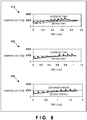
- Fig. 8 shows the time transitions of the temperatures of the outermost part 411b and deepest part 411c obtained by setting the current and cross-sectional diameter of the electron beam 107 again to the above values, but setting the number of division N of the irradiation time to 10 (multiple irradiation).
- the irradiation time per irradiation t e /N and the speed of the scanning with the electron beam 107 are 1.1 ⁇ s and 0.18 km/s, respectively, regardless of the waiting time t w .
- the total number M of the points in the small region 202 are determined from equation (1) to be 32, 93, and 164, respectively. Note that here the speed of the scanning of the region which is included in the sub-deflection field 201 and where the metal powder 104 is not melted is considered sufficiently high and the distance of the scanning is considered sufficiently short, and thus the time t s taken to scan the region where the metal powder 104 is not melted is ignored.
- the area ratio of the small region 202 that is, the one-dimensional grid shown in Fig. 2 to the sub-deflection field 201 is 0.5
- the highest reached temperature (about 2,500°C) of the layered material 401 of when the waiting time t w is 105 or 185 ⁇ s being lower than the highest reached temperature (about 2,800°C) of when t w is 35 ⁇ s, as described above, is because when t w is 105 or 185 ⁇ s, the heat given to the heat generating part (superficial part) of the layered material 401 is diffused toward a deeper part of the layered material 401 more thoroughly than when t w is 35 ⁇ s. This is found from the fact that, as shown in 820 and 830 of Fig.
- the highest reached temperature of the layered material 401 of when the waiting time t w is 105 or 185 ⁇ s is almost equal to the sum of the melting point of the layered material 401 and the maximum temperature rise per irradiation, as is found from 820 and 830 of Fig. 8 .
- the temperature of the outermost part 411b immediately before the start of the irradiation that raises the temperature to the highest reached temperature, that is, the Nth round of irradiation is at or near the melting point of the layered material 401.
- the maximum temperature rise per irradiation refers to a temperature rise in the region on the right-hand side of point B in Fig. 5 , that is, a temperature rise which is not influenced by the nonlinearity of the temperature T.
- the reasons why the temperature of the outermost part 411b immediately before the start of the Nth round of irradiation is at or near the melting point of the layered material 401 are as follows. First, as long as the waiting time t w satisfies inequality (2), the heat in the layered material 401 is sufficiently diffused in the depth direction (Z direction) during the waiting time t w , and thus the temperature distribution of the layered material 401 is leveled.
- the target temperature (1,768°C) of the layered material 401 is higher than the melting point (1,668°C) of the layered material 401, but the excess is as small as the above margin (100°C), and thus, when the temperature distribution becomes leveled, the temperature of the outermost part 411b cannot be significantly higher than the melting point of the material.
- the temperature of the outermost part 411b immediately before the start of the Nth round of irradiation cannot exceed the melting point of the layered material 401 significantly. This is because if the heat given per unit area to the layered material 401 becomes sufficient and the deepest part 411c is melted, that is, if the temperature of the deepest part 411c exceeds the melting point of the layered material 401, the deepest part 411c becomes thermally coupled to the powder layer or metal layer beneath it, and is thus cooled, and therefore the temperature rise of the outermost part 411b is suppressed.
- the highest reached temperature (about 2,500°C) can be further lowered by increasing the number of division N of the irradiation time, which increase shortens the irradiation time per irradiation t e /N. This is because if the irradiation time per irradiation t e /N is sufficiently shorter than the predetermined time t d , the thermal diffusion in the layered material 401 during the irradiation time per irradiation t e /N can be ignored, and thus the temperature rise of the heat generating part of the layered material 401 can be considered proportional to the heat given per unit area to the layered material 401, that is, proportional to t e /N.
- N is increased, one needs, because of the resulting shortening of t e /N, to increase the speed of the scanning by the sub-deflector 108. Furthermore, one needs, in order to satisfy inequality (3), to increase the total number of points M in the sub-deflection field 201. That is, increasing N makes it necessary to increase the response speed of the sub-deflector 108 and sub-deflection controller 112, and simultaneously extend the sub-deflection field 201.
- the response speed of the sub-deflector 108 and sub-deflection controller 112 cannot be increased unlimitedly. That is, the number of division N of the irradiation time is limited by the response speed of the sub-deflector 108 and sub-deflection controller 112. Furthermore, it is difficult to keep the response speed high and simultaneously increase the sub-deflection field 201. This is because the response speed and the size of the sub-deflection field 201 are given restrictions associated with electric circuits.
- extending the sub-deflection field 201 makes it necessary to increase the number of turns of the coils forming the sub-deflector 108, increase the current flowing through the coils, or take both these measures.
- increasing the number of turns of the coils delays the responses of the coils, and also makes it necessary to increase the rated voltage of the amplifiers used. That is, a difficulty arises of increasing both the rated voltage and the operating speed.
- increasing the current flowing through the coils increases the heat generated by the amplifiers, and thus results in instability in the circuit operation. That is, a difficulty arises of increasing both the rated current and the current accuracy.
- the reason why increasing the number of turns of the coils makes it necessary to increase the rated voltage of the amplifiers is that the voltages across the coils increase with the increase in the inductances.
- the powder layer consisting of the metal powder 104 was a single continuous layered material 401, which was thermally insulated at the outermost part 411b and deepest part 411 c, and that the layered material 401 was thermally continuous in the range from the outermost part 411b to the deepest part 411c.
- a powder layer consisting of the metal powder 104 can have, in the range from the outermost to the deepest part, a thermally discontinuous plane.
- the reasons for this are as follows. First, as long as the particle size of the metal powder 104 is smaller than the thickness of the powder layer consisting of the metal powder 104, the thickness of the powder layer can contain a plurality of particles of the metal powder 104. Second, there are gaps between the plurality of particles of the metal powder 104. Third, the contact between particles of the metal powder 104 is a point contact, resulting in poor heat conduction. These explanations are illustrated by Fig. 9 .
- the particle size of the metal powder 104 is necessarily and obviously equal to or smaller than the thickness of the powder layer consisting of the metal powder 104. Moreover, the particle size of the metal powder 104 generally is not uniform and has a certain dispersion. For these reasons, the thickness of the powder layer can always contain a plurality of particles of the metal powder 104. That is, the metal powder 104 being spread over the shaping plane 105 is a result of relatively large powder particles forming gaps within the thickness of the powder layer consisting of the metal powder 104, and relatively small powder particles filling the gaps. Consequently, the powder layer has a discontinuous plane such as described above without exception.
- the depth position of the discontinuous plane that is, the depth position of one or some of the gaps depends on the size relationship between the plurality of particles, as is apparent from Fig. 9 . That is, the depth position has a dispersion that stems from the dispersion in the particle size of the metal powder 104.
- the discontinuous plane impedes the thermal diffusion from the superficial to a deeper part of the powder layer consisting of the metal powder 104. Therefore, the temperature distribution of the powder layer consisting of the metal powder 104 and the time transition of its temperature distribution may actually be different from those of the layered material 401.
- the discontinuous plane 911d was assumed to be perpendicular to the depth direction (Z direction), as shown in 910 of Fig. 9
- the layered material 901 was assumed to be thermally continuous in the range from the outermost part 911b to the discontinuous plane 911d and in the range from the discontinuous plane 911d to the deepest part 911c.
- the discontinuous plane 911d was assumed to turn to a thermally continuous plane along with the melting of the layered material 901 in the range from the outermost part 911b to the discontinuous plane 911d.
- Fig. 10 shows results of the analyses for the layered material 901, which analyses were executed for the number of division N of the irradiation time of 10, and for the current and cross-sectional diameter of the electron beam 107 of 10 mA and 0.2 mm, respectively.
- L' represents the distance of the discontinuous plane 911d from the outermost part 911b.
- the temperature of the discontinuous plane 911d which plane has two sides, that is, its outer and deeper sides, is more specifically the temperature of the deeper side of the discontinuous plane 911d.
- the layered material 901 become melted on the discontinuous plane 911d and thus the upper and the lower part of the layered material 901 become thermally coupled, and because both the discontinuous plane 911d and the outermost part 911b are included in the heat generating part of the layered material 901 and thus are given the same heat per unit volume.
- the layered material 901 is, as will be apparent from comparing 1010, 1020, and 1030 of Fig. 10 with 820 of Fig. 8 , almost the same in the highest reached temperature as the layered material 401, despite the existence of the discontinuous plane 911d and regardless of its depth position.
- the reason why the temperature rise does not depend on the presence or absence of the discontinuous plane 911d or its depth position is that for an irradiation time per irradiation t e /N sufficiently shorter than the predetermined time t d , the thermal diffusion in the layered material 401 or 901 during the irradiation time per irradiation t e /N can be ignored. That is, if the thermal diffusion can be ignored, whether or not the discontinuous plane 911d impedes the thermal diffusion does not influence the temperature rise of the heat generating part.
- the reasons why the above temperatures (the temperatures of the outermost parts 411b and 911b) do not depend on the presence or absence of the discontinuous plane 911d or its depth position are as follows. First, while the layered material 901 is not melted at the discontinuous plane 911d, that is, while the discontinuous plane 911d has not turned to a thermally continuous plane, the waiting time t w satisfying inequality (2) ensures that the temperature distribution of the layered material 901 is leveled in the range from the outermost part 911b to the discontinuous plane 911d during the waiting time t w , and thus the temperature of the outermost part 911 b immediately before the start of the irradiation which raises the temperature of the outermost part 911b to the highest reached temperature is close to the melting point of the layered material 901.
- the waiting time t w satisfying inequality (2) ensures that the temperature distribution of the layered material 901 is leveled in the range from the outermost part 911b to the deepest part 911c during the waiting time t w , and thus the temperature distribution of the layered material 901 does not thereafter depend on the presence or absence of the discontinuous plane 911d.
- Fig. 11A is a flowchart explaining the procedure of shaping the three-dimensional structure by the three-dimensional shaping apparatus according to this embodiment.
- step S1101 the three-dimensional shaping apparatus 100 loads the shape data and shaping condition data for one powder layer.
- step S1103 the three-dimensional shaping apparatus 100 spreads the metal powder 104 over the shaping plane 105, thereby forming the powder layer consisting of the metal powder 104.
- step S1105 to preheat the metal powder 104 in a predetermined region (or the entire region) on the shaping plane 105, the three-dimensional shaping apparatus 100 scans and irradiates the region by causing the main deflector 103 to deflect the electron beam 107.
- step S1107 to melt the metal powder 104 in the predetermined region, the three-dimensional shaping apparatus 100 scans and irradiates the predetermined region.
- step S1109 the three-dimensional shaping apparatus 100 judges whether or not the scanning and irradiation has been completed for all layers. If the judgment is that the scanning and irradiation has been completed (YES in step S1109), the three-dimensional shaping apparatus 100 ends the shaping of the three-dimensional structure; otherwise (NO in step S1109), the three-dimensional shaping apparatus 100 advances to step S1111.
- step S1111 the three-dimensional shaping apparatus 100 moves the Z-axis stage 106 by the thickness of the metal layer formed in the above steps. The three-dimensional shaping apparatus 100 repeats step S1101 and the subsequent steps.
- Fig. 11B is a flowchart explaining the procedure of executing the scanning and irradiation with the electron beam in the procedure of shaping the three-dimensional structure with the three-dimensional shaping apparatus according to this embodiment.
- the three-dimensional shaping apparatus 100 moves the sub-deflection field 201 to a predetermined region on the shaping plane 105 by causing the main deflector 103 to deflect the electron beam 107.
- the three-dimensional shaping apparatus 100 scans and irradiates the small region 202 by causing the sub-deflector 108 to deflect the electron beam 107.
- step S1125 the three-dimensional shaping apparatus 100 judges whether or not the scanning and irradiation of the predetermined region has been completed. If the judgment is that the scanning and irradiation has been completed (YES in step S125), the three-dimensional shaping apparatus 100 ends the scanning and irradiation in the sub-deflection field 201; otherwise (NO in step S1125), the three-dimensional shaping apparatus 100 advances to step S1127.
- step S1127 the three-dimensional shaping apparatus 100 moves the sub-deflection field 201 to a region which is included in the predetermined region and which includes another small region 202, by causing the main deflector 103 to deflect the electron beam 107.
- the three-dimensional shaping apparatus 100 repeats step S1123 and the subsequent steps.
- the excessive evaporation one can eventually prevent the resulting problems of excessive decrease in the thickness of the powder layer, and excessive contamination of the inside of the shaping apparatus 100 due to the evaporated metal film.
- a three-dimensional shaping apparatus according to the second embodiment of the present invention will be described with reference to Figs. 13 to 15 .
- the three-dimensional shaping apparatus 1300 according to this embodiment is different from the three-dimensional shaping apparatus 100 according to the first embodiment in that the former, unlike the latter, extends the region including points to be given multiple irradiation. Out of the components and operations of the three-dimensional shaping apparatus 1300, those common to it and the three-dimensional shaping apparatus 100 will respectively be given a common reference numeral, and a detailed description thereof will be omitted.
- the three-dimensional shaping apparatus 1300 according to this embodiment has the same configuration as that of the three-dimensional shaping apparatus 100 according to the first embodiment.
- the operation of the three-dimensional shaping apparatus 1300 is basically the same as that of the three-dimensional shaping apparatus 100.
- the three-dimensional shaping apparatus 1300 sets the region where the scanning and irradiation of M points in total are repeated N times in total, that is, the region including the M points in total each irradiated N times, to be larger than that set by the three-dimensional shaping apparatus 100. More specifically, the three-dimensional shaping apparatus 1300 assumes the above region to be a set of combined small regions which can each be included in the sub-deflection field 201. In contrast, the three-dimensional shaping apparatus 100 assumes the above region to be only one small region which can be included in the sub-deflection field 201.
- M does not represent the total number of points irradiated in one small region but represents the total number of points irradiated in the set of the combined small regions and t s represents time taken to scan the regions which are included in the set of combined small regions and where metal powder 104 is not melted.
- Fig. 13 shows how a set of combined small regions is scanned by the sub-deflector 108 in this embodiment
- Fig. 14 shows how sets of the combined small regions are reproduced and arranged on the shaping plane 105 in this embodiment.
- the set of the combined small regions 1301 shown in Fig. 13 is the same as each of the sets of the combined small regions in Fig. 14 .
- the set of combined small regions 1301 is two small regions 1302 arranged side by side in the horizontal direction (the X direction). That is, the M points in total each irradiated N times are included in the set of combined small regions 1301.
- Examples of the scanning (per round) which can be repeated in the set of combined small regions 1301, include the two shown in Fig. 13 .
- the reference symbols A and B in Fig. 13 denote the start and the end point of the scanning (per round), respectively.
- the two small regions 1302 each form a one-dimensional grid, as with the small region 202 ( Fig. 2 ). They are one of the segments of a one-dimensional grid larger than the sub-deflection field 201, which segments can each be included in the sub-deflection field 201. Note that the pitch of the one-dimensional grid is twice that in the first embodiment. Therefore, the total number of points in one small region 1302 is 1/2 the total number of points in one small region 202.
- the total number of points in the set of combined small regions 1301, that is, the two small regions 1302, is equal to that in one small region 202. Therefore by, also in this embodiment, representing the total number of points in the set of combined small regions 1301 with M, as described above, and setting it to be equal to that in the first embodiment, one can ensure that the combination of M and N satisfies inequality (3).
- the reciprocation is performed by the main deflector 103. More specifically, the scanning and irradiation in this embodiment is as follows. First, the main deflector 103 moves the sub-deflection field 201 to the region which includes the small region 1302 to be scanned and irradiated. Second, half of the M points in total are scanned and irradiated. Third, the main deflector 103 moves the sub-deflection field 201 to the region which includes the other small region 1302, which is adjacent to the above small region 1302.
- the scanning and irradiation of the small region 1302 including point A is, as found from Fig. 13 , not completed before the start of the scanning and irradiation of the small region 1302 not including point A. More specifically, the scanning and irradiation of the small region 1302 including point A ends temporarily with point B left, and point B is irradiated after the scanning and irradiation of the small region 1302 not including point A has ended. This is to prevent the trajectory of the scanning from point A to B from intersecting itself in the set of combined small regions 1301. If the trajectory intersects itself in the set of combined small regions 1301, the point which is included in the set of combined small regions 1301 and which is positioned at the intersecting point is given additional heat. The same applies to the small region 202 ( Fig. 2 ).
- This problem can be mitigated if one, every time the total of M points are scanned and irradiated, changes the trajectory ( Fig. 13 ) of the scanning from point A to B. More specifically, one should change the locations of the points scanned during the period from when the movement of the sub-deflection field 201 by the main deflector 103 starts to when it becomes stabilized. If the locations are fixed, the points at them suffer from an intense shortage of heat which may be difficult to overcome only with the above-described margin.
- Another approach to the above problem is to provide, in addition to the main deflector 103 and the main deflection controller 113, a main deflector 1503 and a main deflector controller 1513 as shown in Fig. 15 , so that the main deflector 1503 performs the above reciprocation.
- the main deflector 1503, controlled by the main deflector controller 1513 has a small deflection area but has a quick response, and thus is intended for quicker stabilization of the movement of the sub-deflection field 201.
- inequality (3) can be satisfied even if the total number of points in the small region 202 which can be included in the sub-deflection field 201 is small. That is, even in such cases, excessive temperature rise of the metal powder 104 is prevented, and thus excessive evaporation of the metal powder 104 is prevented.
- this embodiment assumes the set of combined small regions 1301, that is, the combined small regions 202 which can each be included in the sub-deflection field 201, to be the two small regions 1302 arranged in the horizontal direction (the X direction), but the two small regions 1302 can also be arranged in the vertical direction (Y direction). Furthermore, the number of small regions 1302 to be arranged in these manners may be three or more. The number may be fixed or variable as long as the combination of N and M satisfies inequality (3).
- the three-dimensional shaping apparatus according to this embodiment basically has the same configuration as that of the three-dimensional shaping apparatus 100 according to the first embodiment.
- the operation in this embodiment is basically the same as that in the first or second embodiment.
- multiple irradiation of the metal powder 104 is performed not only in a melting step but also in a preheating step. That is, both these steps use the main deflector 103 and the sub-deflector 108 for multiple scanning and irradiation of small regions 202 which can each be included in the sub-deflection field 201 or of combinations of them.
- the preheating step does not require such a high resolution as required in the melting steps, and allows the cross-sectional diameter of the electron beam 107 to be large accordingly.
- Increasing the cross-sectional diameter of the electron beam 107 decreases the power of the electron beam 107 per unit area accordingly, and thus increases the ease with which to suppress the highest reached temperature of the powder layer consisting of the metal powder 104.
- the discontinuous plane 911d ( Fig. 9 ) in the range from the outermost to the deepest part of the powder layer
- the discontinuous plane may impede thermal diffusion to the deeper side.
- the powder layer is melted in the range from the outermost part to the discontinuous plane, and thus the thermal diffusion progresses to the deeper side. That is, whether in the preheating or the melting step, the powder layer is eventually melted in the range from the outermost to the deepest part of the powder layer.
- the present invention is applicable to a system including a plurality of devices or a single apparatus.
- the present invention is also applicable even when an information processing program for implementing the functions of the embodiments is supplied to the system or apparatus directly or from a remote site.
- the present invention also incorporates the program installed in a computer to implement the functions of the present invention by the computer, a medium storing the program, and a WWW (World Wide Web) server that causes a user to download the program.
- the present invention incorporates at least a non-transitory computer readable medium storing a program that causes a computer to execute processing steps included in the above-described embodiments.
Landscapes
- Engineering & Computer Science (AREA)
- Chemical & Material Sciences (AREA)
- Manufacturing & Machinery (AREA)
- Materials Engineering (AREA)
- Health & Medical Sciences (AREA)
- Toxicology (AREA)
- Physics & Mathematics (AREA)
- General Health & Medical Sciences (AREA)
- Analytical Chemistry (AREA)
- Plasma & Fusion (AREA)
- Mechanical Engineering (AREA)
- Automation & Control Theory (AREA)
- Optics & Photonics (AREA)
- Metallurgy (AREA)
- Organic Chemistry (AREA)
- Powder Metallurgy (AREA)
Abstract
Description
- The present invention relates to a three-dimensional shaping apparatus, a control method of the three-dimensional shaping apparatus, and a control program of the three-dimensional shaping apparatus.
- In the above technical field,
patent literature 1 discloses a three-dimensional product manufacturing apparatus that scans powder with an electron beam. - Patent literature 1: Japanese PCT National Publication No.
2003-531034 - In the technique described in the above literature, however, it is impossible to prevent excessive evaporation of the powder.
- The present invention enables one to provide a technique of solving the above-described problem.
- One aspect of the present invention provides a three-dimensional shaping apparatus comprising:
- an electron gun that generates an electron beam;
- a primary main deflector that deflects the electron beam one- or two-dimensionally;
- at least one lens that is provided between the electron gun and the primary main deflector, and focuses the electron beam;
- a sub-deflector that is provided between the electron gun and the primary main deflector, deflects the electron beam one- or two-dimensionally, and has a deflection area smaller than the deflection area of the primary main deflector and a scanning speed higher than the scanning speed of the primary main deflector; and
- a controller that controls deflection directions and the scanning speeds of the primary main deflector and the sub-deflector,
- wherein the primary main deflector moves the deflection area of the sub-deflector, and
- the sub-deflector performs multiple scanning and irradiation of small regions, in which scanning and irradiation the small regions are each included in the deflection area and scanned and irradiated with the electron beam for a predetermined number of times.
- Another aspect of the present invention provides a control method of a three-dimensional shaping apparatus including
an electron gun that generates an electron beam;
a primary main deflector that deflects the electron beam one- or two-dimensionally;
at least one lens that is provided between the electron gun and the primary main deflector, and focuses the electron beam;
a sub-deflector that is provided between the electron gun and the primary main deflector, deflects the electron beam one- or two-dimensionally, and has a deflection area smaller than the deflection area of the primary main deflector and a scanning speed higher than the scanning speed of the primary main deflector; and
a controller that controls deflection directions and the scanning speeds of the primary main deflector and the sub-deflector,
the method comprising: - causing the primary main deflector to move the deflection area of the sub-deflector; and
- causing the sub-deflector to perform multiple scanning and irradiation of small regions, in which scanning and irradiation the small regions are each included in the deflection area and scanned and irradiated with the electron beam for a predetermined number of times.
- Still another aspect of the present invention provides a control program of a three-dimensional shaping apparatus including
an electron gun that generates an electron beam;
a primary main deflector that deflects the electron beam one- or two-dimensionally;
at least one lens that is provided between the electron gun and the primary main deflector, and focuses the electron beam;
a sub-deflector that is provided between the electron gun and the primary main deflector, deflects the electron beam one- or two-dimensionally, and has a deflection area smaller than the deflection area of the primary main deflector and a scanning speed higher than the scanning speed of the primary main deflector; and
a controller that controls deflection directions and the scanning speeds of the primary main deflector and the sub-deflector,
the program causing a computer to execute a method comprising: - causing the primary main deflector to move the deflection area of the sub-deflector; and
- causing the sub-deflector to perform multiple scanning and irradiation of small regions, in which scanning and irradiation the small regions are each included in the deflection area and scanned and irradiated with the electron beam for a predetermined number of times.
- The present invention prevents excessive evaporation of the powder.
-
-
Fig. 1 is a view explaining the configuration of a three-dimensional shaping apparatus according to the first embodiment of the present invention; -
Fig. 2 is a view explaining how a small region in the sub-deflection field is scanned and irradiated with the electron beam by the three-dimensional shaping apparatus according to the first embodiment of the present invention; -
Fig. 3 is a view explaining how small regions to be scanned and irradiated by the three-dimensional shaping apparatus according to the first embodiment of the present invention are arranged on the shaping plane; -
Fig. 4 is a view showing a calculation model for calculating the temperature distribution of a powder layer in the depth direction and the time transition of its temperature distribution, which layer is scanned and irradiated by the three-dimensional shaping apparatus according to the first embodiment of the present invention; -
Fig. 5 shows graphs each showing the relationship between the temperature of a layered material and the heat given per unit volume to it, which material is scanned and irradiated by the three-dimensional shaping apparatus according to the first embodiment of the present invention; -
Fig. 6 is a graph showing the temperature distribution of the layered material at the completion of its irradiation, which material is scanned and irradiated by the three-dimensional shaping apparatus according to the first embodiment of the present invention; -
Fig. 7 is a timing chart showing the time transitions of the temperatures of the outermost and deepest parts of the layered material scanned and irradiated (not multiple irradiation) by the three-dimensional shaping apparatus according to the first embodiment of the present invention; -
Fig. 8 shows timing charts each showing the time transitions of the temperatures of the outermost and deepest parts of the layered material scanned and irradiated (multiple irradiation) by the three-dimensional shaping apparatus according to the first embodiment of the present invention; -
Fig. 9 shows views explaining that a discontinuous plane exists in a layered material to be a part of a three-dimensional structure shaped by the three-dimensional shaping apparatus according to the first embodiment of the present invention; -
Fig. 10 shows timing charts explaining the time transitions of the temperatures of the outermost and deepest parts of when the discontinuous plane exists at a given position of the layered material to be a part of the three-dimensional structure shaped by the three-dimensional shaping apparatus according to the first embodiment of the present invention; -
Fig. 11A is a flowchart explaining a procedure of shaping a three-dimensional structure with the three-dimensional shaping apparatus according to the first embodiment of the present invention; -
Fig. 11B is a flowchart explaining a procedure of the scanning and irradiation with the electron beam in the procedure of shaping a three-dimensional structure with the three-dimensional shaping apparatus according to the first embodiment of the present invention; -
Fig. 12A is a view showing the configuration of a three-dimensional shaping apparatus according to the technical premise of the three-dimensional shaping apparatus according to the first embodiment of the present invention; -
Fig. 12B is a flowchart explaining a procedure of shaping a three-dimensional structure by the three-dimensional shaping apparatus according to the technical premise of the three-dimensional shaping apparatus according to the first embodiment of the present invention; -
Fig. 13 shows views each explaining how small regions in the sub-deflection field are scanned and irradiated with the electron beam by a three-dimensional shaping apparatus according to the second embodiment of the present invention; -
Fig. 14 is a view explaining how small regions scanned and irradiated by the three-dimensional shaping apparatus are arranged on the shaping plane according to the second embodiment of the present invention; and -
Fig. 15 is a view for explaining another configuration of the three-dimensional shaping apparatus according to the second embodiment of the present invention. - Preferred embodiments of the present invention will now be described in detail with reference to the drawings. It should be noted that the relative arrangement of the components, the numerical expressions and numerical values set forth in these embodiments do not limit the scope of the present invention unless stated otherwise specifically.
- A three-
dimensional shaping apparatus 100 according to the first embodiment of the present invention will be described with reference toFigs. 1A to 12B . - The technical premise of this embodiment will be described first.
Fig. 12A is a view explaining the configuration of a three-dimensional shaping apparatus 1200 according to the technical premise of the three-dimensional shaping apparatus 100 according to this embodiment. The three-dimensional shaping apparatus 1200 is an electron beam three-dimensional shaping apparatus, which shapes three-dimensional structures using an electron beam. The three-dimensional shaping apparatus 1200 shapes desired three-dimensional structures by melting and solidifyingmetal powder 1204 by thefocused electron beam 1207, and sequentially laminating the metal powder. - As shown in
Fig. 12A , the three-dimensional shaping apparatus 1200 includes anelectron gun 1201, alens 1202, and adeflector 1203. Theelectron gun 1201 is a thermoelectron emission electron gun, thelens 1202 is an electromagnetic lens, and thedeflector 1203 is an electromagnetic deflector. Thedeflector 1203 consists of X-direction deflection coils and Y-direction deflection coils. The three-dimensional shaping apparatus 1200 further includes a mechanism (not shown) for spreading themetal powder 1204 over the shapingplane 1205, and a Z-axis stage 1206 for setting the height position of themetal powder 1204 at the height of the shapingplane 1205. - Under the above configuration, first, the three-
dimensional shaping apparatus 1200 spreads themetal powder 1204 over the shapingplane 1205. That is, the three-dimensional shaping apparatus 1200 forms a powder layer consisting of themetal powder 1204. The particle size (diameter) of themetal powder 1204 is mostly several tens of microns. - Second, the three-
dimensional shaping apparatus 1200 causes theelectron gun 1201 to generate theelectron beam 1207, causes thelens 1202 to focus theelectron beam 1207 so that the cross-sectional diameter of theelectron beam 1207 becomes smallest on theshaping plane 1205, and causes thedeflector 1203 to deflect theelectron beam 1207 in two-dimensional (X and Y) directions, thereby scanning and irradiating the predetermined regions on theshaping plane 1205 with theelectron beam 1207. That is, themetal powder 1204 in the region is heated. More specifically, themetal powder 1204 in the region is preheated (preliminarily sintered), and then melted. Here, thedeflector 1203 is controlled based on data representing the shape of the desired three-dimensional structure (shape data) and data representing shaping conditions (shaping condition data). The steps of preheating and melting themetal powder 1204 will hereinafter be referred to simply as the preheating and melting steps, respectively. - The
metal powder 1204 melted in the preheating and melting steps then is solidified and forms a thin metal layer as part of a desired three-dimensional structure. The metal layer is no longer a powder layer but is a continuous structure. Therefore, the desired three-dimensional structure is shaped by repeating the above steps of laminating such layers. Note here that this requires one to, before newly spreading themetal powder 1204 over the metal layer, compensate for the height of the structure in process by the thickness of the metal layer. - Third, the three-
dimensional shaping apparatus 1200, for the above requirement, moves the Z-axis stage 1206 by the thickness of the metal layer. The thickness, that is, the moving step of the Z-axis stage 1206, in typical electron beam three-dimensional shaping apparatuses is about 100 µm. Therefore, the thickness of the powder layer consisting of themetal powder 1204 spread over the shapingplane 1205 also is about 100 µm. The movable range of the Z-axis stage 1206, that is, the maximum shaping depth is several hundreds of millimeters. - The most important performance indices of the three-
dimensional shaping apparatus 1200 include the shaping resolution and the shaping speed. The shaping resolution of the three-dimensional shaping apparatus 1200 is determined by the cross-sectional diameter of theelectron beam 1207 on theshaping plane 1205. The shaping speed of the three-dimensional shaping apparatus 1200 is, regardless of the cross-sectional diameter of theelectron beam 1207, proportional to the power of theelectron beam 1207. Note that the shaping speed mentioned here does not take account of the operation of the Z-axis stage 1206. - The reasons why the shaping speed of the three-
dimensional shaping apparatus 1200 is proportional to the power of theelectron beam 1207 are as follows. First, the volume [cm3] of a structure shaped by the three-dimensional shaping apparatus 1200 is proportional to the heat [J] given by theelectron beam 1207 to the structure. Second, the shaping speed [cm3/s] (or [cm3/h]) of the three-dimensional shaping apparatus 1200 is the time derivative of the volume of the structure. Third, the power [W] of theelectron beam 1207 is the time derivative of the heat given to the structure. Here, the first reason assumes that the heat given per unit area by theelectron beam 1207 to themetal powder 1204 is uniform, and the third reason assumes that the power of theelectron beam 1207 is supplied to themetal powder 1204 without loss. These assumptions are also applied to the following descriptions. - Since the shaping speed of the three-
dimensional shaping apparatus 1200 is proportional to the power of theelectron beam 1207 as described above, one can increase the shaping speed by increasing the power of theelectron beam 1207. However, this requires one to simultaneously increase the speed of the scan with theelectron beam 1207. This is because, first, the volume is proportional to the distance of the scanning with theelectron beam 1207 and, second, the time derivative of the distance is the speed of the scanning with theelectron beam 1207. - The power of the
electron beam 1207 is the multiplication product of the acceleration voltage and the current of theelectron beam 1207. The acceleration voltage of theelectron beam 1207 is the voltage between thecathode 1211a and theanode 1211b inFig. 12A . The acceleration voltage of the electron beam in typical electron beam three-dimensional shaping apparatuses is several tens of killovolts. - A general way to increase the power of the
electron beam 1207 is by increasing the current of theelectron beam 1207. The current of theelectron beam 1207 is controlled by adjusting the bias voltage of theelectron gun 1201. The bias voltage is a voltage between thecathode 1211a and thegrid 1211c inFig. 12A . - The current of the
electron beam 1207 may contrarily be set small. This applies to a case in which the shaping resolution is prioritized over the shaping speed. That is, the cross-sectional diameter of theelectron beam 1207 is decreased by decreasing the current of theelectron beam 1207. This is because the aperture angle of theelectron beam 1207 on theshaping plane 1205 decreases along with a decrease in the current of theelectron beam 1207, resulting in small aberrations caused by thelens 1202. Note here that even when a high shaping resolution is required, a higher shaping speed is preferred, and thus a higher current of theelectron beam 1207 is ideal. - The control of the current by the bias voltage is also performed to completely shut off the
electron beam 1207 and thereby set its current to zero. The process steps in which the current of theelectron beam 1207 is set to zero, that is, the process steps in which theelectron beam 1207 is unnecessary, include the step of spreading themetal powder 1204 over the shapingplane 1205 and the step of moving the Z-axis stage 1206. - The shaping speed of the three-
dimensional shaping apparatus 1200 being high, that is, the power of theelectron beam 1207 being high and the speed of the scanning with theelectron beam 1207 also being high, means that the time during which each point in the region scanned with theelectron beam 1207 is irradiated is short. The time mentioned here is the quotient of the cross-sectional diameter of theelectron beam 1207 divided by the speed of the scanning with theelectron beam 1207, and is also the quotient of the heat given per unit area to themetal powder 1204 divided by the power of theelectron beam 1207 per unit area. That is, the time during which each point in the region scanned with theelectron beam 1207 is irradiated is inversely proportional to the speed of the scanning with theelectron beam 1207 and is proportional to the heat given per unit area to themetal powder 1204. - The above heat per unit area is, in the preheating step, heat required per unit area to raise the temperature of the
metal powder 1204 from an initial temperature to a preheating temperature, and is also, in the melting step, the sum of heat required per unit area to raise the temperature of themetal powder 1204 from the preheating temperature to a target temperature and heat required per unit area to melt themetal powder 1204. Here, melting of themetal powder 1204 refers to that themetal powder 1204 melts as a result of its absorbing the melting heat (latent heat) at its melting point. - The above power per unit area is also the quotient of the power of the
electron beam 1207 divided by the cross-sectional area of theelectron beam 1207. Therefore, the power per unit area increases when the power of theelectron beam 1207 is increased to increase the shaping speed, when the cross-sectional diameter of theelectron beam 1207 is decreased to increase the shaping resolution, or when the power of theelectron beam 1207 is increased and the cross-sectional diameter of theelectron beam 1207 is decreased to increase both the shaping speed and the shaping resolution. - Added to the above explanations is that, from the inversely and directly proportional relationships mentioned above, the heat given per unit area by the
electron beam 1207 to themetal powder 1204 increases or decreases depending on the speed of the scanning with theelectron beam 1207. Therefore, whether or not to melt themetal powder 1204 can be controlled by the scanning speed. That is, themetal powder 1204 melts when the scanning speed is decreased, but does not melt when the scanning speed is increased. - The above fact is an advantage in the melting step. This is because the scans of regions where the
metal powder 1204 is melted include, unless the entire scan of the regions to be scanned altogether can be a single continuous scan, scans of regions where themetal powder 1204 is not melted. That is, in the melting step, themetal powder 1204 in the region where themetal powder 1204 is not supposed to be melted can be given nonzero heat per unit area, which heat can lead to unnecessary melting of themetal powder 1204, but such unnecessary melting can be prevented by setting the scanning speed for the region where themetal powder 1204 is not supposed to be melted to be higher than that for the region where themetal powder 1204 is melted. - The unnecessary melting can be theoretically prevented by the current control of the
electron beam 1207, which control is by changing the bias voltage, or by blanking of theelectron beam 1207. However, such control is difficult in most cases. The reason why the current control of theelectron beam 1207 by changing the bias voltage is difficult is that it is difficult to change the bias voltage at a high speed because the bias voltage is generally as high as several kilovolts. If it takes a long time to change the current for the above reason, the shaping speed decreases. Compared with the change in the current, the change in the scanning speed can be made extremely fast. The reason why the blanking of theelectron beam 1207 is difficult is that the current of theelectron beam 1207 is high enough to melt metal objects, and thus deflecting theelectron beam 1207, even if temporarily, to make it incident on a shielding plate (metal) or the like can cause thermal damage to it and its surroundings. - The preheating and melting of the powder layer consisting of the
metal powder 1204 are not completed only by scanning and irradiating the powder layer with theelectron beam 1207. More specifically, the preheating and melting of the powder layer require that heat given by the scanning and irradiation of the powder layer to the heat generating part (superficial part) of the powder layer be diffused to a deeper part of the powder layer. This is because in most cases the thickness of the heat generating part is smaller than that of the powder layer. The thickness of the heat generating part is several microns to several tens of microns when the acceleration voltage of theelectron beam 1207 is several tens of kilovolts. In contrast, the thickness of the powder layer is about 100 µm, as described above. - The preheating and melting of the powder layer requiring the thermal diffusion can prevent one from increasing the power of the
electron beam 1207 per unit area to improve the shaping speed, resolution, or both of the three-dimensional shaping apparatus 1200. This depends on the relationship between the time during which each point scanned with theelectron beam 1207 is irradiated and the time taken for the thermal diffusion. If the former time is shorter than the latter time, that is, if the power of theelectron beam 1207 per unit area is accordingly increased, the heat given to the superficial part of the powder layer can, without waiting for the thermal diffusion, melt and evaporate only the superficial part and its vicinity. - The
metal powder 1204 can evaporate regardless of whether or not its temperature exceeds its melting point. More specifically, the evaporation amount increases exponentially with respect to rising temperature. The evaporation cannot be avoided as long as themetal powder 1204 is heated. If the evaporation amount is excessive, the following problems become conspicuous. - First, the thickness of the metal layer formed by the melting and solidification of the
metal powder 1204 decreases. Second, an evaporated metal film is formed on the inner wall of the three-dimensional shaping apparatus 1200, and thus its inside becomes contaminated. The increase in the thickness of the film increases the ease with which it flakes off, and when it flakes off, it prevents themetal powder 1204 beneath it from being irradiated and heated as expected. Third, along with the evaporation of the superficial part of the powder layer, the heat that should have been given to the layer thickness of from the outermost to the deepest part of the power layer is dissipated outward, and thus a deeper part of the power layer cannot be given the heat necessary for its melting. If the deeper part of the powder layer is not melted, it becomes impossible to form a structure continuous in the depth direction (Z direction). If, as a solution to the above problem, the power of theelectron beam 1207 per unit area is increased to give sufficient heat to the deeper part of the powder layer, the temperature of the superficial part of the powder layer rises even further, which consequently accelerates the evaporation. - A procedure of shaping a three-dimensional structure by the three-
dimensional shaping apparatus 1200 will be described with reference toFig. 12B. Fig. 12B is a flowchart explaining the procedure of shaping a three-dimensional structure with the three-dimensional shaping apparatus 1200. - In step S1201, the three-
dimensional shaping apparatus 1200 loads the shape data and shaping condition data for one powder layer. In step S1203, the three-dimensional shaping apparatus 1200 spreads themetal powder 1204 over the shapingplane 1205, thereby forming a powder layer consisting of themetal powder 1204. In step S1205, to preheat themetal powder 1204 in a predetermined region (or the entire region) on theshaping plane 1205, the three-dimensional shaping apparatus 1200 scans and irradiates the region by causing themain deflector 1203 to deflect theelectron beam 1207. In step S1207, to melt themetal powder 1204 in the predetermined region, the three-dimensional shaping apparatus 1200 scans and irradiates the predetermined region by causing themain deflector 1203 to deflect theelectron beam 1207. In step S1209, the three-dimensional shaping apparatus 1200 judges whether or not the scanning and irradiation has been completed for all layers. If the judgment is that the scanning and irradiation has been completed (YES in step S1209), the three-dimensional shaping apparatus 1200 ends shaping; otherwise (NO in step S1209), the three-dimensional shaping apparatus 1200 advances to step S 1211. In step S 1211, the three-dimensional shaping apparatus 1200 moves the Z-axis stage 1206 by the thickness of the metal layer formed in the above steps. The three-dimensional shaping apparatus 1200 repeats step S1201 and the subsequent steps. -
Fig. 1 is a view explaining the configuration of the three-dimensional shaping apparatus 100 according to this embodiment. The three-dimensional shaping apparatus 100 basically has the same configuration as that of the three-dimensional shaping apparatus 1200 shown inFig. 12A . That is, as shown inFig. 1 , the three-dimensional shaping apparatus 100 includes anelectron gun 101, alens 102, adeflector 103, and a Z-axis stage 106. The deflection area, that is, the shaping area of themain deflector 103 of the three-dimensional shaping apparatus 100, is a 200-mm square. The movable range of the Z-axis stage 106 of the three-dimensional shaping apparatus 100, that is, the maximum shaping depth, is 200 mm. - The configuration of the three-
dimensional shaping apparatus 100 is different from that of the three-dimensional shaping apparatus 1200 shown inFig. 1 in that the former, unlike the latter, includes a sub-deflector 108 as a deflector in addition to themain deflector 103. As with themain deflector 103, the sub-deflector 108 consists of X-direction deflection coils and Y-direction deflection coils. The deflection area of the sub-deflector 108 is square and has a size of 4 mm square, which is much smaller than the size of the deflection area of themain deflector 103. The reason why the deflection area of the sub-deflector 108 is as small as described above is that the number of turns for the coils forming the sub-deflector 108 is smaller than that for the coils forming themain deflector 103. The deflection area of the sub-deflector 108 will hereinafter be referred to as the sub-deflection field. - The following describes the control system of the three-
dimensional shaping apparatus 100. The three-dimensional shaping apparatus 100 includes, as components of the control system, acentral controller 110, abias voltage controller 111, asub-deflection controller 112, amain deflection controller 113, astage controller 114, and astorage unit 120. - The
bias voltage controller 111 is connected to thegrid 101c, thesub-deflection controller 112 is connected to the sub-deflector 108, themain deflection controller 113 is connected to themain deflector 103, and thestage controller 114 is connected to the Z-axis stage 106. Thebias voltage controller 111,sub-deflection controller 112,main deflection controller 113, andstage controller 114 each are also connected to thecentral controller 110. Thecentral controller 110 is connected to thestorage unit 120. Thestorage unit 120 stores shape data and shaping condition data. - The following describes the operation of the three-
dimensional shaping apparatus 100 in further detail. The operation of the three-dimensional shaping apparatus 100 is basically the same as that of the three-dimensional shaping apparatus 1200 shown inFig. 12A . That is, as with the three-dimensional shaping apparatus 1200 shown inFig. 12A , the three-dimensional shaping apparatus 100 spreadsmetal powder 104 over the shapingplane 105, thereby forming a powder layer consisting of themetal powder 104. The three-dimensional shaping apparatus 100 causes theelectron gun 101 to generate anelectron beam 107, causes thelens 102 to focus theelectron beam 107, causes themain deflector 103 to deflect theelectron beam 107, and scans and irradiates themetal powder 104 with theelectron beam 107, thereby preheating (preliminarily sintering) themetal powder 104, and melting and solidifying themetal powder 104. The three-dimensional shaping apparatus 100 uses the Z-axis stage 106 to compensate for an increase in the height of a three-dimensional structure in process, which increase results from the melting and solidification of themetal powder 104. - However, the operation of the three-
dimensional shaping apparatus 100 is different from that of the three-dimensional shaping apparatus 1200 shown inFig. 12A in that unlike the latter the former uses, in the melting step, the sub-deflector 108 in addition to themain deflector 103 to scan and irradiate themetal powder 104, and performs, in the melting step, multiple scanning and irradiation of regions where themetal powder 104 is melted. The three-dimensional shaping apparatus 100 uses the sub-deflector 108 to scan not only the regions where themetal powder 104 is melted but also the regions where themetal powder 104 is not melted, the scanning of the latter regions preventing unnecessary melting of themetal powder 104 in them. - The reason why the three-
dimensional shaping apparatus 100 uses the sub-deflector 108 to scan and irradiate themetal powder 104 in the melting step is to increase, in the melting step, the scanning speed of when performing multiple scanning and irradiation of the regions where themetal powder 104 is melted and the scanning speed of when scanning, while preventing the unnecessary melting, the regions where themetal powder 104 is not melted. That is, the scanning speed of the sub-deflector 108 is higher than that of themain deflector 103. This is ensured by the response speed of the sub-deflector 108 andsub-deflection controller 112 being higher than that of themain deflector 103 andmain deflection controller 113. The high response speed stems from the fact that the number of turns for the coils forming the sub-deflector 108 is smaller than that of the coils forming themain deflector 103, that is, the fact that the inductance of the former is smaller than that of the latter. - The reason why the three-
dimensional shaping apparatus 100 performs, in the melting step, multiple, not single, scanning and irradiation of the regions where themetal powder 104 is melted is to, in the melting step, reduce the heat given per unit area to the powder layer consisting of themetal powder 104, and diffuse the heat given to the heat generating part (superficial part) to a deeper part of the powder layer gradually. This can prevent the excessive temperature rise of themetal powder 104, thereby preventing excessive evaporation of themetal powder 104. Note that implementing this makes it necessary to increase the scanning speed for the region. That is, the high-speed response of the sub-deflector 108 andsub-deflection controller 112 is an advantage for the scanning. - The operations of the
controllers dimensional shaping apparatus 100 are as follows. The data stored in thestorage unit 120 is input to thecentral controller 110. Based on the data, thecentral controller 110 controls thebias voltage controller 111,main deflection controller 113,sub-deflection controller 112, andstage controller 114. More specifically, thecentral controller 110 increases or decreases the current of theelectron beam 107 by changing the bias voltage via thebias voltage controller 111, operates themain deflector 103 via themain deflection controller 113, and operates the sub-deflector 108 via thesub-deflection controller 112, and moves the Z-axis stage 106 by a necessary moving step via thestage controller 114. - The
storage unit 120 stores the following as shaping conditions: the acceleration voltage and current of theelectron beam 107, the density [g/cm3], specific heat [J/(g·K)], heat conductivity [W/(cm·K)], melting heat [J/g], room temperature [°C], preheating temperature [°C], and target temperature [°C] of themetal powder 104, and the thickness [µm] of the powder layer consisting of themetal powder 104, as well as the degree of multiplication of the scanning and irradiation, that is, the repetition number of the scanning. - Out of the above shaping conditions, the room temperature, preheating temperature, and target temperature determine the temperature rises of the powder layer consisting of the
metal powder 104 in the preheating and melting steps, and the room temperature, preheating temperature, target temperature, and the density, specific heat, and melting heat of themetal powder 104 determine the heats to be given per unit volume [J/cm3] to the powder layer in the preheating and melting steps. The above temperature rises and heats per unit volume are those of when the temperature distribution of the powder layer consisting of themetal powder 104 in the depth direction (Z direction) is leveled. Multiplying the heats per unit volume by the thickness of the powder layer consisting of themetal powder 104 gives the heats given per unit area [J/cm2] to the powder layer in the preheating and melting steps. Dividing the heats per unit area by the power of theelectron beam 107 per unit area [W/cm2] gives the times [t] during which each point in the regions where themetal powder 104 is melted is irradiated in the preheating and melting steps, and dividing the times by the repetition number of the scanning gives the irradiation time [t] per irradiation for each point. The above power of theelectron beam 107 per unit area is determined by the acceleration voltage, current, and cross-sectional diameter of theelectron beam 107. Further dividing the distance between two adjacent points in the region by the irradiation time per irradiation gives the speed of the scanning of the region with theelectron beam 107. These calculations are performed by thecentral controller 110. - The melting step according to this embodiment will be described in detail below. The preheating step according to this embodiment is the same as that in conventional techniques and a description thereof will be omitted.
-
Fig. 2 is a view explaining how a small region in the sub-deflection field is scanned and irradiated with the electron beam by the three-dimensional shaping apparatus according to this embodiment.Fig. 3 is a view explaining how small regions to be scanned and irradiated by the three-dimensional shaping apparatus according to this embodiment are arranged on the shaping plane. The small region shown inFig. 2 is identical to each of the small regions shown inFig. 3 . - The scanning and irradiation is performed by dividing the region where the
metal powder 104 is melted intosmall regions 202 each of which can be included in the deflection field of the sub-deflector 108, that is, thesub-deflection field 201, causing the sub-deflector 108 to perform multiple scanning of eachsmall region 202, and causing themain deflector 103 to shift the sub-deflection field every time the scanning of onesmall region 202 is completed. By repeating the above series of processes, thesmall regions 202 completed with the multiple scanning and irradiation by the sub-deflector 108 are arranged successively on the shapingplane 105 and the regions where themetal powder 104 is melted are filled with the small regions. Here, the completion of the scanning of onesmall region 202 refers to that as a result of the multiple scanning and irradiation of thesmall region 202, all points in it are given heat necessary to melt themetal powder 104. - Added to the above explanations is that if the region where the
metal powder 104 is melted is small, and can thus be included in thesub-deflection field 201, the region need not be divided into smaller regions. In that case, the region can be processed as onesmall region 202. - As shown in
Figs. 2 and3 , thesmall regions 202 included in thesub-deflection field 201 in this embodiment each form a one-dimensional grid. The one-dimensional grid is a division of a one-dimensional grid larger than thesub-deflection field 201, which grid is divided into grids each having a size equal to that of thesub-deflection field 201. Note that when a plurality of the one-dimensional grids are laminated, their directions are rotated by 90° one layer after another. This connects X-direction one-dimensional grids and Y-direction one-dimensional grids in the Z direction, thereby forming one continuous, self-standing structure. - In
Fig. 2 , the trajectories indicated by the solid and the dotted lines are those of the scanning by the sub-deflector 108 in the region where themetal powder 104 is melted (small region 202) and the region where themetal powder 104 is not melted, respectively. Eachcircle 203 on the trajectory indicated by the solid lines is a circle centered at each point irradiated with theelectron beam 107, and represents the cross section of theelectron beam 107. That is, eachcircle 203 is the smallest component of thesmall region 202. - The start and the end point of the scanning (one separate scanning) of the
small region 202 are points A and B inFig. 2 , respectively. The scanning starts at point A. When the scanning operation reaches point B, the same scanning starts again from point A unless the repetition number of the scanning reaches a predetermined number. - Throughout the scanning and irradiation, the
electron beam 107 irradiates somewhere in thesmall region 202, but none of the points in it is irradiated continuously with theelectron beam 107. More specifically, any arbitrary point is given a very short time of irradiation periodically. That is, the nth irradiation of any arbitrary point starts after a predetermined waiting time after the (n-1)th irradiation of that point is completed, where n is a natural number which can take all integer values equal to or larger than 2. - During the waiting time, among all the points in the
small region 202, the points other than the above arbitrary point are scanned and irradiated. More specifically, assuming that the arbitrary point is a point given the mth irradiation among all the points in thesmall region 202, the other points in thesmall region 202, during the waiting time, are irradiated in the following manner: the points given the (m+1)th, (m+2)th,..., Mth irradiation in thesub-deflection field 201 are each given the (n-1)th round of irradiation, and the points given the first, second,..., (m-1)th irradiation in thesub-deflection field 201 are each given the nth round of irradiation. That is, during the waiting time, the (M-1) points in total are irradiated. Note that m is a natural number which can take all integer values equal to or larger than 1, and that M is the maximum value of m, and represents the total number of points in thesmall region 202. That is, during the waiting time, the three-dimensional shaping apparatus 100 does not wait still but scans the region where themetal powder 104 is melted, and advances the melting of themetal powder 104 in the region. - Let tw be the waiting time, and te be an irradiation time necessary to melt the
metal powder 104 at the arbitrary point. Then tw is given by:
small region 202, and ts represents the time which is included in the waiting time tw and which is taken to scan the region which is included in thesub-deflection field 201 and where themetal powder 104 is not melted. Meanwhile, the time which is included in the waiting time tw and which is taken to scan and irradiate the region which is included in thesub-deflection field 201 and where themetal powder 104 is melted is represented by the first term on the right-hand side of equation (1), that is, (te/N)(M - 1). This is the sum of the irradiation time per irradiation of the arbitrary point, that is, te/N, over the (M-1) points in total. - The waiting time tw is set to a value equal to or longer than a predetermined time based on the thickness and thermal diffusion coefficient of the powder layer consisting of the
metal powder 104. That is, let td be the predetermined time, and then the relationship between td and tw is defined as:

- Mathematically, while ensuring that the number of division N of the irradiation time is equal to or larger than a necessary value, one can satisfy inequality (3) by increasing ts or M. Technically, however, M needs to be increased without increasing ts. This is because ts is determined automatically by the shapes and dimensions of the
small region 202 and because ts is overhead time, which does not contribute to shaping, and thus is preferably shorter. - By selecting N and M to be such that they satisfy inequality (3), one can, in the above operation, prevent the excessive temperature rise of the
metal powder 104 in thesmall region 202 and thus prevent the excessive evaporation of themetal powder 104. Here, even during the waiting time from when the (n-1)th irradiation of the arbitrary point ends to when the nth irradiation of that point starts, the irradiation, the (n-1)th or nth, of the other points progresses, and thus no overhead time is generated. That is, the shaping speed does not deteriorate. - Added to the above explanations is that just determining the speed at which the sub-deflector 108 scans the
small region 202 based on the irradiation time te for each point in thesmall region 202 and scanning thesmall region 202 at that speed may, because of the slow response of themain deflector 103 andmain deflection controller 113, result in a shortage of the heat given per unit area to thesmall region 202. This is because if the scanning by the sub-deflector 108 starts before the shift of thesub-deflection field 201 by themain deflector 103 has been settled sufficiently, small regions other than thesmall region 202 or part of them are scanned and irradiated consequently, and thus the time during which thesmall region 202 is scanned and irradiated decreases accordingly. A similar shortage of the heat per unit area may also result from the slow response of the sub-deflector 108 andsub-deflection controller 112. - If there is such a shortage as described above of the heat given per unit area to the
small region 202, the result may be that the superficial part of the powder layer in thesmall region 202 is melted but a deeper part remains unmelted. This can be coped with by giving a margin to the target temperature or the irradiation time te, as will be described later. - The predetermined time td is given by:

metal powder 104, and α represents the thermal diffusion coefficient. The thermal diffusion coefficient α is given by:
- The predetermined time td can be derived from the following equation:

electron beam 107 has been completed. The solution to this equation is written by:
- The first term on the right-hand side of equation (6) is the zeroth-order component of T(z, t), which component is written as:


- Equation (8) is derived from the integrals of the left- and right-hand sides of equation (6) over the range of 0 ≤ z ≤ L for t = ta, which respectively yield the following relationships:


- The second term on the right-hand side of equation (6) is the first-order component of T(z, t), which is written as:


- Equation (10) is derived from the integrals of the left- and right-hand sides of equation (6) each multiplied by cos(πz/L) over the range of 0 ≤ z ≤ L for t = ta, which respectively yield the following relationships:


- The third term of equation (6) is the total sum of the second- and higher-order components of T(z, t). Descriptions of the coefficients of these components will be omitted for brevity.
- Among these components, the zeroth-order component T0(z, t) (= a0) is the convergence value of T(z, t), and is necessary to melt the powder layer. On the other hand, the other components, that is, the first-order component T1(z, t) and the second- and higher-order components, attenuate with time, and are not necessary to melt the powder layer. Therefore, the heat given to the heat generating part of the powder layer being sufficiently diffused to a deeper part of the powder layer, that is, T(z, t) sufficiently approaching a0, corresponds to the first- and higher-order components of T(z, t) becoming sufficiently small with time, as compared with the zeroth-order component T0(z, t) of T(z, t).
- The second- and higher-order components of T(z, t) attenuate more quickly than the first-order component T1(z, t). This is because the time constant τk = L2/(k2π2α) of the kth-order component of T(z, t) is inversely proportional to k2, as is found from equation (6). Hence, if an arbitrary round of irradiation with the
electron beam 107 has been completed and followed by enough time, and thus the first-order component T1(z, t) has attenuated sufficiently, the second- and higher-order components of T(z, t) also have attenuated sufficiently. That is, T(z, t) is sufficiently close to the first term a0 on the right-hand side of equation (6). - Whether the first-order component T1(z, t) has sufficiently attenuated at an arbitrary time can be judged from whether |T1(z, t)| at the depth position z = 0 or L, that is, |T1(0, t)| or |T1(L, t)|, has become sufficiently small with respect to |T0(z, t)| = a0. This is based on the fact that |T1(0, t)| and |T1(L, t)| are the maximum values of |T1(z, t)|, that is,

- From equations (7) to (10), it follows that at time t = ta + td, T0(0, t) and T1(0, t) respectively become T0(0, ta+td) = Tah/L and T1(0, ta + td) ≈ (2Tah/L)e-1. Then the ratio of these is determined to be:

- To make T1(0, t) sufficiently small with respect to T0(0, t), one needs more time. That is, as described by inequality (2), one needs, after the arbitrary round of irradiation is completed, to wait the waiting time tw equal to or longer than the predetermined time td.
- For the sake of explanation, let tw be expressed by:


- When γ = 3, the above ratio is determined to be:

- If the extension factor γ is set to 3 or more, |T1(0, t)| becomes sufficiently small with respect to |T0(0, t)| at time t = ta + tw, as described above, and as a result, T(z, t) approaches a0 sufficiently. That is, the heat given to the heat generating part of the powder layer is thoroughly diffused toward a deeper part of the powder layer.
- This assumes that the thickness of the powder layer consisting of the
metal powder 104 is sufficiently large with respect to that of the heat generating part. This assumption holds for the operation of the three-dimensional shaping apparatus 100 as well as that of many of the other electron beam three-dimensional shaping apparatuses. - If the powder layer is not sufficiently thick, T(z, t) sufficiently approaches a0 before time t = ta + tw. This is because if the powder layer is not sufficiently thick, the coefficients of the first- and higher-order components of T(z, t), that is, ak for k ≥ 1, are small while the coefficient of the zeroth-order component T0(z, t), that is, a0,is large. If the thickness of the powder layer is equal to that of the heat generating part, T(z, t) = a0 regardless of the time t. If even in such cases tw is set to γtd, the result is that at t = ta + tw, T(z, t) may be closer to the zeroth-order component a0 but may never be farther away from it, and thus no problem is caused to the operation of the three-
dimensional shaping apparatus 100. - To verify the effect of performing the multiple scanning and irradiation of the powder layer consisting of the
metal powder 104 and of setting the waiting time tw to the predetermined time td or longer, that is, the effect of the preventive measure against the excessive temperature rise of the powder layer, the temperature distribution of the powder layer irradiated with the electron beam 107in the depth direction (Z direction) and the time transition of its temperature distribution were investigated by numerical thermal analysis for the different numbers of division N of the irradiation time and different waiting times tw. The method and the results of the analyses, and discussion of the results will be described below. - The analyses were performed by composing, for the powder layer in which heat is generated, a one-dimensional thermal diffusion equation written by:

small region 202. That is, T(z, t) does not represent a temperature change of the powder layer due to an arbitrary round of irradiation, and thus does not become zero even without the arbitrary round of irradiation. Q(z, t) represents the heat per unit volume [W/cm3] at an arbitrary point in thesmall region 202, and takes a nonzero value while the point is irradiated with theelectron beam 107, but is zero otherwise. These functions both assume the time t to be zero at the time point where the first round of the total of N times of irradiation with theelectron beam 107 starts. Here, N is 2 or greater as long as thesmall region 202 undergoes the multiple scanning and irradiation, but is 1 otherwise. -
Fig. 4 shows a calculation model for the analysis. The model assumes the following conditions. First, the powder layer consisting of themetal powder 104 is a continuouslayered material 401 regardless of the gaps between the particles of themetal powder 104, and the density, specific heat, and heat conductivity of thelayered material 401 are uniform. These values are constant regardless of melting or solidification of thelayered material 401. - Second, the heat in the
heat generating part 411a of thelayered material 401 is also uniform. The power given per unit area by scanning thelayered material 401 to thelayered material 401 is determined by simply dividing the power of theelectron beam 107 by its cross-sectional area. Here, the power of theelectron beam 107 is supplied to theheat generating part 411a without loss. The outer side of theheat generating part 411 a coincides with theoutermost part 411b, and the thickness of theheat generating part 411a is smaller than that of thelayered material 401. - Third, the
layered material 401 is thermally continuous in the range from theoutermost part 411b to thedeepest part 411c and thus heat can be diffused in the range, but thelayered material 401 is thermally insulated at theoutermost part 411b anddeepest part 411c and thus the heat is not diffused to above theoutermost part 411b or to below thedeepest part 411c. From this assumption, the boundary condition for the solutions of equation (13) is that the gradients of the solutions at the boundaries, that is, the temperature gradients ∂T(0, t)/∂z and ∂T(L, t)/∂z, are zero. - Fourth, the temperature of the
layered material 401 before irradiation with theelectron beam 107 is uniform, and is equal to the preheating temperature of themetal powder 104. From this assumption, the initial (t = 0) condition for the solutions of equation (13) is that the solution at each depth position, that is, the temperature T(z, 0), is equal to the preheating temperature of themetal powder 104. - Fifth, as long as the
layered material 401 is continuously irradiated with theelectron beam 107, the superficial part of thelayered material 401 is continuously irradiated with theelectron beam 107 regardless of the temperature rise. In reality, if the temperature of the superficial part of the powder layer consisting of themetal powder 104 rises and thus the outer side of the powder layer is evaporated, the outermost part of the powder layer shifts toward the deeper side. As a result, the powder layer is given, at each point of irradiation, a recess having a diameter almost equal to that of theelectron beam 107. - To determine the right-hand side of equation (13), physical quantities of the
electron beam 107 andmetal powder 104 were set to be as follows. - The acceleration voltage of the
electron beam 107 was set to 50 kV, and the current of theelectron beam 107 was set to 0.10, 1.0, or 10 mA. The cross-sectional diameter of theelectron beam 107 on the shapingplane 105 was set to 0.2 mm regardless of the current of theelectron beam 107. From these values, the power of theelectron beam 107 was determined to be 0.0050, 0.050, or 0.50 kW, and the power of theelectron beam 107 per unit area was determined to be 0.016, 0.16, or 1.6 MW/cm2. - The thickness of the
layered material 401 was set to 50 µm, and the thickness of theheat generating part 411a (superficial part) of thelayered material 401 was set to 10 µm. From the thickness of theheat generating part 411 a and the power per unit area, the heat per unit volume Q in theheat generating part 411a of thelayered material 401 was determined to be 1.6 GW/cm3. - The material for the
layered material 401 was chosen to be titanium (Ti), and the heat conductivity λ, density ρ, and specific heat c of Ti was set to 0.17 W/(cm·K), 4.5 g/cm3, and 0.52 J/(g·K), respectively. By introducing these physical properties into equation (5), the thermal diffusion coefficient α of Ti was determined to be 0.073 cm2/s. By introducing this and the thickness of thelayered material 401 into equation (4), the predetermined time td was determined to be 35 µs. The melting point and melting heat of Ti were chosen to be 1,668°C and 0.30 kJ/g, respectively. - Added to the above explanations is that there actually are gaps between the particles of the
metal powder 104, and the density ρ of the powder layer consisting of themetal powder 104 decreases accordingly. In addition, the power given per unit area to the powder layer decreases by the energy of the electrons reflected by the powder layer, and thus the heat per unit volume Q decreases accordingly. The heat per unit volume Q can further decrease because of the gaps between the particles of themetal powder 104. This is because the gaps increase the amount of electrons which pass per unit area through the powder layer increases, and the power given per unit area to the powder layer decreases accordingly. - The preheating temperature and target temperature of the
layered material 401 were set to 800°C and 1,768°C, respectively. From these temperatures and the above thickness and physical properties, it follows that the heat necessary per unit area to raise the temperature of thelayered material 401 from the preheating temperature to the target temperature, the heat necessary per unit area to melt thelayered material 401, and the sum of these heats are 11, 6.8, and 18 J/cm2, respectively. - The target temperature is the sum of the melting point of Ti, 1,668°C, and a temperature margin of 100°C. By incorporating such a margin into the target temperature (or irradiation time te), one can cancel the above-mentioned heat shortage, that is, the heat shortage due to the decrease in the irradiation time te, which decrease is caused by the slow response of the
main deflector 103 andmain deflection controller 113. The above margin is effective also in cancelling heat shortages due to such errors as errors in the thickness of the powder layer consisting of themetal powder 104, errors in the measurements of the beam current, and errors of the measurements of the beam cross-sectional diameter, and, in addition, a heat shortage caused by the heat dissipation, which is due to the evaporation of the superficial part of the powder layer. - When solving equation (13) to obtain the temperature distribution of the
layered material 401 and the time transition of its temperature distribution, one needs to consider the melting and solidification of thelayered material 401. This is because the temperature of thelayered material 401, as well as that of other materials that are melted or solidified, presents a nonlinear response with respect to the heat given to it. The nonlinearity of the response stems from the melting heat (or solidification heat) of the material. - The above explanation is illustrated by
Fig. 5 . InFig. 5 , 510 is a graph showing the relationship between the temperature T [°C] at an arbitrary depth position of thelayered material 401 and the heat per unit volume [J/cm3] at the position. In 510, points A and B respectively represent the start and the end point of the melting of thelayered material 401 at the position. As is apparent from 510, from point A to B the temperature T remains at the melting point regardless of the heat per unit volume. The width of the region is equal to the heat per unit volume necessary to melt thelayered material 401, that is, the product of the melting heat [J/g] and the density [g/cm3] of thelayered material 401. - The characteristic that the temperature T remains at the melting point in the above region can be seen not only in pure metals (Ti in this embodiment) but also in alloys. A relationship similar to the above but with the
layered material 401 being an alloy is shown in 520 ofFig. 5 . The relationship, as opposed to that of when thelayered material 401 is a pure metal, forms a curve in a region (from point B to C) on the right-hand side of point B, as shown in 520 ofFig. 5 . This is a result of thelayered material 401, as an alloy, allowing a solid and a liquid phase to coexist in the region. - The consideration of the melting and solidification, specifically, refers to providing the routine of solving equation (13) with a series of processes of evaluating the heat of the
layered material 401 per unit volume, and modifying the temperature T(z, t) in accordance with the evaluation result. More specifically, the series of processes first determines the heat accumulated per unit volume in a microvolume at each depth position z at time t and, second, sets T(z, t) to that determined from equation (13) if the heat per unit volume is not in the range from point A to B, but resets T(z, t) to the melting point of thelayered material 401 if the heat per unit volume is in the range from point A to B. - Under the above consideration, the temperature distribution of the
layered material 401 in the depth direction (Z direction) was calculated by solving equation (13). For this, the number of division N of the irradiation time was set to 1 (not multiple irradiation) and the current of theelectron beam 107 was set to 0.10, 1.0, or 10 mA. The results are shown inFig. 6 . The temperature distribution s shown inFig. 6 are those at the completion of the irradiation operation with theelectron beam 107. The broken line inFig. 6 locates 1,668°C, that is, the melting point of the layered material 401 (Ti). Likewise the broken lines in similar figures below locate the melting point of thelayered material 401 or other materials. - The heat given per unit area to the
layered material 401 to obtain the above temperature distributions was, regardless of the current of theelectron beam 107, set to 18 J/cm2, that is, the above-mentioned summed heat per unit area. From the summed heat values per unit area for the above three current values, that is, 0.016, 0.16, and 1.6 MW/cm2, the irradiation times te for each point in thesmall region 202 for the three current values were respectively 1.1 ms, 0.11 ms, and 11 µs. That is, the irradiation time te for each point is longer than the predetermined time td (35 µs) if the current of theelectron beam 107 is 0.10 or 1.0 mA, but is shorter than the predetermined time if the current is 10 mA. From these irradiation times te and the cross-sectional diameter of theelectron beam 107, that is, 0.2 mm, the scanning speeds determined for the three current values were 0.18, 1.8, and 18 m/s, respectively. - From
Fig. 6 , the temperature of theoutermost part 411b at the completion of the irradiation with theelectron beam 107 for its current of 0.10, 1.0, or 10 mA is about 2,000°C, 3,100°C, or 6,200°C, respectively. As just described, if the current of theelectron beam 107 is 0.10 or 1.0 mA, that is, if the irradiation time te (1.1 or 0.11 ms) for each point in thesmall region 202 is longer than the predetermined time td (35 µs), the temperature of theoutermost part 411b is relatively close to the melting point (1,668°C) of thelayered material 401. However, if the current of theelectron beam 107 is 10 mA, that is, if the irradiation time te (11 µs) at each point is shorter than the predetermined time td, the temperature of theoutermost part 411b is significantly higher than the melting point of thelayered material 401. On the other hand, the temperature of thedeepest part 411c at the same time point is, for the current of 0.10 mA, equal to the melting point of thelayered material 401; for the current of 1.0 mA, slightly lower than the melting point; for the current of 10 mA, about 800°C, which hardly shows any increase from the preheating temperature (800°C) of thelayered material 401. - The temperature of the
outermost part 411b being very high but that of thedeepest part 411c remaining low, as described above, for the current of theelectron beam 107 of 10 mA means that at the completion of the irradiation operation of thelayered material 401 with theelectron beam 107, the heat given by theelectron beam 107 to the superficial part (heat generating part 411a) of thelayered material 401 is yet to be transferred to a deeper part of thelayered material 401 sufficiently and remains in the superficial part and its vicinity of thelayered material 401. Here, a deeper part of thelayered material 401 is yet to absorb the melting heat, and therefore the heat remaining in the superficial part and its vicinity of thelayered material 401 includes the heat that should finally be absorbed by a deeper part of thelayered material 401 as the melting heat. That is, the temperature of the superficial part of thelayered material 401 is high accordingly. - The temperature of the
deepest part 411c at the completion of the irradiation with theelectron beam 107 being equal to the melting point of thelayered material 401, as described above, for the current of theelectron beam 107 of 0.10 mA is due to the relationship shown in 510 ofFig. 5 . That is, at that time point, the heat per unit volume at thedeepest part 411c exists in the range from point A to B in 510 ofFig. 5 , and thus the temperature of thedeepest part 411c remains at the melting point of thelayered material 401. - As can be seen in
Fig. 6 , the temperature of thelayered material 401 irradiated with theelectron beam 107 becomes highest or lowest in theoutermost part 411b or thedeepest part 411 c, respectively. This is because the temperature gradient ∂T(z, t)/∂z becomes zero in theoutermost part 411b anddeepest part 411c, and because the outer side of theheat generating part 411 a coincides with theoutermost part 411b. - Therefore, the highest reached temperature of the
layered material 401 is identical to that of theoutermost part 411b and the completion of the melting of thelayered material 401 is equivalent to the melting of thedeepest part 411c. Here, the melting of thedeepest part 411c corresponds to the heat per unit volume at it exceeding point B in 510 ofFig. 5 . - For these reasons, further thermal analyses were executed over the period from when the irradiation of the
layered material 401 starts to when thedeepest part 411c is melted, that is, to when the heat per unit volume exceeds point B in 510 ofFig. 5 . From these analyses, the highest reached temperature of theoutermost part 411b during the above period was determined and, on the basis of the highest reached temperature, the shaping conditions were evaluated. That is, the suppression of the temperature rise of thelayered material 401 was evaluated. - Note that further thermal analyses were executed solely for the case where the heat given per unit area to the
layered material 401 is considered large enough. This is because if the heat given per unit area to thelayered material 401 is small, the highest reached temperature of thelayered material 401 does not matter. Specifically, the current of theelectron beam 107 was set to the largest of the above three current values, that is, 10 mA, and the cross-sectional diameter of theelectron beam 107 was set to 0.2 mm, as designated above. -
Fig. 7 shows the time transitions of the temperatures of theoutermost part 411b anddeepest part 411c obtained by setting the current and cross-sectional diameter of theelectron beam 107 to the above values, and setting the number of division N of the irradiation time to 1 (not multiple irradiation). The peak value of the temperature of theoutermost part 411b shown inFig. 7 is equal to the above-described highest reached temperature, that is, about 6,200°C (Fig. 6 ). In other words, the highest reached temperature of theoutermost part 411b is the temperature of theoutermost part 411b at the completion of the irradiation with theelectron beam 107. -
Fig. 8 shows the time transitions of the temperatures of theoutermost part 411b anddeepest part 411c obtained by setting the current and cross-sectional diameter of theelectron beam 107 again to the above values, but setting the number of division N of the irradiation time to 10 (multiple irradiation). InFig. 8 , 810, 820, and 830 show the time transitions of the temperatures over the period from when the irradiation of thelayered material 401 starts to when thedeepest part 411c is melted, for N = 10 and the waiting time tw (= γtd) of 35 (= td), 105 (= 3td), or 185 (= 5.3td) µs, respectively. Here, the irradiation time per irradiation te/N and the speed of the scanning with theelectron beam 107 are 1.1 µs and 0.18 km/s, respectively, regardless of the waiting time tw. - The three waiting times tw correspond, from equation (12), to the extension factors of γ = 1.0, 3.0, and 5.3, respectively. For these extension factors γ, the total number M of the points in the
small region 202 are determined from equation (1) to be 32, 93, and 164, respectively. Note that here the speed of the scanning of the region which is included in thesub-deflection field 201 and where themetal powder 104 is not melted is considered sufficiently high and the distance of the scanning is considered sufficiently short, and thus the time ts taken to scan the region where themetal powder 104 is not melted is ignored. - Assuming that the area ratio of the
small region 202, that is, the one-dimensional grid shown inFig. 2 to thesub-deflection field 201 is 0.5, one can, from √(32/0.5) = 8, √(93/0.5) = 13.6..., or √(164/0.5) = 18.1..., include the 32, 93, or 164 points in thesub-deflection field 201 by ensuring that thesub-deflection field 201 has a size that can include 64 (= 82), 196 (= 142), or 391 (= 192) points in total, respectively. Assuming that the distance between two adjacent points in thesmall region 202 is equal to the cross-sectional diameter of theelectron beam 107, that is, 0.2 mm, the above size is determined, from 0.2 x (8 - 1) = 1.4, 0.2 x (14 - 1) = 2.6, or 0.2 x (19 - 1) = 3.6, to be 1.4, 2.6, or 3.6 mm square or larger, respectively. - From
Fig. 8 it follows that when the irradiation of thelayered material 401 is multiple irradiation (N = 10), the highest reached temperature of the layered material 401 (the highest reached temperature of theoutermost part 411b) is much lower than when the irradiation of thelayered material 401 is not multiple irradiation (N = 1). More specifically, from 810 ofFig. 8 it follow that when the number of division N of the irradiation time is 10 and the waiting time tw is 35 µs (= td), the highest reached temperature of thelayered material 401 is about 2,800°C. From 820 and 830 ofFig. 8 , if follows that when N is 10 and tw is 105 (= 3td) or 185 (= 5.3td) µs, the highest reached temperature is even lower, that is, about 2,500°C. These temperatures are significantly lower than the highest reached temperature of about 6,200°C (Figs. 6 and7 ), which is reached when N is 1. - These results support the appropriateness of setting the waiting time tw to td or longer, and also the appropriateness of the above-described condition γ ≥ 3 on the extension factor γ. Here, the highest reached temperature (
Figs. 6 and7 ) of when N is 1 can be interpreted as the highest reached temperature of when N is 10 but tw is zero, that is, γ is zero. That is, the difference between the time transitions shown inFigs. 7 and8 can be interpreted as the difference between whether tw is zero or is equal to td or longer. - The highest reached temperature (about 2,500°C) of the
layered material 401 of when the waiting time tw is 105 or 185 µs being lower than the highest reached temperature (about 2,800°C) of when tw is 35 µs, as described above, is because when tw is 105 or 185 µs, the heat given to the heat generating part (superficial part) of thelayered material 401 is diffused toward a deeper part of thelayered material 401 more thoroughly than when tw is 35 µs. This is found from the fact that, as shown in 820 and 830 ofFig. 8 , when tw is 105 or 185 µs, the temperature of theoutermost part 411b and that of thedeepest part 411c come closer to each other with the lapse of the waiting time tw after any round of irradiation than when tw is 35 µs. - The highest reached temperature of the
layered material 401 of when the waiting time tw is 105 or 185 µs is almost equal to the sum of the melting point of thelayered material 401 and the maximum temperature rise per irradiation, as is found from 820 and 830 ofFig. 8 . This is because the temperature of theoutermost part 411b immediately before the start of the irradiation that raises the temperature to the highest reached temperature, that is, the Nth round of irradiation, is at or near the melting point of thelayered material 401. Note that the maximum temperature rise per irradiation refers to a temperature rise in the region on the right-hand side of point B inFig. 5 , that is, a temperature rise which is not influenced by the nonlinearity of the temperature T. - The reasons why the temperature of the
outermost part 411b immediately before the start of the Nth round of irradiation is at or near the melting point of thelayered material 401 are as follows. First, as long as the waiting time tw satisfies inequality (2), the heat in thelayered material 401 is sufficiently diffused in the depth direction (Z direction) during the waiting time tw, and thus the temperature distribution of thelayered material 401 is leveled. Second, the target temperature (1,768°C) of thelayered material 401 is higher than the melting point (1,668°C) of thelayered material 401, but the excess is as small as the above margin (100°C), and thus, when the temperature distribution becomes leveled, the temperature of theoutermost part 411b cannot be significantly higher than the melting point of the material. - Note that in reality, even if the excess of the target temperature is large to some extent, the temperature of the
outermost part 411b immediately before the start of the Nth round of irradiation cannot exceed the melting point of thelayered material 401 significantly. This is because if the heat given per unit area to thelayered material 401 becomes sufficient and thedeepest part 411c is melted, that is, if the temperature of thedeepest part 411c exceeds the melting point of thelayered material 401, thedeepest part 411c becomes thermally coupled to the powder layer or metal layer beneath it, and is thus cooled, and therefore the temperature rise of theoutermost part 411b is suppressed. - The highest reached temperature (about 2,500°C) can be further lowered by increasing the number of division N of the irradiation time, which increase shortens the irradiation time per irradiation te/N. This is because if the irradiation time per irradiation te/N is sufficiently shorter than the predetermined time td, the thermal diffusion in the
layered material 401 during the irradiation time per irradiation te/N can be ignored, and thus the temperature rise of the heat generating part of thelayered material 401 can be considered proportional to the heat given per unit area to thelayered material 401, that is, proportional to te/N. - However, if N is increased, one needs, because of the resulting shortening of te/N, to increase the speed of the scanning by the sub-deflector 108. Furthermore, one needs, in order to satisfy inequality (3), to increase the total number of points M in the
sub-deflection field 201. That is, increasing N makes it necessary to increase the response speed of the sub-deflector 108 andsub-deflection controller 112, and simultaneously extend thesub-deflection field 201. - However, the response speed of the sub-deflector 108 and
sub-deflection controller 112 cannot be increased unlimitedly. That is, the number of division N of the irradiation time is limited by the response speed of the sub-deflector 108 andsub-deflection controller 112. Furthermore, it is difficult to keep the response speed high and simultaneously increase thesub-deflection field 201. This is because the response speed and the size of thesub-deflection field 201 are given restrictions associated with electric circuits. - More specifically, extending the
sub-deflection field 201 makes it necessary to increase the number of turns of the coils forming the sub-deflector 108, increase the current flowing through the coils, or take both these measures. However, increasing the number of turns of the coils delays the responses of the coils, and also makes it necessary to increase the rated voltage of the amplifiers used. That is, a difficulty arises of increasing both the rated voltage and the operating speed. Moreover, increasing the current flowing through the coils increases the heat generated by the amplifiers, and thus results in instability in the circuit operation. That is, a difficulty arises of increasing both the rated current and the current accuracy. - The reason why increasing the number of turns of the coils delays their responses, as described above, is that the increase in the number of turns increases the inductance of the coils, and thus decreases the resonance frequencies determined by the inductances, the parasitic capacitances (stray capacitance) of the coils, and the capacitances of the wiring. The reason why increasing the number of turns of the coils makes it necessary to increase the rated voltage of the amplifiers is that the voltages across the coils increase with the increase in the inductances.
- The above explanations assumed that the powder layer consisting of the
metal powder 104 was a single continuouslayered material 401, which was thermally insulated at theoutermost part 411b anddeepest part 411 c, and that thelayered material 401 was thermally continuous in the range from theoutermost part 411b to thedeepest part 411c. In reality, however, a powder layer consisting of themetal powder 104 can have, in the range from the outermost to the deepest part, a thermally discontinuous plane. The reasons for this are as follows. First, as long as the particle size of themetal powder 104 is smaller than the thickness of the powder layer consisting of themetal powder 104, the thickness of the powder layer can contain a plurality of particles of themetal powder 104. Second, there are gaps between the plurality of particles of themetal powder 104. Third, the contact between particles of themetal powder 104 is a point contact, resulting in poor heat conduction. These explanations are illustrated byFig. 9 . - The particle size of the
metal powder 104 is necessarily and obviously equal to or smaller than the thickness of the powder layer consisting of themetal powder 104. Moreover, the particle size of themetal powder 104 generally is not uniform and has a certain dispersion. For these reasons, the thickness of the powder layer can always contain a plurality of particles of themetal powder 104. That is, themetal powder 104 being spread over the shapingplane 105 is a result of relatively large powder particles forming gaps within the thickness of the powder layer consisting of themetal powder 104, and relatively small powder particles filling the gaps. Consequently, the powder layer has a discontinuous plane such as described above without exception. Note that the depth position of the discontinuous plane, that is, the depth position of one or some of the gaps depends on the size relationship between the plurality of particles, as is apparent fromFig. 9 . That is, the depth position has a dispersion that stems from the dispersion in the particle size of themetal powder 104. - The discontinuous plane impedes the thermal diffusion from the superficial to a deeper part of the powder layer consisting of the
metal powder 104. Therefore, the temperature distribution of the powder layer consisting of themetal powder 104 and the time transition of its temperature distribution may actually be different from those of thelayered material 401. - To confirm this, numeric thermal analyses were executed for the
layered material 401 having a discontinuous plane, that is, thelayered material 901 shown inFig. 9 , and thus its temperature distribution in the depth direction (Z direction) and the time transition of the temperature distribution were investigated. Here, the discontinuous plane 911d was assumed to be perpendicular to the depth direction (Z direction), as shown in 910 ofFig. 9 , and thelayered material 901 was assumed to be thermally continuous in the range from theoutermost part 911b to the discontinuous plane 911d and in the range from the discontinuous plane 911d to thedeepest part 911c. Moreover, the discontinuous plane 911d was assumed to turn to a thermally continuous plane along with the melting of thelayered material 901 in the range from theoutermost part 911b to the discontinuous plane 911d. -
Fig. 10 shows results of the analyses for thelayered material 901, which analyses were executed for the number of division N of the irradiation time of 10, and for the current and cross-sectional diameter of theelectron beam 107 of 10 mA and 0.2 mm, respectively. InFig. 10 , 1010, 1020, and 1030 respectively show the time transitions of the temperatures of theoutermost part 911b, discontinuous plane 911d, anddeepest part 911c during the time period from when the irradiation of thelayered material 901 starts to when thedeepest part 911c is melted, which results were respectively obtained for L' = 5.25 or 40 µm. Here, L' represents the distance of the discontinuous plane 911d from theoutermost part 911b. The temperature of the discontinuous plane 911d, which plane has two sides, that is, its outer and deeper sides, is more specifically the temperature of the deeper side of the discontinuous plane 911d. - From 1010 of
Fig. 10 it follows that when L' = 5 µm, after the temperatures of theoutermost part 911b and of the deeper side of the discontinuous plane 911d have been risen by the first round of irradiation to close to the melting point, the temperature of the discontinuous plane 911d decreases but the temperature of theoutermost part 911b does not. This is because the discontinuous plane 911d impedes the thermal diffusion to the region ranging from it to the deeper side of thelayered material 901. Then, after the second round of irradiation, these temperatures show almost the same transition. This is because somewhere in the period of the second round of irradiation, thelayered material 901 become melted on the discontinuous plane 911d and thus the upper and the lower part of thelayered material 901 become thermally coupled, and because both the discontinuous plane 911d and theoutermost part 911b are included in the heat generating part of thelayered material 901 and thus are given the same heat per unit volume. - From 1020 of
Fig. 10 it follows that when L' = 25 µm, as compared with when L' = 5 µm or when the discontinuous plane 911d is absent, the timing at which the temperature of theoutermost part 911b reaches close to the highest reached temperature is advanced, but the timing at which the temperature of thedeepest part 911c starts to rise is delayed. This also is because the discontinuous plane 911d impedes the thermal diffusion. However, when L' = 25 µm, the discontinuous plane 911d is not included in the heat generating part of thelayered material 901, and thus the temperature of theoutermost part 911b and that of the discontinuous plane 911d show transitions different from each other. - From 1030 of
Fig. 10 it follows that also when L' = 40 µm, as well as when L' = 25 µm, the timing at which the temperature of theoutermost part 911b reaches close to the highest reached temperature is advanced, but the timing at which the temperature of thedeepest part 911c starts to rise is delayed. This also is because the discontinuous plane 911d impedes the thermal diffusion. However, when L' = 40 µm, the position of the discontinuous plane 911d is deeper in thelayered material 901, and thus the timing at which the temperature of theoutermost part 911b reaches close to the highest reached temperature is not as much advanced as when L' = 25 µm. In contrast, the timing at which the temperature of thedeepest part 911c starts to rise is delayed more than when L' = 25 µm. - Although because of the discontinuous plane 911 d the temperatures of the
outermost part 911b anddeepest part 911c show such transitions as described above, thelayered material 901 is, as will be apparent from comparing 1010, 1020, and 1030 ofFig. 10 with 820 ofFig. 8 , almost the same in the highest reached temperature as thelayered material 401, despite the existence of the discontinuous plane 911d and regardless of its depth position. This is because the temperature rise of the heat generating part of thelayered materials layered material outermost part layered material - The reason why the temperature rise does not depend on the presence or absence of the discontinuous plane 911d or its depth position is that for an irradiation time per irradiation te/N sufficiently shorter than the predetermined time td, the thermal diffusion in the
layered material - The reasons why the above temperatures (the temperatures of the
outermost parts layered material 901 is not melted at the discontinuous plane 911d, that is, while the discontinuous plane 911d has not turned to a thermally continuous plane, the waiting time tw satisfying inequality (2) ensures that the temperature distribution of thelayered material 901 is leveled in the range from theoutermost part 911b to the discontinuous plane 911d during the waiting time tw, and thus the temperature of theoutermost part 911 b immediately before the start of the irradiation which raises the temperature of theoutermost part 911b to the highest reached temperature is close to the melting point of thelayered material 901. Second, when thelayered material 901 is melted at the discontinuous plane 911d and thus the discontinuous plane 911d has turned to a thermally continuous plane, the waiting time tw satisfying inequality (2) ensures that the temperature distribution of thelayered material 901 is leveled in the range from theoutermost part 911b to thedeepest part 911c during the waiting time tw, and thus the temperature distribution of thelayered material 901 does not thereafter depend on the presence or absence of the discontinuous plane 911d. The first reason is based on the fact that td' is determined by L'2/(π2α) (< td = L2/(π2α)), according to equation (4), where td' represents the waiting time for leveling the temperature distribution in the range from theoutermost part 911b to the discontinuous plane 911d (length L' < L). - The procedure of shaping the three-dimensional structure by the three-
dimensional shaping apparatus 100 will be described with reference toFigs. 11A and11B .Fig. 11A is a flowchart explaining the procedure of shaping the three-dimensional structure by the three-dimensional shaping apparatus according to this embodiment. - In step S1101, the three-
dimensional shaping apparatus 100 loads the shape data and shaping condition data for one powder layer. In step S1103, the three-dimensional shaping apparatus 100 spreads themetal powder 104 over the shapingplane 105, thereby forming the powder layer consisting of themetal powder 104. In step S1105, to preheat themetal powder 104 in a predetermined region (or the entire region) on the shapingplane 105, the three-dimensional shaping apparatus 100 scans and irradiates the region by causing themain deflector 103 to deflect theelectron beam 107. In step S1107, to melt themetal powder 104 in the predetermined region, the three-dimensional shaping apparatus 100 scans and irradiates the predetermined region. In step S1109, the three-dimensional shaping apparatus 100 judges whether or not the scanning and irradiation has been completed for all layers. If the judgment is that the scanning and irradiation has been completed (YES in step S1109), the three-dimensional shaping apparatus 100 ends the shaping of the three-dimensional structure; otherwise (NO in step S1109), the three-dimensional shaping apparatus 100 advances to step S1111. In step S1111, the three-dimensional shaping apparatus 100 moves the Z-axis stage 106 by the thickness of the metal layer formed in the above steps. The three-dimensional shaping apparatus 100 repeats step S1101 and the subsequent steps. -
Fig. 11B is a flowchart explaining the procedure of executing the scanning and irradiation with the electron beam in the procedure of shaping the three-dimensional structure with the three-dimensional shaping apparatus according to this embodiment. In step S1121, the three-dimensional shaping apparatus 100 moves thesub-deflection field 201 to a predetermined region on the shapingplane 105 by causing themain deflector 103 to deflect theelectron beam 107. In step S1123, to melt themetal powder 104 in asmall region 202 included in thesub-deflection field 201, the three-dimensional shaping apparatus 100 scans and irradiates thesmall region 202 by causing the sub-deflector 108 to deflect theelectron beam 107. In step S1125, the three-dimensional shaping apparatus 100 judges whether or not the scanning and irradiation of the predetermined region has been completed. If the judgment is that the scanning and irradiation has been completed (YES in step S125), the three-dimensional shaping apparatus 100 ends the scanning and irradiation in thesub-deflection field 201; otherwise (NO in step S1125), the three-dimensional shaping apparatus 100 advances to step S1127. In step S1127, the three-dimensional shaping apparatus 100 moves thesub-deflection field 201 to a region which is included in the predetermined region and which includes anothersmall region 202, by causing themain deflector 103 to deflect theelectron beam 107. The three-dimensional shaping apparatus 100 repeats step S1123 and the subsequent steps. - As described above, according to this embodiment, one can increase the shaping speed by increasing the power of the
electron beam 107, increase the shaping resolution by decreasing the cross-sectional diameter, or increase both, each of which increase results in increased power of theelectron beam 107 per unit area, and can nonetheless prevent excessive evaporation of the powder layer consisting of themetal powder 104 without decreasing the shaping speed. By preventing the excessive evaporation, one can eventually prevent the resulting problems of excessive decrease in the thickness of the powder layer, and excessive contamination of the inside of theshaping apparatus 100 due to the evaporated metal film. Moreover, one can also prevent the heat to be given to the range from the outermost to the deepest part of the powder layer from being dissipated, and a deeper part of the powder layer from not melting. - A three-dimensional shaping apparatus according to the second embodiment of the present invention will be described with reference to
Figs. 13 to 15 . The three-dimensional shaping apparatus 1300 according to this embodiment is different from the three-dimensional shaping apparatus 100 according to the first embodiment in that the former, unlike the latter, extends the region including points to be given multiple irradiation. Out of the components and operations of the three-dimensional shaping apparatus 1300, those common to it and the three-dimensional shaping apparatus 100 will respectively be given a common reference numeral, and a detailed description thereof will be omitted. - The three-dimensional shaping apparatus 1300 according to this embodiment has the same configuration as that of the three-
dimensional shaping apparatus 100 according to the first embodiment. - The operation of the three-dimensional shaping apparatus 1300 is basically the same as that of the three-
dimensional shaping apparatus 100. The three-dimensional shaping apparatus 1300, however, sets the region where the scanning and irradiation of M points in total are repeated N times in total, that is, the region including the M points in total each irradiated N times, to be larger than that set by the three-dimensional shaping apparatus 100. More specifically, the three-dimensional shaping apparatus 1300 assumes the above region to be a set of combined small regions which can each be included in thesub-deflection field 201. In contrast, the three-dimensional shaping apparatus 100 assumes the above region to be only one small region which can be included in thesub-deflection field 201. - Therefore, in this embodiment, M does not represent the total number of points irradiated in one small region but represents the total number of points irradiated in the set of the combined small regions and ts represents time taken to scan the regions which are included in the set of combined small regions and where
metal powder 104 is not melted. -
Fig. 13 shows how a set of combined small regions is scanned by the sub-deflector 108 in this embodiment, andFig. 14 shows how sets of the combined small regions are reproduced and arranged on the shapingplane 105 in this embodiment. The set of the combinedsmall regions 1301 shown inFig. 13 is the same as each of the sets of the combined small regions inFig. 14 . - As shown in
Fig. 13 , the set of combinedsmall regions 1301 is twosmall regions 1302 arranged side by side in the horizontal direction (the X direction). That is, the M points in total each irradiated N times are included in the set of combinedsmall regions 1301. Examples of the scanning (per round) which can be repeated in the set of combinedsmall regions 1301, include the two shown inFig. 13 . The reference symbols A and B inFig. 13 denote the start and the end point of the scanning (per round), respectively. - The two
small regions 1302 each form a one-dimensional grid, as with the small region 202 (Fig. 2 ). They are one of the segments of a one-dimensional grid larger than thesub-deflection field 201, which segments can each be included in thesub-deflection field 201. Note that the pitch of the one-dimensional grid is twice that in the first embodiment. Therefore, the total number of points in onesmall region 1302 is 1/2 the total number of points in onesmall region 202. - For the above reason, the total number of points in the set of combined
small regions 1301, that is, the twosmall regions 1302, is equal to that in onesmall region 202. Therefore by, also in this embodiment, representing the total number of points in the set of combinedsmall regions 1301 with M, as described above, and setting it to be equal to that in the first embodiment, one can ensure that the combination of M and N satisfies inequality (3). - Repeating the scanning and irradiation of the M points in total in the set of combined
small regions 1301 makes it necessary to reciprocate thesub-deflection field 201 in the X direction between the twosmall regions 1302. In this embodiment, the reciprocation is performed by themain deflector 103. More specifically, the scanning and irradiation in this embodiment is as follows. First, themain deflector 103 moves thesub-deflection field 201 to the region which includes thesmall region 1302 to be scanned and irradiated. Second, half of the M points in total are scanned and irradiated. Third, themain deflector 103 moves thesub-deflection field 201 to the region which includes the othersmall region 1302, which is adjacent to the abovesmall region 1302. Fourth, the other half of the M points are scanned and irradiated. This series of operations completes one round of the scanning and irradiation of the M points in total. Executing the same scanning and irradiation N times in total completes a total of N times of scanning and irradiation of the total of M points. - Repeating the above series of operations of causing the
main deflector 103 to move thesub-deflection field 201 to a region which includes a newsmall region 1302 and executing N times of the scanning and irradiation of the M points in total reproduces and arranges sets of the combinedsmall regions 1301 on the shapingplane 105. As a result, the one-dimensional grid shown inFig. 14 is formed. - Added to the above explanations is that, strictly, at the time of the reciprocation the scanning and irradiation of the
small region 1302 including point A is, as found fromFig. 13 , not completed before the start of the scanning and irradiation of thesmall region 1302 not including point A. More specifically, the scanning and irradiation of thesmall region 1302 including point A ends temporarily with point B left, and point B is irradiated after the scanning and irradiation of thesmall region 1302 not including point A has ended. This is to prevent the trajectory of the scanning from point A to B from intersecting itself in the set of combinedsmall regions 1301. If the trajectory intersects itself in the set of combinedsmall regions 1301, the point which is included in the set of combinedsmall regions 1301 and which is positioned at the intersecting point is given additional heat. The same applies to the small region 202 (Fig. 2 ). - Further added to the above explanations is that performing the above reciprocation with the
main deflector 103 tends to bring about the above-mentioned problem of the shortage of heat, which shortage is caused by the slow response of themain deflector 103 andmain deflection controller 113. This is because the total of N times of scanning and irradiating the total of M points in onesmall region 202 requires one to, for the scanning and irradiation of the grand total of M x N points, move thesub-deflection field 201 only once, but the total of N times of scanning and irradiating the total of M points in a set of combinedsmall regions 1301, that is, the twosmall regions 1302, requires one to, for the scanning and irradiation of the same grand total of M x N points, move thesub-deflection field 201 2N times in total. - This problem can be mitigated if one, every time the total of M points are scanned and irradiated, changes the trajectory (
Fig. 13 ) of the scanning from point A to B. More specifically, one should change the locations of the points scanned during the period from when the movement of thesub-deflection field 201 by themain deflector 103 starts to when it becomes stabilized. If the locations are fixed, the points at them suffer from an intense shortage of heat which may be difficult to overcome only with the above-described margin. - Another approach to the above problem is to provide, in addition to the
main deflector 103 and themain deflection controller 113, amain deflector 1503 and amain deflector controller 1513 as shown inFig. 15 , so that themain deflector 1503 performs the above reciprocation. Themain deflector 1503, controlled by themain deflector controller 1513, has a small deflection area but has a quick response, and thus is intended for quicker stabilization of the movement of thesub-deflection field 201. - As described above, according to this embodiment, inequality (3) can be satisfied even if the total number of points in the
small region 202 which can be included in thesub-deflection field 201 is small. That is, even in such cases, excessive temperature rise of themetal powder 104 is prevented, and thus excessive evaporation of themetal powder 104 is prevented. - Added to the above explanations is that this embodiment assumes the set of combined
small regions 1301, that is, the combinedsmall regions 202 which can each be included in thesub-deflection field 201, to be the twosmall regions 1302 arranged in the horizontal direction (the X direction), but the twosmall regions 1302 can also be arranged in the vertical direction (Y direction). Furthermore, the number ofsmall regions 1302 to be arranged in these manners may be three or more. The number may be fixed or variable as long as the combination of N and M satisfies inequality (3). - A three-dimensional shaping apparatus according to the third embodiment of the present invention will be described. The three-dimensional shaping apparatus according to this embodiment basically has the same configuration as that of the three-
dimensional shaping apparatus 100 according to the first embodiment. - The operation in this embodiment is basically the same as that in the first or second embodiment. In this embodiment, however, multiple irradiation of the
metal powder 104 is performed not only in a melting step but also in a preheating step. That is, both these steps use themain deflector 103 and the sub-deflector 108 for multiple scanning and irradiation ofsmall regions 202 which can each be included in thesub-deflection field 201 or of combinations of them. - The preheating step, however, does not require such a high resolution as required in the melting steps, and allows the cross-sectional diameter of the
electron beam 107 to be large accordingly. Increasing the cross-sectional diameter of theelectron beam 107, decreases the power of theelectron beam 107 per unit area accordingly, and thus increases the ease with which to suppress the highest reached temperature of the powder layer consisting of themetal powder 104. - Added to the above explanations is that if in the preheating step, as in the melting step, there is a discontinuous plane such as the discontinuous plane 911d (
Fig. 9 ) in the range from the outermost to the deepest part of the powder layer, the discontinuous plane may impede thermal diffusion to the deeper side. However, during the course of the preheating or the melting step alike, the powder layer is melted in the range from the outermost part to the discontinuous plane, and thus the thermal diffusion progresses to the deeper side. That is, whether in the preheating or the melting step, the powder layer is eventually melted in the range from the outermost to the deepest part of the powder layer. - While the present invention has been described with reference to exemplary embodiments, it is to be understood that the invention is not limited to the disclosed exemplary embodiments. The scope of the following claims is to be accorded the broadest interpretation so as to encompass all such modifications and equivalent structures and functions.
- The present invention is applicable to a system including a plurality of devices or a single apparatus. The present invention is also applicable even when an information processing program for implementing the functions of the embodiments is supplied to the system or apparatus directly or from a remote site. Hence, the present invention also incorporates the program installed in a computer to implement the functions of the present invention by the computer, a medium storing the program, and a WWW (World Wide Web) server that causes a user to download the program. Especially, the present invention incorporates at least a non-transitory computer readable medium storing a program that causes a computer to execute processing steps included in the above-described embodiments.
Claims (11)
- A three-dimensional shaping apparatus comprising:an electron gun that generates an electron beam;a primary main deflector that deflects the electron beam one- or two-dimensionally;at least one lens that is provided between said electron gun and said primary main deflector, and focuses the electron beam;a sub-deflector that is provided between said electron gun and said primary main deflector, deflects the electron beam one- or two-dimensionally, and has a deflection area smaller than the deflection area of said primary main deflector and a scanning speed higher than the scanning speed of said primary main deflector; anda controller that controls deflection directions and the scanning speeds of said primary main deflector and said sub-deflector,wherein said primary main deflector moves the deflection area of said sub-deflector, andsaid sub-deflector performs multiple scanning and irradiation of small regions, in which scanning and irradiation the small regions are each included in the deflection area and scanned and irradiated with the electron beam for a predetermined number of times.
- The three-dimensional shaping apparatus according to claim 1, wherein said sub-deflector, after a predetermined waiting time after performing an arbitrary round of a predetermined number of times of scanning and irradiation of the small regions with the electron beam, performs the subsequent round of the predetermined number of times of scanning and irradiation of the small regions with the electron beam.
- The three-dimensional shaping apparatus according to claim 2, wherein the predetermined waiting time is determined from L2/(π2α), where L is the thickness of the layer of the powder melted by the electron beam, α is the thermal diffusion coefficient of the layer of the powder, and π is the circular constant.
- The three-dimensional shaping apparatus according to claim 2, wherein the predetermined waiting time is determined from γL2/(π2α) (γ ≥ 3), where L is the thickness of the layer of the powder melted by the electron beam, α is the thermal diffusion coefficient of the layer of the powder, and π is the circular constant.
- The three-dimensional shaping apparatus according to any one of claims 1 to 4, wherein during the predetermined waiting time said sub-deflector scans and irradiates regions other than the small regions with the electron beam.
- The three-dimensional shaping apparatus according to any one of claims 1 to 5, wherein after the completion of the scanning and irradiation of the small region or regions currently scanned and irradiated with the electron beam, said primary main deflector moves the deflection area of said sub-deflector to a region which includes a small region or small regions other than the small region or regions currently scanned and irradiated with the electron beam.
- The three-dimensional shaping apparatus according to any one of claims 1 to 5, wherein before the completion of the scanning and irradiation of the small region or regions currently scanned and irradiated with the electron beam, said primary main deflector moves the deflection area of said sub-deflector to a region which includes a small region or small regions other than the small region or regions currently scanned and irradiated with the electron beam.
- The three-dimensional shaping apparatus according to any one of claims 1 to 5, further comprising:a secondary main deflector between said primary main deflector and said sub-deflector,wherein said controller further controls the direction and the scanning speed of the deflection by said second main deflector, andsaid secondary main deflector has a deflection area smaller than the deflection area of said primary main deflector and a scanning speed higher than the scanning speed of said primary main deflector, and, before the completion of the scanning and irradiation of the small regions currently scanned and irradiated with the electron beam, moves the deflection area of said sub-deflector to a region which includes small regions other than the small regions currently scanned and irradiated with the electron beam.
- The three-dimensional shaping apparatus according to any one of claims 1 to 8, wherein at the time of melting the powder, the heat given per unit area to the powder is set to be larger than the sum of the heat necessary per unit area for the temperature rise from the preheating temperature of the powder to the melting point of the powder and the heat necessary per unit area to melt the powder.
- A control method of a three-dimensional shaping apparatus including
an electron gun that generates an electron beam;
a primary main deflector that deflects the electron beam one- or two-dimensionally;
at least one lens that is provided between the electron gun and the primary main deflector, and focuses the electron beam;
a sub-deflector that is provided between the electron gun and the primary main deflector, deflects the electron beam one- or two-dimensionally, and has a deflection area smaller than the deflection area of the primary main deflector and a scanning speed higher than the scanning speed of the primary main deflector; and
a controller that controls deflection directions and the scanning speeds of the primary main deflector and the sub-deflector,
the method comprising:causing the primary main deflector to move the deflection area of the sub-deflector; andcausing the sub-deflector to perform multiple scanning and irradiation of small regions, in which scanning and irradiation the small regions are each included in the deflection area and scanned and irradiated with the electron beam for a predetermined number of times. - A control program of a three-dimensional shaping apparatus including:an electron gun that generates an electron beam;a primary main deflector that deflects the electron beam one- or two-dimensionally;at least one lens that is provided between the electron gun and the primary main deflector, and focuses the electron beam;a sub-deflector that is provided between the electron gun and the primary main deflector, deflects the electron beam one- or two-dimensionally, and has a deflection area smaller than the deflection area of the primary main deflector and a scanning speed higher than the scanning speed of the primary main deflector; anda controller that controls deflection directions and the scanning speeds of the primary main deflector and the sub-deflector,the program causing a computer to execute a method comprising:causing the primary main deflector to move the deflection area of the sub-deflector; andcausing the sub-deflector to perform multiple scanning and irradiation of small regions, in which scanning and irradiation the small regions are each included in the deflection area and scanned and irradiated with the electron beam for a predetermined number of times.
Applications Claiming Priority (1)
| Application Number | Priority Date | Filing Date | Title |
|---|---|---|---|
| PCT/JP2016/051656 WO2017126073A1 (en) | 2016-01-21 | 2016-01-21 | 3d-modeling device, 3d-modeling device control method and 3d-modeling device control program |
Publications (2)
| Publication Number | Publication Date |
|---|---|
| EP3223299A1 true EP3223299A1 (en) | 2017-09-27 |
| EP3223299A4 EP3223299A4 (en) | 2018-04-18 |
Family
ID=59362212
Family Applications (1)
| Application Number | Title | Priority Date | Filing Date |
|---|---|---|---|
| EP16828909.8A Withdrawn EP3223299A4 (en) | 2016-01-21 | 2016-01-21 | 3d-modeling device, 3d-modeling device control method and 3d-modeling device control program |
Country Status (4)
| Country | Link |
|---|---|
| US (1) | US20180065179A1 (en) |
| EP (1) | EP3223299A4 (en) |
| JP (1) | JP6199482B1 (en) |
| WO (1) | WO2017126073A1 (en) |
Cited By (5)
| Publication number | Priority date | Publication date | Assignee | Title |
|---|---|---|---|---|
| WO2018073319A1 (en) * | 2016-10-19 | 2018-04-26 | Reliance Precision Limited | Charged particle beam steering arrangement |
| EP3243634A4 (en) * | 2016-03-25 | 2018-06-20 | Technology Research Association for Future Additive Manufacturing | Three-dimensional additive fabrication device, method for controlling three-dimensional additive fabrication device, and program for controlling three-dimensional additive fabrication device |
| CN109686642A (en) * | 2017-10-19 | 2019-04-26 | 爱德万测试株式会社 | Three-dimensional lamination arthroplasty devices and lamination shaping method |
| CN111182985A (en) * | 2017-10-31 | 2020-05-19 | 株式会社Ihi | Three-dimensional modeling apparatus and three-dimensional modeling method |
| EP3680044A4 (en) * | 2017-09-06 | 2020-07-15 | IHI Corporation | THREE-DIMENSIONAL MOLDING DEVICE AND METHOD FOR THREE-DIMENSIONAL MOLDING |
Families Citing this family (11)
| Publication number | Priority date | Publication date | Assignee | Title |
|---|---|---|---|---|
| JP6042552B2 (en) * | 2014-12-26 | 2016-12-14 | 技術研究組合次世代3D積層造形技術総合開発機構 | Control method and control program for three-dimensional modeling apparatus and three-dimensional modeling apparatus |
| US20170348792A1 (en) * | 2016-06-01 | 2017-12-07 | Arcam Ab | Method for additive manufacturing |
| US10773310B2 (en) * | 2017-01-31 | 2020-09-15 | General Electric Company | Additive manufacturing system, article, and method of manufacturing an article |
| US12241735B2 (en) * | 2018-12-20 | 2025-03-04 | Arcam Ab | Method for estimating a powder layer thickness |
| FR3092020B1 (en) * | 2019-01-28 | 2021-01-08 | Addup | Additive manufacturing by laser power modulation |
| JP7217188B2 (en) * | 2019-03-28 | 2023-02-02 | 日本電子株式会社 | Three-dimensional layered manufacturing apparatus and three-dimensional layered manufacturing method |
| JP7221157B2 (en) * | 2019-07-02 | 2023-02-13 | 株式会社荏原製作所 | AM device |
| JP7527157B2 (en) * | 2020-08-24 | 2024-08-02 | 三菱電機株式会社 | Three-dimensional modeling device and method for manufacturing three-dimensional object |
| JP7516231B2 (en) * | 2020-12-07 | 2024-07-16 | 株式会社東芝 | Layered manufacturing device, layered manufacturing method, and program |
| CN115229206B (en) * | 2022-07-20 | 2023-07-21 | 成都飞机工业(集团)有限责任公司 | Method for electron beam selective melting 3D printing part, storage medium and electronic equipment |
| SE2450809A1 (en) * | 2024-07-12 | 2025-04-10 | Freemelt Ab | Methods and arrangements for controlling fusion parameters in additive manufacturing |
Family Cites Families (20)
| Publication number | Priority date | Publication date | Assignee | Title |
|---|---|---|---|---|
| US3789185A (en) * | 1969-12-15 | 1974-01-29 | Ibm | Electron beam deflection control apparatus |
| EP0100933B1 (en) * | 1982-08-02 | 1987-01-21 | Institut für Kerntechnik und Energiewandlung e.V. | Method of and device for treating a workpiece by a focused electron beam |
| US5393482A (en) * | 1993-10-20 | 1995-02-28 | United Technologies Corporation | Method for performing multiple beam laser sintering employing focussed and defocussed laser beams |
| US5427733A (en) * | 1993-10-20 | 1995-06-27 | United Technologies Corporation | Method for performing temperature-controlled laser sintering |
| JP3457474B2 (en) * | 1996-07-17 | 2003-10-20 | 株式会社東芝 | Charged beam drawing equipment |
| SE521124C2 (en) | 2000-04-27 | 2003-09-30 | Arcam Ab | Device and method for making a three-dimensional product |
| JP3968338B2 (en) * | 2003-10-08 | 2007-08-29 | 株式会社東芝 | Charged beam exposure system |
| JP4092280B2 (en) * | 2003-10-23 | 2008-05-28 | 株式会社東芝 | Charged beam apparatus and charged particle detection method |
| DE102004009127A1 (en) * | 2004-02-25 | 2005-09-15 | Bego Medical Ag | Method and device for producing products by sintering and / or melting |
| JP2006079911A (en) * | 2004-09-09 | 2006-03-23 | Hitachi High-Technologies Corp | Electron beam current measuring method, electron beam drawing apparatus, and electron beam detector |
| JP2007043078A (en) * | 2005-07-04 | 2007-02-15 | Nuflare Technology Inc | Drawing apparatus and drawing method |
| US7554107B2 (en) * | 2005-11-04 | 2009-06-30 | Nuflare Technology, Inc. | Writing method and writing apparatus of charged particle beam, positional deviation measuring method, and position measuring apparatus |
| JP4870437B2 (en) * | 2006-01-11 | 2012-02-08 | 株式会社ニューフレアテクノロジー | Method for calculating deflection aberration correction voltage and charged particle beam writing method |
| JP4948948B2 (en) * | 2006-09-15 | 2012-06-06 | 株式会社ニューフレアテクノロジー | Electron beam drawing apparatus and evaluation method for electron beam drawing apparatus |
| EP3528276A3 (en) * | 2011-05-13 | 2019-09-04 | Fibics Incorporated | Microscopy imaging method |
| JP5859778B2 (en) * | 2011-09-01 | 2016-02-16 | 株式会社ニューフレアテクノロジー | Multi-charged particle beam writing apparatus and multi-charged particle beam writing method |
| JP5826566B2 (en) * | 2011-09-01 | 2015-12-02 | 株式会社ニューフレアテクノロジー | Multi-charged particle beam writing apparatus and multi-charged particle beam writing method |
| TWI477925B (en) * | 2011-10-04 | 2015-03-21 | 紐富來科技股份有限公司 | Multi - beam charged particle beam mapping device and multi - beam charged particle beam rendering method |
| JP5896775B2 (en) * | 2012-02-16 | 2016-03-30 | 株式会社ニューフレアテクノロジー | Electron beam drawing apparatus and electron beam drawing method |
| JP6042552B2 (en) * | 2014-12-26 | 2016-12-14 | 技術研究組合次世代3D積層造形技術総合開発機構 | Control method and control program for three-dimensional modeling apparatus and three-dimensional modeling apparatus |
-
2016
- 2016-01-21 WO PCT/JP2016/051656 patent/WO2017126073A1/en not_active Ceased
- 2016-01-21 EP EP16828909.8A patent/EP3223299A4/en not_active Withdrawn
- 2016-01-21 JP JP2016510874A patent/JP6199482B1/en not_active Expired - Fee Related
- 2016-01-21 US US15/120,607 patent/US20180065179A1/en not_active Abandoned
Cited By (11)
| Publication number | Priority date | Publication date | Assignee | Title |
|---|---|---|---|---|
| EP3243634A4 (en) * | 2016-03-25 | 2018-06-20 | Technology Research Association for Future Additive Manufacturing | Three-dimensional additive fabrication device, method for controlling three-dimensional additive fabrication device, and program for controlling three-dimensional additive fabrication device |
| US10566171B2 (en) | 2016-03-25 | 2020-02-18 | Technology Research Association For Future Additive Manufacturing | Three-dimensional layer-by-layer shaping apparatus, three-dimensional layer-by-layer shaping apparatus control method, and three-dimensional layer-by-layer shaping apparatus control program |
| WO2018073319A1 (en) * | 2016-10-19 | 2018-04-26 | Reliance Precision Limited | Charged particle beam steering arrangement |
| US10854422B2 (en) | 2016-10-19 | 2020-12-01 | Reliance Precision Limited | Charged particle beam steering arrangement |
| EP3680044A4 (en) * | 2017-09-06 | 2020-07-15 | IHI Corporation | THREE-DIMENSIONAL MOLDING DEVICE AND METHOD FOR THREE-DIMENSIONAL MOLDING |
| US12005635B2 (en) | 2017-09-06 | 2024-06-11 | Ihi Corporation | Three-dimensional shaping device and three-dimensional shaping method |
| CN109686642A (en) * | 2017-10-19 | 2019-04-26 | 爱德万测试株式会社 | Three-dimensional lamination arthroplasty devices and lamination shaping method |
| CN109686642B (en) * | 2017-10-19 | 2022-11-04 | 爱德万测试株式会社 | Three-dimensional lamination molding device and lamination molding method |
| CN111182985A (en) * | 2017-10-31 | 2020-05-19 | 株式会社Ihi | Three-dimensional modeling apparatus and three-dimensional modeling method |
| CN111182985B (en) * | 2017-10-31 | 2022-06-07 | 株式会社Ihi | Three-dimensional modeling apparatus and three-dimensional modeling method |
| US11780159B2 (en) | 2017-10-31 | 2023-10-10 | Ihi Corporation | Additive manufacturing device and additive manufacturing method |
Also Published As
| Publication number | Publication date |
|---|---|
| WO2017126073A1 (en) | 2017-07-27 |
| EP3223299A4 (en) | 2018-04-18 |
| JPWO2017126073A1 (en) | 2018-01-25 |
| JP6199482B1 (en) | 2017-09-20 |
| US20180065179A1 (en) | 2018-03-08 |
Similar Documents
| Publication | Publication Date | Title |
|---|---|---|
| US20180065179A1 (en) | Three-dimensional shaping apparatus, control method of three-dimensional shaping apparatus, and control program of three-dimensional shaping apparatus | |
| EP3360626B1 (en) | Three-dimensional-shaping device | |
| Yan et al. | Multi-scale modeling of electron beam melting of functionally graded materials | |
| JP6042552B2 (en) | Control method and control program for three-dimensional modeling apparatus and three-dimensional modeling apparatus | |
| EP2049289B1 (en) | Method and device for producing three-dimensional objects | |
| EP3189961A1 (en) | Three-dimensional laminate shaping device, method for controlling three-dimensional laminate shaping device, and program for controlling three-dimensional laminate shaping device | |
| EP1471562B1 (en) | Particle-optical apparatus with a permanent-magnetic lens and an electrostatic lens | |
| KR20190136089A (en) | Powder Bed Fusion Beam Scanning | |
| EP0910110B1 (en) | Method for operating a high power electron beam | |
| US10744562B2 (en) | Additive manufacturing employing a plurality of electron beam sources | |
| US10566171B2 (en) | Three-dimensional layer-by-layer shaping apparatus, three-dimensional layer-by-layer shaping apparatus control method, and three-dimensional layer-by-layer shaping apparatus control program | |
| KR20100034723A (en) | Variable rate scanning in an electron microscope | |
| WO2018184725A1 (en) | Method for additively manufacturing a three-dimensional component and method for calculating a scanning strategy for the corresponding control of a system for additively manufacturing a three-dimensional component | |
| DE10301068B4 (en) | X-ray device with an X-ray tube | |
| Böhm et al. | A new approach of preheating and powder sintering in electron beam powder bed fusion | |
| Carriere | Energy and charge transfer during electron beam melting | |
| US10272516B2 (en) | Three-dimensional shaping apparatus, control method of three-dimensional shaping apparatus, and control program of three-dimensional shaping apparatus | |
| Gajapathi et al. | Controlling heat transfer in micro electron beam welding using volumetric heating | |
| Uimanov | The dimensional effect of the space charge on the self-consistent electric field at the cathode surface | |
| Krupnik et al. | Radial electric fields and confinement in the TJ-II stellarator | |
| Stepanov et al. | Methods for suppressing plasma inhomogeneity in the multi-cusp single driver negative ion source for neutral beam injector | |
| DE102004058500A1 (en) | Method and device for operating an electrical discharge device | |
| Gajapathi | Heat transfer analysis of microwelding using tuned electron beam | |
| WO2026027060A1 (en) | Technique for reducing a local thermal load on a surface that is struck by electrically charged particles | |
| KR20190021839A (en) | A transverse beam expander using electromagnets to minimize the size of the inner beam |
Legal Events
| Date | Code | Title | Description |
|---|---|---|---|
| PUAI | Public reference made under article 153(3) epc to a published international application that has entered the european phase |
Free format text: ORIGINAL CODE: 0009012 |
|
| 17P | Request for examination filed |
Effective date: 20170130 |
|
| AK | Designated contracting states |
Kind code of ref document: A1 Designated state(s): AL AT BE BG CH CY CZ DE DK EE ES FI FR GB GR HR HU IE IS IT LI LT LU LV MC MK MT NL NO PL PT RO RS SE SI SK SM TR |
|
| AX | Request for extension of the european patent |
Extension state: BA ME |
|
| R17P | Request for examination filed (corrected) |
Effective date: 20170130 |
|
| A4 | Supplementary search report drawn up and despatched |
Effective date: 20180320 |
|
| RIC1 | Information provided on ipc code assigned before grant |
Ipc: H01J 37/147 20060101ALI20180314BHEP Ipc: B22F 3/105 20060101AFI20180314BHEP Ipc: H01J 37/30 20060101ALI20180314BHEP |
|
| DAV | Request for validation of the european patent (deleted) | ||
| DAX | Request for extension of the european patent (deleted) | ||
| 17Q | First examination report despatched |
Effective date: 20191022 |
|
| STAA | Information on the status of an ep patent application or granted ep patent |
Free format text: STATUS: THE APPLICATION HAS BEEN WITHDRAWN |
|
| 18W | Application withdrawn |
Effective date: 20191127 |