EP3222016B1 - Am demodulation with phase and symbol edge detection - Google Patents
Am demodulation with phase and symbol edge detection Download PDFInfo
- Publication number
- EP3222016B1 EP3222016B1 EP15800923.3A EP15800923A EP3222016B1 EP 3222016 B1 EP3222016 B1 EP 3222016B1 EP 15800923 A EP15800923 A EP 15800923A EP 3222016 B1 EP3222016 B1 EP 3222016B1
- Authority
- EP
- European Patent Office
- Prior art keywords
- detector
- signal
- output
- edge
- phase
- Prior art date
- Legal status (The legal status is an assumption and is not a legal conclusion. Google has not performed a legal analysis and makes no representation as to the accuracy of the status listed.)
- Active
Links
Images
Classifications
-
- H—ELECTRICITY
- H04—ELECTRIC COMMUNICATION TECHNIQUE
- H04L—TRANSMISSION OF DIGITAL INFORMATION, e.g. TELEGRAPHIC COMMUNICATION
- H04L27/00—Modulated-carrier systems
- H04L27/02—Amplitude-modulated carrier systems, e.g. using on-off keying; Single sideband or vestigial sideband modulation
- H04L27/06—Demodulator circuits; Receiver circuits
-
- H—ELECTRICITY
- H03—ELECTRONIC CIRCUITRY
- H03D—DEMODULATION OR TRANSFERENCE OF MODULATION FROM ONE CARRIER TO ANOTHER
- H03D1/00—Demodulation of amplitude-modulated oscillations
-
- H—ELECTRICITY
- H04—ELECTRIC COMMUNICATION TECHNIQUE
- H04B—TRANSMISSION
- H04B5/00—Near-field transmission systems, e.g. inductive or capacitive transmission systems
- H04B5/70—Near-field transmission systems, e.g. inductive or capacitive transmission systems specially adapted for specific purposes
- H04B5/72—Near-field transmission systems, e.g. inductive or capacitive transmission systems specially adapted for specific purposes for local intradevice communication
Definitions
- This invention relates to demodulating amplitude modulated (AM) signals, particularly radio signals e.g. as used in short range data communication.
- AM amplitude modulated
- a wireless communication system may be configured such that a transmitter transmits AM signals comprising a periodic carrier signal modulated by modulation symbols to a receiver that must demodulate the AM signals in order to recover the information or data contained within the signal.
- the signal conveys digital data comprising a repeating pattern carrier wherein the amplitude varies between two pre-determined levels
- the accurate timing of the end of each modulation symbol can be critical to the operation of the system, particularly regarding starting timers that are used to set a starting point for a response at an exact point in time.
- an envelope detector When demodulating AM modulation symbols from a modulated signal, it is known to use an envelope detector to extract a signal envelope that conveys the general shape of a modulating signal which, in general, will follow the modulating symbols that generated the modulated signal.
- Such an envelope detector often comprises a simple rectifier where the output signal of the rectifier is filtered using an analogue filter and then fed to a comparator to provide a demodulated signal.
- the analogue filter used in such a solution typically suffers from process variation (differences between devices due to manufacturing processes) which may lead to inaccurate detection of the actual envelope and uncertainties in the timing of modulation symbol edges.
- phase locked loop PLL
- both the modulated signal and a local oscillator signal are fed to a phase detector.
- the phase detector will not sense any signal on the reference input and the PLL will lose phase lock.
- demodulation can be achieved.
- US 4,947,407 describes a detection circuit featuring a digital phase locked loop along with decision logic for demodulating a carrier signal modulated with amplitude shift keying.
- a disadvantage of using a PLL is that the time that is required to detect phase lock depends upon the oscillator free-running frequency, which itself is typically dependent upon analogue process variation of the analogue components.
- the present invention sets out to provide an alternative approach.
- the invention provides a method of demodulating an amplitude modulated radio signal according to claim 1.
- the invention provides a receiver arranged to demodulate an amplitude modulated radio signal according to claim 9.
- a receiver directs a modulated radio signal to both a phase detector in order to obtain the envelope of the modulated signal, and an edge detector which can determine an edge in the modulated signal.
- the outputs from both detectors can be used to determine the end of a modulation symbol and thus provide a demodulated signal output.
- Using both a phase detector and an edge detector provides the ability to obtain a demodulated signal that has a reduced uncertainty with regard to the end of modulation symbols when compared to conventional systems without the edge detector.
- phase detector circuits There are a number of phase detector circuits known per se in the art.
- the phase detector comprises a phase locked loop and a lock detector.
- the input signal which is conventionally sinusoidal
- the modulated signal is fed to a sine-to-square converter.
- the square wave output referred to above can be used to determine when modulation symbols are present on the modulated signal.
- the output of the sine-to-square converter comprises a square wave when no modulation symbol is present and a constant value when a modulation symbol is present.
- sine-to-square converters such as those that utilise Schmitt triggers
- hysteresis it is not known what value the output will take when the input is below a threshold voltage required to overcome said hysteresis.
- the end of modulation symbols present on the modulated signal may be determined by monitoring for a change in the value of the edge detector input from a first constant value to a second value.
- the edge detector comprises a first output that latches to a first level when the input to the edge detector is above a first threshold value, and a second output that latches to a second level when the input to the edge detector is below a second threshold value.
- the first and second thresholds may be the same but typically they are different.
- the edge detector could produce an output continuously. In a set of embodiments however it instead monitors for the end of a modulation symbol only once it is known that such a modulation symbol is currently present on the modulated signal. In some sets of embodiments therefore, a combiner is provided which is arranged to reset the edge detector after the phase detector has detected a modulation symbol.
- a combiner is arranged to detect the first output of the edge detector latching to the first output value after resetting the edge detector and monitors for the second output of the edge detector latching to the second output value.
- the modulation symbol will end and the output from the sine-to-square converter will no longer remain constant.
- the second output of the edge detector latching to a second output value may be used to indicate the end of the modulation symbol.
- an edge detected by the edge detector is validated by checking that the edge is followed by the phase detector output going high.
- the demodulator is implemented in a battery powered integrated circuit.
- the demodulation is provided for use in near field communication (NFC) systems.
- NFC near field communication
- the carrier referred to with regard to the present invention is not limited to a sinusoidal waveform and could comprise other forms including, but not limited to, square waves, saw-tooth waves triangular waves or other periodic waveforms.
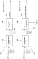
- FIG. 1a shows a block diagram of a conventional analogue envelope detector demodulator arrangement 100.
- An incoming modulated signal 102 is fed into an analogue envelope detector 104.
- This envelope detector 104 could take the form of a simple rectifier.
- the envelope detector 104 produces as an output an envelope signal 106.
- This envelope signal 106 has a shape that closely follows the envelope of the input modulated signal 102.
- the resulting envelope signal 106 is then fed into a comparator 108 that compares the envelope signal 106 to a threshold in order to produce a demodulated signal 110.
- FIG. 1b shows a block diagram of a conventional phase-locked loop demodulation arrangement 200.
- An incoming modulated signal 202 is fed into a sine-to-square convertor 204 which produces as an output a square wave 206.
- This square wave 206 has a fixed phase relationship with the incoming modulated signal 202 as will be detailed further with reference to Figure 2 .
- a phase-locked loop with lock-detect 208 takes the square wave 206 as a first input and a matched frequency local oscillator 207 as a second input. During a modulation symbol, there is no longer a phase relationship between the square wave 206 and the oscillator 207 and so the phase-locked loop loses lock.
- the signal that signifies when the phase-locked loop does and does not have lock provides as an output a demodulated signal 210.
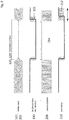
- FIG 2 shows timing diagrams for the conventional analogue envelope detector demodulator arrangement 100 of Figure 1a and the phase detector demodulator arrangement 200 of Figure 1b , showing the nature of the signals associated therewith as a function of time.
- the modulated signal 102,202 is composed of a carrier signal (in this example the carrier signal is a sinusoidal waveform) that has been modulated using amplitude modulation (AM) techniques, such that the envelope of the resulting modulated signal 102,202 conveys symbols, in this case of two distinct signal levels.
- the length of the symbol 120,220 is the duration for which the signal level is below a given threshold.
- the modulated signal 102 is processed by the envelope detector 104 and a demodulated signal 110 is obtained.
- the envelope of the demodulated signal 110 follows the envelope of the modulated signal 102, and has undergone a threshold operation to define the symbol edges.
- the degree of uncertainty 122 in the end of the modulation symbol which leads to the length of the symbol present in the demodulated signal 110 being different to the length of the symbol 120 as originally present in the modulated signal 102.
- the modulated signal 202 is processed by the sine-to-square converter 204 which produces a converted square wave signal 206.
- the converted square wave signal 206 has the same frequency as the modulated signal 202.
- the converted square wave signal 206 remains constant for a square wave symbol duration 214.
- the converted square wave signal 206 latches high or low during a modulation symbol 220 but which one it will be is not predictable and may change each time.
- the converted square wave signal 206 is then input to a phase-locked loop with lock detector 208.
- the phase-locked loop with lock detector 208 has a local free running oscillator 207 that runs at the carrier frequency and compares the local oscillator signal 207 to the converted square wave signal 206 and determines a phase relationship between the two signals and produces an output signal 210.
- the output signal 210 is high when the phase-locked loop has established lock (i.e. there is a fixed phase relationship between the local oscillator signal and the converted square wave signal 206). In contrast, the output signal 210 is low when no lock can be established, which occurs when a modulation symbol 220 is present, causing the converted square wave signal 206 to remain constant for a square wave symbol duration 214, removing the phase relationship between the converted square wave signal 206 and the local oscillator signal.
- the output signal 210 follows the general shape of the modulating signal that formed the modulated signal 202, thus providing a demodulated signal. However, the demodulated output signal 210 has a degree of uncertainty 212 regarding the position of the end of the modulation symbol due to the variable time taken to re-establish lock.
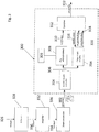
- FIG. 3 shows a block diagram of an exemplary embodiment of the present invention e.g. for use in a two-way radio communication system.
- An antenna 328 receives an incoming signal 326, and provides a received signal 330 to an amplifier 332.
- the received signal 330 is amplified by the amplifier 332 to provide sufficient amplitude for use by the demodulator 300.
- An amplified signal 334 is then processed by a down converter 336 to produce a modulated signal input 302 suitable for demodulation.
- the down converter and/or amplifier may not be needed.
- the incoming modulated signal 302 is directed into a sine-to-square converter 304 which produces a converted square wave signal 306.
- the converted square wave signal 306 is then input to a phase-locked loop with lock detector 308.
- the phase-locked loop with lock detector 308 has a local free running oscillator 309 that runs at the carrier frequency and compares this local oscillator signal to the converted square wave signal 306 and determines a phase relationship between the two signals and produces a lock detection signal 310.
- the converted square wave signal 306 is also input to an edge detector 314.
- the edge detector 314 comprises two latches, the first of which provides a positive edge signal 318 that latches to a logic high value when the converted square wave signal 306 is above a predetermined threshold value, the second of which provides a negative edge signal 320 that latches to a logic high value when the converted square wave signal 306 is below another predetermined threshold value.
- the lock detection signal 310 is input to a combiner 312 that monitors for the presence of a modulation symbol and provides a latch reset signal 316 to the edge detector 314.
- This combiner 312 also takes the positive 318 and negative 320 edge signals and combines these inputs with the lock detection signal 310 to produce a demodulated output signal 322, as will be explained further with reference to Figure 4 below.
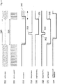
- Figure 4 is a timing diagram of the exemplary embodiment of the present invention shown in Figure 3 and shows the nature of the signals associated with the various components of the invention as a function of time.
- the modulated signal 302 is composed of a carrier signal (in this example the carrier signal is a sinusoidal waveform) that has been modulated using amplitude modulation (AM) techniques, such that the envelope of the resulting modulated signal 302 conveys symbols, in this case of two distinct signal levels.
- the length of the symbol 340 is the duration for which the signal level is below a given threshold.
- the modulated signal 302 is processed by the sine-to-square converter 304 which produces a converted square wave signal 306.
- the converted square wave signal 306 has the same frequency as the modulated signal 302. However, during a modulation symbol 340, the converted square wave signal 306 remains constant for a square wave symbol duration 314. Due to hysteresis present in the sine-to-square converter 304, the converted square wave signal 306 latches high or low during a modulation symbol 340 but it is not predictable which it will be and may change each time.
- the lock detection signal 310 of the phase-locked loop with lock detector 308 is high when the phase-locked loop has established lock (i.e. there is a fixed phase relationship between the local oscillator signal and the converted square wave signal 306). In contrast, the lock detection signal 310 is low when no lock can be established, which occurs when a modulation symbol 340 is present, causing the converted square wave signal 306 to remain constant for a square wave symbol duration 314, removing the phase relationship between the converted square wave signal 306 and the local oscillator signal.
- the output signal 310 follows the general shape of the modulating signal that formed the modulated signal 302, thus providing a demodulated signal. However, the lock detection signal 310 has a degree of uncertainty 346 regarding the position of the end of the modulation symbol.
- a combiner 312 monitors the lock detection signal 310. Once the lock detection signal 310 has been low for a predetermined length of time (indicating that a modulation symbol 340 is present), the combiner 312 provides a latch reset signal 316 to the edge detector 314 which resets both latches to a logic low value 352. As the latches trigger with respect to a threshold, as soon as the latch reset signal 316 is removed, one of the two latches will immediately trigger, but it is not known in advance which one will trigger due to the hysteresis in the sine-to-square converter 304 as explained above. The combiner 312 detects the triggering of the first latch and then monitors for the triggering of the second latch, as this will signify the end of the modulation symbol 340.
- the positive edge signal 318 immediately triggers to a logic high value 354, signifying that the combiner 312 must monitor for the negative edge signal 320 to trigger to a logic high value at a later time 356.
- the lock detection signal 310 is then combined with the more accurate detected negative edge signal 320 to produce the demodulated output signal 322 that has a narrower window of uncertainty 348 when compared to the uncertainty 346 associated with the lock detection signal 310 as used in the conventional phase-locked loop demodulation arrangement of Figure 1b .
Landscapes
- Engineering & Computer Science (AREA)
- Computer Networks & Wireless Communication (AREA)
- Signal Processing (AREA)
- Power Engineering (AREA)
- Digital Transmission Methods That Use Modulated Carrier Waves (AREA)
- Circuits Of Receivers In General (AREA)
Description
- This invention relates to demodulating amplitude modulated (AM) signals, particularly radio signals e.g. as used in short range data communication.
- When demodulating signals it is sometimes necessary to determine accurately the edges of modulation symbols. For example, a wireless communication system may be configured such that a transmitter transmits AM signals comprising a periodic carrier signal modulated by modulation symbols to a receiver that must demodulate the AM signals in order to recover the information or data contained within the signal. If, for example, the signal conveys digital data comprising a repeating pattern carrier wherein the amplitude varies between two pre-determined levels, the accurate timing of the end of each modulation symbol can be critical to the operation of the system, particularly regarding starting timers that are used to set a starting point for a response at an exact point in time.
- When demodulating AM modulation symbols from a modulated signal, it is known to use an envelope detector to extract a signal envelope that conveys the general shape of a modulating signal which, in general, will follow the modulating symbols that generated the modulated signal. Such an envelope detector often comprises a simple rectifier where the output signal of the rectifier is filtered using an analogue filter and then fed to a comparator to provide a demodulated signal.
- The analogue filter used in such a solution typically suffers from process variation (differences between devices due to manufacturing processes) which may lead to inaccurate detection of the actual envelope and uncertainties in the timing of modulation symbol edges.
- It is also known to use a phase locked loop (PLL) for demodulation in the case where only AM techniques have been used in the modulation of the signal. In such a system, both the modulated signal and a local oscillator signal are fed to a phase detector. When the input signal is modulated by suppressing the carrier, the phase detector will not sense any signal on the reference input and the PLL will lose phase lock. By using a simple lock detector circuit, known per se to a person skilled in the art, demodulation can be achieved.
US 4,947,407 describes a detection circuit featuring a digital phase locked loop along with decision logic for demodulating a carrier signal modulated with amplitude shift keying. - A disadvantage of using a PLL is that the time that is required to detect phase lock depends upon the oscillator free-running frequency, which itself is typically dependent upon analogue process variation of the analogue components.
- The present invention sets out to provide an alternative approach.
- From a first aspect, the invention provides a method of demodulating an amplitude modulated radio signal according to
claim 1. - From a second aspect, the invention provides a receiver arranged to demodulate an amplitude modulated radio signal according to claim 9.
- Thus it will be seen by those skilled in the art that, in accordance with the invention, a receiver directs a modulated radio signal to both a phase detector in order to obtain the envelope of the modulated signal, and an edge detector which can determine an edge in the modulated signal. The outputs from both detectors can be used to determine the end of a modulation symbol and thus provide a demodulated signal output.
- Using both a phase detector and an edge detector provides the ability to obtain a demodulated signal that has a reduced uncertainty with regard to the end of modulation symbols when compared to conventional systems without the edge detector.
- There are a number of phase detector circuits known per se in the art. In some sets of embodiments, the phase detector comprises a phase locked loop and a lock detector.
- In order to determine whether a modulation symbol is present, it is advantageous to convert the input signal, which is conventionally sinusoidal, to a square wave before providing it as an input to the phase detector. In some sets of embodiments, the modulated signal is fed to a sine-to-square converter.
- The square wave output referred to above can be used to determine when modulation symbols are present on the modulated signal. In some further sets of embodiments, the output of the sine-to-square converter comprises a square wave when no modulation symbol is present and a constant value when a modulation symbol is present.
- It is typically not always known in advance whether the square wave output will comprise a logic high or a logic low value when a modulation signal is present due to the nature of sine-to-square converter circuits. It is common for sine-to-square converters (such as those that utilise Schmitt triggers) to have hysteresis, such that it is not known what value the output will take when the input is below a threshold voltage required to overcome said hysteresis.
- The end of modulation symbols present on the modulated signal may be determined by monitoring for a change in the value of the edge detector input from a first constant value to a second value. In some sets of embodiments, the edge detector comprises a first output that latches to a first level when the input to the edge detector is above a first threshold value, and a second output that latches to a second level when the input to the edge detector is below a second threshold value. The first and second thresholds may be the same but typically they are different.
- The edge detector could produce an output continuously. In a set of embodiments however it instead monitors for the end of a modulation symbol only once it is known that such a modulation symbol is currently present on the modulated signal. In some sets of embodiments therefore, a combiner is provided which is arranged to reset the edge detector after the phase detector has detected a modulation symbol.
- When it is determined that a modulation symbol is present on the modulated signal and the edge detector has been reset, it is then advantageous to monitor for the end of the modulation symbol. Due to the above-mentioned hysteresis effect present on the sine-to-square converter, it is typically not known in advance whether the end of the modulation symbol will be signified by a low-to-high transition or a high-to-low transition, but it is possible to determine the current level of the signal and monitor for a change to the corresponding opposite level. A combiner is arranged to detect the first output of the edge detector latching to the first output value after resetting the edge detector and monitors for the second output of the edge detector latching to the second output value.
- After some time, the modulation symbol will end and the output from the sine-to-square converter will no longer remain constant. In a further set of embodiments, the second output of the edge detector latching to a second output value may be used to indicate the end of the modulation symbol.
- In general there is a possibility that errors can occur in any given demodulation scheme and it is advantageous in some circumstances to reduce these errors by validating a detected end of a modulation symbol to ensure that it is genuine. In some sets of embodiments, an edge detected by the edge detector is validated by checking that the edge is followed by the phase detector output going high.
- In some sets of embodiments, the demodulator is implemented in a battery powered integrated circuit.
- A person skilled in the art would understand that the present invention has applications in a wide range of communication technologies. In some sets of embodiments, the demodulation is provided for use in near field communication (NFC) systems.
- A person skilled in the art would also understand that the carrier referred to with regard to the present invention is not limited to a sinusoidal waveform and could comprise other forms including, but not limited to, square waves, saw-tooth waves triangular waves or other periodic waveforms.
- An embodiment of the present invention will now be described, by way of example only, with reference to the accompanying drawings, in which:
-
Figure 1a is a block diagram of a conventional analogue envelope detector; -
Figure 1b is a block diagram of a conventional phase-locked loop demodulator; -
Figure 2 is a timing diagram of a conventional simple analogue envelope detector and a conventional phase-locked loop demodulator; -
Figure 3 is a block diagram of an exemplary embodiment of the present invention; and -
Figure 4 is a timing diagram of an exemplary embodiment of the present invention. -
Figure 1a shows a block diagram of a conventional analogue envelopedetector demodulator arrangement 100. An incoming modulatedsignal 102 is fed into ananalogue envelope detector 104. Thisenvelope detector 104 could take the form of a simple rectifier. Theenvelope detector 104 produces as an output anenvelope signal 106. Thisenvelope signal 106 has a shape that closely follows the envelope of the input modulatedsignal 102. The resultingenvelope signal 106 is then fed into acomparator 108 that compares theenvelope signal 106 to a threshold in order to produce a demodulatedsignal 110. -
Figure 1b shows a block diagram of a conventional phase-lockedloop demodulation arrangement 200. An incoming modulatedsignal 202 is fed into a sine-to-square convertor 204 which produces as an output asquare wave 206. Thissquare wave 206 has a fixed phase relationship with the incoming modulatedsignal 202 as will be detailed further with reference toFigure 2 . A phase-locked loop with lock-detect 208 takes thesquare wave 206 as a first input and a matched frequencylocal oscillator 207 as a second input. During a modulation symbol, there is no longer a phase relationship between thesquare wave 206 and theoscillator 207 and so the phase-locked loop loses lock. The signal that signifies when the phase-locked loop does and does not have lock provides as an output a demodulatedsignal 210. -
Figure 2 shows timing diagrams for the conventional analogue envelopedetector demodulator arrangement 100 ofFigure 1a and the phasedetector demodulator arrangement 200 ofFigure 1b , showing the nature of the signals associated therewith as a function of time. - The modulated signal 102,202 is composed of a carrier signal (in this example the carrier signal is a sinusoidal waveform) that has been modulated using amplitude modulation (AM) techniques, such that the envelope of the resulting modulated signal 102,202 conveys symbols, in this case of two distinct signal levels. The length of the symbol 120,220 is the duration for which the signal level is below a given threshold.
- When using the analogue envelope
detector demodulator arrangement 100, the modulatedsignal 102 is processed by theenvelope detector 104 and ademodulated signal 110 is obtained. Here it can be seen that the envelope of thedemodulated signal 110 follows the envelope of the modulatedsignal 102, and has undergone a threshold operation to define the symbol edges. However, as can be seen in the Figure, due to inevitable process variation in the components of the edge detector, there is a degree ofuncertainty 122 in the end of the modulation symbol, which leads to the length of the symbol present in thedemodulated signal 110 being different to the length of the symbol 120 as originally present in the modulatedsignal 102. - When using the phase-locked
loop demodulation arrangement 200, the modulatedsignal 202 is processed by the sine-to-square converter 204 which produces a convertedsquare wave signal 206. When no modulation symbol 220 is present, the convertedsquare wave signal 206 has the same frequency as the modulatedsignal 202. However, during a modulation symbol 220, the convertedsquare wave signal 206 remains constant for a squarewave symbol duration 214. The convertedsquare wave signal 206 latches high or low during a modulation symbol 220 but which one it will be is not predictable and may change each time. - In this conventional phase-locked loop demodulation arrangement 200 (
Figure 1b ), the convertedsquare wave signal 206 is then input to a phase-locked loop withlock detector 208. The phase-locked loop withlock detector 208 has a localfree running oscillator 207 that runs at the carrier frequency and compares thelocal oscillator signal 207 to the convertedsquare wave signal 206 and determines a phase relationship between the two signals and produces anoutput signal 210. - The
output signal 210 is high when the phase-locked loop has established lock (i.e. there is a fixed phase relationship between the local oscillator signal and the converted square wave signal 206). In contrast, theoutput signal 210 is low when no lock can be established, which occurs when a modulation symbol 220 is present, causing the convertedsquare wave signal 206 to remain constant for a squarewave symbol duration 214, removing the phase relationship between the convertedsquare wave signal 206 and the local oscillator signal. Theoutput signal 210 follows the general shape of the modulating signal that formed the modulatedsignal 202, thus providing a demodulated signal. However, thedemodulated output signal 210 has a degree ofuncertainty 212 regarding the position of the end of the modulation symbol due to the variable time taken to re-establish lock. -
Figure 3 shows a block diagram of an exemplary embodiment of the present invention e.g. for use in a two-way radio communication system. Anantenna 328 receives anincoming signal 326, and provides a receivedsignal 330 to an amplifier 332. The receivedsignal 330 is amplified by the amplifier 332 to provide sufficient amplitude for use by thedemodulator 300. An amplifiedsignal 334 is then processed by adown converter 336 to produce a modulatedsignal input 302 suitable for demodulation. In other embodiments e.g. in a near-field communication (NFC) implementation the down converter and/or amplifier may not be needed. The incoming modulatedsignal 302 is directed into a sine-to-square converter 304 which produces a convertedsquare wave signal 306. - The converted
square wave signal 306 is then input to a phase-locked loop withlock detector 308. The phase-locked loop withlock detector 308 has a localfree running oscillator 309 that runs at the carrier frequency and compares this local oscillator signal to the convertedsquare wave signal 306 and determines a phase relationship between the two signals and produces alock detection signal 310. - The converted
square wave signal 306 is also input to anedge detector 314. Theedge detector 314 comprises two latches, the first of which provides apositive edge signal 318 that latches to a logic high value when the convertedsquare wave signal 306 is above a predetermined threshold value, the second of which provides anegative edge signal 320 that latches to a logic high value when the convertedsquare wave signal 306 is below another predetermined threshold value. - The
lock detection signal 310 is input to acombiner 312 that monitors for the presence of a modulation symbol and provides a latch reset signal 316 to theedge detector 314. Thiscombiner 312 also takes the positive 318 and negative 320 edge signals and combines these inputs with thelock detection signal 310 to produce ademodulated output signal 322, as will be explained further with reference toFigure 4 below. -
Figure 4 is a timing diagram of the exemplary embodiment of the present invention shown inFigure 3 and shows the nature of the signals associated with the various components of the invention as a function of time. - The modulated
signal 302 is composed of a carrier signal (in this example the carrier signal is a sinusoidal waveform) that has been modulated using amplitude modulation (AM) techniques, such that the envelope of the resulting modulatedsignal 302 conveys symbols, in this case of two distinct signal levels. The length of thesymbol 340 is the duration for which the signal level is below a given threshold. - When using the phase-locked
loop demodulation arrangement 300, the modulatedsignal 302 is processed by the sine-to-square converter 304 which produces a convertedsquare wave signal 306. When nomodulation symbol 340 is present, the convertedsquare wave signal 306 has the same frequency as the modulatedsignal 302. However, during amodulation symbol 340, the convertedsquare wave signal 306 remains constant for a squarewave symbol duration 314. Due to hysteresis present in the sine-to-square converter 304, the convertedsquare wave signal 306 latches high or low during amodulation symbol 340 but it is not predictable which it will be and may change each time. - The
lock detection signal 310 of the phase-locked loop withlock detector 308 is high when the phase-locked loop has established lock (i.e. there is a fixed phase relationship between the local oscillator signal and the converted square wave signal 306). In contrast, thelock detection signal 310 is low when no lock can be established, which occurs when amodulation symbol 340 is present, causing the convertedsquare wave signal 306 to remain constant for a squarewave symbol duration 314, removing the phase relationship between the convertedsquare wave signal 306 and the local oscillator signal. Theoutput signal 310 follows the general shape of the modulating signal that formed the modulatedsignal 302, thus providing a demodulated signal. However, thelock detection signal 310 has a degree ofuncertainty 346 regarding the position of the end of the modulation symbol. - A
combiner 312 monitors thelock detection signal 310. Once thelock detection signal 310 has been low for a predetermined length of time (indicating that amodulation symbol 340 is present), thecombiner 312 provides a latch reset signal 316 to theedge detector 314 which resets both latches to a logiclow value 352. As the latches trigger with respect to a threshold, as soon as the latch resetsignal 316 is removed, one of the two latches will immediately trigger, but it is not known in advance which one will trigger due to the hysteresis in the sine-to-square converter 304 as explained above. Thecombiner 312 detects the triggering of the first latch and then monitors for the triggering of the second latch, as this will signify the end of themodulation symbol 340. - As at this time the converted
square wave signal 306 is high, thepositive edge signal 318 immediately triggers to a logichigh value 354, signifying that thecombiner 312 must monitor for thenegative edge signal 320 to trigger to a logic high value at alater time 356. - The
lock detection signal 310 is then combined with the more accurate detectednegative edge signal 320 to produce thedemodulated output signal 322 that has a narrower window ofuncertainty 348 when compared to theuncertainty 346 associated with thelock detection signal 310 as used in the conventional phase-locked loop demodulation arrangement ofFigure 1b . - It is then possible to validate the detected edge by checking that the
lock detection signal 310 returns to a logic high value after the negative edge signal triggers to a logichigh value 356. This produces a demodulated signal withvalidation 324 that has a slight time delay when compared to the demodulated signal withoutvalidation 322. - Thus it will be seen that a method for demodulating a modulated signal wherein symbol edges can be determined with less analogue process variation than in conventional methods has been described.
- The invention is solely limited by the appended claims.
Claims (15)
- A method of demodulating an amplitude modulated radio signal (302) comprising directing said modulated signal (302) to both a phase detector (308) and an edge detector (314), and using the respective output signals (310, 318, 320) of the phase detector (308) and edge detector (318) to determine an end of a modulation symbol (340) in said signal (302);
wherein the method further comprises:
detecting a first output (318) of the edge detector (314) latching to a first output value after resetting the edge detector (314) and monitoring for a second output (320) of the edge detector (314) latching to a second output value. - A method as claimed in claim 1 wherein the phase detector (308) comprises a phase locked loop and a lock detector.
- A method as claimed in claim 1 or 2 comprising feeding the modulated signal (302) to a sine-to-square converter (304), wherein preferably an output of the sine-to-square converter (304) comprises a square wave when no modulation symbol is present and a constant value when a modulation symbol (340) is present.
- A method as claimed in any preceding claim wherein the edge detector (314) comprises a first output (318) that latches to a first level when the input to the edge detector (314) is above a first threshold value, and a second output (320) that latches to a second level when the input to the edge detector (314) is below a second threshold value.
- A method as claimed in any preceding claim comprising resetting the edge detector (314) after the phase detector (308) has detected a modulation symbol (340).
- A method as claimed in any preceding claim comprising using the second output (320) of the edge detector (318) latching to a second output value to indicate the end of the modulation symbol (340).
- A method as claimed in any preceding claim comprising validating an edge detected by the edge detector (318) by checking that the edge is followed by the phase detector output (310) going high.
- A method as claimed in any preceding claim wherein the demodulator (300) is implemented in a battery powered integrated circuit.
- A receiver arranged to demodulate an amplitude modulated radio signal (302) comprising a phase detector (308) and an edge detector (314) that are both arranged to receive the modulated signal (302), the receiver being arranged to use the respective output signals (310, 318, 320) of the phase detector (308) and edge detector (314) to determine an end of a modulation symbol (340) in said modulated signal (302); wherein the receiver comprises a combiner (312) arranged to detect a first output (318) of the edge detector (314) latching to a first output value after resetting the edge detector (314), and to monitor for a second output (320) of the edge detector (314) latching to a second output value.
- A receiver as claimed in claim 9 wherein the phase detector (308) comprises a phase locked loop and a lock detector.
- A receiver as claimed in claim 9 or 10 wherein the modulated signal (302) is fed to a sine-to-square converter (304), wherein preferably an output of the sine-to-square converter (304) comprises a square wave when no modulation symbol is present and a constant value when a modulation symbol (304) is present.
- A receiver as claimed in any of claims 9 to 11 comprising a combiner (312) arranged to reset the edge detector (314) after the phase detector (308) has detected a modulation symbol (340).
- A receiver as claimed in any of claims 9 to 12, wherein the second output of the edge detector (314) latching to a second output value is used to indicate the end of the modulation symbol (340).
- A receiver as claimed in any of claims 9 to 13 wherein an edge detected by the edge detector (314) is validated by checking that the edge is followed by the phase detector (308) output going high.
- A receiver as claimed in claims 9 to 14 wherein the demodulator (300) is implemented in a battery powered integrated circuit.
Applications Claiming Priority (2)
| Application Number | Priority Date | Filing Date | Title |
|---|---|---|---|
| GB1420711.2A GB2532491A (en) | 2014-11-21 | 2014-11-21 | AM demodulation |
| PCT/GB2015/053543 WO2016079534A1 (en) | 2014-11-21 | 2015-11-20 | Am demodulation with phase and symbol edge detection |
Publications (2)
| Publication Number | Publication Date |
|---|---|
| EP3222016A1 EP3222016A1 (en) | 2017-09-27 |
| EP3222016B1 true EP3222016B1 (en) | 2020-10-07 |
Family
ID=52292325
Family Applications (1)
| Application Number | Title | Priority Date | Filing Date |
|---|---|---|---|
| EP15800923.3A Active EP3222016B1 (en) | 2014-11-21 | 2015-11-20 | Am demodulation with phase and symbol edge detection |
Country Status (8)
| Country | Link |
|---|---|
| US (1) | US10153927B2 (en) |
| EP (1) | EP3222016B1 (en) |
| JP (1) | JP6769961B2 (en) |
| KR (1) | KR102415697B1 (en) |
| CN (1) | CN107005510B (en) |
| GB (1) | GB2532491A (en) |
| TW (1) | TWI675561B (en) |
| WO (1) | WO2016079534A1 (en) |
Families Citing this family (3)
| Publication number | Priority date | Publication date | Assignee | Title |
|---|---|---|---|---|
| US10447350B2 (en) | 2017-01-11 | 2019-10-15 | Mediatek Singapore Pte. Ltd. | High-speed circuits for active load modulation and related methods |
| US10491437B2 (en) | 2017-01-11 | 2019-11-26 | Mediatek Singapore Pte. Ltd. | Circuits for amplitude demodulation and related methods |
| US10374848B2 (en) * | 2017-01-11 | 2019-08-06 | Mediatek Singapore Pte. Ltd. | Amplitude demodulators and related methods |
Family Cites Families (18)
| Publication number | Priority date | Publication date | Assignee | Title |
|---|---|---|---|---|
| KR900002535A (en) * | 1988-07-11 | 1990-02-28 | 지대훈 | Amplitude Modulation Using A-D Converter |
| US4947407A (en) * | 1989-08-08 | 1990-08-07 | Siemens-Pacesetter, Inc. | Sample-and-hold digital phase-locked loop for ask signals |
| DE19858099C2 (en) * | 1998-12-16 | 2000-12-07 | Texas Instruments Deutschland | Demodulator circuit |
| KR100655784B1 (en) * | 2001-02-08 | 2006-12-12 | 넥스원퓨처 주식회사 | Demodulator with digital intermediate frequency down converter |
| JP4216714B2 (en) * | 2001-07-20 | 2009-01-28 | エヌエックスピー ビー ヴィ | Signal edge recognition method and means |
| KR100434501B1 (en) * | 2002-04-25 | 2004-06-05 | 삼성전자주식회사 | Duty correction based frequency multiplier |
| US7099400B2 (en) * | 2003-01-22 | 2006-08-29 | Agere Systems Inc. | Multi-level pulse amplitude modulation receiver |
| US7477716B2 (en) * | 2003-06-25 | 2009-01-13 | Mosaid Technologies, Inc. | Start up circuit for delay locked loop |
| KR100656339B1 (en) * | 2003-12-26 | 2006-12-11 | 한국전자통신연구원 | Pulse signal generator for ultra-wide band radio transceiving and radio transceiver having the same |
| WO2006047540A2 (en) * | 2004-10-25 | 2006-05-04 | Avaak Inc. | Simplified radio frequency receiver |
| US9794096B2 (en) * | 2005-06-27 | 2017-10-17 | John W. Bogdan | Direct synchronization of synthesized clock |
| US7907005B2 (en) * | 2007-01-31 | 2011-03-15 | Nxp B.V. | Demodulation circuit for ASK coded or amplitude modulated signals as wells as NFC and RFID devices comprising the same |
| US8401092B1 (en) * | 2010-07-30 | 2013-03-19 | Broadlogic Network Technologies Inc. | Multi-reference clock synchronization techniques |
| JP5653791B2 (en) * | 2011-02-18 | 2015-01-14 | ラピスセミコンダクタ株式会社 | FSK demodulation circuit |
| TWI451700B (en) * | 2011-12-05 | 2014-09-01 | Global Unichip Corp | Clock and data recovery circuit |
| CN103905370B (en) * | 2012-12-27 | 2017-05-24 | 展讯通信(上海)有限公司 | Soft demodulation method and device for quadrature amplitude modulation (QAM) signal and mobile terminal |
| CN103346988B (en) * | 2013-06-13 | 2016-03-23 | 电子科技大学 | A kind of FSK digital demodulator |
| US9553717B2 (en) * | 2014-03-18 | 2017-01-24 | Analog Devices Global | Systems and methods for clock and data recovery |
-
2014
- 2014-11-21 GB GB1420711.2A patent/GB2532491A/en not_active Withdrawn
-
2015
- 2015-11-13 TW TW104137495A patent/TWI675561B/en active
- 2015-11-20 KR KR1020177016913A patent/KR102415697B1/en active Active
- 2015-11-20 EP EP15800923.3A patent/EP3222016B1/en active Active
- 2015-11-20 US US15/528,433 patent/US10153927B2/en active Active
- 2015-11-20 CN CN201580063321.9A patent/CN107005510B/en active Active
- 2015-11-20 WO PCT/GB2015/053543 patent/WO2016079534A1/en not_active Ceased
- 2015-11-20 JP JP2017527632A patent/JP6769961B2/en active Active
Non-Patent Citations (1)
| Title |
|---|
| None * |
Also Published As
| Publication number | Publication date |
|---|---|
| JP2018502487A (en) | 2018-01-25 |
| WO2016079534A1 (en) | 2016-05-26 |
| US10153927B2 (en) | 2018-12-11 |
| GB201420711D0 (en) | 2015-01-07 |
| US20180183637A1 (en) | 2018-06-28 |
| KR102415697B1 (en) | 2022-06-30 |
| KR20170088913A (en) | 2017-08-02 |
| GB2532491A (en) | 2016-05-25 |
| TW201620261A (en) | 2016-06-01 |
| TWI675561B (en) | 2019-10-21 |
| CN107005510A (en) | 2017-08-01 |
| JP6769961B2 (en) | 2020-10-14 |
| EP3222016A1 (en) | 2017-09-27 |
| CN107005510B (en) | 2020-09-25 |
Similar Documents
| Publication | Publication Date | Title |
|---|---|---|
| US10187100B2 (en) | Apparatus and method for direct radio frequency (RF) sampling in near field communication (NFC) devices | |
| US7949075B2 (en) | Data slicer circuit, demodulation stage, receiving system and method for demodulating shift key coded signals | |
| CN102594752A (en) | FSK radio signal receiver and method for operating said receiver | |
| US9705544B2 (en) | Wireless receiver and method | |
| CN108306838B (en) | Demodulator and method for demodulating amplitude modulated input signal | |
| US8718196B2 (en) | Symbol error detection for Bluetooth basic data rate packets | |
| US20180263001A1 (en) | Method of operating a receiver to process a preamble of a data packet, and to a receiver operating in accordance with the method | |
| US10153927B2 (en) | AM demodulation with phase and symbol edge detection | |
| US8638884B2 (en) | Data processing unit and signal receiver including the data processing unit | |
| KR102484067B1 (en) | Method and apparatus for receiving a phase or frequency signal modulated by a sequence of two state symbols | |
| KR101060303B1 (en) | ON and FSS dual mode demodulation method and apparatus | |
| JP5326759B2 (en) | FSK receiving apparatus, FSK receiving method, and program | |
| JP2011087212A (en) | Demodulation device and method, and electronic equipment | |
| CN108183876B (en) | FSK signal demodulation and pulse recovery system and method | |
| JP2006261826A (en) | Receiving apparatus and receiving method | |
| CN116155668A (en) | Method, system and storage medium for anti-frequency offset carrier recovery | |
| JP2008028666A (en) | Wireless communication device | |
| HK1170867B (en) | Data processing unit and signal receiver including the data processing unit |
Legal Events
| Date | Code | Title | Description |
|---|---|---|---|
| STAA | Information on the status of an ep patent application or granted ep patent |
Free format text: STATUS: THE INTERNATIONAL PUBLICATION HAS BEEN MADE |
|
| PUAI | Public reference made under article 153(3) epc to a published international application that has entered the european phase |
Free format text: ORIGINAL CODE: 0009012 |
|
| STAA | Information on the status of an ep patent application or granted ep patent |
Free format text: STATUS: REQUEST FOR EXAMINATION WAS MADE |
|
| 17P | Request for examination filed |
Effective date: 20170620 |
|
| AK | Designated contracting states |
Kind code of ref document: A1 Designated state(s): AL AT BE BG CH CY CZ DE DK EE ES FI FR GB GR HR HU IE IS IT LI LT LU LV MC MK MT NL NO PL PT RO RS SE SI SK SM TR |
|
| AX | Request for extension of the european patent |
Extension state: BA ME |
|
| DAV | Request for validation of the european patent (deleted) | ||
| DAX | Request for extension of the european patent (deleted) | ||
| GRAP | Despatch of communication of intention to grant a patent |
Free format text: ORIGINAL CODE: EPIDOSNIGR1 |
|
| STAA | Information on the status of an ep patent application or granted ep patent |
Free format text: STATUS: GRANT OF PATENT IS INTENDED |
|
| INTG | Intention to grant announced |
Effective date: 20191023 |
|
| GRAJ | Information related to disapproval of communication of intention to grant by the applicant or resumption of examination proceedings by the epo deleted |
Free format text: ORIGINAL CODE: EPIDOSDIGR1 |
|
| STAA | Information on the status of an ep patent application or granted ep patent |
Free format text: STATUS: REQUEST FOR EXAMINATION WAS MADE |
|
| INTC | Intention to grant announced (deleted) | ||
| GRAP | Despatch of communication of intention to grant a patent |
Free format text: ORIGINAL CODE: EPIDOSNIGR1 |
|
| STAA | Information on the status of an ep patent application or granted ep patent |
Free format text: STATUS: GRANT OF PATENT IS INTENDED |
|
| INTG | Intention to grant announced |
Effective date: 20200421 |
|
| GRAS | Grant fee paid |
Free format text: ORIGINAL CODE: EPIDOSNIGR3 |
|
| GRAA | (expected) grant |
Free format text: ORIGINAL CODE: 0009210 |
|
| STAA | Information on the status of an ep patent application or granted ep patent |
Free format text: STATUS: THE PATENT HAS BEEN GRANTED |
|
| AK | Designated contracting states |
Kind code of ref document: B1 Designated state(s): AL AT BE BG CH CY CZ DE DK EE ES FI FR GB GR HR HU IE IS IT LI LT LU LV MC MK MT NL NO PL PT RO RS SE SI SK SM TR |
|
| REG | Reference to a national code |
Ref country code: GB Ref legal event code: FG4D |
|
| REG | Reference to a national code |
Ref country code: CH Ref legal event code: EP Ref country code: AT Ref legal event code: REF Ref document number: 1322374 Country of ref document: AT Kind code of ref document: T Effective date: 20201015 |
|
| REG | Reference to a national code |
Ref country code: IE Ref legal event code: FG4D |
|
| REG | Reference to a national code |
Ref country code: DE Ref legal event code: R096 Ref document number: 602015060214 Country of ref document: DE |
|
| REG | Reference to a national code |
Ref country code: NL Ref legal event code: MP Effective date: 20201007 |
|
| REG | Reference to a national code |
Ref country code: AT Ref legal event code: MK05 Ref document number: 1322374 Country of ref document: AT Kind code of ref document: T Effective date: 20201007 |
|
| PG25 | Lapsed in a contracting state [announced via postgrant information from national office to epo] |
Ref country code: GR Free format text: LAPSE BECAUSE OF FAILURE TO SUBMIT A TRANSLATION OF THE DESCRIPTION OR TO PAY THE FEE WITHIN THE PRESCRIBED TIME-LIMIT Effective date: 20210108 Ref country code: FI Free format text: LAPSE BECAUSE OF FAILURE TO SUBMIT A TRANSLATION OF THE DESCRIPTION OR TO PAY THE FEE WITHIN THE PRESCRIBED TIME-LIMIT Effective date: 20201007 Ref country code: RS Free format text: LAPSE BECAUSE OF FAILURE TO SUBMIT A TRANSLATION OF THE DESCRIPTION OR TO PAY THE FEE WITHIN THE PRESCRIBED TIME-LIMIT Effective date: 20201007 Ref country code: PT Free format text: LAPSE BECAUSE OF FAILURE TO SUBMIT A TRANSLATION OF THE DESCRIPTION OR TO PAY THE FEE WITHIN THE PRESCRIBED TIME-LIMIT Effective date: 20210208 Ref country code: NL Free format text: LAPSE BECAUSE OF FAILURE TO SUBMIT A TRANSLATION OF THE DESCRIPTION OR TO PAY THE FEE WITHIN THE PRESCRIBED TIME-LIMIT Effective date: 20201007 Ref country code: NO Free format text: LAPSE BECAUSE OF FAILURE TO SUBMIT A TRANSLATION OF THE DESCRIPTION OR TO PAY THE FEE WITHIN THE PRESCRIBED TIME-LIMIT Effective date: 20210107 |
|
| REG | Reference to a national code |
Ref country code: LT Ref legal event code: MG4D |
|
| PG25 | Lapsed in a contracting state [announced via postgrant information from national office to epo] |
Ref country code: ES Free format text: LAPSE BECAUSE OF FAILURE TO SUBMIT A TRANSLATION OF THE DESCRIPTION OR TO PAY THE FEE WITHIN THE PRESCRIBED TIME-LIMIT Effective date: 20201007 Ref country code: AT Free format text: LAPSE BECAUSE OF FAILURE TO SUBMIT A TRANSLATION OF THE DESCRIPTION OR TO PAY THE FEE WITHIN THE PRESCRIBED TIME-LIMIT Effective date: 20201007 Ref country code: BG Free format text: LAPSE BECAUSE OF FAILURE TO SUBMIT A TRANSLATION OF THE DESCRIPTION OR TO PAY THE FEE WITHIN THE PRESCRIBED TIME-LIMIT Effective date: 20210107 Ref country code: PL Free format text: LAPSE BECAUSE OF FAILURE TO SUBMIT A TRANSLATION OF THE DESCRIPTION OR TO PAY THE FEE WITHIN THE PRESCRIBED TIME-LIMIT Effective date: 20201007 Ref country code: LV Free format text: LAPSE BECAUSE OF FAILURE TO SUBMIT A TRANSLATION OF THE DESCRIPTION OR TO PAY THE FEE WITHIN THE PRESCRIBED TIME-LIMIT Effective date: 20201007 Ref country code: IS Free format text: LAPSE BECAUSE OF FAILURE TO SUBMIT A TRANSLATION OF THE DESCRIPTION OR TO PAY THE FEE WITHIN THE PRESCRIBED TIME-LIMIT Effective date: 20210207 Ref country code: SE Free format text: LAPSE BECAUSE OF FAILURE TO SUBMIT A TRANSLATION OF THE DESCRIPTION OR TO PAY THE FEE WITHIN THE PRESCRIBED TIME-LIMIT Effective date: 20201007 |
|
| PG25 | Lapsed in a contracting state [announced via postgrant information from national office to epo] |
Ref country code: HR Free format text: LAPSE BECAUSE OF FAILURE TO SUBMIT A TRANSLATION OF THE DESCRIPTION OR TO PAY THE FEE WITHIN THE PRESCRIBED TIME-LIMIT Effective date: 20201007 |
|
| REG | Reference to a national code |
Ref country code: CH Ref legal event code: PL |
|
| REG | Reference to a national code |
Ref country code: DE Ref legal event code: R097 Ref document number: 602015060214 Country of ref document: DE |
|
| PG25 | Lapsed in a contracting state [announced via postgrant information from national office to epo] |
Ref country code: CZ Free format text: LAPSE BECAUSE OF FAILURE TO SUBMIT A TRANSLATION OF THE DESCRIPTION OR TO PAY THE FEE WITHIN THE PRESCRIBED TIME-LIMIT Effective date: 20201007 Ref country code: EE Free format text: LAPSE BECAUSE OF FAILURE TO SUBMIT A TRANSLATION OF THE DESCRIPTION OR TO PAY THE FEE WITHIN THE PRESCRIBED TIME-LIMIT Effective date: 20201007 Ref country code: SM Free format text: LAPSE BECAUSE OF FAILURE TO SUBMIT A TRANSLATION OF THE DESCRIPTION OR TO PAY THE FEE WITHIN THE PRESCRIBED TIME-LIMIT Effective date: 20201007 Ref country code: LU Free format text: LAPSE BECAUSE OF NON-PAYMENT OF DUE FEES Effective date: 20201120 Ref country code: MC Free format text: LAPSE BECAUSE OF FAILURE TO SUBMIT A TRANSLATION OF THE DESCRIPTION OR TO PAY THE FEE WITHIN THE PRESCRIBED TIME-LIMIT Effective date: 20201007 Ref country code: LT Free format text: LAPSE BECAUSE OF FAILURE TO SUBMIT A TRANSLATION OF THE DESCRIPTION OR TO PAY THE FEE WITHIN THE PRESCRIBED TIME-LIMIT Effective date: 20201007 Ref country code: RO Free format text: LAPSE BECAUSE OF FAILURE TO SUBMIT A TRANSLATION OF THE DESCRIPTION OR TO PAY THE FEE WITHIN THE PRESCRIBED TIME-LIMIT Effective date: 20201007 Ref country code: SK Free format text: LAPSE BECAUSE OF FAILURE TO SUBMIT A TRANSLATION OF THE DESCRIPTION OR TO PAY THE FEE WITHIN THE PRESCRIBED TIME-LIMIT Effective date: 20201007 |
|
| REG | Reference to a national code |
Ref country code: BE Ref legal event code: MM Effective date: 20201130 |
|
| PLBE | No opposition filed within time limit |
Free format text: ORIGINAL CODE: 0009261 |
|
| STAA | Information on the status of an ep patent application or granted ep patent |
Free format text: STATUS: NO OPPOSITION FILED WITHIN TIME LIMIT |
|
| PG25 | Lapsed in a contracting state [announced via postgrant information from national office to epo] |
Ref country code: CH Free format text: LAPSE BECAUSE OF NON-PAYMENT OF DUE FEES Effective date: 20201130 Ref country code: DK Free format text: LAPSE BECAUSE OF FAILURE TO SUBMIT A TRANSLATION OF THE DESCRIPTION OR TO PAY THE FEE WITHIN THE PRESCRIBED TIME-LIMIT Effective date: 20201007 Ref country code: LI Free format text: LAPSE BECAUSE OF NON-PAYMENT OF DUE FEES Effective date: 20201130 |
|
| 26N | No opposition filed |
Effective date: 20210708 |
|
| PG25 | Lapsed in a contracting state [announced via postgrant information from national office to epo] |
Ref country code: AL Free format text: LAPSE BECAUSE OF FAILURE TO SUBMIT A TRANSLATION OF THE DESCRIPTION OR TO PAY THE FEE WITHIN THE PRESCRIBED TIME-LIMIT Effective date: 20201007 Ref country code: IE Free format text: LAPSE BECAUSE OF NON-PAYMENT OF DUE FEES Effective date: 20201120 Ref country code: IT Free format text: LAPSE BECAUSE OF FAILURE TO SUBMIT A TRANSLATION OF THE DESCRIPTION OR TO PAY THE FEE WITHIN THE PRESCRIBED TIME-LIMIT Effective date: 20201007 |
|
| PG25 | Lapsed in a contracting state [announced via postgrant information from national office to epo] |
Ref country code: SI Free format text: LAPSE BECAUSE OF FAILURE TO SUBMIT A TRANSLATION OF THE DESCRIPTION OR TO PAY THE FEE WITHIN THE PRESCRIBED TIME-LIMIT Effective date: 20201007 |
|
| PG25 | Lapsed in a contracting state [announced via postgrant information from national office to epo] |
Ref country code: IS Free format text: LAPSE BECAUSE OF FAILURE TO SUBMIT A TRANSLATION OF THE DESCRIPTION OR TO PAY THE FEE WITHIN THE PRESCRIBED TIME-LIMIT Effective date: 20210207 Ref country code: TR Free format text: LAPSE BECAUSE OF FAILURE TO SUBMIT A TRANSLATION OF THE DESCRIPTION OR TO PAY THE FEE WITHIN THE PRESCRIBED TIME-LIMIT Effective date: 20201007 Ref country code: MT Free format text: LAPSE BECAUSE OF FAILURE TO SUBMIT A TRANSLATION OF THE DESCRIPTION OR TO PAY THE FEE WITHIN THE PRESCRIBED TIME-LIMIT Effective date: 20201007 Ref country code: CY Free format text: LAPSE BECAUSE OF FAILURE TO SUBMIT A TRANSLATION OF THE DESCRIPTION OR TO PAY THE FEE WITHIN THE PRESCRIBED TIME-LIMIT Effective date: 20201007 |
|
| PG25 | Lapsed in a contracting state [announced via postgrant information from national office to epo] |
Ref country code: MK Free format text: LAPSE BECAUSE OF FAILURE TO SUBMIT A TRANSLATION OF THE DESCRIPTION OR TO PAY THE FEE WITHIN THE PRESCRIBED TIME-LIMIT Effective date: 20201007 |
|
| PG25 | Lapsed in a contracting state [announced via postgrant information from national office to epo] |
Ref country code: BE Free format text: LAPSE BECAUSE OF NON-PAYMENT OF DUE FEES Effective date: 20201130 |
|
| PGFP | Annual fee paid to national office [announced via postgrant information from national office to epo] |
Ref country code: DE Payment date: 20251022 Year of fee payment: 11 |
|
| PGFP | Annual fee paid to national office [announced via postgrant information from national office to epo] |
Ref country code: GB Payment date: 20251023 Year of fee payment: 11 |
|
| PGFP | Annual fee paid to national office [announced via postgrant information from national office to epo] |
Ref country code: FR Payment date: 20251023 Year of fee payment: 11 |