EP3220627A1 - Light detection device, image-capturing device, and image-capturing element - Google Patents
Light detection device, image-capturing device, and image-capturing element Download PDFInfo
- Publication number
- EP3220627A1 EP3220627A1 EP15858779.0A EP15858779A EP3220627A1 EP 3220627 A1 EP3220627 A1 EP 3220627A1 EP 15858779 A EP15858779 A EP 15858779A EP 3220627 A1 EP3220627 A1 EP 3220627A1
- Authority
- EP
- European Patent Office
- Prior art keywords
- photoelectric converting
- light
- substrate
- electrical signal
- unit
- Prior art date
- Legal status (The legal status is an assumption and is not a legal conclusion. Google has not performed a legal analysis and makes no representation as to the accuracy of the status listed.)
- Withdrawn
Links
Images








Classifications
-
- H—ELECTRICITY
- H04—ELECTRIC COMMUNICATION TECHNIQUE
- H04N—PICTORIAL COMMUNICATION, e.g. TELEVISION
- H04N23/00—Cameras or camera modules comprising electronic image sensors; Control thereof
- H04N23/70—Circuitry for compensating brightness variation in the scene
- H04N23/76—Circuitry for compensating brightness variation in the scene by influencing the image signals
-
- H—ELECTRICITY
- H04—ELECTRIC COMMUNICATION TECHNIQUE
- H04N—PICTORIAL COMMUNICATION, e.g. TELEVISION
- H04N23/00—Cameras or camera modules comprising electronic image sensors; Control thereof
- H04N23/70—Circuitry for compensating brightness variation in the scene
- H04N23/745—Detection of flicker frequency or suppression of flicker wherein the flicker is caused by illumination, e.g. due to fluorescent tube illumination or pulsed LED illumination
-
- H—ELECTRICITY
- H04—ELECTRIC COMMUNICATION TECHNIQUE
- H04N—PICTORIAL COMMUNICATION, e.g. TELEVISION
- H04N25/00—Circuitry of solid-state image sensors [SSIS]; Control thereof
- H04N25/60—Noise processing, e.g. detecting, correcting, reducing or removing noise
- H04N25/67—Noise processing, e.g. detecting, correcting, reducing or removing noise applied to fixed-pattern noise, e.g. non-uniformity of response
- H04N25/671—Noise processing, e.g. detecting, correcting, reducing or removing noise applied to fixed-pattern noise, e.g. non-uniformity of response for non-uniformity detection or correction
-
- H—ELECTRICITY
- H04—ELECTRIC COMMUNICATION TECHNIQUE
- H04N—PICTORIAL COMMUNICATION, e.g. TELEVISION
- H04N25/00—Circuitry of solid-state image sensors [SSIS]; Control thereof
- H04N25/70—SSIS architectures; Circuits associated therewith
- H04N25/76—Addressed sensors, e.g. MOS or CMOS sensors
- H04N25/77—Pixel circuitry, e.g. memories, A/D converters, pixel amplifiers, shared circuits or shared components
-
- H—ELECTRICITY
- H04—ELECTRIC COMMUNICATION TECHNIQUE
- H04N—PICTORIAL COMMUNICATION, e.g. TELEVISION
- H04N25/00—Circuitry of solid-state image sensors [SSIS]; Control thereof
- H04N25/70—SSIS architectures; Circuits associated therewith
- H04N25/79—Arrangements of circuitry being divided between different or multiple substrates, chips or circuit boards, e.g. stacked image sensors
-
- H—ELECTRICITY
- H10—SEMICONDUCTOR DEVICES; ELECTRIC SOLID-STATE DEVICES NOT OTHERWISE PROVIDED FOR
- H10F—INORGANIC SEMICONDUCTOR DEVICES SENSITIVE TO INFRARED RADIATION, LIGHT, ELECTROMAGNETIC RADIATION OF SHORTER WAVELENGTH OR CORPUSCULAR RADIATION
- H10F39/00—Integrated devices, or assemblies of multiple devices, comprising at least one element covered by group H10F30/00, e.g. radiation detectors comprising photodiode arrays
- H10F39/10—Integrated devices
- H10F39/12—Image sensors
- H10F39/18—Complementary metal-oxide-semiconductor [CMOS] image sensors; Photodiode array image sensors
- H10F39/182—Colour image sensors
-
- H—ELECTRICITY
- H10—SEMICONDUCTOR DEVICES; ELECTRIC SOLID-STATE DEVICES NOT OTHERWISE PROVIDED FOR
- H10F—INORGANIC SEMICONDUCTOR DEVICES SENSITIVE TO INFRARED RADIATION, LIGHT, ELECTROMAGNETIC RADIATION OF SHORTER WAVELENGTH OR CORPUSCULAR RADIATION
- H10F39/00—Integrated devices, or assemblies of multiple devices, comprising at least one element covered by group H10F30/00, e.g. radiation detectors comprising photodiode arrays
- H10F39/80—Constructional details of image sensors
- H10F39/809—Constructional details of image sensors of hybrid image sensors
-
- H—ELECTRICITY
- H10—SEMICONDUCTOR DEVICES; ELECTRIC SOLID-STATE DEVICES NOT OTHERWISE PROVIDED FOR
- H10F—INORGANIC SEMICONDUCTOR DEVICES SENSITIVE TO INFRARED RADIATION, LIGHT, ELECTROMAGNETIC RADIATION OF SHORTER WAVELENGTH OR CORPUSCULAR RADIATION
- H10F39/00—Integrated devices, or assemblies of multiple devices, comprising at least one element covered by group H10F30/00, e.g. radiation detectors comprising photodiode arrays
- H10F39/80—Constructional details of image sensors
- H10F39/811—Interconnections
-
- H—ELECTRICITY
- H10—SEMICONDUCTOR DEVICES; ELECTRIC SOLID-STATE DEVICES NOT OTHERWISE PROVIDED FOR
- H10F—INORGANIC SEMICONDUCTOR DEVICES SENSITIVE TO INFRARED RADIATION, LIGHT, ELECTROMAGNETIC RADIATION OF SHORTER WAVELENGTH OR CORPUSCULAR RADIATION
- H10F99/00—Subject matter not provided for in other groups of this subclass
-
- H—ELECTRICITY
- H10—SEMICONDUCTOR DEVICES; ELECTRIC SOLID-STATE DEVICES NOT OTHERWISE PROVIDED FOR
- H10F—INORGANIC SEMICONDUCTOR DEVICES SENSITIVE TO INFRARED RADIATION, LIGHT, ELECTROMAGNETIC RADIATION OF SHORTER WAVELENGTH OR CORPUSCULAR RADIATION
- H10F39/00—Integrated devices, or assemblies of multiple devices, comprising at least one element covered by group H10F30/00, e.g. radiation detectors comprising photodiode arrays
- H10F39/80—Constructional details of image sensors
- H10F39/805—Coatings
- H10F39/8053—Colour filters
-
- H—ELECTRICITY
- H10—SEMICONDUCTOR DEVICES; ELECTRIC SOLID-STATE DEVICES NOT OTHERWISE PROVIDED FOR
- H10F—INORGANIC SEMICONDUCTOR DEVICES SENSITIVE TO INFRARED RADIATION, LIGHT, ELECTROMAGNETIC RADIATION OF SHORTER WAVELENGTH OR CORPUSCULAR RADIATION
- H10F39/00—Integrated devices, or assemblies of multiple devices, comprising at least one element covered by group H10F30/00, e.g. radiation detectors comprising photodiode arrays
- H10F39/80—Constructional details of image sensors
- H10F39/806—Optical elements or arrangements associated with the image sensors
- H10F39/8063—Microlenses
Definitions
- the present invention relates to a light detecting apparatus, an image capturing apparatus and an image capturing device.
- an image capturing device including: a first photoelectric converting unit which outputs a first electrical signal in accordance with an incident light including a modulated light component and a background light component; a second photoelectric converting unit which outputs a second electrical signal resulting from the modulated light component being reduced in the incident light; and a signal processing unit which subtracts the second electrical signal from the first electrical signal to reduce a component corresponding to the background light component in the first electrical signal.
- an image capturing apparatus including: the image capturing device; and an image formation optical system which causes the image capturing device to form an image with an imaging light.
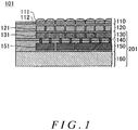
- Fig. 1 is a schematic cross sectional view of an image capturing device 101.
- the image capturing device 101 includes a support substrate 160, a detection processing substrate 150, a detection light receiving substrate 130, a connecting substrate 140, an image-capturing light receiving substrate 120, and an optical element layer 110 which are stacked sequentially from the lower side in the figure.
- the substrates other than the optical element layer 110 are stacked and joined with one another after being manufactured individually by photolithography, respectively.
- the support substrate 160 is a base which remains at the original position after it was used for forming the detection processing substrate 150. However, it may be thinner than it was by grinding and the like, depending on the application. Also, the support substrate 160 may be provided with, for example, a TSV which penetrates therethrough and a bump provided on a lower surface of the support substrate 160 in the figure.
- the detection processing substrate 150 includes a detecting circuit 151 including an element layer, a wiring layer and the like. A plurality of detecting circuits 151 are arranged in a surface direction of the detection processing substrate 150.
- the connecting substrate 140 mechanically couples, and also electrically couples the detection processing substrate 150 immediately under the connecting substrate 140 and the detection light receiving substrate 130 immediately on the connecting substrate 140.
- the connecting substrate 140 may include a passive element embedded therein and used by the detecting circuit 151, such as a capacitative element and a resistor element.
- the detection light receiving substrate 130 includes a plurality of detection light receiving elements 131 to form a photoelectric converting unit.
- Each of the detection light receiving elements 131 receives an incident light which is transmitted through the optical element layer 110 and the image-capturing light receiving substrate 120 and enters the light receiving element, and outputs an electrical signal in accordance with an intensity of the incident light.
- Each of the detection light receiving elements 131 is connected to the detecting circuit 151 of the detection processing substrate 150 through a wiring and elements formed to penetrate through the connecting substrate 140. This allows the electrical signals output from the detection light receiving elements 131 to be input to the detecting circuit 151 of the detection processing substrate 150.
- the image-capturing light receiving substrate 120 includes a plurality of image-capturing light receiving elements 121.
- the optical element layer 110 includes, for example, an on-chip color filter 112 and an on-chip lens 111 to optically process an incident light which enters the image-capturing light receiving elements 121 in advance.
- the optical element layer 110 is formed by stacking and processing optical material after other substrates are stacked.
- Fig. 2 is a schematic plan view of a CMOS sensor unit 129 which includes image-capturing light receiving elements 121 and is formed on the image-capturing light receiving substrate 120.
- the CMOS sensor unit 129 includes a sensor array 122, a column signal processing circuit 123, a horizontal driving circuit 124, and a vertical driving circuit 125 and is operated in response to a control signal fed from the outside.
- the sensor array 122 includes a plurality of image-capturing light receiving elements 121 arrayed in a matrix. Each of the image-capturing light receiving elements 121 forms a unit pixel in an image sensor with a plurality of transistors.
- the vertical driving circuit 125 is provided along one side of columns of the sensor array 122.
- the column signal processing circuit 123 and the horizontal driving circuit 124 are provided along a side orthogonal to the side along which the vertical driving circuit 125 is provided.
- the vertical driving circuit 125 is connected to each row of the image-capturing light receiving elements 121 at one end of a plurality of driving lines provided horizontally in the figure.
- the vertical driving circuit 125 includes a shift register and feeds pulse signals to select a plurality of connected driving lines sequentially and drive the image-capturing light receiving elements 121 to the selected driving line. This allows the image-capturing light receiving elements 121 to be selectively scanned sequentially row by row in a vertical direction.
- the column signal processing circuit 123 includes, for example, a double correlation sampling circuit, a load transistor, and a column selecting transistor, and is connected to the image-capturing light receiving elements 121 for each column.
- the horizontal driving circuit 124 is formed by the shift register, for example, and connected to the column selecting transistor in the column signal processing circuit 123.
- the horizontal driving circuit 124 drives the column selecting transistor of the column signal processing circuit 123 sequentially to selectively scan the image-capturing light receiving elements 121 for each column sequentially through the column signal processing circuit 123.
- the image-capturing light receiving elements 121 selectively driven by the horizontal driving circuit 124 output to the column signal processing circuit 123 voltage signals in accordance with electrical charges accumulated in a floating diffusion layer.
- the column signal processing circuit 123 outputs electrical signals in accordance with the intensity of the incident light entering the image-capturing light receiving elements 121, after removing influences of pattern noises by double correlation sampling. This results in electrical signals reflecting a light image formed on a light receiving surface of the sensor array 122 to be output to an external apparatus such as a storage apparatus and a display apparatus.
- Fig. 3 is a circuit diagram showing a configuration of a modulation signal detecting unit 201 in the image capturing device 101.
- the modulation signal detecting unit 201 includes a modulated light detecting unit 210 and a lock-in amplifying unit 220.
- the modulated light detecting unit 210 includes detection light receiving elements 131 including main pixels 134 and sub pixels 132 provided in the detection light receiving substrate 130, a filter unit 142 provided in the connecting substrate 140, and a pair of transistors 211, 212 provided in the detection processing substrate 150 to detect a modulated light component included in an incident light entering the image capturing device 101.
- the modulated light component has an intensity which varies at a predetermined frequency.
- the sub pixel 132 and the main pixel 134 may be provided in the common detection light receiving substrate 130.
- the sub pixel 132 is formed by photoelectric converting elements such as photodiodes and flows currents in accordance with the intensity of the received incident light.
- the filter unit 142 is formed, for example, by using a parasitic capacitance of a TSV as capacitative elements and connected to the sub pixel 132 at one end, where the TSV is formed to penetrate the connecting substrate 140 which is stacked to electrically connect the detection light receiving substrate 130 and the detection processing substrate 150.
- the filter unit 142 blocks or reduces a preset bandwidth component.
- the filter unit 142 may also include a TSV and elements of a high resistance or a high capacity formed of polysilicon and the like in the connecting substrate 140.
- the drain of one transistor 211 is connected to the other end of the filter unit 142. Also, for the transistor 211, the drain and the gate are shorted.
- the main pixel 134 is formed by photoelectric converting elements such as photodiodes and flows currents in accordance with the intensity of the received incident light.
- the drain of the other transistor 212 is connected to an output of the main pixel 134 and an input of the lock-in amplifying unit 220.
- the gate of the transistor 212 is connected to the gate of one transistor 211. Note that the parasitic capacitance 213 exists between the gates of a pair of transistors 211, 212.
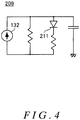
- Fig. 4 is a circuit diagram showing an equivalent circuit of a background light detecting unit 209.
- the background light detecting unit 209 configures a part of the modulated light detecting unit 210 as surrounded by dotted lines shown in Fig. 3 and detects a background light component included in an incident light entering the image capturing device 101.
- the background light component is a light component other than the modulated light component which includes a light component varying at a frequency different from a frequency of the modulated light component.
- the background light component is derived from an environment light fed from a light source such as the sun and lighting fixtures, and includes the one which enters the image capturing device 101 directly from the light source and the one which enters after being reflected on the subject or the like.
- the background light detecting unit 209 is formed to include elements to form the filter unit 142, in addition to the sub pixel 132 and the transistor 211.
- the sub pixel 132 functions as a current source and the transistor 211 forms a current mirror circuit.
- the lock-in amplifying unit 220 in the modulation signal detecting unit 201 of the image capturing device 101 includes an operational amplifier 221, a multiplier 222, and an integrator 223 provided on the detection processing substrate 150.
- the operational amplifier 221 receives an output of the modulated light detecting unit 210 at an inverting input. Also, a non-inverting input and an output of the operational amplifier 221 are coupled by a resistor element. This allows the operational amplifier 221 to be operated as a current-voltage converter.
- the multiplier 222 configures a mixer which multiplies the output of the operational amplifier 221 by a reference signal 224.
- the reference signal 224 input to the multiplier 222 is modulated at the same modulation frequency as the modulation frequency of the modulated light signal to be a detection target.
- the integrator 223 is formed of a low pass filter, for example, and performs an integration processing on the output signal of the multiplier 222. In this manner, in the light signal received by the modulated light detecting unit 210, the modulated light component modulated at the same frequency as the frequency of the reference signal 224, is output from the modulation signal detecting unit 201. This allows a signal of the modulated light component included in the incident light received by the image capturing device 101 to be obtained, on which the phase difference from the reference signal 224 or the amplitude (intensity) is reflected.
- Fig. 5 is a schematic view of an image capturing apparatus 300 including the image capturing device 101.
- the image capturing apparatus 300 includes an image capturing lens 310, a camera body 320, and an irradiating unit 330.
- the image capturing lens 310 is mounted on the camera body 320 which houses the image capturing device 101.
- an image of the subject is formed on an image capturing surface of the CMOS sensor unit 129 in the image-capturing light receiving substrate 120 of the image capturing device 101.
- the image of the subject 390 can be captured by recording an electrical signal output by the CMOS sensor unit 129.
- the image capturing includes at least one of a recording operation of a still image and a recording operation of a motion image of the subject 390.
- the irradiating unit 330 irradiates the subject 390 with a modulated light 331 modulated at a predetermined modulation frequency. After reflected on the subject 390, the modulated light 331 with which the subject 390 is irradiated enters the image capturing device 101 of the image capturing apparatus 300 as a reflected light.
- the image capturing apparatus 300 when the image capturing device 101 receives the modulated light 331 output from the irradiating unit 330, it measures a length of time from when the received modulated light 331 was output from the irradiating unit 330 until it is detected by the modulated light detecting unit 210. This allows for calculation of a distance between the subject 390 and the image capturing device 101. Furthermore, the image capturing apparatus 300 can focus the image capturing lens 310 in accordance with the calculated distance.
- the subject 390 is illuminated by the illumination light 381 output from a lighting fixture 380 in the room. Also, if the image capturing of the subject 390 by the image capturing apparatus 300 is performed in the daytime, the subject 390 is also irradiated with the sunlight directly or indirectly. Therefore, in the image capturing apparatus 300, a background light component of, for example, the illumination light 381 and the sunlight which are different from the component of the modulated light 331 output from the irradiating unit 330 also enters the image capturing device 101.
- the sunlight which may be included in the background light component may vary continuously, even at a period longer than the modulation frequency of the modulated light component.
- the illumination light 381 may also vary periodically in accordance with a frequency of an alternate current source. Furthermore, if something moves around the subject 390, the intensity of the light with which the subject 390 is irradiated varies, even if it is not the light source. Therefore, if the modulation component and the background light component enter the image capturing device 101 together, detection accuracy of the modulated light component by the modulated light detecting unit 210 may be affected.
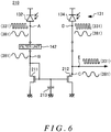
- Fig. 6 is a diagram illustrating an operation of the modulated light detecting unit 210.
- An incident light including the modulated light 331 and a background light such as the illumination light 381 enters a pair of detection light receiving elements 131.
- a current signal flows which varies in accordance with both components of a modulation component corresponding to the modulated light 331 and a background light component corresponding to the illumination light 381.
- the filter unit 142 is connected to the output of the sub pixel 132. Therefore, through the node B connected to the drain of the transistor 211 through the filter unit 142, a current flow having a waveform in which the modulation component is removed or reduced.
- a current from which the modulation component is removed also flows through the node C connected to the drain of the transistor 212. This allows for a current signal having a waveform in which the background light component is reduced or removed being output to a node E branched from between the main pixel 134 and the transistor 212.
- an electrical signal resulting from a current signal corresponding to the modulation component being reduced in a current signal corresponding to the incident light is output in the background light detecting unit 209 which includes the sub pixel 132. Furthermore, the current mirror circuit causes the current signal output by the background light detecting unit 209 to be subtracted from the current signal output by the main pixel 134.
- the lock-in amplifying unit 220 of the modulation signal detecting unit 201 allows a current signal which corresponds to the incident light and from which the background light component corresponding to the background light is removed or reduced to be input to the lock-in amplifying unit 220 of the modulation signal detecting unit 201.
- the light receiving area ratio of the sub pixel 132 and the main pixel 134 and the size ratio of the transistors 211, 212 should be equalized, respectively, in view of the operation of the modulated light detecting unit 210. This allows the background light component to be removed or reduced in the output of the modulated light detecting unit 210 with a high accuracy.
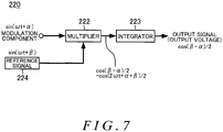
- Fig. 7 is a diagram illustrating an operation of the lock-in amplifying unit 220.
- the background light component is removed or reduced in the input signal to the lock-in amplifying unit 220.
- the modulation component modulated at a modulation frequency ⁇ t of the modulated light 331 is input to the multiplier 222.
- the reference signal 224 input to the multiplier 222 is modulated at the same modulation frequency ⁇ t as the modulated light 331.
- cos ( ⁇ - ⁇ )/2-cos (2 ⁇ t+ ⁇ + ⁇ )/2 is output from the multiplier 222.
- This is processed in the integrator 223 so that a signal corresponding to cos ( ⁇ - ⁇ )/2 is output.
- This varies a signal level of a direct current signal output by the integrator 223 in accordance with a phase difference between the modulated light 331 which enters the modulated light detecting unit 210 and the reference signal 224.
- a travel time of the modulated light 331 from when it was output from the irradiating unit 330 and reflected on the subject 390 until it reaches the image capturing device 101.
- the modulation signal detecting unit 201 of the image capturing device 101 can be used as a range finder to measure a distance between the image capturing device 101 and the subject 390.
- the image capturing lens 310 can be focused based on the output of the modulation signal detecting unit 201.
- the image capturing device 101 can capture an image of the subject 390 with the CMOS sensor unit 129 provided on the image-capturing light receiving substrate 120.
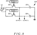
- Fig. 8 is a diagram showing an exemplary circuit of the lock-in amplifying unit 220.
- the illustrated circuit includes a pair of transistors which receives the modulation component detected by the modulated light lock-in amplifying unit 220 at the drain and a pair of capacitative elements connected to the source of each transistor.
- the transistor receives the reference signal 224 at the gate to form the multiplier 222 which multiplies the modulation component by the reference signal.
- the capacitative element functions as a low pass filter to form the integrator 223 which accumulates electrical charges in proportion to an integrated value of the outputs of the multiplier 222.
- a reference signal 1 and a reference signal 2 input to a pair of multipliers 222 are out of phase with each other by 180 degrees.
- electrical charges accumulated in a pair of integrators 223 are read out by a pixel amplifier of a source follower or the like and subtracted so that the phase shifting against the reference signal of the received modulation component is detected.
- Fig. 9 is a diagram illustrating an operation of the lock-in amplifying unit 220 described above.
- the illustrated lock-in amplifying unit 220 includes two systems of the multiplier 222 and the integrator 223 for the modulation component. In a pair of multipliers 222, the reference signal 1 [sin ( ⁇ t)] and the reference signal 2 [cos ( ⁇ t)] orthogonal to each other are multiplied by the modulation component of the incident light.
- [ ⁇ cos (2 ⁇ t+ ⁇ ) + cos ( ⁇ ) ⁇ /2] is output from one multiplier 222 while [ ⁇ sin (2 ⁇ t+ ⁇ ) -sin ( ⁇ ) ⁇ /2] is output from the other multiplier 222, respectively.
- [cos ( ⁇ )/2] and [-sin ( ⁇ )/2] is output from the output of the lock-in amplifying unit 220.
- the lock-in amplifying unit 220 as described above can detect and correct the phase difference between the modulation component of the received incident light and the reference light to increase sensitivity to detect the modulation component of the incident light. Also, it can output the phase difference directly so that load on the computation unit is reduced and a distance to the image capturing target or the like is rapidly calculated.
- the lock-in amplifiers 220 may be provided for each of a plurality of detection light receiving elements 131 or each of a plurality of main pixels 134, individually, or a single lock-in amplifying unit 220 may be provided for a plurality of detection light receiving elements 131 or a plurality of main pixels 134.
- a detecting unit including at least one of the multiplier 222 to which the reference signal 1 is input and the integrator 223 connected to this multiplier 222 and a detecting unit including at least one of the multiplier 222 to which the reference signal 2 is input and the integrator 223 connected to this multiplier 222 may be provided on different substrates stacked one above the other, respectively, or may be provided on the same substrate.
- the lock-in amplifying unit 220 may also include a first system including the detecting unit described above to detect the reflected light of the reference signal 1 reflected on the subject 390 and a second system including the detecting unit described above to detect the reflected light of the reference signal 2 having a modulation frequency different from that of the reference signal 1 and reflected on the subject 390.
- the reference signal 2 has a modulation frequency lower than the reference signal 1. Therefore, the phase shifting of the reflected lights allows the first system and the second system to have different periodicities for calculating the distance between the subject 390 and the image capturing device 101. Given that the distance is detected by the second system with a long period, the first system calculates a distance with a high accuracy, thereby achieving both of a broader scope of an absolute distance to be calculated and accuracy of a distance to be detected.
- the substrate provided with the detecting unit to which the reference signal 1 is input is arranged in a layer closer to the image-capturing light receiving substrate 120 than the substrate provided with the detecting unit to which the reference signal 2 is input having a modulation frequency lower than the modulation frequency of the reference signal 1. Also, these detecting units may also be provided on the same substrate.
- a combination may be selected to uniquely determine n to satisfy an expression of [ ⁇ 2- ⁇ 2 ⁇ n ⁇ 1 ⁇ ⁇ 2+ ⁇ 2] for the first modulation frequency and the second modulation frequency. This allows the distance to the subject 390 from the image capturing device 101 to be determined by one ranging operation so that the ranging operation is completed in a short time.
- each of the reference signal 1 and the reference signal 2 is used for distance detection.
- one of the reference signal 1 and the reference signal 2 may be used for distance detection while the other may be used for forming images.
- two reference signals may be used for forming images, respectively.
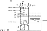
- Fig. 10 is a partial schematic view of another modulation signal detecting unit 202.
- the modulation signal detecting unit 202 has the same structure as the modulation signal detecting unit 201 shown in Fig. 3 , except for the portion described next. Also, the modulation signal detecting unit 202 may be replaced with the modulation signal detecting unit 201 in the image capturing device 101. Thus, the same reference numeral is applied to the common element and redundant description is omitted.
- the modulation signal detecting unit 202 is different from the modulation signal detecting unit 201 in including a plurality of switches 231, 232, 233.
- a first switch 231 is provided between the output of the sub pixel 132 and the output of the main pixel 134 to couple or disconnect both. In the illustrated state, the switch 231 is disconnected.
- a second switch 232 is provided between the output of the sub pixel 132 and the input end of the filter unit 142 to couple or disconnect both. In the illustrated state, the switch 232 is coupled. Note that one end of the first switch 231 is connected to between the sub pixel 132 and the second switch 232. Thus, irrespective of whether the second switch 232 is in an opened or closed state, the one end of the first switch 231 is connected to the output of the sub pixel 132.
- a third switch 233 is provided between the drain and the gate of the transistor 211 to couple or disconnect both. In the illustrated state, the switch 233 is coupled.
- the switches 231, 232, 233 can be opened or closed individually by a control signal.
- the detection light receiving substrate 130 converts the incident light which enters through the image-capturing light receiving substrate 120 to an electrical signal.
- the modulated light 331 output by the irradiating unit 330 should be of a bandwidth which facilitates transmission through the image-capturing light receiving substrate 120.
- the modulated light 331 with which the irradiating unit 330 irradiates the subject 390 may be of an infrared bandwidth.
- the modulated light 331 a light receiving element formed of a compound semiconductor such as InGaAs is used for the main pixel 134 and the sub pixel 132 to improve the sensitivity.
- the detection light receiving substrate 130 may be formed of substrate material different from that of other substrates.
- Fig. 11 is a schematic view showing a different state of the modulation signal detecting unit 202 shown in Fig. 10 .
- the first switch 231 is coupled.
- both of the second switch 232 and the third switch 233 are disconnected.
- both of the sub pixel 132 and the main pixel 134 are connected to the drain of one transistor 212 such that the other transistor 211 is in a state disconnected from any of the sub pixel 132 and the main pixel 134.
- the modulation signal detecting unit 202 as described above is operated as follows. First, the switches 231, 232, 233 are put into the state shown in Fig. 10 , and receive the incident light including the modulation component and the background light component. As described for the modulation signal detecting unit 201, this results in the state in which an electrical signal in which the background light component is removed or reduced is input to the lock-in amplifying unit 220.
- the control signal puts the switches 231, 232, 233 into the state shown in Fig. 11 .
- the parasitic capacitance 213 which exists between the transistors 211, 212 is charged by the background light detecting unit 209. Therefore, even if the transistor 211 is decoupled, the gate voltage of the transistor 212 is clamped, thereby maintaining the state in which the background light component is removed or reduced in the electrical signal input to the lock-in amplifying unit 220.
- the modulation signal detecting unit 202 receives the incident light from both of the sub pixel 132 and the main pixel 134 as a whole, the light receiving area is increased thereby improving the sensitivity.
- switches 231, 232, 233 are connected as in the state shown in Fig. 10 at a predetermined period so that the gate voltage of the transistor 212 is updated and the background light component is removed in accordance with the actual situation.
- the varying period of the background light component is long enough to remove the background light component effectively, regardless of such an intermittent update.
- Fig. 12 is a partial schematic view of another modulation signal detecting unit 203.
- the modulation signal detecting unit 203 has the same structure as the modulation signal detecting unit 201 shown in Fig. 3 , except for the portion described next. Also, the modulation signal detecting unit 203 may be replaced with the modulation signal detecting unit 201 in the image capturing device 101. Thus, the same reference numeral is applied to the common element and redundant description is omitted.
- the modulation signal detecting unit 203 is different from the modulation signal detecting unit 201 in a plurality of main pixels 134 connected to the background light detecting unit 209 including a single sub pixel 132.
- the transistor 212 and the lock-in amplifying unit 220 are connected to each of a plurality of main pixels 134.
- the gate of the transistor 211 of the background light detecting unit 209 is connected to the gate of a plurality of transistors 212.
- exemplary cases are illustrated in which two pixels, the main pixel 134 and the sub pixel 132, are used.
- the sub pixel 132 may not be used.
- electrical signals indicating currents output from the main pixel 134 are converted to a voltage by a current-voltage converting circuit including an op-amp and a resistance, and subsequently electrical signals indicating the voltage are branched. From one of the branched electrical signals, a voltage value is extract corresponding to the background light component via the filter unit such as a low pass filter.
- electrical signals indicating a voltage value corresponding to the modulated light component are extracted, where the voltage value results from a voltage value of signals not via the filter unit, that is, a voltage value including both of the modulated light component and the background light component from which a voltage value corresponding to the background light component is subtracted by using the op-amp.
- Fig. 13 is a schematic view of the modulation signal detecting unit 204.
- the modulation signal detecting unit 204 has the same structure as the modulation signal detecting unit 201 shown in Fig. 3 , except for the portion described next. Also, the modulation signal detecting unit 204 may be replaced with the modulation signal detecting unit 201 in the image capturing device 101. Thus, the same reference numeral is applied to the common element and redundant description is omitted.
- the modulation signal detecting unit 204 includes a single detection light receiving elements 131, a switching unit 136 and a switch 234, instead of the sub pixel 132 and the main pixel 134.
- the switching unit 136 selectively connects the output of the detection light receiving elements 131 to the drain of either the transistor 211 or 212.
- the switch 234 couples or disconnects the drain and the gate of the transistor 211 provided at the side of the background light detecting unit 209.
- the switching unit 136 connects the output of the detection light receiving elements 131 to the transistor 211. Also, the switch 234 makes the drain and the gate of the transistor 211 shorted. Thus, a current from which the modulation component is removed or reduced by the filter unit 142 flows through the transistor 211. As a result, a current in which the modulation component is reduced also flows through the transistor 212 which forms the transistor 211 and the current mirror circuit. Also, the parasitic capacitance 213 between the transistors 211, 212 is charged.
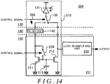
- Fig. 14 is a schematic view showing another state of the modulation signal detecting unit 204.
- the control signal switches the switching unit 136 and the switch 234. This allows the output of the detection light receiving elements 131 to be connected to the input of the lock-in amplifying unit 220 and the drain of the transistor 212. Also, the drain and the gate of the transistor 211 are disconnected. Thus, the filter unit 142 and the transistor 211 are decoupled from the detection light receiving elements 131. However, the parasitic capacitance 213 has already been charged. Therefore, even if the transistor 211 is decoupled, the gate voltage of the transistor 212 is clamped, thereby maintaining the state in which the background light component is removed or reduced in the electrical signal input to the lock-in amplifying unit 220.
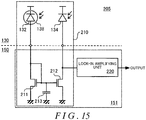
- Fig. 15 is a schematic view of still another modulation signal detecting unit 205.
- the modulation signal detecting unit 205 has the same structure as the modulation signal detecting unit 201 shown in Fig. 3 , except for the portion described next. Also, the modulation signal detecting unit 205 may be replaced with the modulation signal detecting unit 201 in the image capturing device 101. Thus, the same reference numeral is applied to the common element and redundant description is omitted.
- the modulation signal detecting unit 205 is different from the modulation signal detecting unit 201 in the sub pixel 132 including an optical filter 138.
- the optical filter 138 has a characteristic to block or reduce a light having a wavelength of the modulated light component in the incident light entering the sub pixel 132. Thus, the modulated light component has already been reduced in the current signal output from the sub pixel 132 which receives the incident light.
- the filter unit 142 allows the filter unit 142 to be omitted. It should be appreciated that, however, the optical filter 138 and the filter unit 142 which is an electrical filter may also be used in combination. This allows a rapid block characteristic which cannot be obtained from the optical filter 138 or the electrical filter unit 142 alone to reduce the modulated light component.
- the optical filter 138 may be embedded in, for example, an on-chip color filter 112 of the image capturing device 101. Also, the modulated light 331 of a bandwidth to be removed by the on-chip color filter 112 may be used as the modulated light 331.
- a luminous paint may be used which is applied to a member through which the incident modulated light 331 is transmitted.
- the luminous paint substantially works as a low pass filter by accumulating the incident lights of a particular bandwidth.
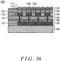
- Fig. 16 is a schematic cross sectional view of another image capturing device 102.
- the image capturing device 102 has the same structure as the image capturing device 101 shown in Fig. 1 , except for the portion described next. Thus, the same reference numeral is applied to the common element and redundant description is omitted.
- the image capturing device 102 is different from the image capturing device 101 in including two detection light receiving substrates 130. Two detection light receiving substrates 130 are stacked one above the other and provided between the image-capturing light receiving substrate 120 and the connecting substrate 140.
- Each of two detection light receiving substrates 130 includes a plurality of detection light receiving elements 131 spaced from one another.
- the arrangement intervals of the detection light receiving elements 131 of each of the detection light receiving substrates 130 are equal to one another. However, the positions of the detection light receiving elements 131 of one detection light receiving substrate 130 are not aligned with those of the other detection light receiving substrate 130. Thus, if two detection light receiving substrates 130 are stacked, each detection light receiving element 131 does not block the incident light to enter the other detection light receiving element 131 so that the detection light receiving elements 131 of the detection light receiving substrate 130 at the lower side in the figure receive the incident lights through the detection light receiving substrate 130 at the upper side in the figure.
- the detection light receiving elements 131 provided in one detection light receiving substrate 130 provided at the upper side in the figure are connected to the detecting circuit 151 of the detection processing substrate 150 as the main pixel 134. Also, the detection light receiving elements 131 provided in the other detection light receiving substrate 130 provided at the lower side in the figure are connected to the detecting circuit 151 of the detection processing substrate 150 as the sub pixel 132. This can improve incident efficiency to the main pixel 134 which contributes detection of the modulated light 331.
- the main pixel 134 as a first photoelectric converting unit and the sub pixel 132 as a second converting unit may be provided on different substrates, respectively, the substrates then may be stacked one above the other, and each pixel may receive the incident light.
- Fig. 17 is a schematic cross sectional view of still another image capturing device 103.
- the image capturing device 103 has the same structure as the image capturing device 101 shown in Fig. 1 , except for the portion described next. Thus, the same reference numeral is applied to the common element and redundant description is omitted.
- the image capturing device 103 has the same structure as the image capturing device 102 shown in Fig. 16 in including two detection light receiving substrates 130. Also, the main pixel 134 is provided in the detection light receiving substrate 130 at the upper side in the figure while the sub pixel 132 is formed in the detection light receiving substrate 130 at the lower side in the figure, which is also the same structure as the image capturing device 102 shown in Fig. 16 .
- the image capturing device 103 is different from the image capturing device 102 in the main pixel 134 and the sub pixel 132 provided approximately adjacent to each other in two detection light receiving substrates 130.
- the main pixel 134 and the sub pixel 132 are arranged to be overlapped in an incident direction of the incident light to be received.
- the main pixel 134 and the sub pixel 132 receive the incident light at the same position with respect to each other.
- the sub pixel 132 may receive the incident light transmitted through the main pixel 134. This results in the main pixel 134 and the sub pixel 132 provided with the same density as the image-capturing light receiving elements 121. Thus, in the image capturing device 103, an image including distance information can be captured for each pixel.
- Fig. 18 is a schematic cross sectional view of another image capturing device 104.
- the image capturing device 104 has the same structure as the image capturing device 103 shown in Fig. 17 , except for the portion described next. Thus, the same reference numeral is applied to the common element and redundant description is omitted.
- each of two detection light receiving substrates 130 includes the sub pixels 132 and the main pixels 134 which are provided alternately. Also, an arrangement of the sub pixels 132 and the main pixels 134 of the upper detection light receiving substrate 130 and that of the lower detection light receiving substrate 130 are shifted by one pixel from each other. This allows in the image capturing device 104, the stacking order of the main pixel 134 and the sub pixel 132 in a vertical direction is switched alternately.
- the main pixel 134 and the sub pixel 132 exist in each of two detection light receiving substrates 130 in a mixed state. Also, in the image capturing device 104, the main pixel 134 and the sub pixel 132 receive the incident light at the same position corresponding to each other. This can resolve imbalance of light receiving efficiency between the sub pixel and the main pixel 134 which results from the sub pixel 132 receiving a light through the main pixel 134.
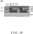
- Fig. 19 is a schematic cross sectional view of another image capturing device 105.
- the image capturing device 105 has the same structure as the image capturing device 101 shown in Fig. 1 , except for the portion described next. Thus, the same reference numeral is applied to the common element and redundant description is omitted.
- the image capturing device 105 is different from the image capturing device 105 in including an integrated light receiving substrate 170 in which the image-capturing light receiving substrate 120 and the detection light receiving substrate 130 are integrated. This can reduce the number of layers of substrates to form the image capturing device 105 and also reduce manufacturing cost.
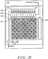
- Fig. 20 is a schematic plan view showing an arrangement of light receiving elements in a CMOS sensor unit 179 formed on the integrated light receiving substrate 170.
- the CMOS sensor unit 179 of the integrated light receiving substrate 170 has the same structure as the CMOS sensor unit 129 shown in Fig. 2 , except for the portion described next.
- the same reference numeral is applied to the common element and redundant description is omitted.
- the image-capturing light receiving elements 121 and the detection light receiving elements 131 including the sub pixels 132 and the main pixels 134 are arrayed repeatedly in one substrate to form a sensor array 122.
- the image-capturing light receiving elements 121 are connected to the column signal processing circuit 123, the horizontal driving circuit 124, and the vertical driving circuit 125 to form a CMOS sensor for image capturing.
- the detection light receiving elements 131 output the outputs of the light receiving elements directly to the detecting circuit 151 of the detection processing substrate 150. Therefore, the detection light receiving elements 131 are not connected to the column signal processing circuit 123, the horizontal driving circuit 124, or the vertical driving circuit 125 on the integrated light receiving substrate 170.
- the sub pixel 132 and the main pixel 134 are dedicated to detecting the modulated light.
- the main pixel 134 can also be used as a part of the image-capturing light receiving elements 121.
- signals from the image-capturing light receiving elements 121 which are the main pixels 134 may be output to both of the image generating unit including a processing circuit to form an image and the detecting unit including the detecting circuit 151, or may be output to the image generating unit and the detecting unit selectively.
- a switching unit may also be provided to switch output destinations from the main pixels 134.
- the image generating unit described above and the detecting unit described above may be provided on different substrates from each other and they are stacked one above the other.
Landscapes
- Engineering & Computer Science (AREA)
- Multimedia (AREA)
- Signal Processing (AREA)
- Solid State Image Pick-Up Elements (AREA)
- Transforming Light Signals Into Electric Signals (AREA)
- Studio Devices (AREA)
- Physics & Mathematics (AREA)
- Electromagnetism (AREA)
Abstract
Description
- The present invention relates to a light detecting apparatus, an image capturing apparatus and an image capturing device.
- There is a circuit which removes background components included in a received light signal by an alternate current connection and inputs the signal to a lock-in amplifier (for example, refer to Patent document 1).
- [Patent document 1] Japanese Translation of PCT International Application Publication No.
2002-502980 - Restrictions on a capacity of a capacitative element which may be used for the alternate current connection may result in an insufficient gain of the amplifier.
- In a first aspect of the present invention, provided is an image capturing device including: a first photoelectric converting unit which outputs a first electrical signal in accordance with an incident light including a modulated light component and a background light component; a second photoelectric converting unit which outputs a second electrical signal resulting from the modulated light component being reduced in the incident light; and a signal processing unit which subtracts the second electrical signal from the first electrical signal to reduce a component corresponding to the background light component in the first electrical signal.
- In a second aspect of the present invention, provided is an image capturing apparatus including: the image capturing device; and an image formation optical system which causes the image capturing device to form an image with an imaging light.
- The summary clause does not necessarily describe all necessary features of the embodiments of the present invention. The present invention may also be a sub-combination of the features described above.
-
-
Fig. 1 is a schematic cross sectional view of an image capturingdevice 101. -
Fig. 2 is a schematic plan view of theCMOS sensor unit 129. -
Fig. 3 is a circuit diagram of the modulationsignal detecting unit 201. -
Fig. 4 is a circuit diagram showing an equivalent circuit of a backgroundlight detecting unit 209. -
Fig. 5 is a schematic view of animage capturing apparatus 300. -
Fig. 6 is a diagram illustrating an operation of the modulatedlight detecting unit 210. -
Fig. 7 is a diagram illustrating an operation of the lock-in amplifyingunit 220. -
Fig. 8 is a diagram showing an exemplary circuit of the lock-in amplifyingunit 220. -
Fig. 9 is a diagram illustrating an operation of the lock-in amplifyingunit 220. -
Fig. 10 is a partial schematic view of another modulationsignal detecting unit 202. -
Fig. 11 is a schematic view showing a different state of the modulationsignal detecting unit 202. -
Fig. 12 is a partial schematic view of another modulationsignal detecting unit 203. -
Fig. 13 is a schematic view of the modulationsignal detecting unit 204. -
Fig. 14 is a schematic view showing another state of the modulationsignal detecting unit 204. -
Fig. 15 is a schematic view of the modulationsignal detecting unit 205. -
Fig. 16 is a schematic cross sectional view of another image capturingdevice 102. -
Fig. 17 is a schematic cross sectional view of another image capturingdevice 103. -
Fig. 18 is a schematic cross sectional view of another image capturingdevice 104. -
Fig. 19 is a schematic cross sectional view of another image capturingdevice 105. -
Fig. 20 is a schematic plan view of aCMOS sensor unit 179. - Hereinafter, some embodiments of the present invention will be described. The embodiments described below are not to limit the claimed invention. All of the combinations of the features described in the embodiments are not necessarily essential for means of the invention.
-
Fig. 1 is a schematic cross sectional view of an image capturingdevice 101. The image capturingdevice 101 includes asupport substrate 160, adetection processing substrate 150, a detectionlight receiving substrate 130, a connectingsubstrate 140, an image-capturinglight receiving substrate 120, and anoptical element layer 110 which are stacked sequentially from the lower side in the figure. The substrates other than theoptical element layer 110 are stacked and joined with one another after being manufactured individually by photolithography, respectively. - The
support substrate 160 is a base which remains at the original position after it was used for forming thedetection processing substrate 150. However, it may be thinner than it was by grinding and the like, depending on the application. Also, thesupport substrate 160 may be provided with, for example, a TSV which penetrates therethrough and a bump provided on a lower surface of thesupport substrate 160 in the figure. - The
detection processing substrate 150 includes a detectingcircuit 151 including an element layer, a wiring layer and the like. A plurality of detectingcircuits 151 are arranged in a surface direction of thedetection processing substrate 150. The connectingsubstrate 140 mechanically couples, and also electrically couples thedetection processing substrate 150 immediately under the connectingsubstrate 140 and the detectionlight receiving substrate 130 immediately on the connectingsubstrate 140. Furthermore, the connectingsubstrate 140 may include a passive element embedded therein and used by the detectingcircuit 151, such as a capacitative element and a resistor element. - The detection
light receiving substrate 130 includes a plurality of detectionlight receiving elements 131 to form a photoelectric converting unit. Each of the detectionlight receiving elements 131 receives an incident light which is transmitted through theoptical element layer 110 and the image-capturinglight receiving substrate 120 and enters the light receiving element, and outputs an electrical signal in accordance with an intensity of the incident light. Each of the detectionlight receiving elements 131 is connected to the detectingcircuit 151 of thedetection processing substrate 150 through a wiring and elements formed to penetrate through the connectingsubstrate 140. This allows the electrical signals output from the detectionlight receiving elements 131 to be input to the detectingcircuit 151 of thedetection processing substrate 150. - The image-capturing
light receiving substrate 120 includes a plurality of image-capturinglight receiving elements 121. When an image is captured by the image capturingdevice 101, an image of the subject is formed on a surface on which the image-capturinglight receiving elements 121 are arrayed. Theoptical element layer 110 includes, for example, an on-chip color filter 112 and an on-chip lens 111 to optically process an incident light which enters the image-capturinglight receiving elements 121 in advance. Theoptical element layer 110 is formed by stacking and processing optical material after other substrates are stacked. -
Fig. 2 is a schematic plan view of aCMOS sensor unit 129 which includes image-capturinglight receiving elements 121 and is formed on the image-capturinglight receiving substrate 120. TheCMOS sensor unit 129 includes asensor array 122, a columnsignal processing circuit 123, ahorizontal driving circuit 124, and avertical driving circuit 125 and is operated in response to a control signal fed from the outside. - The
sensor array 122 includes a plurality of image-capturinglight receiving elements 121 arrayed in a matrix. Each of the image-capturinglight receiving elements 121 forms a unit pixel in an image sensor with a plurality of transistors. - The
vertical driving circuit 125 is provided along one side of columns of thesensor array 122. The columnsignal processing circuit 123 and thehorizontal driving circuit 124 are provided along a side orthogonal to the side along which thevertical driving circuit 125 is provided. Thevertical driving circuit 125 is connected to each row of the image-capturinglight receiving elements 121 at one end of a plurality of driving lines provided horizontally in the figure. - The
vertical driving circuit 125 includes a shift register and feeds pulse signals to select a plurality of connected driving lines sequentially and drive the image-capturinglight receiving elements 121 to the selected driving line. This allows the image-capturinglight receiving elements 121 to be selectively scanned sequentially row by row in a vertical direction. - The column
signal processing circuit 123 includes, for example, a double correlation sampling circuit, a load transistor, and a column selecting transistor, and is connected to the image-capturinglight receiving elements 121 for each column. Thehorizontal driving circuit 124 is formed by the shift register, for example, and connected to the column selecting transistor in the columnsignal processing circuit 123. Thehorizontal driving circuit 124 drives the column selecting transistor of the columnsignal processing circuit 123 sequentially to selectively scan the image-capturinglight receiving elements 121 for each column sequentially through the columnsignal processing circuit 123. - In the row selectively driven by the
vertical driving circuit 125, the image-capturinglight receiving elements 121 selectively driven by thehorizontal driving circuit 124 output to the columnsignal processing circuit 123 voltage signals in accordance with electrical charges accumulated in a floating diffusion layer. The columnsignal processing circuit 123 outputs electrical signals in accordance with the intensity of the incident light entering the image-capturinglight receiving elements 121, after removing influences of pattern noises by double correlation sampling. This results in electrical signals reflecting a light image formed on a light receiving surface of thesensor array 122 to be output to an external apparatus such as a storage apparatus and a display apparatus. -
Fig. 3 is a circuit diagram showing a configuration of a modulationsignal detecting unit 201 in theimage capturing device 101. The modulationsignal detecting unit 201 includes a modulatedlight detecting unit 210 and a lock-inamplifying unit 220. - The modulated
light detecting unit 210 includes detectionlight receiving elements 131 includingmain pixels 134 andsub pixels 132 provided in the detectionlight receiving substrate 130, afilter unit 142 provided in the connectingsubstrate 140, and a pair oftransistors detection processing substrate 150 to detect a modulated light component included in an incident light entering theimage capturing device 101. The modulated light component has an intensity which varies at a predetermined frequency. Thesub pixel 132 and themain pixel 134 may be provided in the common detectionlight receiving substrate 130. - The
sub pixel 132 is formed by photoelectric converting elements such as photodiodes and flows currents in accordance with the intensity of the received incident light. Thefilter unit 142 is formed, for example, by using a parasitic capacitance of a TSV as capacitative elements and connected to thesub pixel 132 at one end, where the TSV is formed to penetrate the connectingsubstrate 140 which is stacked to electrically connect the detectionlight receiving substrate 130 and thedetection processing substrate 150. - The
filter unit 142 blocks or reduces a preset bandwidth component. Thefilter unit 142 may also include a TSV and elements of a high resistance or a high capacity formed of polysilicon and the like in the connectingsubstrate 140. The drain of onetransistor 211 is connected to the other end of thefilter unit 142. Also, for thetransistor 211, the drain and the gate are shorted. - The
main pixel 134 is formed by photoelectric converting elements such as photodiodes and flows currents in accordance with the intensity of the received incident light. The drain of theother transistor 212 is connected to an output of themain pixel 134 and an input of the lock-inamplifying unit 220. Also, the gate of thetransistor 212 is connected to the gate of onetransistor 211. Note that the parasitic capacitance 213 exists between the gates of a pair oftransistors -
Fig. 4 is a circuit diagram showing an equivalent circuit of a backgroundlight detecting unit 209. The backgroundlight detecting unit 209 configures a part of the modulatedlight detecting unit 210 as surrounded by dotted lines shown inFig. 3 and detects a background light component included in an incident light entering theimage capturing device 101. Here, the background light component is a light component other than the modulated light component which includes a light component varying at a frequency different from a frequency of the modulated light component. The background light component is derived from an environment light fed from a light source such as the sun and lighting fixtures, and includes the one which enters theimage capturing device 101 directly from the light source and the one which enters after being reflected on the subject or the like. - The background
light detecting unit 209 is formed to include elements to form thefilter unit 142, in addition to thesub pixel 132 and thetransistor 211. In the backgroundlight detecting unit 209, thesub pixel 132 functions as a current source and thetransistor 211 forms a current mirror circuit. - Referring again to
Fig. 3 , the lock-inamplifying unit 220 in the modulationsignal detecting unit 201 of theimage capturing device 101 includes anoperational amplifier 221, amultiplier 222, and anintegrator 223 provided on thedetection processing substrate 150. Theoperational amplifier 221 receives an output of the modulatedlight detecting unit 210 at an inverting input. Also, a non-inverting input and an output of theoperational amplifier 221 are coupled by a resistor element. This allows theoperational amplifier 221 to be operated as a current-voltage converter. - The
multiplier 222 configures a mixer which multiplies the output of theoperational amplifier 221 by areference signal 224. Thereference signal 224 input to themultiplier 222 is modulated at the same modulation frequency as the modulation frequency of the modulated light signal to be a detection target. Theintegrator 223 is formed of a low pass filter, for example, and performs an integration processing on the output signal of themultiplier 222. In this manner, in the light signal received by the modulatedlight detecting unit 210, the modulated light component modulated at the same frequency as the frequency of thereference signal 224, is output from the modulationsignal detecting unit 201. This allows a signal of the modulated light component included in the incident light received by theimage capturing device 101 to be obtained, on which the phase difference from thereference signal 224 or the amplitude (intensity) is reflected. -
Fig. 5 is a schematic view of animage capturing apparatus 300 including theimage capturing device 101. Theimage capturing apparatus 300 includes animage capturing lens 310, acamera body 320, and anirradiating unit 330. - The
image capturing lens 310 is mounted on thecamera body 320 which houses theimage capturing device 101. When theimage capturing lens 310 is focused to a subject 390, an image of the subject is formed on an image capturing surface of theCMOS sensor unit 129 in the image-capturinglight receiving substrate 120 of theimage capturing device 101. Thus, the image of the subject 390 can be captured by recording an electrical signal output by theCMOS sensor unit 129. Note that the image capturing includes at least one of a recording operation of a still image and a recording operation of a motion image of the subject 390. - The irradiating
unit 330 irradiates the subject 390 with a modulated light 331 modulated at a predetermined modulation frequency. After reflected on the subject 390, the modulated light 331 with which the subject 390 is irradiated enters theimage capturing device 101 of theimage capturing apparatus 300 as a reflected light. - In the
image capturing apparatus 300, when theimage capturing device 101 receives the modulated light 331 output from the irradiatingunit 330, it measures a length of time from when the received modulated light 331 was output from the irradiatingunit 330 until it is detected by the modulatedlight detecting unit 210. This allows for calculation of a distance between the subject 390 and theimage capturing device 101. Furthermore, theimage capturing apparatus 300 can focus theimage capturing lens 310 in accordance with the calculated distance. - Note that in the environment in which the illustrated subject 390 is placed, the subject 390 is illuminated by the
illumination light 381 output from alighting fixture 380 in the room. Also, if the image capturing of the subject 390 by theimage capturing apparatus 300 is performed in the daytime, the subject 390 is also irradiated with the sunlight directly or indirectly. Therefore, in theimage capturing apparatus 300, a background light component of, for example, theillumination light 381 and the sunlight which are different from the component of the modulated light 331 output from the irradiatingunit 330 also enters theimage capturing device 101. - Here, the sunlight which may be included in the background light component may vary continuously, even at a period longer than the modulation frequency of the modulated light component. Also, the
illumination light 381 may also vary periodically in accordance with a frequency of an alternate current source. Furthermore, if something moves around the subject 390, the intensity of the light with which the subject 390 is irradiated varies, even if it is not the light source. Therefore, if the modulation component and the background light component enter theimage capturing device 101 together, detection accuracy of the modulated light component by the modulatedlight detecting unit 210 may be affected. -
Fig. 6 is a diagram illustrating an operation of the modulatedlight detecting unit 210. An incident light including the modulatedlight 331 and a background light such as theillumination light 381 enters a pair of detectionlight receiving elements 131. Thus, through a node A and a node D shown in the figure, a current signal flows which varies in accordance with both components of a modulation component corresponding to the modulatedlight 331 and a background light component corresponding to theillumination light 381. - The
filter unit 142 is connected to the output of thesub pixel 132. Therefore, through the node B connected to the drain of thetransistor 211 through thefilter unit 142, a current flow having a waveform in which the modulation component is removed or reduced. - Because a pair of
transistors transistor 212. This allows for a current signal having a waveform in which the background light component is reduced or removed being output to a node E branched from between themain pixel 134 and thetransistor 212. - In this manner, in the modulated
light detecting unit 210 of theimage capturing device 101, an electrical signal resulting from a current signal corresponding to the modulation component being reduced in a current signal corresponding to the incident light is output in the backgroundlight detecting unit 209 which includes thesub pixel 132. Furthermore, the current mirror circuit causes the current signal output by the backgroundlight detecting unit 209 to be subtracted from the current signal output by themain pixel 134. - This allows a current signal which corresponds to the incident light and from which the background light component corresponding to the background light is removed or reduced to be input to the lock-in
amplifying unit 220 of the modulationsignal detecting unit 201. Note that it is preferable that the light receiving area ratio of thesub pixel 132 and themain pixel 134 and the size ratio of thetransistors light detecting unit 210. This allows the background light component to be removed or reduced in the output of the modulatedlight detecting unit 210 with a high accuracy. -
Fig. 7 is a diagram illustrating an operation of the lock-inamplifying unit 220. As described above, the background light component is removed or reduced in the input signal to the lock-inamplifying unit 220. Thus, the modulation component modulated at a modulation frequency ωt of the modulatedlight 331 is input to themultiplier 222. - The
reference signal 224 input to themultiplier 222 is modulated at the same modulation frequency ωt as the modulatedlight 331. Thus, cos (β-α)/2-cos (2ωt+α+β)/2 is output from themultiplier 222. This is processed in theintegrator 223 so that a signal corresponding to cos (α-β)/2 is output. - This varies a signal level of a direct current signal output by the
integrator 223 in accordance with a phase difference between the modulated light 331 which enters the modulatedlight detecting unit 210 and thereference signal 224. Thus, based on the phase difference corresponding to the signal level, it is possible to calculate a travel time of the modulated light 331 from when it was output from the irradiatingunit 330 and reflected on the subject 390 until it reaches theimage capturing device 101. - In this manner, the modulation
signal detecting unit 201 of theimage capturing device 101 can be used as a range finder to measure a distance between theimage capturing device 101 and the subject 390. Thus, in theimage capturing apparatus 300, theimage capturing lens 310 can be focused based on the output of the modulationsignal detecting unit 201. Furthermore, theimage capturing device 101 can capture an image of the subject 390 with theCMOS sensor unit 129 provided on the image-capturinglight receiving substrate 120. -
Fig. 8 is a diagram showing an exemplary circuit of the lock-inamplifying unit 220. The illustrated circuit includes a pair of transistors which receives the modulation component detected by the modulated light lock-inamplifying unit 220 at the drain and a pair of capacitative elements connected to the source of each transistor. The transistor receives thereference signal 224 at the gate to form themultiplier 222 which multiplies the modulation component by the reference signal. The capacitative element functions as a low pass filter to form theintegrator 223 which accumulates electrical charges in proportion to an integrated value of the outputs of themultiplier 222. - Here, a
reference signal 1 and areference signal 2 input to a pair ofmultipliers 222 are out of phase with each other by 180 degrees. Thus, electrical charges accumulated in a pair ofintegrators 223 are read out by a pixel amplifier of a source follower or the like and subtracted so that the phase shifting against the reference signal of the received modulation component is detected. This allows the illustrated lock-inamplifying unit 220 to detect the phase difference of the modulation component against the reference signal synchronized to the modulation component. -
Fig. 9 is a diagram illustrating an operation of the lock-inamplifying unit 220 described above. The illustrated lock-inamplifying unit 220 includes two systems of themultiplier 222 and theintegrator 223 for the modulation component. In a pair ofmultipliers 222, the reference signal 1 [sin (ωt)] and the reference signal 2 [cos (ωt)] orthogonal to each other are multiplied by the modulation component of the incident light. - [{cos (2ωt+α) + cos (α)}/2] is output from one
multiplier 222 while [{sin (2ωt+α) -sin (α)}/2] is output from theother multiplier 222, respectively. As an integration processing id performed on each output by an integration processing of theintegrator 223, [cos (α)/2] and [-sin (α)/2] is output from the output of the lock-inamplifying unit 220. By calculating tan (α) from these values, the phase difference of the reference signal for the modulate signal is directly calculated. - The lock-in
amplifying unit 220 as described above can detect and correct the phase difference between the modulation component of the received incident light and the reference light to increase sensitivity to detect the modulation component of the incident light. Also, it can output the phase difference directly so that load on the computation unit is reduced and a distance to the image capturing target or the like is rapidly calculated. Note that the lock-inamplifiers 220 may be provided for each of a plurality of detectionlight receiving elements 131 or each of a plurality ofmain pixels 134, individually, or a single lock-inamplifying unit 220 may be provided for a plurality of detectionlight receiving elements 131 or a plurality ofmain pixels 134. - In the example in
Fig. 9 , a detecting unit including at least one of themultiplier 222 to which thereference signal 1 is input and theintegrator 223 connected to thismultiplier 222 and a detecting unit including at least one of themultiplier 222 to which thereference signal 2 is input and theintegrator 223 connected to thismultiplier 222 may be provided on different substrates stacked one above the other, respectively, or may be provided on the same substrate. - Also, in the example in
Fig. 9 , the lock-inamplifying unit 220 may also include a first system including the detecting unit described above to detect the reflected light of thereference signal 1 reflected on the subject 390 and a second system including the detecting unit described above to detect the reflected light of thereference signal 2 having a modulation frequency different from that of thereference signal 1 and reflected on the subject 390. For example, thereference signal 2 has a modulation frequency lower than thereference signal 1. Therefore, the phase shifting of the reflected lights allows the first system and the second system to have different periodicities for calculating the distance between the subject 390 and theimage capturing device 101. Given that the distance is detected by the second system with a long period, the first system calculates a distance with a high accuracy, thereby achieving both of a broader scope of an absolute distance to be calculated and accuracy of a distance to be detected. - If two detecting units are provided on different substrates stacked one above the other, the substrate provided with the detecting unit to which the
reference signal 1 is input is arranged in a layer closer to the image-capturinglight receiving substrate 120 than the substrate provided with the detecting unit to which thereference signal 2 is input having a modulation frequency lower than the modulation frequency of thereference signal 1. Also, these detecting units may also be provided on the same substrate. - Furthermore, where a wavelength of the modulation component of the
reference signal 1 is λ1, a ranging accuracy of the first modulation component by thereference signal 1 is δ2, a ranging value of the second modulation component by thereference signal 2 is Δ2, and an arbitrary positive integer is n, a combination may be selected to uniquely determine n to satisfy an expression of [Δ2-δ2 < nλ1 < Δ2+δ2] for the first modulation frequency and the second modulation frequency. This allows the distance to the subject 390 from theimage capturing device 101 to be determined by one ranging operation so that the ranging operation is completed in a short time. - Also, in the example described above, an exemplary case is illustrated in which each of the
reference signal 1 and thereference signal 2 is used for distance detection. Instead, one of thereference signal 1 and thereference signal 2 may be used for distance detection while the other may be used for forming images. Alternatively, two reference signals may be used for forming images, respectively. -
Fig. 10 is a partial schematic view of another modulationsignal detecting unit 202. The modulationsignal detecting unit 202 has the same structure as the modulationsignal detecting unit 201 shown inFig. 3 , except for the portion described next. Also, the modulationsignal detecting unit 202 may be replaced with the modulationsignal detecting unit 201 in theimage capturing device 101. Thus, the same reference numeral is applied to the common element and redundant description is omitted. - The modulation
signal detecting unit 202 is different from the modulationsignal detecting unit 201 in including a plurality ofswitches first switch 231 is provided between the output of thesub pixel 132 and the output of themain pixel 134 to couple or disconnect both. In the illustrated state, theswitch 231 is disconnected. - A
second switch 232 is provided between the output of thesub pixel 132 and the input end of thefilter unit 142 to couple or disconnect both. In the illustrated state, theswitch 232 is coupled. Note that one end of thefirst switch 231 is connected to between thesub pixel 132 and thesecond switch 232. Thus, irrespective of whether thesecond switch 232 is in an opened or closed state, the one end of thefirst switch 231 is connected to the output of thesub pixel 132. - A
third switch 233 is provided between the drain and the gate of thetransistor 211 to couple or disconnect both. In the illustrated state, theswitch 233 is coupled. Theswitches - If the
switches signal detecting unit 202 is connected in the same manner as the modulationsignal detecting unit 201 shown inFig. 3 . Thus, the modulationsignal detecting unit 202 is operated absolutely the same as the modulationsignal detecting unit 201. - Note that in the
image capturing device 101, the detectionlight receiving substrate 130 converts the incident light which enters through the image-capturinglight receiving substrate 120 to an electrical signal. Thus, in theimage capturing apparatus 300, it is preferable that the modulated light 331 output by the irradiatingunit 330 should be of a bandwidth which facilitates transmission through the image-capturinglight receiving substrate 120. In this regard, the modulated light 331 with which theirradiating unit 330 irradiates the subject 390 may be of an infrared bandwidth. - Also, if an infrared light is used as the modulated
light 331, a light receiving element formed of a compound semiconductor such as InGaAs is used for themain pixel 134 and thesub pixel 132 to improve the sensitivity. As describe above, as theimage capturing device 101 is formed by stacking thesupport substrate 160, thedetection processing substrate 150, the detectionlight receiving substrate 130, the connectingsubstrate 140, the image-capturinglight receiving substrate 120, and theoptical element layer 110 which are individually prepared, the detectionlight receiving substrate 130 may be formed of substrate material different from that of other substrates. -
Fig. 11 is a schematic view showing a different state of the modulationsignal detecting unit 202 shown inFig. 10 . In the illustrated state, thefirst switch 231 is coupled. Also, both of thesecond switch 232 and thethird switch 233 are disconnected. - As a result, in the illustrated modulation
signal detecting unit 202, both of thesub pixel 132 and themain pixel 134 are connected to the drain of onetransistor 212 such that theother transistor 211 is in a state disconnected from any of thesub pixel 132 and themain pixel 134. - The modulation
signal detecting unit 202 as described above is operated as follows. First, theswitches Fig. 10 , and receive the incident light including the modulation component and the background light component. As described for the modulationsignal detecting unit 201, this results in the state in which an electrical signal in which the background light component is removed or reduced is input to the lock-inamplifying unit 220. - Next, the control signal puts the
switches Fig. 11 . In this state, the parasitic capacitance 213 which exists between thetransistors light detecting unit 209. Therefore, even if thetransistor 211 is decoupled, the gate voltage of thetransistor 212 is clamped, thereby maintaining the state in which the background light component is removed or reduced in the electrical signal input to the lock-inamplifying unit 220. On the other hand, because the modulationsignal detecting unit 202 receives the incident light from both of thesub pixel 132 and themain pixel 134 as a whole, the light receiving area is increased thereby improving the sensitivity. - Note that the
switches Fig. 10 at a predetermined period so that the gate voltage of thetransistor 212 is updated and the background light component is removed in accordance with the actual situation. The varying period of the background light component is long enough to remove the background light component effectively, regardless of such an intermittent update. -
Fig. 12 is a partial schematic view of another modulationsignal detecting unit 203. The modulationsignal detecting unit 203 has the same structure as the modulationsignal detecting unit 201 shown inFig. 3 , except for the portion described next. Also, the modulationsignal detecting unit 203 may be replaced with the modulationsignal detecting unit 201 in theimage capturing device 101. Thus, the same reference numeral is applied to the common element and redundant description is omitted. - The modulation
signal detecting unit 203 is different from the modulationsignal detecting unit 201 in a plurality ofmain pixels 134 connected to the backgroundlight detecting unit 209 including asingle sub pixel 132. Thetransistor 212 and the lock-inamplifying unit 220 are connected to each of a plurality ofmain pixels 134. The gate of thetransistor 211 of the backgroundlight detecting unit 209 is connected to the gate of a plurality oftransistors 212. As a result, in theimage capturing device 101 as a whole, the number of backgroundlight detecting units 209 can be reduced, thereby reducing the circuit scale of thedetection processing substrate 150. - In the examples shown in
Fig. 3 to Fig. 11 , exemplary cases are illustrated in which two pixels, themain pixel 134 and thesub pixel 132, are used. However, thesub pixel 132 may not be used. In this case, electrical signals indicating currents output from themain pixel 134 are converted to a voltage by a current-voltage converting circuit including an op-amp and a resistance, and subsequently electrical signals indicating the voltage are branched. From one of the branched electrical signals, a voltage value is extract corresponding to the background light component via the filter unit such as a low pass filter. From the other of the branched electrical signals, electrical signals indicating a voltage value corresponding to the modulated light component are extracted, where the voltage value results from a voltage value of signals not via the filter unit, that is, a voltage value including both of the modulated light component and the background light component from which a voltage value corresponding to the background light component is subtracted by using the op-amp. -
Fig. 13 is a schematic view of the modulationsignal detecting unit 204. The modulationsignal detecting unit 204 has the same structure as the modulationsignal detecting unit 201 shown inFig. 3 , except for the portion described next. Also, the modulationsignal detecting unit 204 may be replaced with the modulationsignal detecting unit 201 in theimage capturing device 101. Thus, the same reference numeral is applied to the common element and redundant description is omitted. - The modulation
signal detecting unit 204 includes a single detectionlight receiving elements 131, aswitching unit 136 and aswitch 234, instead of thesub pixel 132 and themain pixel 134. Theswitching unit 136 selectively connects the output of the detectionlight receiving elements 131 to the drain of either thetransistor switch 234 couples or disconnects the drain and the gate of thetransistor 211 provided at the side of the backgroundlight detecting unit 209. - In the illustrated state, the
switching unit 136 connects the output of the detectionlight receiving elements 131 to thetransistor 211. Also, theswitch 234 makes the drain and the gate of thetransistor 211 shorted. Thus, a current from which the modulation component is removed or reduced by thefilter unit 142 flows through thetransistor 211. As a result, a current in which the modulation component is reduced also flows through thetransistor 212 which forms thetransistor 211 and the current mirror circuit. Also, the parasitic capacitance 213 between thetransistors -
Fig. 14 is a schematic view showing another state of the modulationsignal detecting unit 204. In the illustrated state following the state shown inFig. 13 , the control signal switches theswitching unit 136 and theswitch 234. This allows the output of the detectionlight receiving elements 131 to be connected to the input of the lock-inamplifying unit 220 and the drain of thetransistor 212. Also, the drain and the gate of thetransistor 211 are disconnected. Thus, thefilter unit 142 and thetransistor 211 are decoupled from the detectionlight receiving elements 131. However, the parasitic capacitance 213 has already been charged. Therefore, even if thetransistor 211 is decoupled, the gate voltage of thetransistor 212 is clamped, thereby maintaining the state in which the background light component is removed or reduced in the electrical signal input to the lock-inamplifying unit 220. -
Fig. 15 is a schematic view of still another modulationsignal detecting unit 205. The modulationsignal detecting unit 205 has the same structure as the modulationsignal detecting unit 201 shown inFig. 3 , except for the portion described next. Also, the modulationsignal detecting unit 205 may be replaced with the modulationsignal detecting unit 201 in theimage capturing device 101. Thus, the same reference numeral is applied to the common element and redundant description is omitted. - The modulation
signal detecting unit 205 is different from the modulationsignal detecting unit 201 in thesub pixel 132 including anoptical filter 138. Theoptical filter 138 has a characteristic to block or reduce a light having a wavelength of the modulated light component in the incident light entering thesub pixel 132. Thus, the modulated light component has already been reduced in the current signal output from thesub pixel 132 which receives the incident light. - This allows the
filter unit 142 to be omitted. It should be appreciated that, however, theoptical filter 138 and thefilter unit 142 which is an electrical filter may also be used in combination. This allows a rapid block characteristic which cannot be obtained from theoptical filter 138 or theelectrical filter unit 142 alone to reduce the modulated light component. - The
optical filter 138 may be embedded in, for example, an on-chip color filter 112 of theimage capturing device 101. Also, the modulatedlight 331 of a bandwidth to be removed by the on-chip color filter 112 may be used as the modulatedlight 331. - Also, as the optical filter, a luminous paint may be used which is applied to a member through which the incident modulated light 331 is transmitted. The luminous paint substantially works as a low pass filter by accumulating the incident lights of a particular bandwidth.
-
Fig. 16 is a schematic cross sectional view of anotherimage capturing device 102. Theimage capturing device 102 has the same structure as theimage capturing device 101 shown inFig. 1 , except for the portion described next. Thus, the same reference numeral is applied to the common element and redundant description is omitted. - The
image capturing device 102 is different from theimage capturing device 101 in including two detectionlight receiving substrates 130. Two detectionlight receiving substrates 130 are stacked one above the other and provided between the image-capturinglight receiving substrate 120 and the connectingsubstrate 140. - Each of two detection
light receiving substrates 130 includes a plurality of detectionlight receiving elements 131 spaced from one another. The arrangement intervals of the detectionlight receiving elements 131 of each of the detectionlight receiving substrates 130 are equal to one another. However, the positions of the detectionlight receiving elements 131 of one detectionlight receiving substrate 130 are not aligned with those of the other detectionlight receiving substrate 130. Thus, if two detectionlight receiving substrates 130 are stacked, each detectionlight receiving element 131 does not block the incident light to enter the other detectionlight receiving element 131 so that the detectionlight receiving elements 131 of the detectionlight receiving substrate 130 at the lower side in the figure receive the incident lights through the detectionlight receiving substrate 130 at the upper side in the figure. - In the
image capturing device 102, the detectionlight receiving elements 131 provided in one detectionlight receiving substrate 130 provided at the upper side in the figure are connected to the detectingcircuit 151 of thedetection processing substrate 150 as themain pixel 134. Also, the detectionlight receiving elements 131 provided in the other detectionlight receiving substrate 130 provided at the lower side in the figure are connected to the detectingcircuit 151 of thedetection processing substrate 150 as thesub pixel 132. This can improve incident efficiency to themain pixel 134 which contributes detection of the modulatedlight 331. - In this manner, in the
image capturing device 102, themain pixel 134 as a first photoelectric converting unit and thesub pixel 132 as a second converting unit may be provided on different substrates, respectively, the substrates then may be stacked one above the other, and each pixel may receive the incident light. -
Fig. 17 is a schematic cross sectional view of still anotherimage capturing device 103. Theimage capturing device 103 has the same structure as theimage capturing device 101 shown inFig. 1 , except for the portion described next. Thus, the same reference numeral is applied to the common element and redundant description is omitted. - The
image capturing device 103 has the same structure as theimage capturing device 102 shown inFig. 16 in including two detectionlight receiving substrates 130. Also, themain pixel 134 is provided in the detectionlight receiving substrate 130 at the upper side in the figure while thesub pixel 132 is formed in the detectionlight receiving substrate 130 at the lower side in the figure, which is also the same structure as theimage capturing device 102 shown inFig. 16 . - On the other hand, the
image capturing device 103 is different from theimage capturing device 102 in themain pixel 134 and thesub pixel 132 provided approximately adjacent to each other in two detectionlight receiving substrates 130. As a result, in theimage capturing device 103, themain pixel 134 and thesub pixel 132 are arranged to be overlapped in an incident direction of the incident light to be received. Thus, themain pixel 134 and thesub pixel 132 receive the incident light at the same position with respect to each other. - In this manner, in the
image capturing device 103, thesub pixel 132 may receive the incident light transmitted through themain pixel 134. This results in themain pixel 134 and thesub pixel 132 provided with the same density as the image-capturinglight receiving elements 121. Thus, in theimage capturing device 103, an image including distance information can be captured for each pixel. -
Fig. 18 is a schematic cross sectional view of anotherimage capturing device 104. Theimage capturing device 104 has the same structure as theimage capturing device 103 shown inFig. 17 , except for the portion described next. Thus, the same reference numeral is applied to the common element and redundant description is omitted. - In the
image capturing device 104, each of two detectionlight receiving substrates 130 includes thesub pixels 132 and themain pixels 134 which are provided alternately. Also, an arrangement of thesub pixels 132 and themain pixels 134 of the upper detectionlight receiving substrate 130 and that of the lower detectionlight receiving substrate 130 are shifted by one pixel from each other. This allows in theimage capturing device 104, the stacking order of themain pixel 134 and thesub pixel 132 in a vertical direction is switched alternately. - In this manner, in the
image capturing device 104, themain pixel 134 and thesub pixel 132 exist in each of two detectionlight receiving substrates 130 in a mixed state. Also, in theimage capturing device 104, themain pixel 134 and thesub pixel 132 receive the incident light at the same position corresponding to each other. This can resolve imbalance of light receiving efficiency between the sub pixel and themain pixel 134 which results from thesub pixel 132 receiving a light through themain pixel 134. -
Fig. 19 is a schematic cross sectional view of anotherimage capturing device 105. Theimage capturing device 105 has the same structure as theimage capturing device 101 shown inFig. 1 , except for the portion described next. Thus, the same reference numeral is applied to the common element and redundant description is omitted. - The
image capturing device 105 is different from theimage capturing device 105 in including an integratedlight receiving substrate 170 in which the image-capturinglight receiving substrate 120 and the detectionlight receiving substrate 130 are integrated. This can reduce the number of layers of substrates to form theimage capturing device 105 and also reduce manufacturing cost. -
Fig. 20 is a schematic plan view showing an arrangement of light receiving elements in aCMOS sensor unit 179 formed on the integratedlight receiving substrate 170. Note that theCMOS sensor unit 179 of the integratedlight receiving substrate 170 has the same structure as theCMOS sensor unit 129 shown inFig. 2 , except for the portion described next. Thus, the same reference numeral is applied to the common element and redundant description is omitted. - In the
CMOS sensor unit 179 of the integratedlight receiving substrate 170, the image-capturinglight receiving elements 121 and the detectionlight receiving elements 131 including thesub pixels 132 and themain pixels 134 are arrayed repeatedly in one substrate to form asensor array 122. Here, the image-capturinglight receiving elements 121 are connected to the columnsignal processing circuit 123, thehorizontal driving circuit 124, and thevertical driving circuit 125 to form a CMOS sensor for image capturing. - On the other hand, the detection
light receiving elements 131 output the outputs of the light receiving elements directly to the detectingcircuit 151 of thedetection processing substrate 150. Therefore, the detectionlight receiving elements 131 are not connected to the columnsignal processing circuit 123, thehorizontal driving circuit 124, or thevertical driving circuit 125 on the integratedlight receiving substrate 170. - Note that in the example described above, the
sub pixel 132 and themain pixel 134 are dedicated to detecting the modulated light. However, by switching connection of the gate from being connected to themain pixel 134 in the modulatedlight detecting unit 210 to the GND voltage and switching thereference signal 224 of the lock-inamplifying unit 220 to the direct current voltage, themain pixel 134 can also be used as a part of the image-capturinglight receiving elements 121. - In this case, signals from the image-capturing
light receiving elements 121 which are themain pixels 134 may be output to both of the image generating unit including a processing circuit to form an image and the detecting unit including the detectingcircuit 151, or may be output to the image generating unit and the detecting unit selectively. A switching unit may also be provided to switch output destinations from themain pixels 134. Also, the image generating unit described above and the detecting unit described above may be provided on different substrates from each other and they are stacked one above the other. - While the embodiments of the present invention have been described, the technical scope of the invention is not limited to the above described embodiments. It is apparent to persons skilled in the art that various alterations and improvements can be added to the above-described embodiments. It is also apparent from the scope of the claims that the embodiments added with such alterations or improvements can be included in the technical scope of the invention.
- The operations, procedures, steps, and stages of each process performed by an apparatus, system, program, and method shown in the claims, embodiments, or diagrams can be performed in any order as long as the order is not indicated by "prior to," "before," or the like and as long as the output from a previous process is not used in a later process. Even if the process flow is described using phrases such as "first" or "next" in the claims, embodiments, or diagrams, it does not necessarily mean that the process must be performed in this order.
-
- 101, 102, 103, 104, 105: image capturing device, 110: optical element layer, 111: on-chip lens, 112: on-chip color filter, 120: image-capturing light receiving substrate, 121: image-capturing light receiving element, 122: sensor array, 123: column signal processing circuit, 124: horizontal driving circuit, 125: vertical driving circuit, 129, 179: CMOS sensor unit, 130: detection light receiving substrate, 131: detection light receiving element, 132: sub pixel, 134: main pixel, 136: switching unit, 138: optical filter, 140: connecting substrate, 142: filter unit, 150: detection processing substrate, 151: detecting circuit, 160: support substrate, 170: integrated light receiving substrate, 201, 202, 203, 204, 205: modulation signal detecting unit, 209: background light detecting unit, 210: modulated light detecting unit, 211, 212: transistor, 213: parasitic capacitance, 220: lock-in amplifying unit, 221: operational amplifier, 222: multiplier, 223: integrator, 224: reference signal, 231, 232, 233, 234: switch, 300: image capturing apparatus, 310: image capturing lens, 320: camera body, 330: irradiating unit, 331: modulated light, 381: illumination light, 380: lighting fixture, 390: subject
Claims (20)
- A light detecting apparatus comprising:a photoelectric converting unit which outputs a first electrical signal in accordance with an incident light including a modulated light component and a background light component;a filter unit which outputs a second electrical signal resulting from a signal corresponding to the modulated light component being attenuated in the first electrical signal; anda signal processing unit which subtracts the second electrical signal from the first electrical signal to reduce a signal corresponding to the background light component in the first electrical signal.
- The light detecting apparatus according to claim 1, whereinthe photoelectric converting unit includes a first photoelectric converting element and a second photoelectric converting element each of which outputs the first electrical signal,the filter unit attenuates the signal corresponding to the modulated light component in the first electrical signal output from the second photoelectric converting element, andthe signal processing unit subtracts the second electrical signal from the first electrical signal output from the first photoelectric converting element.
- The light detecting apparatus according to claim 2, comprising:a first substrate provided with the second photoelectric converting element; anda second substrate stacked on the first substrate and provided with the signal processing unit, whereinthe filter unit is electrically connected to the second photoelectric converting element, and includes a capacitative element formed on at least one of the first substrate and the second substrate.
- The light detecting apparatus according to claim 3, wherein the first substrate includes a light receiving substrate provided with the second photoelectric converting element and a connecting substrate stacked on the light receiving substrate, wherein the capacitative element is provided to penetrate through the connecting substrate.
- The light detecting apparatus according to any one of claims 2 to 4, wherein the first photoelectric converting element and the second photoelectric converting element are provided on a common substrate.
- The light detecting apparatus according to any one of claims 2 to 5, comprising a first substrate provided with the first photoelectric converting element and a third substrate stacked on the first substrate and provided with the second photoelectric converting element.
- The light detecting apparatus according to claim 6, wherein the second photoelectric converting element receives the incident light through the first substrate.
- The light detecting apparatus according to claim 6, wherein the second photoelectric converting element receives the incident light through the first photoelectric converting element.
- The light detecting apparatus according to any one of claims 1 to 8, comprising:a first substrate on which a first photoelectric converting element receiving the incident light in the photoelectric converting unit and a second photoelectric converting element receiving the incident light in the filter unit are provided in common; anda second substrate on which the first photoelectric converting element receiving the incident light in the photoelectric converting unit and the second photoelectric converting element receiving the incident light in the filter unit are provided in common, and which is stacked on the first substrate.
- The light detecting apparatus according to claim 9, whereinthe second photoelectric converting element of the second substrate is provided at a position corresponding to the first photoelectric converting element of the first substrate, andthe first photoelectric converting element of the second substrate is provided at a position corresponding to the second photoelectric converting element of the first substrate.
- The light detecting apparatus according to any one of claims 1 to 10, whereinthe first electrical signal and the second electrical signal are current signals, respectively, andthe signal processing unit subtracts a current value of the second electrical signal from a current value of the first electrical signal.
- The light detecting apparatus according to claim 11, wherein the signal processing unit includes a current mirror circuit having a first transistor electrically connected to the photoelectric converting unit and a second transistor electrically connected to the filter unit.
- The light detecting apparatus according to any one of claims 1 to 12, wherein the filter unit includes an optical filter which optically reduces the modulated light component entering the filter unit.
- The light detecting apparatus according to claim 1, comprising a switching unit which selectively connects the photoelectric converting unit to either a wiring connected to the signal processing unit via the filter unit or a wiring connected to the signal processing unit not via the filter unit.
- A light detecting apparatus comprising:a photoelectric converting unit which outputs a first electrical signal in accordance with an incident light including a modulated light component and a background light component;a filter unit which outputs a second electrical signal resulting from the modulated light component being reduced in the incident light; anda signal processing unit which subtracts the second electrical signal from the first electrical signal to reduce a component corresponding to the background light component in the first electrical signal.
- The light detecting apparatus according to claim 16, wherein the filter unit includes a filter which electrically reduces a component corresponding to the modulated light component in the incident light.
- The light detecting apparatus according to claim 15, wherein the filter unit includes an optical filter which optically reduces the modulated light component entering the filter unit.
- An image capturing apparatus comprising the light detecting apparatus according to any one of claims 1 to 17 and an image formation optical system which causes the light detecting apparatus to form an image with an imaging light.
- An image capturing device comprising:a photoelectric converting unit which outputs a first electrical signal in accordance with an incident light including a modulated light component and a background light component; anda filter unit which outputs a second electrical signal resulting from a signal corresponding to the modulated light component being attenuated in the first electrical signal.
- An image capturing device comprising:a photoelectric converting unit which outputs a first electrical signal in accordance with an incident light including a modulated light component and a background light component; anda filter unit which outputs a second electrical signal resulting from the modulated light component being reduced in the incident light.
Applications Claiming Priority (2)
| Application Number | Priority Date | Filing Date | Title |
|---|---|---|---|
| JP2014228475 | 2014-11-10 | ||
| PCT/JP2015/081646 WO2016076328A1 (en) | 2014-11-10 | 2015-11-10 | Light detection device, image-capturing device, and image-capturing element |
Publications (2)
| Publication Number | Publication Date |
|---|---|
| EP3220627A1 true EP3220627A1 (en) | 2017-09-20 |
| EP3220627A4 EP3220627A4 (en) | 2018-04-25 |
Family
ID=55954411
Family Applications (1)
| Application Number | Title | Priority Date | Filing Date |
|---|---|---|---|
| EP15858779.0A Withdrawn EP3220627A4 (en) | 2014-11-10 | 2015-11-10 | Light detection device, image-capturing device, and image-capturing element |
Country Status (5)
| Country | Link |
|---|---|
| US (1) | US10182190B2 (en) |
| EP (1) | EP3220627A4 (en) |
| JP (1) | JP6451746B2 (en) |
| CN (1) | CN107079122B (en) |
| WO (1) | WO2016076328A1 (en) |
Cited By (1)
| Publication number | Priority date | Publication date | Assignee | Title |
|---|---|---|---|---|
| WO2020254937A1 (en) * | 2019-06-17 | 2020-12-24 | Photoneo s. r. o. | Methods and apparatus for ambient light suppression with subtractive image sensor |
Families Citing this family (13)
| Publication number | Priority date | Publication date | Assignee | Title |
|---|---|---|---|---|
| JP6515999B2 (en) * | 2015-03-30 | 2019-05-22 | 株式会社ニコン | Imaging device and imaging device |
| JP6821967B2 (en) * | 2016-06-24 | 2021-01-27 | 株式会社ニコン | Imaging device |
| EP3301479A1 (en) * | 2016-10-03 | 2018-04-04 | Xenomatix NV | Method for subtracting background light from an exposure value of a pixel in an imaging array, and pixel for use in same |
| CN110389328B (en) * | 2018-04-16 | 2021-04-23 | 宁波飞芯电子科技有限公司 | Pixel unit and photoelectric modulation method based on dynamic threshold voltage and its application |
| US11902677B2 (en) | 2018-11-12 | 2024-02-13 | Magic Leap, Inc. | Patch tracking image sensor |
| US11809613B2 (en) | 2018-11-12 | 2023-11-07 | Magic Leap, Inc. | Event-based camera with high-resolution frame output |
| WO2020101891A1 (en) | 2018-11-12 | 2020-05-22 | Magic Leap, Inc. | Depth based dynamic vision sensor |
| WO2020102110A1 (en) | 2018-11-13 | 2020-05-22 | Magic Leap, Inc. | Event-based ir camera |
| EP3683845A1 (en) * | 2019-01-16 | 2020-07-22 | Fundació Institut de Ciències Fotòniques | An electronic device and a method for suppressing noise for an electronic device |
| JP7720783B2 (en) | 2019-02-07 | 2025-08-08 | マジック リープ, インコーポレイテッド | A lightweight cross-reality device with passive depth extraction |
| EP3922011A4 (en) | 2019-02-07 | 2022-10-26 | Magic Leap, Inc. | Lightweight and low power cross reality device with high temporal resolution |
| CN109830179B (en) * | 2019-03-29 | 2021-01-08 | 维沃移动通信有限公司 | Terminal equipment and photosensitive detection method for terminal equipment |
| US12495632B2 (en) * | 2021-08-30 | 2025-12-09 | Taiwan Semiconductor Manufacturing Company Ltd. | Semiconductor image sensor and method for forming the same |
Family Cites Families (25)
| Publication number | Priority date | Publication date | Assignee | Title |
|---|---|---|---|---|
| JPH0447871A (en) * | 1990-06-15 | 1992-02-18 | Nippon Telegr & Teleph Corp <Ntt> | Object extraction device |
| JP3058709B2 (en) * | 1991-03-27 | 2000-07-04 | オリンパス光学工業株式会社 | Distance measuring and photometric devices |
| US6597465B1 (en) * | 1994-08-09 | 2003-07-22 | Intermec Ip Corp. | Automatic mode detection and conversion system for printers and tag interrogators |
| US5705807A (en) * | 1994-10-24 | 1998-01-06 | Nissan Motor Co., Ltd. | Photo detecting apparatus for detecting reflected light from an object and excluding an external light componet from the reflected light |
| JPH08313215A (en) * | 1995-05-23 | 1996-11-29 | Olympus Optical Co Ltd | Two-dimensional distance sensor |
| US5953060A (en) * | 1995-10-31 | 1999-09-14 | Imec Vzw | Method for reducing fixed pattern noise in solid state imaging devices |
| JPH1093856A (en) * | 1996-08-07 | 1998-04-10 | Hewlett Packard Co <Hp> | Solid-state image pickup device |
| JPH1184003A (en) * | 1997-09-04 | 1999-03-26 | Nikon Corp | Lightwave ranging device |
| WO1999040536A1 (en) | 1998-02-10 | 1999-08-12 | Ey Laboratories, Inc. | Reflectometry system with compensation for specimen holder topography and with lock-rejection of system noise |
| US6084229A (en) * | 1998-03-16 | 2000-07-04 | Photon Vision Systems, Llc | Complimentary metal oxide semiconductor imaging device |
| US6040568A (en) * | 1998-05-06 | 2000-03-21 | Raytheon Company | Multipurpose readout integrated circuit with in cell adaptive non-uniformity correction and enhanced dynamic range |
| CN1429015A (en) * | 2001-12-27 | 2003-07-09 | 财团法人工业技术研究院 | Method and device for sensing image with modulated light beam |
| US7315324B2 (en) * | 2002-08-15 | 2008-01-01 | Dixon Cleveland | Motion clutter suppression for image-subtracting cameras |
| JP3694018B2 (en) * | 2004-12-20 | 2005-09-14 | オリンパス株式会社 | Ranging device |
| KR20080050393A (en) * | 2005-07-06 | 2008-06-05 | 트랙'엔 파인드 피티와이 리미티드 | System and method for finding one or more locations |
| JP5395323B2 (en) * | 2006-09-29 | 2014-01-22 | ブレインビジョン株式会社 | Solid-state image sensor |
| US9294690B1 (en) * | 2008-04-10 | 2016-03-22 | Cyan Systems, Inc. | System and method for using filtering and pixel correlation to increase sensitivity in image sensors |
| US7999865B2 (en) * | 2008-10-20 | 2011-08-16 | Fairchild Imaging, Inc. | Imaging array with modulated pixels |
| US8637800B2 (en) * | 2011-04-19 | 2014-01-28 | Altasens, Inc. | Image sensor with hybrid heterostructure |
| EP2546620B1 (en) * | 2011-07-13 | 2014-04-09 | ELMOS Semiconductor AG | Ambient light compensation device for optical sensors equally exposed to useful light and ambient light |
| US8569700B2 (en) * | 2012-03-06 | 2013-10-29 | Omnivision Technologies, Inc. | Image sensor for two-dimensional and three-dimensional image capture |
| US9523803B2 (en) * | 2012-10-17 | 2016-12-20 | Sony Corporation | Image capturing element and image capturing apparatus for removing infrared components from light |
| KR20140092712A (en) * | 2013-01-16 | 2014-07-24 | 삼성전자주식회사 | Sensing Pixel and Image Sensor including Thereof |
| US9628738B2 (en) * | 2013-01-31 | 2017-04-18 | Nanyang Technological University | Motion detection image sensors and methods for controlling a motion detection image sensor |
| WO2016107171A1 (en) * | 2014-12-31 | 2016-07-07 | 歌尔声学股份有限公司 | Photoelectric-type pulse signal measurement method and measurement device |
-
2015
- 2015-11-10 WO PCT/JP2015/081646 patent/WO2016076328A1/en not_active Ceased
- 2015-11-10 JP JP2016559069A patent/JP6451746B2/en active Active
- 2015-11-10 EP EP15858779.0A patent/EP3220627A4/en not_active Withdrawn
- 2015-11-10 CN CN201580060794.3A patent/CN107079122B/en active Active
-
2017
- 2017-05-09 US US15/590,732 patent/US10182190B2/en active Active
Cited By (6)
| Publication number | Priority date | Publication date | Assignee | Title |
|---|---|---|---|---|
| WO2020254937A1 (en) * | 2019-06-17 | 2020-12-24 | Photoneo s. r. o. | Methods and apparatus for ambient light suppression with subtractive image sensor |
| JP2022537400A (en) * | 2019-06-17 | 2022-08-25 | フォトネオ・スポレチノスト・ス・ルチェニーム・オメゼニーム | Method and apparatus for suppressing ambient light with a subtractive image sensor |
| US11516415B2 (en) | 2019-06-17 | 2022-11-29 | Photoneo S.R.O. | Methods and apparatus for ambient light suppression with subtractive image sensor |
| JP7335987B2 (en) | 2019-06-17 | 2023-08-30 | フォトネオ・スポレチノスト・ス・ルチェニーム・オメゼニーム | Method and apparatus for suppressing ambient light with a subtractive image sensor |
| EP4250758A3 (en) * | 2019-06-17 | 2023-11-15 | Photoneo S.R.O | Methods and apparatus for ambient light suppression with subtractive image sensor |
| US11937000B2 (en) | 2019-06-17 | 2024-03-19 | Photoneo S.R.O. | Methods and apparatus for ambient light suppression with subtractive image sensor |
Also Published As
| Publication number | Publication date |
|---|---|
| WO2016076328A1 (en) | 2016-05-19 |
| US20170302859A1 (en) | 2017-10-19 |
| JPWO2016076328A1 (en) | 2017-07-13 |
| JP6451746B2 (en) | 2019-01-16 |
| CN107079122A (en) | 2017-08-18 |
| EP3220627A4 (en) | 2018-04-25 |
| US10182190B2 (en) | 2019-01-15 |
| CN107079122B (en) | 2020-11-03 |
Similar Documents
| Publication | Publication Date | Title |
|---|---|---|
| US10182190B2 (en) | Light detecting apparatus, image capturing apparatus and image sensor | |
| US10412349B2 (en) | Image sensor including phase detection pixel | |
| US9437633B2 (en) | Depth sensing pixel, composite pixel image sensor and method of making the composite pixel image sensor | |
| CN106133912B (en) | Solid-state image sensor, electronic device, and imaging method | |
| US12475672B2 (en) | Object recognition system and electronic apparatus | |
| CN110268282B (en) | Provides a dynamic field of view that receives light from a dynamic position | |
| KR100903450B1 (en) | Light detecting device, imaging device, and distance image acquisition device | |
| WO2017098725A1 (en) | Solid-state imaging device, distance measuring device, and distance measurement method | |
| CN101189885A (en) | Lighting flicker detection | |
| KR100783335B1 (en) | Measuring method of incident light and sensor having spectroscopic mechanism employing it | |
| JP2017107132A (en) | Electronics | |
| US12487343B2 (en) | Distance measurement device, method of controlling distance measurement device, and electronic apparatus | |
| US10944924B2 (en) | Image sensor and electronic camera | |
| US20170026591A1 (en) | Image sensor | |
| US20180070039A1 (en) | Method for Image Capture of TFT Flat-Panel Image Sensor | |
| KR20050094875A (en) | Photodetector | |
| KR20250109965A (en) | Image signal processing method for detecting linear fixed pattern noise and apparatus performing the same | |
| US11876111B2 (en) | Sensors for simultaneous passive imaging and range finding | |
| US7800038B2 (en) | Photodetector device | |
| KR102598514B1 (en) | Image sensors and sensor devices that detect time-dependent image data | |
| JP4001598B2 (en) | Time correlation detection type image sensor and image analysis method | |
| JP5058040B2 (en) | Solid-state imaging device | |
| US8884210B2 (en) | Spectrum information measurement method, color sensor and virtual slide device | |
| Dalla Betta et al. | TOF-range image sensor in 0.18 µm CMOS technology based on current assisted photonic demodulators | |
| EP4252281A1 (en) | Methods and systems for infrared sensing |
Legal Events
| Date | Code | Title | Description |
|---|---|---|---|
| PUAI | Public reference made under article 153(3) epc to a published international application that has entered the european phase |
Free format text: ORIGINAL CODE: 0009012 |
|
| 17P | Request for examination filed |
Effective date: 20170608 |
|
| AK | Designated contracting states |
Kind code of ref document: A1 Designated state(s): AL AT BE BG CH CY CZ DE DK EE ES FI FR GB GR HR HU IE IS IT LI LT LU LV MC MK MT NL NO PL PT RO RS SE SI SK SM TR |
|
| AX | Request for extension of the european patent |
Extension state: BA ME |
|
| DAV | Request for validation of the european patent (deleted) | ||
| DAX | Request for extension of the european patent (deleted) | ||
| A4 | Supplementary search report drawn up and despatched |
Effective date: 20180328 |
|
| RIC1 | Information provided on ipc code assigned before grant |
Ipc: H04N 5/369 20110101AFI20180322BHEP Ipc: H04N 5/235 20060101ALI20180322BHEP Ipc: H01L 27/14 20060101ALI20180322BHEP |
|
| 17Q | First examination report despatched |
Effective date: 20190930 |
|
| STAA | Information on the status of an ep patent application or granted ep patent |
Free format text: STATUS: THE APPLICATION IS DEEMED TO BE WITHDRAWN |
|
| 18D | Application deemed to be withdrawn |
Effective date: 20200904 |