EP3220525B1 - Converter device and method to operate said converter device - Google Patents
Converter device and method to operate said converter device Download PDFInfo
- Publication number
- EP3220525B1 EP3220525B1 EP16161038.1A EP16161038A EP3220525B1 EP 3220525 B1 EP3220525 B1 EP 3220525B1 EP 16161038 A EP16161038 A EP 16161038A EP 3220525 B1 EP3220525 B1 EP 3220525B1
- Authority
- EP
- European Patent Office
- Prior art keywords
- mode
- converter
- node
- switches
- denote
- Prior art date
- Legal status (The legal status is an assumption and is not a legal conclusion. Google has not performed a legal analysis and makes no representation as to the accuracy of the status listed.)
- Active
Links
Images




Classifications
-
- H—ELECTRICITY
- H02—GENERATION; CONVERSION OR DISTRIBUTION OF ELECTRIC POWER
- H02M—APPARATUS FOR CONVERSION BETWEEN AC AND AC, BETWEEN AC AND DC, OR BETWEEN DC AND DC, AND FOR USE WITH MAINS OR SIMILAR POWER SUPPLY SYSTEMS; CONVERSION OF DC OR AC INPUT POWER INTO SURGE OUTPUT POWER; CONTROL OR REGULATION THEREOF
- H02M3/00—Conversion of DC power input into DC power output
- H02M3/02—Conversion of DC power input into DC power output without intermediate conversion into AC
- H02M3/04—Conversion of DC power input into DC power output without intermediate conversion into AC by static converters
- H02M3/10—Conversion of DC power input into DC power output without intermediate conversion into AC by static converters using discharge tubes with control electrode or semiconductor devices with control electrode
- H02M3/145—Conversion of DC power input into DC power output without intermediate conversion into AC by static converters using discharge tubes with control electrode or semiconductor devices with control electrode using devices of a triode or transistor type requiring continuous application of a control signal
- H02M3/155—Conversion of DC power input into DC power output without intermediate conversion into AC by static converters using discharge tubes with control electrode or semiconductor devices with control electrode using devices of a triode or transistor type requiring continuous application of a control signal using semiconductor devices only
- H02M3/156—Conversion of DC power input into DC power output without intermediate conversion into AC by static converters using discharge tubes with control electrode or semiconductor devices with control electrode using devices of a triode or transistor type requiring continuous application of a control signal using semiconductor devices only with automatic control of output voltage or current, e.g. switching regulators
- H02M3/158—Conversion of DC power input into DC power output without intermediate conversion into AC by static converters using discharge tubes with control electrode or semiconductor devices with control electrode using devices of a triode or transistor type requiring continuous application of a control signal using semiconductor devices only with automatic control of output voltage or current, e.g. switching regulators including plural semiconductor devices as final control devices for a single load
-
- H—ELECTRICITY
- H02—GENERATION; CONVERSION OR DISTRIBUTION OF ELECTRIC POWER
- H02M—APPARATUS FOR CONVERSION BETWEEN AC AND AC, BETWEEN AC AND DC, OR BETWEEN DC AND DC, AND FOR USE WITH MAINS OR SIMILAR POWER SUPPLY SYSTEMS; CONVERSION OF DC OR AC INPUT POWER INTO SURGE OUTPUT POWER; CONTROL OR REGULATION THEREOF
- H02M3/00—Conversion of DC power input into DC power output
- H02M3/02—Conversion of DC power input into DC power output without intermediate conversion into AC
- H02M3/04—Conversion of DC power input into DC power output without intermediate conversion into AC by static converters
- H02M3/10—Conversion of DC power input into DC power output without intermediate conversion into AC by static converters using discharge tubes with control electrode or semiconductor devices with control electrode
- H02M3/145—Conversion of DC power input into DC power output without intermediate conversion into AC by static converters using discharge tubes with control electrode or semiconductor devices with control electrode using devices of a triode or transistor type requiring continuous application of a control signal
- H02M3/155—Conversion of DC power input into DC power output without intermediate conversion into AC by static converters using discharge tubes with control electrode or semiconductor devices with control electrode using devices of a triode or transistor type requiring continuous application of a control signal using semiconductor devices only
- H02M3/156—Conversion of DC power input into DC power output without intermediate conversion into AC by static converters using discharge tubes with control electrode or semiconductor devices with control electrode using devices of a triode or transistor type requiring continuous application of a control signal using semiconductor devices only with automatic control of output voltage or current, e.g. switching regulators
-
- H—ELECTRICITY
- H02—GENERATION; CONVERSION OR DISTRIBUTION OF ELECTRIC POWER
- H02M—APPARATUS FOR CONVERSION BETWEEN AC AND AC, BETWEEN AC AND DC, OR BETWEEN DC AND DC, AND FOR USE WITH MAINS OR SIMILAR POWER SUPPLY SYSTEMS; CONVERSION OF DC OR AC INPUT POWER INTO SURGE OUTPUT POWER; CONTROL OR REGULATION THEREOF
- H02M3/00—Conversion of DC power input into DC power output
- H02M3/02—Conversion of DC power input into DC power output without intermediate conversion into AC
- H02M3/04—Conversion of DC power input into DC power output without intermediate conversion into AC by static converters
- H02M3/10—Conversion of DC power input into DC power output without intermediate conversion into AC by static converters using discharge tubes with control electrode or semiconductor devices with control electrode
- H02M3/145—Conversion of DC power input into DC power output without intermediate conversion into AC by static converters using discharge tubes with control electrode or semiconductor devices with control electrode using devices of a triode or transistor type requiring continuous application of a control signal
- H02M3/155—Conversion of DC power input into DC power output without intermediate conversion into AC by static converters using discharge tubes with control electrode or semiconductor devices with control electrode using devices of a triode or transistor type requiring continuous application of a control signal using semiconductor devices only
- H02M3/156—Conversion of DC power input into DC power output without intermediate conversion into AC by static converters using discharge tubes with control electrode or semiconductor devices with control electrode using devices of a triode or transistor type requiring continuous application of a control signal using semiconductor devices only with automatic control of output voltage or current, e.g. switching regulators
- H02M3/157—Conversion of DC power input into DC power output without intermediate conversion into AC by static converters using discharge tubes with control electrode or semiconductor devices with control electrode using devices of a triode or transistor type requiring continuous application of a control signal using semiconductor devices only with automatic control of output voltage or current, e.g. switching regulators with digital control
-
- H—ELECTRICITY
- H02—GENERATION; CONVERSION OR DISTRIBUTION OF ELECTRIC POWER
- H02M—APPARATUS FOR CONVERSION BETWEEN AC AND AC, BETWEEN AC AND DC, OR BETWEEN DC AND DC, AND FOR USE WITH MAINS OR SIMILAR POWER SUPPLY SYSTEMS; CONVERSION OF DC OR AC INPUT POWER INTO SURGE OUTPUT POWER; CONTROL OR REGULATION THEREOF
- H02M3/00—Conversion of DC power input into DC power output
- H02M3/02—Conversion of DC power input into DC power output without intermediate conversion into AC
- H02M3/04—Conversion of DC power input into DC power output without intermediate conversion into AC by static converters
- H02M3/10—Conversion of DC power input into DC power output without intermediate conversion into AC by static converters using discharge tubes with control electrode or semiconductor devices with control electrode
- H02M3/145—Conversion of DC power input into DC power output without intermediate conversion into AC by static converters using discharge tubes with control electrode or semiconductor devices with control electrode using devices of a triode or transistor type requiring continuous application of a control signal
- H02M3/155—Conversion of DC power input into DC power output without intermediate conversion into AC by static converters using discharge tubes with control electrode or semiconductor devices with control electrode using devices of a triode or transistor type requiring continuous application of a control signal using semiconductor devices only
- H02M3/156—Conversion of DC power input into DC power output without intermediate conversion into AC by static converters using discharge tubes with control electrode or semiconductor devices with control electrode using devices of a triode or transistor type requiring continuous application of a control signal using semiconductor devices only with automatic control of output voltage or current, e.g. switching regulators
- H02M3/158—Conversion of DC power input into DC power output without intermediate conversion into AC by static converters using discharge tubes with control electrode or semiconductor devices with control electrode using devices of a triode or transistor type requiring continuous application of a control signal using semiconductor devices only with automatic control of output voltage or current, e.g. switching regulators including plural semiconductor devices as final control devices for a single load
- H02M3/1584—Conversion of DC power input into DC power output without intermediate conversion into AC by static converters using discharge tubes with control electrode or semiconductor devices with control electrode using devices of a triode or transistor type requiring continuous application of a control signal using semiconductor devices only with automatic control of output voltage or current, e.g. switching regulators including plural semiconductor devices as final control devices for a single load with a plurality of power processing stages connected in parallel
- H02M3/1586—Conversion of DC power input into DC power output without intermediate conversion into AC by static converters using discharge tubes with control electrode or semiconductor devices with control electrode using devices of a triode or transistor type requiring continuous application of a control signal using semiconductor devices only with automatic control of output voltage or current, e.g. switching regulators including plural semiconductor devices as final control devices for a single load with a plurality of power processing stages connected in parallel switched with a phase shift, i.e. interleaved
-
- Y—GENERAL TAGGING OF NEW TECHNOLOGICAL DEVELOPMENTS; GENERAL TAGGING OF CROSS-SECTIONAL TECHNOLOGIES SPANNING OVER SEVERAL SECTIONS OF THE IPC; TECHNICAL SUBJECTS COVERED BY FORMER USPC CROSS-REFERENCE ART COLLECTIONS [XRACs] AND DIGESTS
- Y02—TECHNOLOGIES OR APPLICATIONS FOR MITIGATION OR ADAPTATION AGAINST CLIMATE CHANGE
- Y02B—CLIMATE CHANGE MITIGATION TECHNOLOGIES RELATED TO BUILDINGS, e.g. HOUSING, HOUSE APPLIANCES OR RELATED END-USER APPLICATIONS
- Y02B70/00—Technologies for an efficient end-user side electric power management and consumption
- Y02B70/10—Technologies improving the efficiency by using switched-mode power supplies [SMPS], i.e. efficient power electronics conversion e.g. power factor correction or reduction of losses in power supplies or efficient standby modes
Definitions
- the invention relates to a converter device for converting an input voltage into an output voltage according to the preamble of claim 1. Furthermore, the invention relates to a method to operate a converter device.
- PoL DC-DC converters are needed to provide regulated DC voltages to various functional blocks in a system.
- these functional blocks require different voltage and power levels and, therefore, dedicated PoL converters are used for each block.
- custom designs of the buck converter are used as the PoL converter of choice.
- the use of custom buck converters allows the designer to maximize efficiency and to minimize volume for each buck converter and to optimize the full system performance.
- custom buck converters increase the system-level design complexity and manufacturing costs and affect reliability.
- US 2008/0019158 A1 discloses for example a conventional two-phase interleaved buck converter.
- US 2008/0159567 A1 discloses an electronic audio amplifier circuit that is operable in two modes.
- the circuit has a common output stage circuitry for use in both modes and a dual mode power supply unit, ideally a charge pump circuit, for supplying the output stage in the first mode with a lower supply voltage than in the second mode.
- WO 2016/011 380 A1 discloses a two-phase interleaved DC-DC converter that includes a first and a second switched capacitor sub-converter.
- the converter may operate at a non-resonant or a resonant mode of operation.
- a converter device for converting an input voltage into an output voltage comprising the features of claim 1.
- the inventive converter device operates on the principle of transformability, which refers to its ability to choose its mode of operation based on operating conditions. This mode changing characteristic is enabled by seven switches, a flying capacitor and a controller.
- the controller is in particular a digital controller.
- the converter in particular comprises exactly seven switches to enable the different operation modes on the one hand and to avoid unnecessary losses on the other hand. Due to the seven switches and the flying capacitor the inventive converter device is in the following also called 7-switch flying capacitor converter device or 7SFC converter device. Correspondingly, the inventive converter is also called 7-switch flying capacitor converter or 7SFC converter.
- the converter device can operate in various operation modes, maximizing efficiency throughout the entire operating range.
- the operating conditions are characterized by at least one of the input voltage, the output voltage, a required output voltage, an output current, a required output current, a conversion ratio or a duty ratio.
- at least two of the following operation modes can be provided: high step-down mode, 3-level buck mode, two-phase interleaved buck mode, single-phase 3-level buck mode and single-phase interleaved buck mode.
- the operation mode with the highest efficiency is selected by the mode selection logic.
- the mode selection logic comprises a look-up table with predefined voltage thresholds and current thresholds.
- the converter device is at least one of a step-up converter device or a step-down converter device.
- the converter device ensures a high degree of flexibility.
- the switch operation means provide switching signals to operate the switches dependent on the selected operation mode, namely the operation mode provided by the mode signal of the mode selection logic.
- the switch operation means comprise in particular a digital pulse width modulator.
- the converter device ensures in the first operation mode a high power processing efficiency for high step-down ratios under medium and heavy load conditions.
- This operation mode is called high step-down (HSD) mode.
- HSD high step-down
- This mode provides the highest efficiency for high step-down cases.
- the voltage across the flying capacitor is equal to half of the input voltage of the converter. That means that all switches can be rated at half of the full input voltage.
- the benefits of a lower voltage rating for each switch are a reduced volume and reduced switching losses.
- the converter device ensures in the second operation mode a high power processing efficiency under light load conditions for cases when a high step-down conversion is required.
- This mode is called 3-level buck (3LB) mode.
- This mode is operated with both inductors in parallel by keeping the fifth switch and the seventh switch on over the full switching cycle. This allows the load current to be split between the two inductors, reducing the volume requirement and losses of the inductors. All switches are switched at half of the input voltage, reducing switching losses.
- the converter device ensures in the third operation mode a high degree of flexibility.
- This operation mode can be used for conversion ratios close to and greater than 0.5.
- This mode is called first two-phase interleaved buck (IB 1 ) mode.
- This mode can be used for a duty ratio D ⁇ 0.5.
- the converter device ensures in the fourth operation mode a high degree of flexibility.
- This operation mode can be used for conversion ratios close to and greater than 0.5.
- This mode is called second two-phase interleaved buck (IB 2 ) mode.
- This mode can be used for a duty ratio D ⁇ 0.5.
- the converter device ensures in the fifth operation mode a high degree of flexibility.
- This operation mode enables to perform phase shedding to further increase power processing efficiency at low currents.
- This operation mode is called single-phase 3-level buck (SP3LB) mode.
- the converter device ensures in the sixth operation mode a high degree of flexibility.
- This operation mode enables to perform phase shedding to further increase power processing efficiency at low currents.
- This operation mode is called single-phase interleaved buck (SPIB) mode.
- the converter device is operated as step-up converter device, there applies to the conversion ratio M: 1 ⁇ M ⁇ 24, preferably 1 ⁇ M ⁇ 48, preferably 1 ⁇ M ⁇ 80.
- the converter device is operated at a switching frequency fs.
- a switching frequency fs For example, there applies to the switching frequency: 200 kHz ⁇ f S ⁇ 1600 kHz, preferably 400 kHz ⁇ f S ⁇ 1400 kHz, preferably 600 kHz ⁇ f S ⁇ 1200 kHz.
- a load current I load 0,1 A ⁇ I load ⁇ 10 A, preferably 0,5 A ⁇ I load ⁇ 8 A and preferably 1 A ⁇ I load ⁇ 6 A.
- a power processing efficiency of the converter device is defined as the ratio of the output power and the input power.
- the power processing efficiency depends on the conversion ratio M, the switching frequency fs and/or the load current I load .
- the power processing efficiency is at least 75 %, preferably at least 80 %, preferably at least 85 %, and preferably at least 90 % for the entire range of operating conditions.
- the converter device maintains a high and almost flat efficiency curve for the entire range of operating conditions.
- the converter device ensures a high degree of flexibility.
- the arrangement of the seven switches allows the inventive two-phase DC-DC converter to perform various different operation modes.
- the converter device enables a reduction of voltage stress across the reactive components to half of the input voltage in case of a step-down converter device or to half of the output voltage in case of a step-up converter device.
- the second input voltage terminal and the second output voltage terminal are in particular connected to the reference node.
- the reference node is in particular connected to ground.
- the converter device ensures a high power processing efficiency due to a reduction in switching losses and voltage stress.
- the voltage across the flying capacitor is equal to half of the input voltage in case of a step-down converter device or half of the output voltage in case of a step-up converter device for certain operation modes. This enables a reduced voltage stress of the switches and the reactive components and a reduced volume of the reactive components. Furthermore, the switching losses of the switches are reduced.
- Both inductors can be operated in parallel. This allows the load current to be split between the two inductors, reducing the volume requirement and losses of the inductors.
- a converter device ensures a high degree of flexibility.
- the output capacitor enables to adapt the output voltage ripple and the deviation of the output voltage to a desired value.
- the capacitor is in particular connected to the reference node.
- a converter device enables to provide a regulated output voltage.
- the voltage controller provides the switch operation means with a duty ratio to operate the switches dependent on said duty ratio.
- the output voltage is measured by a voltage sensor and preferably transferred into the digital domain by a corresponding analogue-to-digital converter.
- a digital voltage compensator is provided with an error signal which is the difference of a desired digital output voltage and the measured digital output voltage.
- the output signal of the digital voltage compensator is the duty ratio D.
- the duty ratio D is the ratio of a pulse duration T and a switching period Ts. There applies to the duty ratio: 0 ⁇ D ⁇ 1, in particular 0 ⁇ D ⁇ 1.
- a converter device ensures a high degree of flexibility and a high power processing efficiency.
- the mode selection logic determines a suitable operation mode.
- the mode selection logic uses a look-up table to provide a mode signal to the switch operation means which characterizes a suitable operation mode.
- the voltage compensator can be designed with different parameters, depending on the operation mode to achieve an optimized dynamic performance for each operation mode.
- Fig. 1 shows a converter device 1 for converting an input voltage V in into an output voltage V out .
- the converter device 1 comprises a converter 2 and a digital controller 3 to operate the converter 2.
- the converter device 1 is for example used to convert the DC-DC input voltage V in into a smaller DC-DC output voltage V out .
- the converter 2 comprises a first input voltage terminal in 1 and second input voltage terminal in 2 to apply the input voltage V in . Furthermore, the converter 2 comprises a first output voltage terminal out 1 and a second output voltage terminal out 2 to provide the output voltage V out and an output current or load current I load to a load R.
- the converter 2 further comprises for reactive components, namely a flying capacitor C fly , a capacitor C, a first inductor L 1 and a second inductor L 2 .
- the first input voltage terminal in 1 is connected via a first switch SW 1 to a first node N 1 .
- the first node N 1 is connected via the flying capacitor C fly to a second node N 2 .
- the second node N 2 is connected via a second switch SW 2 to a reference node N 0 .
- the second node N 2 further is connected via a third switch SW 3 to a third node N 3 .
- the third node N 3 is connected via the inductor L 1 with the first output voltage terminal out 1 .
- the first node N 1 is further connected via a fourth switch SW 4 to a fourth node N 4 .
- the fourth node N 4 is connected via a fifth switch SW 5 to a fifth node N 5 .
- the fifth node N 5 is further connected via the second inductor L 2 to the first output terminal out 1 .
- the fifth node N 5 is connected via a sixth switch SW 6 to the reference node N 0 .
- the third node N 3 is further connected via a seventh switch SW 7 to the fourth node N 4 .
- the output capacitor C is arranged in parallel to the first output voltage terminal out 1 and the second output voltage terminal out 2 . This means that the first output voltage terminal out 1 is connected via the output capacitor C with the second output voltage terminal out 2 .
- the reference node N 0 , the second input voltage terminal in 2 and the second output voltage terminal out 2 are connected to ground.
- the capacitor C is called input capacitor C.
- the input voltage V in is measured by means of a first voltage sensor 4 and provided to an analog-to-digital converter 5.
- the analog-to-digital converter 5 transfers the input voltage V in into the digital domain and provides a digital input voltage signal V' in to the digital controller 3.
- the output voltage V out is measured by a second voltage sensor 6 and provided to a further analog-to-digital converter 7.
- the analog-to-digital converter 7 transfers the output voltage V out into the digital domain and provides a digital output voltage signal V' out to the digital controller 3.
- the digital controller 3 comprises a mode selection logic 8, switch operation means 9 and a digital voltage controller 10.
- the mode selection logic has three signal inputs to receive the input voltage V' in , a required output voltage V ref and a required output current I ref .
- the mode selection logic 8 generates a mode signal S to select a suitable operation mode from a group of a different operation modes depending on the input voltage V' in , the required output voltage V ref and/or the required output current I ref .
- the mode selection logic 8 comprises a look-up table which generates the mode signal S dependent on the desired conversion ratio M and the load conditions which are characterized by the required output current I ref .
- the switch operation means 9 are connected with the mode selection logic 8 to receive the mode signal S and to operate the switches SW 1 to SW 7 dependent on the selected operation mode.
- the voltage compensator 11 calculates a duty ratio D.
- the switch operation means 9 are connected to the digital voltage controller 10 to receive the duty ratio D and to operate the switches SW 1 to SW 7 dependent on the duty ratio D.
- the duty ratio D is the ratio between a desired pulse duration and a switching period T S .
- the switch operation means 9 are connected to the switches SW 1 to SW 7 and generate for each switch SW 1 to SW 7 a corresponding switching signal G 1 to G 7 .
- the switches SW 1 to SW 7 are switched on or switched off depending on the signal level of the corresponding switching signal G 1 to G 7 .
- the switches SW 1 to SW 7 are for example MOSFETs.
- the switch operation means 9 comprise a first switching sequence to perform a first operation mode.
- This operation mode is called high step-down mode or HSD mode.
- the switching sequence of the HSD mode is as follows: ST 1 ST 2 ST 3 ST 4 SW 1 1 0 0 0 SW 2 0 1 1 1 SW 3 1 1 1 1 SW 4 0 0 1 0 SW 5 0 1 1 1 SW 6 1 1 0 1 SW 7 1 1 0 1 wherein SW 1 to SW 7 denote the mentioned seven switches and ST 1 to ST 4 denote four states of a switching cycle. Furthermore, 0 means OFF and 1 means ON.
- Fig. 2 to fig. 4 show the converter 2 in the states 1 (ST 1 ) to 4 (ST 4 ) of the switching cycle.
- fig. 5 shows a time diagram of the voltages V L1 and V L2 across the inductors L 1 and L 2 and of the currents i L1 and i L2 through the inductors L 1 and L 2 .
- t denotes the time and T S the switching period of the switching cycle.
- the duration of the states 1 to 4 depends on the duty ratio D.
- the HSD mode has a high power processing efficiency for high step-down ratios M under medium and heavy load conditions.
- the voltage V Cfly across the flying capacitor C fly is equal to half of the input voltage V in .
- the switching sequence consists of the four states ST 1 to ST 4 , where in state 1 the flying capacitor C fly and the inductor L 1 are charged with energy.
- State 2 is a synchronous rectification state. In this state 2 the inductor currents i L1 and i L2 are divided. Due to this current distribution the power losses are reduced.
- state 3 the flying capacitor C fly is discharged and the inductor L 2 is charged.
- State 4 is a repetition of state 2.
- the variations of the switching node voltages V L1 and V L2 are reduced by a half compared to a conventional two-phase interleaved buck converter, allowing for a significant reduction of the inductance value of the inductors L 1 and L 2 . Since the capacitors C fly and C have up to three orders of magnitude smaller volume for the same amount of stored energy than the inductors L 1 and L 2 the overall volume of reactive components of the converter 2 is reduced compared to a conventional two-phase interleaved buck converter.
- the switch operation means 9 further comprise a second switching sequence to perform a second operation mode.
- This second operation mode is called 3-level buck mode or 3LB mode.
- the switching sequence of the 3LB mode is as follows: ST 1 ST 2 ST 3 ST 4 SW 1 1 0 0 0 SW 2 0 1 1 1 SW 3 1 1 0 1 SW 4 0 0 1 0 SW 5 1 1 1 1 SW 6 0 1 0 1 SW 7 1 1 1 1 wherein SW 1 to SW 7 denote the mentioned seven switches and ST 1 to ST 4 denote four states of a switching cycle. Furthermore, 0 means OFF and 1 means ON.
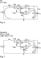
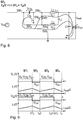
- Fig. 6 to 8 show states 1 (ST 1 ) to 4 (ST 4 ) of the converter 2 in the 3LB mode. Furthermore, fig. 9 shows a time diagram of the voltages V L1 and V L2 across the inductors L 1 and L 2 and of the currents i L1 and i L2 through the inductors L 1 and L 2 .
- state 1 the flying capacitor C fly is charged through the inductors L 1 and L 2 .
- State 2 is a synchronous rectification state.
- state 2 the inductor currents i L1 and i L2 are divided.
- State 3 the flying capacitor C fly is discharged to maintain approximately a constant V in /2 voltage level of V cfly .
- State 4 is a repetition of state 2.
- the 3LB mode can be used under light load conditions, for cases when a high step-down conversion ratio M is required, for example M ⁇ 0.5.
- switches SW 5 and SW 7 are turned on all the times and the inductors L 1 and L 2 are in parallel. This allows the output current I load to be split between the two inductors L 1 and L 2 , reducing the volume requirement and the losses of the inductors L 1 and L 2 .
- the switches SW 1 to SW 7 are switched at half of the input voltage V in, reducing the switching losses.
- the switch operation means 9 further comprise a third switching sequence to perform a third operation mode.
- This operation mode is called first two-phase interleaved buck mode or IB 1 mode.
- the switching sequence of IB 1 mode is as follows: ST 1 ST 2 ST 3 ST 4 SW 1 1 1 1 1 SW 2 1 1 1 1 SW 3 0 0 0 1 SW 4 1 1 1 1 SW 5 1 0 1 1 SW 6 0 1 0 0 SW 7 1 1 1 0 wherein SW 1 to SW 7 denote the mentioned seven switches and ST 1 to ST 4 denote four states of the switching cycle. Furthermore, 0 means OFF and 1 means ON.
- the IB 1 mode can mainly be used for conversion ratios M close to or greater than 0.5.
- Fig. 10 to fig. 12 show state 1 (ST 1 ) to state 4 (ST 4 ) of the converter 2 in the IB 1 mode. Furthermore, fig. 13 shows a time diagram of the voltages V L1 and V L2 across the inductors L 1 and L 2 and the currents i L1 and i L2 through the inductors L 1 and L 2 .
- both inductors L 1 and L 2 are charged with the input voltage V in at the nodes N 3 and N 5 .
- the inductor L 1 continues charging while the inductor L 2 is in synchronous rectification.
- State 3 is a repetition of state 1.
- the inductor L 2 continues charging while the inductor L 1 is in synchronous rectification.
- this operation mode is used for V in ⁇ V in,max /2, where V in,max is the highest allowable input voltage for the converter 2. Since the switches SW 1 , SW 2 and SW 4 remain on in states 1 to 4 the capacitor voltage V cfly is held at the input voltage V in .
- the switch operation means 9 further comprise a fourth switching sequence to perform a fourth operation mode.
- This operation mode is called second two-phase interleaved buck mode or IB 2 mode.
- the switching sequence of the IB 2 mode is as follows: ST 1 ST 2 ST 3 ST 4 SW 1 1 1 1 1 SW 2 1 1 1 1 SW 3 0 1 1 1 SW 4 1 1 1 1 SW 5 0 0 1 0 SW 6 1 1 0 1 SW 7 1 0 0 0
- SW 1 to SW 7 denote the mentioned seven switches
- ST 1 to ST 4 denote four states of a switching cycle.
- 0 means OFF and 1 means ON.
- the IB 2 mode corresponds to the IB 1 mode, whereas for the duty ratio D applies: D ⁇ 0.5.
- Fig. 14 to fig. 16 show state 1 (ST 1 ) to state 4 (ST 4 ) of the converter 2 in the IB 2 mode. Furthermore, fig. 17 shows the voltages V L1 and V L2 across the inductors L 1 and L 2 and the currents i L1 and i L2 through the inductors L 1 and L 2 . In state 2 and state 4 both inductors L 1 and L 2 are discharged. For further details it is referred to the description of the IB 1 mode.
- the switch operation means 9 further comprise a fifth switching sequence to perform a fifth operation mode.
- This operation mode is called single-phase 3-level buck mode or SP3LB mode.
- the switching sequence of the SP3LB mode is as follows: ST 1 ST 2 ST 3 ST 4 SW 1 1 0 0 0 SW 2 0 1 1 1 SW 3 1 1 0 1 SW 4 0 0 1 0 SW 5 0 0 0 0 SW 6 0 0 0 0 SW 7 1 1 1 1 wherein SW 1 to SW 7 denote the mentioned seven switches and ST 1 to ST 4 denote four states of the switching cycle. Furthermore, 0 means OFF and 1 means ON.
- Fig. 18 to fig. 20 show state 1 (ST 1 ) to state 4 (ST 4 ) of the converter 2 in the SP3LB mode.
- fig. 21 shows the voltage V L1 across the inductor L 1 and the current i L1 through the inductor L 1 .
- the SP3LB mode corresponds to the 3LB mode, however, the SP3LB mode uses phase shedding to further increase power processing efficiency at low currents. For further details it is referred to the description of the 3LB mode.
- the switch operation means 9 further comprise a sixth switching sequence to perform a sixth operation mode.
- This operation mode is called single-phase interleaved buck mode or SPIB mode.
- the switching sequence of the SPIB mode is as follows: ST 1 ST 2 SW 1 1 1 SW 2 1 1 SW 3 0 1 SW 4 1 1 SW 5 0 0 SW 6 0 0 SW 7 1 0 wherein SW 1 to SW 7 denote the mentioned seven switches and ST 1 and ST 2 denote two states of the switching cycle. Furthermore, 0 means OFF and 1 means ON.
- Fig. 22 and fig. 23 show state 1 (ST 1 ) and state 2 (ST 2 ) of the converter 2 in the SPIB mode. Furthermore, fig. 24 shows the voltage V L1 across the inductor L 1 and the current i L1 through the inductor L 1 .
- the SPIB mode corresponds to state 1 and state 4 of the IB 1 mode, however, the SPIB mode uses phase shedding to further increase power processing efficiency at low currents. For further details it is referred to the description of the IB 1 mode.
- the mode selection logic 8 determines depending on the input voltage V' in, the required output voltage V ref and the required output current I ref a suitable operation mode. This suitable operation mode is selected from the operation modes mentioned before. For example, the mode selection logic 8 determines a suitable operation mode using a look-up table with predefined voltage thresholds and current thresholds such that the look-up table stores which modes have the highest efficiency for specific operating conditions. The mode selection logic 8 sends a corresponding mode signal S to the switch operation means 9 which contain the mentioned switching sequences for each operation mode. Using the duty ratio D from the voltage compensator 11 and the mode signal S from the mode selection logic 8, the switch operation means 9 operate the switches SW 1 to SW 7 accordingly. In addition, the voltage compensator 11 can be designed with different parameters depending on the operation mode, to achieve an optimized dynamic performance for each mode.
- the converter device 1 is compared to a conventional two-phase interleaved buck converter as known from US 2008/0019158 A1 .
- the switching frequency used for comparison is 800 kHz.
- the energy storage requirements are compared.
- the inductance of the converter 2 can be reduced about 33 %, resulting in smaller inductors L 1 and L 2 .
- the required output capacitor C for the converter 2 can be about 33 % smaller than the conventional two-phase interleaved buck converter to achieve the same transient performance.
- Fig. 25 shows efficiency curves for the conventional two-phase interleaved buck converter (left side) and the converter 2 operating in the HSD mode (right side) for operation point 1.
- the purpose of the HSD mode is to achieve highest efficiency for high step-down ratios.
- the HSD mode improves on the efficiency of the conventional two-phase interleaved buck converter for the entire range of load currents I load .
- the HSD mode enables a loss reduction in the switching losses resulting in the improved efficiency.
- Fig. 26 shows efficiency curves for the conventional two-phase interleaved buck converter (left side) and the 3LB mode and the IB 1 mode of the converter 2 (right side) for operation point 2.
- the highest efficiency mode of the converter 2 depends on load currents I load .
- the 3LB mode has significantly higher efficiency compared to the conventional two-phase interleaved buck converter and compared to the IB 1 mode.
- the IB 1 mode becomes the highest efficiency mode.
- the converter 2 achieves almost equivalent efficiency compared to the conventional two-phase interleaved buck converter.
- the slightly reduced efficiency is caused by higher conduction losses of the IB 1 mode compared to the conventional two-phase interleaved buck converter.
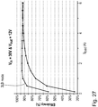
- Fig. 27 shows efficiency curves for the conventional two-phase interleaved buck converter and the 3LB mode of the converter 2 for operation point 3.
- the 3LB mode of the converter 2 has an improved efficiency at light and medium loads for high input voltages. This results from a reduced switch blocking voltage and voltage swing.
- the converter device 1 provides a high power density wide-input DC-DC highly flexible converter topology for a wide range of point of load applications.
- the converter 2 is called 7-switch flying capacitor converter or 7SFC converter.
- the converter 2 requires much smaller inductors L 1 and L 2 compared to a conventional two-phase interleaved buck converter and, at the same time, improves power processing efficiency. These advantages are achieved by reducing the voltage swing across the inductors L 1 and L 2 and the voltage stress of all switches SW 1 to SW 7 to a half of the full input voltage for several operation modes.
- the converter device 1 has in summary the following advantages:
Landscapes
- Engineering & Computer Science (AREA)
- Power Engineering (AREA)
- Dc-Dc Converters (AREA)
Description
- The invention relates to a converter device for converting an input voltage into an output voltage according to the preamble of
claim 1. Furthermore, the invention relates to a method to operate a converter device. - In electronics devices point-of-load (PoL) DC-DC converters are needed to provide regulated DC voltages to various functional blocks in a system. Generally, these functional blocks require different voltage and power levels and, therefore, dedicated PoL converters are used for each block. For these systems, custom designs of the buck converter are used as the PoL converter of choice. The use of custom buck converters allows the designer to maximize efficiency and to minimize volume for each buck converter and to optimize the full system performance. However, custom buck converters increase the system-level design complexity and manufacturing costs and affect reliability.
US 2008/0019158 A1 discloses for example a conventional two-phase interleaved buck converter. - The paper "Digitally Controlled Multi-Phase Buck-Converter with Merged Capacitive Attenuator", Applied Power Electronics Conference and Exposition (APC), 2012, Twenty-Seventh Annual IEEE, published on February 5, 2012, discloses a topology that combines a capacitive divider and a two-phase interleaved buck to reduce the volume of multi-phase step-down converters.
-
US 2008/0159567 A1 discloses an electronic audio amplifier circuit that is operable in two modes. The circuit has a common output stage circuitry for use in both modes and a dual mode power supply unit, ideally a charge pump circuit, for supplying the output stage in the first mode with a lower supply voltage than in the second mode. -
WO 2016/011 380 A1 discloses a two-phase interleaved DC-DC converter that includes a first and a second switched capacitor sub-converter. The converter may operate at a non-resonant or a resonant mode of operation. - It is an object of the present invention to provide a highly flexible converter device that is able to provide a large range of voltages, conversion ratios and power levels with a high power processing efficiency, a low volume and a good dynamic performance.
- This object is achieved by a converter device for converting an input voltage into an output voltage comprising the features of
claim 1. The inventive converter device operates on the principle of transformability, which refers to its ability to choose its mode of operation based on operating conditions. This mode changing characteristic is enabled by seven switches, a flying capacitor and a controller. The controller is in particular a digital controller. The converter in particular comprises exactly seven switches to enable the different operation modes on the one hand and to avoid unnecessary losses on the other hand. Due to the seven switches and the flying capacitor the inventive converter device is in the following also called 7-switch flying capacitor converter device or 7SFC converter device. Correspondingly, the inventive converter is also called 7-switch flying capacitor converter or 7SFC converter. Depending on the operating conditions, the converter device can operate in various operation modes, maximizing efficiency throughout the entire operating range. The operating conditions are characterized by at least one of the input voltage, the output voltage, a required output voltage, an output current, a required output current, a conversion ratio or a duty ratio. For example, at least two of the following operation modes can be provided: high step-down mode, 3-level buck mode, two-phase interleaved buck mode, single-phase 3-level buck mode and single-phase interleaved buck mode. The operation mode with the highest efficiency is selected by the mode selection logic. For example, the mode selection logic comprises a look-up table with predefined voltage thresholds and current thresholds. The converter device is at least one of a step-up converter device or a step-down converter device. - The converter device ensures a high degree of flexibility. The switch operation means provide switching signals to operate the switches dependent on the selected operation mode, namely the operation mode provided by the mode signal of the mode selection logic. The switch operation means comprise in particular a digital pulse width modulator.
- The converter device ensures in the first operation mode a high power processing efficiency for high step-down ratios under medium and heavy load conditions. This operation mode is called high step-down (HSD) mode. This mode provides the highest efficiency for high step-down cases. In steady-state, the voltage across the flying capacitor is equal to half of the input voltage of the converter. That means that all switches can be rated at half of the full input voltage. The benefits of a lower voltage rating for each switch are a reduced volume and reduced switching losses.
- The converter device ensures in the second operation mode a high power processing efficiency under light load conditions for cases when a high step-down conversion is required. This mode is called 3-level buck (3LB) mode. This mode is operated with both inductors in parallel by keeping the fifth switch and the seventh switch on over the full switching cycle. This allows the load current to be split between the two inductors, reducing the volume requirement and losses of the inductors. All switches are switched at half of the input voltage, reducing switching losses.
- The converter device ensures in the third operation mode a high degree of flexibility. This operation mode can be used for conversion ratios close to and greater than 0.5. This mode is called first two-phase interleaved buck (IB1) mode. This mode can be used for a duty ratio D ≥ 0.5.
- The converter device ensures in the fourth operation mode a high degree of flexibility. This operation mode can be used for conversion ratios close to and greater than 0.5. This mode is called second two-phase interleaved buck (IB2) mode. This mode can be used for a duty ratio D ≤ 0.5.
- The converter device ensures in the fifth operation mode a high degree of flexibility. This operation mode enables to perform phase shedding to further increase power processing efficiency at low currents. This operation mode is called single-phase 3-level buck (SP3LB) mode.
- The converter device ensures in the sixth operation mode a high degree of flexibility. This operation mode enables to perform phase shedding to further increase power processing efficiency at low currents. This operation mode is called single-phase interleaved buck (SPIB) mode.
- In case the converter device is operated as step-down converter device, there applies to a conversion ratio M = Vout/Vin: 1/24 ≤ M ≤ 1, preferably 1/48 ≤ M ≤ 1, preferably 1/80 ≤ M ≤ 1.
- Furthermore, in case the converter device is operated as step-up converter device, there applies to the conversion ratio M: 1 ≤ M ≤ 24, preferably 1 ≤ M ≤ 48, preferably 1 ≤ M ≤ 80.
- The converter device is operated at a switching frequency fs. For example, there applies to the switching frequency: 200 kHz ≤ fS ≤ 1600 kHz, preferably 400 kHz ≤ fS ≤ 1400 kHz, preferably 600 kHz ≤ fS ≤ 1200 kHz.
- Furthermore, there applies for example to a load current Iload: 0,1 A ≤ Iload ≤ 10 A, preferably 0,5 A ≤ Iload ≤ 8 A and preferably 1 A ≤ Iload ≤ 6 A.
- A power processing efficiency of the converter device is defined as the ratio of the output power and the input power. The power processing efficiency depends on the conversion ratio M, the switching frequency fs and/or the load current Iload. The power processing efficiency is at least 75 %, preferably at least 80 %, preferably at least 85 %, and preferably at least 90 % for the entire range of operating conditions. The converter device maintains a high and almost flat efficiency curve for the entire range of operating conditions.
- The converter device ensures a high degree of flexibility. The arrangement of the seven switches allows the inventive two-phase DC-DC converter to perform various different operation modes. Furthermore, the converter device enables a reduction of voltage stress across the reactive components to half of the input voltage in case of a step-down converter device or to half of the output voltage in case of a step-up converter device. The second input voltage terminal and the second output voltage terminal are in particular connected to the reference node. The reference node is in particular connected to ground.
- The converter device ensures a high power processing efficiency due to a reduction in switching losses and voltage stress. The voltage across the flying capacitor is equal to half of the input voltage in case of a step-down converter device or half of the output voltage in case of a step-up converter device for certain operation modes. This enables a reduced voltage stress of the switches and the reactive components and a reduced volume of the reactive components. Furthermore, the switching losses of the switches are reduced.
- Both inductors can be operated in parallel. This allows the load current to be split between the two inductors, reducing the volume requirement and losses of the inductors.
- A converter device according to
claim 2 ensures a high degree of flexibility. In case of a step-down converter device the output capacitor enables to adapt the output voltage ripple and the deviation of the output voltage to a desired value. The capacitor is in particular connected to the reference node. - A converter device according to
claim 3 enables to provide a regulated output voltage. The voltage controller provides the switch operation means with a duty ratio to operate the switches dependent on said duty ratio. The output voltage is measured by a voltage sensor and preferably transferred into the digital domain by a corresponding analogue-to-digital converter. A digital voltage compensator is provided with an error signal which is the difference of a desired digital output voltage and the measured digital output voltage. The output signal of the digital voltage compensator is the duty ratio D. The duty ratio D is the ratio of a pulse duration T and a switching period Ts. There applies to the duty ratio: 0 ≤ D ≤ 1, in particular 0 < D < 1. - A converter device according to
claim 4 ensures a high degree of flexibility and a high power processing efficiency. Based on signals, preferably digital signals of the input voltage, the output voltage and the output current the mode selection logic determines a suitable operation mode. For example, the mode selection logic uses a look-up table to provide a mode signal to the switch operation means which characterizes a suitable operation mode. In addition, the voltage compensator can be designed with different parameters, depending on the operation mode to achieve an optimized dynamic performance for each operation mode. - Furthermore, it is an object of the present invention to provide a highly flexible method to operate a converter device that is able to provide a large range of voltages, conversion ratios and power levels with a high power processing efficiency, a low volume, and a good dynamic performance.
- This object is achieved by a method to operate a converter device comprising the steps of
claim 5. The advantages of the method according to the invention correspond to the advantages already described of the converter device according to the invention. - Further features, advantages and details of the invention will be apparent from the following description of an embodiment which refers to the accompanying drawings.
- Fig. 1
- shows a schematic diagram of a converter device with a converter and a digital controller,
- Fig. 2
- shows a first state of the converter in a high step-down mode,
- Fig. 3
- shows a second and a fourth state of the converter in the high step-down mode,
- Fig. 4
- shows a third state of the converter in the high step-down mode,
- Fig. 5
- shows a time diagram of voltages and currents of the converter in the high step-down mode,
- Fig. 6
- shows a first state of the converter in a 3-level buck mode,
- Fig. 7
- shows a second and a fourth state of the converter in the 3-level buck mode,
- Fig. 8
- shows a third state of the converter in the 3-level buck mode,
- Fig. 9
- shows a time diagram of voltages and currents of the converter in the 3-level buck mode,
- Fig. 10
- shows a first and a third state of the converter in a first two-phase interleaved buck mode,
- Fig. 11
- shows a second state of the converter in the first two-phase interleaved buck mode,
- Fig. 12
- shows a fourth state of the converter in the first two-phase interleaved buck mode,
- Fig. 13
- shows a time diagram of voltages and currents of the converter in the first two-phase interleaved buck mode,
- Fig. 14
- shows a first state of the converter in a second two-phase interleaved buck mode,
- Fig. 15
- shows a second state and a fourth state of the converter in the second two-phase interleaved buck mode,
- Fig. 16
- shows a third state of the converter in the second two-phase interleaved buck mode,
- Fig. 17
- shows a time diagram of voltages and currents of the converter in the second two-phase interleaved buck mode,
- Fig. 18
- shows a first state of the converter in a single-phase 3-level buck mode,
- Fig. 19
- shows a second state and a fourth state of the converter in the single-phase 3-level buck mode,
- Fig. 20
- shows a third state of the converter in the single-phase 3-level buck mode,
- Fig. 21
- shows a time diagram of a voltage and a current of the converter in the single-phase 3-level buck mode,
- Fig. 22
- shows a first state of the converter in a single-phase interleaved buck mode,
- Fig. 23
- shows a second state of the converter in the single-phase interleaved buck mode,
- Fig. 24
- shows a time diagram of a voltage and a current of the converter in the single-phase interleaved buck mode,
- Fig. 25
- shows efficiency curves of a conventional two-phase interleaved buck converter and the inventive converter for a first operating point,
- Fig. 26
- shows efficiency curves of a conventional two-phase interleaved buck converter and the inventive converter for a second operating point and
- Fig. 27
- shows efficiency curves of a conventional two-phase interleaved buck converter and the inventive converter for a third operating point.
-
Fig. 1 shows aconverter device 1 for converting an input voltage Vin into an output voltage Vout. Theconverter device 1 comprises aconverter 2 and adigital controller 3 to operate theconverter 2. Theconverter device 1 is for example used to convert the DC-DC input voltage Vin into a smaller DC-DC output voltage Vout. A step-down ratio or a conversion ratio M is defined as follows: M = Vout/Vin. - The
converter 2 comprises a first input voltage terminal in1 and second input voltage terminal in2 to apply the input voltage Vin. Furthermore, theconverter 2 comprises a first output voltage terminal out1 and a second output voltage terminal out2 to provide the output voltage Vout and an output current or load current Iload to a load R. Theconverter 2 further comprises for reactive components, namely a flying capacitor Cfly, a capacitor C, a first inductor L1 and a second inductor L2. - In case that the
converter 2 is operated as step-downconverter 2, the first input voltage terminal in1 is connected via a first switch SW1 to a first node N1. The first node N1 is connected via the flying capacitor Cfly to a second node N2. The second node N2 is connected via a second switch SW2 to a reference node N0. The second node N2 further is connected via a third switch SW3 to a third node N3. The third node N3 is connected via the inductor L1 with the first output voltage terminal out1. The first node N1 is further connected via a fourth switch SW4 to a fourth node N4. Furthermore, the fourth node N4 is connected via a fifth switch SW5 to a fifth node N5. The fifth node N5 is further connected via the second inductor L2 to the first output terminal out1. The fifth node N5 is connected via a sixth switch SW6 to the reference node N0. The third node N3 is further connected via a seventh switch SW7 to the fourth node N4. The output capacitor C is arranged in parallel to the first output voltage terminal out1 and the second output voltage terminal out2. This means that the first output voltage terminal out1 is connected via the output capacitor C with the second output voltage terminal out2. The reference node N0, the second input voltage terminal in2 and the second output voltage terminal out2 are connected to ground. - In case that the
converter 2 is operated as step-upconverter 2, the input voltage terminals in1, in2 and the output voltage terminals out1, out2 are exchanged. In this case the capacitor C is called input capacitor C. - The input voltage Vin is measured by means of a
first voltage sensor 4 and provided to an analog-to-digital converter 5. The analog-to-digital converter 5 transfers the input voltage Vin into the digital domain and provides a digital input voltage signal V'in to thedigital controller 3. Correspondingly, the output voltage Vout is measured by asecond voltage sensor 6 and provided to a further analog-to-digital converter 7. The analog-to-digital converter 7 transfers the output voltage Vout into the digital domain and provides a digital output voltage signal V'out to thedigital controller 3. - The
digital controller 3 comprises a mode selection logic 8, switch operation means 9 and adigital voltage controller 10. The mode selection logic has three signal inputs to receive the input voltage V'in, a required output voltage Vref and a required output current Iref. The mode selection logic 8 generates a mode signal S to select a suitable operation mode from a group of a different operation modes depending on the input voltage V'in, the required output voltage Vref and/or the required output current Iref. For example, the mode selection logic 8 comprises a look-up table which generates the mode signal S dependent on the desired conversion ratio M and the load conditions which are characterized by the required output current Iref. The switch operation means 9 are connected with the mode selection logic 8 to receive the mode signal S and to operate the switches SW1 to SW7 dependent on the selected operation mode. - The
digital voltage controller 10 comprises avoltage compensator 11 which receives an output voltage error signal e = Vref - V'out. Thevoltage compensator 11 calculates a duty ratio D. The switch operation means 9 are connected to thedigital voltage controller 10 to receive the duty ratio D and to operate the switches SW1 to SW7 dependent on the duty ratio D. The duty ratio D is the ratio between a desired pulse duration and a switching period TS. - The switch operation means 9 are connected to the switches SW1 to SW7 and generate for each switch SW1 to SW7 a corresponding switching signal G1 to G7. The switches SW1 to SW7 are switched on or switched off depending on the signal level of the corresponding switching signal G1 to G7. The switches SW1 to SW7 are for example MOSFETs.
- The switch operation means 9 comprise a first switching sequence to perform a first operation mode. This operation mode is called high step-down mode or HSD mode. The switching sequence of the HSD mode is as follows:
ST1 ST2 ST3 ST4 SW1 1 0 0 0 SW 20 1 1 1 SW 31 1 1 1 SW 40 0 1 0 SW 50 1 1 1 SW 61 1 0 1 SW 71 1 0 1 -
Fig. 2 to fig. 4 show theconverter 2 in the states 1 (ST1) to 4 (ST4) of the switching cycle. Furthermore,fig. 5 shows a time diagram of the voltages VL1 and VL2 across the inductors L1 and L2 and of the currents iL1 and iL2 through the inductors L1 and L2. t denotes the time and TS the switching period of the switching cycle. The duration of thestates 1 to 4 depends on the duty ratio D. - The HSD mode has a high power processing efficiency for high step-down ratios M under medium and heavy load conditions. In steady-state, the voltage VCfly across the flying capacitor Cfly is equal to half of the input voltage Vin. The switching sequence consists of the four states ST1 to ST4, where in
state 1 the flying capacitor Cfly and the inductor L1 are charged with energy.State 2 is a synchronous rectification state. In thisstate 2 the inductor currents iL1 and iL2 are divided. Due to this current distribution the power losses are reduced. Duringstate 3 the flying capacitor Cfly is discharged and the inductor L2 is charged.State 4 is a repetition ofstate 2. - The flying capacitor voltage Vcfly is maintained at Vin/2 by the two inductors L1 and L2 and the conversion ratio is M (D) = Vout/Vin = D/2. In the HSD mode the variations of the switching node voltages VL1 and VL2 are reduced by a half compared to a conventional two-phase interleaved buck converter, allowing for a significant reduction of the inductance value of the inductors L1 and L2. Since the capacitors Cfly and C have up to three orders of magnitude smaller volume for the same amount of stored energy than the inductors L1 and L2 the overall volume of reactive components of the
converter 2 is reduced compared to a conventional two-phase interleaved buck converter. In the HSD mode all switches SW1 to SW7 are blocking only a half of the input voltage Vin. This means that, if the same silicon area is used for the two implementations, both switching and conduction losses for semiconductor components of this topology could potentially be smaller than that of a conventional two-phase interleaved buck converter. - The switch operation means 9 further comprise a second switching sequence to perform a second operation mode. This second operation mode is called 3-level buck mode or 3LB mode. The switching sequence of the 3LB mode is as follows:
ST1 ST2 ST3 ST4 SW1 1 0 0 0 SW 20 1 1 1 SW 31 1 0 1 SW 40 0 1 0 SW 51 1 1 1 SW 60 1 0 1 SW 71 1 1 1 -
Fig. 6 to 8 show states 1 (ST1) to 4 (ST4) of theconverter 2 in the 3LB mode. Furthermore,fig. 9 shows a time diagram of the voltages VL1 and VL2 across the inductors L1 and L2 and of the currents iL1 and iL2 through the inductors L1 and L2. - In
state 1 the flying capacitor Cfly is charged through the inductors L1 and L2. State 2 is a synchronous rectification state. Instate 2 the inductor currents iL1 and iL2 are divided. InState 3 the flying capacitor Cfly is discharged to maintain approximately a constant Vin/2 voltage level of Vcfly. State 4 is a repetition ofstate 2. - The 3LB mode can be used under light load conditions, for cases when a high step-down conversion ratio M is required, for example M < 0.5. In the 3LB mode switches SW5 and SW7 are turned on all the times and the inductors L1 and L2 are in parallel. This allows the output current Iload to be split between the two inductors L1 and L2, reducing the volume requirement and the losses of the inductors L1 and L2. The 3LB mode operates with a range of the duty ratio D of 0 < D < 0.5 and a conversion ratio of M (D) = D. The switches SW1 to SW7 are switched at half of the input voltage Vin, reducing the switching losses.
- The switch operation means 9 further comprise a third switching sequence to perform a third operation mode. This operation mode is called first two-phase interleaved buck mode or IB1 mode. The switching sequence of IB1 mode is as follows:
ST1 ST2 ST3 ST4 SW1 1 1 1 1 SW 21 1 1 1 SW 30 0 0 1 SW 41 1 1 1 SW 51 0 1 1 SW 60 1 0 0 SW 71 1 1 0 -
Fig. 10 to fig. 12 show state 1 (ST1) to state 4 (ST4) of theconverter 2 in the IB1 mode. Furthermore,fig. 13 shows a time diagram of the voltages VL1 and VL2 across the inductors L1 and L2 and the currents iL1 and iL2 through the inductors L1 and L2. - In
state 1 both inductors L1 and L2 are charged with the input voltage Vin at the nodes N3 and N5. Instate 2 the inductor L1 continues charging while the inductor L2 is in synchronous rectification.State 3 is a repetition ofstate 1. Instate 4 the inductor L2 continues charging while the inductor L1 is in synchronous rectification. To keep all of the switch ratings at Vin,max/2 this operation mode is used for Vin < Vin,max/2, where Vin,max is the highest allowable input voltage for theconverter 2. Since the switches SW1, SW2 and SW4 remain on instates 1 to 4 the capacitor voltage Vcfly is held at the input voltage Vin. - The switch operation means 9 further comprise a fourth switching sequence to perform a fourth operation mode. This operation mode is called second two-phase interleaved buck mode or IB2 mode. The switching sequence of the IB2 mode is as follows:
ST1 ST2 ST3 ST4 SW1 1 1 1 1 SW 21 1 1 1 SW 30 1 1 1 SW 41 1 1 1 SW 50 0 1 0 SW 61 1 0 1 SW 71 0 0 0 -
Fig. 14 to fig. 16 show state 1 (ST1) to state 4 (ST4) of theconverter 2 in the IB2 mode. Furthermore,fig. 17 shows the voltages VL1 and VL2 across the inductors L1 and L2 and the currents iL1 and iL2 through the inductors L1 and L2. Instate 2 andstate 4 both inductors L1 and L2 are discharged. For further details it is referred to the description of the IB1 mode. - The switch operation means 9 further comprise a fifth switching sequence to perform a fifth operation mode. This operation mode is called single-phase 3-level buck mode or SP3LB mode. The switching sequence of the SP3LB mode is as follows:
ST1 ST2 ST3 ST4 SW1 1 0 0 0 SW 20 1 1 1 SW 31 1 0 1 SW 40 0 1 0 SW 50 0 0 0 SW 60 0 0 0 SW 71 1 1 1 -
Fig. 18 to fig. 20 show state 1 (ST1) to state 4 (ST4) of theconverter 2 in the SP3LB mode. Furthermore,fig. 21 shows the voltage VL1 across the inductor L1 and the current iL1 through the inductor L1. In general the SP3LB mode corresponds to the 3LB mode, however, the SP3LB mode uses phase shedding to further increase power processing efficiency at low currents. For further details it is referred to the description of the 3LB mode. - The switch operation means 9 further comprise a sixth switching sequence to perform a sixth operation mode. This operation mode is called single-phase interleaved buck mode or SPIB mode. The switching sequence of the SPIB mode is as follows:
ST1 ST2 SW1 1 1 SW 21 1 SW 30 1 SW 41 1 SW 50 0 SW 60 0 SW 71 0 -
Fig. 22 and fig. 23 show state 1 (ST1) and state 2 (ST2) of theconverter 2 in the SPIB mode. Furthermore,fig. 24 shows the voltage VL1 across the inductor L1 and the current iL1 through the inductor L1. In general the SPIB mode corresponds tostate 1 andstate 4 of the IB1 mode, however, the SPIB mode uses phase shedding to further increase power processing efficiency at low currents. For further details it is referred to the description of the IB1 mode. - The mode selection logic 8 determines depending on the input voltage V'in, the required output voltage Vref and the required output current Iref a suitable operation mode. This suitable operation mode is selected from the operation modes mentioned before. For example, the mode selection logic 8 determines a suitable operation mode using a look-up table with predefined voltage thresholds and current thresholds such that the look-up table stores which modes have the highest efficiency for specific operating conditions. The mode selection logic 8 sends a corresponding mode signal S to the switch operation means 9 which contain the mentioned switching sequences for each operation mode. Using the duty ratio D from the
voltage compensator 11 and the mode signal S from the mode selection logic 8, the switch operation means 9 operate the switches SW1 to SW7 accordingly. In addition, thevoltage compensator 11 can be designed with different parameters depending on the operation mode, to achieve an optimized dynamic performance for each mode. - The
converter device 1 is compared to a conventional two-phase interleaved buck converter as known fromUS 2008/0019158 A1 . The switching frequency used for comparison is 800 kHz. - To compare the volume of the reactive components of the
converter 2 to a conventional two-phase interleaved buck converter the energy storage requirements are compared. To achieve the same current ripple in the inductors, the inductance of theconverter 2 can be reduced about 33 %, resulting in smaller inductors L1 and L2. Furthermore, to achieve a desired output voltage deviation in response to a load transient, the required output capacitor C for theconverter 2 can be about 33 % smaller than the conventional two-phase interleaved buck converter to achieve the same transient performance. - To show the efficiency improvements of the
converter device 1 over the conventional two-phase interleaved buck converter, the following three operation points are compared between the mentioned converters: - Operation point 1: Vin = 12V and Vout = 1V,
- Operation point 2: Vin = 12V and Vout = 5V,
- Operation point 3: Vin = 36V and Vout = 12V.
-
Fig. 25 shows efficiency curves for the conventional two-phase interleaved buck converter (left side) and theconverter 2 operating in the HSD mode (right side) foroperation point 1. The purpose of the HSD mode is to achieve highest efficiency for high step-down ratios. Atoperation point 1 the HSD mode improves on the efficiency of the conventional two-phase interleaved buck converter for the entire range of load currents Iload. The HSD mode enables a loss reduction in the switching losses resulting in the improved efficiency. -
Fig. 26 shows efficiency curves for the conventional two-phase interleaved buck converter (left side) and the 3LB mode and the IB1 mode of the converter 2 (right side) foroperation point 2. Foroperation point 2 the highest efficiency mode of theconverter 2 depends on load currents Iload. At the low end of load currents, the 3LB mode has significantly higher efficiency compared to the conventional two-phase interleaved buck converter and compared to the IB1 mode. As the load current is increased the IB1 mode becomes the highest efficiency mode. For this segment of load currents theconverter 2 achieves almost equivalent efficiency compared to the conventional two-phase interleaved buck converter. The slightly reduced efficiency is caused by higher conduction losses of the IB1 mode compared to the conventional two-phase interleaved buck converter. -
Fig. 27 shows efficiency curves for the conventional two-phase interleaved buck converter and the 3LB mode of theconverter 2 foroperation point 3. The 3LB mode of theconverter 2 has an improved efficiency at light and medium loads for high input voltages. This results from a reduced switch blocking voltage and voltage swing. - By properly selecting operation modes of the
converter 2, efficiency improvements are achievable over the full operating range. - The
converter device 1 provides a high power density wide-input DC-DC highly flexible converter topology for a wide range of point of load applications. Theconverter 2 is called 7-switch flying capacitor converter or 7SFC converter. Theconverter 2 requires much smaller inductors L1 and L2 compared to a conventional two-phase interleaved buck converter and, at the same time, improves power processing efficiency. These advantages are achieved by reducing the voltage swing across the inductors L1 and L2 and the voltage stress of all switches SW1 to SW7 to a half of the full input voltage for several operation modes. Theconverter device 1 has in summary the following advantages: - multi-mode switch operation, in particular facilitated by the
digital controller 3, - operating point based efficiency optimization,
- significantly improved high step-down ratio efficiency over a conventional two-phase interleaved buck converter by significantly reducing switching losses,
- reduced inductor volume requirement,
- reduced output capacitor requirement,
- a reduced silicon area for the switches SW1 to SW7 compared to a conventional two-phase interleaved buck converter.
Claims (5)
- Converter device for converting an input voltage into an output voltage, comprising- a converter (2) comprising-- a first input voltage terminal (in1) and a second input voltage terminal (in2) to apply the input voltage (Vin),-- a first output voltage terminal (out1) and a second output voltage terminal (out2) to provide the output voltage (Vout) to a load (R),-- reactive components (Cfly, C, L1, L2), which comprise a flying capacitor (Cfly),-- seven switches SW1 to SW7 to perform at least two different operation modes,- a controller (3) to operate the converter (2), which comprisescharacterized in that-- a mode selection logic (8) to select one of the operation modes depending on desired operating conditions,-- switch operation means (9), which are connected with the mode selection logic (8) to receive a mode signal (S) and to operate the switches SW1 to SW7 dependent on the selected operation mode,- a first switch SW1 is connected to one of the first voltage terminals (in1) and a first node (N1),- a second switch SW2 is connected to a second node (N2) and a reference node (N0),- a third switch SW3 is connected to the second node (N2) and a third node (N3),- a fourth switch SW4 is connected to the first node (N1) and a fourth node (N4),- a fifth switch SW5 is connected to the fourth node (N4) and a fifth node (N5),- a sixth switch SW6 is connected to the fifth node (N5) and the reference node (N0), and- a seventh switch SW7 is connected to the third node (N3) and the fourth node (N4),- the flying capacitor (Cfly) is connected to the first node (N1) and the second node (N2),- the reactive components (Cfly, C, L1, L2) comprise a first inductor (L1) which is connected to the third node (N3) and one of the first voltage terminals (out1) and a second inductor (L2) which is connected to the fifth node (N5) and said one first voltage terminal (out1),- the switch operation means (9) comprise at least two ofa first switching sequence to perform a first operation mode as follows:
ST1 ST2 ST3 ST4 SW1 1 0 0 0 SW2 0 1 1 1 SW3 1 1 1 1 SW4 0 0 1 0 SW5 0 1 1 1 SW6 1 1 0 1 SW7 1 1 0 1 SW1 to SW7 denote the seven switches,ST1 to ST4 denote four states of a switching cycle,0 means OFF and 1 means ON,a second switching sequence to perform a second operation mode as follows:ST1 ST2 ST3 ST4 SW1 1 0 0 0 SW2 0 1 1 1 SW3 1 1 0 1 SW4 0 0 1 0 SW5 1 1 1 1 SW6 0 1 0 1 SW7 1 1 1 1 SW1 to SW7 denote the seven switches,ST1 to ST4 denote four states of a switching cycle,0 means OFF and 1 means ON,a third switching sequence to perform a third operation mode as follows:ST1 ST2 ST3 ST4 SW1 1 1 1 1 SW2 1 1 1 1 SW3 0 0 0 1 SW4 1 1 1 1 SW5 1 0 1 1 SW6 0 1 0 0 SW7 1 1 1 0 SW1 to SW7 denote the seven switches,ST1 to ST4 denote four states of a switching cycle,0 means OFF and 1 means ON,a fourth switching sequence to perform a fourth operation mode as follows:ST1 ST2 ST3 ST4 SW1 1 1 1 1 SW2 1 1 1 1 SW3 0 1 1 1 SW4 1 1 1 1 SW5 0 0 1 0 SW6 1 1 0 1 SW7 1 0 0 0 SW1 to SW7 denote the seven switches,ST1 to ST4 denote four states of a switching cycle,0 means OFF and 1 means ON,a fifth switching sequence to perform a fifth operation mode as follows:ST1 ST2 ST3 ST4 SW1 1 0 0 0 SW2 0 1 1 1 SW3 1 1 0 1 SW4 0 0 1 0 SW5 0 0 0 0 SW6 0 0 0 0 SW7 1 1 1 1 SW1 to SW7 denote the seven switches,ST1 to ST4 denote four states of a switching cycle,0 means OFF and 1 means ON,a sixth switching sequence to perform a sixth operation mode as follows:ST1 ST2 SW1 1 1 SW2 1 1 SW3 0 1 SW4 1 1 SW5 0 0 SW6 0 0 SW7 1 0 SW1 to SW7 denote the seven switches,ST1 and ST2 denote two states of a switching cycle,0 means OFF and 1 means ON. - Converter device according to claim 1 , characterized in that the reactive components (Cfly, C, L1, L2) comprise a capacitor (C) which is arranged in parallel to one of the first voltage terminals (out1) and the associated second voltage terminal (out2).
- Converter device according to at least one of claims 1 or 2, characterized in that
the digital controller (3) comprises a voltage controller (10) which is connected to the switch operation means (9) to provide a duty ratio (D) and to operate the switches SW1 to SW7 dependent on the duty ratio (D). - Converter device according to at least one of claims 1 to 3, characterized in that
the mode selection logic (8) comprises at least three signal inputs to receive the input voltage (V'in), the output voltage (Vref) and the output current (Iref). - Method to operate a converter device, comprising the following steps:- providing a converter device (1) according to at least one of claims 1 to 4,- selecting one of the at least two operation modes by means of the mode selection logic (8) depending on desired operating conditions, and- operating the switches SW1 to SW7 of the converter (2) to perform the selected operation mode.
Priority Applications (10)
| Application Number | Priority Date | Filing Date | Title |
|---|---|---|---|
| EP16161038.1A EP3220525B1 (en) | 2016-03-18 | 2016-03-18 | Converter device and method to operate said converter device |
| KR1020187020697A KR102159570B1 (en) | 2016-03-18 | 2017-03-15 | Converter device and method of operating it |
| HK18116672.1A HK1257439B (en) | 2016-03-18 | 2017-03-15 | Converter device and method to operate said converter device |
| US16/085,708 US10720836B2 (en) | 2016-03-18 | 2017-03-15 | Converter device and method to operate said converter device |
| CN201780016335.4A CN108781038B (en) | 2016-03-18 | 2017-03-15 | Converter device and method for operating the same |
| PCT/EP2017/056124 WO2017158022A1 (en) | 2016-03-18 | 2017-03-15 | Converter device and method to operate said converter device |
| CA3018104A CA3018104C (en) | 2016-03-18 | 2017-03-15 | Converter device and method to operate said converter device |
| JP2018527195A JP6694956B2 (en) | 2016-03-18 | 2017-03-15 | Converter device and operating method thereof |
| RU2018119973A RU2704247C9 (en) | 2016-03-18 | 2017-03-15 | Converter device and method of controlling said converter device |
| TW106108940A TWI636649B (en) | 2016-03-18 | 2017-03-17 | Converter device and method to operate said converter device |
Applications Claiming Priority (1)
| Application Number | Priority Date | Filing Date | Title |
|---|---|---|---|
| EP16161038.1A EP3220525B1 (en) | 2016-03-18 | 2016-03-18 | Converter device and method to operate said converter device |
Publications (2)
| Publication Number | Publication Date |
|---|---|
| EP3220525A1 EP3220525A1 (en) | 2017-09-20 |
| EP3220525B1 true EP3220525B1 (en) | 2018-10-24 |
Family
ID=55586201
Family Applications (1)
| Application Number | Title | Priority Date | Filing Date |
|---|---|---|---|
| EP16161038.1A Active EP3220525B1 (en) | 2016-03-18 | 2016-03-18 | Converter device and method to operate said converter device |
Country Status (9)
| Country | Link |
|---|---|
| US (1) | US10720836B2 (en) |
| EP (1) | EP3220525B1 (en) |
| JP (1) | JP6694956B2 (en) |
| KR (1) | KR102159570B1 (en) |
| CN (1) | CN108781038B (en) |
| CA (1) | CA3018104C (en) |
| RU (1) | RU2704247C9 (en) |
| TW (1) | TWI636649B (en) |
| WO (1) | WO2017158022A1 (en) |
Families Citing this family (3)
| Publication number | Priority date | Publication date | Assignee | Title |
|---|---|---|---|---|
| CN111509980B (en) | 2019-01-31 | 2021-04-13 | 台达电子工业股份有限公司 | power converter |
| CN111245236B (en) * | 2020-03-16 | 2020-12-22 | 深圳市诚芯微科技有限公司 | A Buck DC-DC Converter Topology |
| CN115378254B (en) * | 2022-05-19 | 2025-07-11 | 捷蒽迪电子科技(上海)有限公司 | A non-isolated step-down switching converter |
Family Cites Families (8)
| Publication number | Priority date | Publication date | Assignee | Title |
|---|---|---|---|---|
| US7449867B2 (en) * | 2005-07-26 | 2008-11-11 | International Rectifier Corporation | Multi-phase buck converter with a plurality of coupled inductors |
| GB2444988B (en) * | 2006-12-22 | 2011-07-20 | Wolfson Microelectronics Plc | Audio amplifier circuit and electronic apparatus including the same |
| US8274264B2 (en) * | 2010-02-19 | 2012-09-25 | Exar Corporation | Digital control method for improving heavy-to-light (step down) load transient response of switch mode power supplies |
| RU2462807C1 (en) | 2011-07-07 | 2012-09-27 | Государственное образовательное учреждение высшего профессионального образования "Поволжский государственный университет телекоммуникаций и информатики" (ГОУВПО ПГУТИ) | Constant voltage converter |
| TWI497254B (en) | 2012-07-19 | 2015-08-21 | Alpha Imaging Technology Corp | Switch circuit and charge pump using the same thereof |
| GB2510395A (en) | 2013-02-01 | 2014-08-06 | Nujira Ltd | Voltage supply stage for an envelope tracking modulated power supply |
| US10615692B2 (en) * | 2014-04-25 | 2020-04-07 | Texas Instruments Incorporated | Series capacitor buck converter having circuitry for precharging the series capacitor |
| US20170201177A1 (en) * | 2014-07-17 | 2017-07-13 | The Trustees Of Dartmouth College | System and method for two-phase interleaved dc-dc converters |
-
2016
- 2016-03-18 EP EP16161038.1A patent/EP3220525B1/en active Active
-
2017
- 2017-03-15 JP JP2018527195A patent/JP6694956B2/en active Active
- 2017-03-15 CN CN201780016335.4A patent/CN108781038B/en active Active
- 2017-03-15 CA CA3018104A patent/CA3018104C/en active Active
- 2017-03-15 WO PCT/EP2017/056124 patent/WO2017158022A1/en not_active Ceased
- 2017-03-15 KR KR1020187020697A patent/KR102159570B1/en active Active
- 2017-03-15 US US16/085,708 patent/US10720836B2/en active Active
- 2017-03-15 RU RU2018119973A patent/RU2704247C9/en active
- 2017-03-17 TW TW106108940A patent/TWI636649B/en active
Non-Patent Citations (1)
| Title |
|---|
| None * |
Also Published As
| Publication number | Publication date |
|---|---|
| RU2704247C9 (en) | 2020-02-11 |
| RU2704247C1 (en) | 2019-10-25 |
| CA3018104A1 (en) | 2017-09-21 |
| JP2019508997A (en) | 2019-03-28 |
| US20190097536A1 (en) | 2019-03-28 |
| TWI636649B (en) | 2018-09-21 |
| KR20180124017A (en) | 2018-11-20 |
| TW201735515A (en) | 2017-10-01 |
| JP6694956B2 (en) | 2020-05-20 |
| CA3018104C (en) | 2022-10-04 |
| CN108781038B (en) | 2021-02-05 |
| EP3220525A1 (en) | 2017-09-20 |
| HK1257439A1 (en) | 2019-10-18 |
| WO2017158022A1 (en) | 2017-09-21 |
| KR102159570B1 (en) | 2020-09-24 |
| US10720836B2 (en) | 2020-07-21 |
| CN108781038A (en) | 2018-11-09 |
Similar Documents
| Publication | Publication Date | Title |
|---|---|---|
| Meraj et al. | Interleaved multilevel boost converter with minimal voltage multiplier components for high-voltage step-up applications | |
| US9276470B2 (en) | Multiphase switching converters operating over wide load ranges | |
| US6979980B1 (en) | Soft switching interleaved power converter | |
| EP2994986B1 (en) | Buck-boost switching converter with buck-boost transition switching control and corresponding method | |
| EP2270964B1 (en) | Method of controlling a power factor correction stage, a power factor correction stage and a controller therefor | |
| Hata et al. | Always-dual-path hybrid DC-DC converter achieving high efficiency at around 2: 1 step-down ratio | |
| EP3399634B1 (en) | Isolated bidirectional dc-dc converter | |
| WO2016038601A1 (en) | A voltage regulator module using a load-side auxiliary gyrator circuit | |
| KR20090044137A (en) | Transformerless Boost Converter | |
| Chen et al. | A new bidirectional DC-DC converter with a high step-up/down conversion ratio for renewable energy applications | |
| US10720836B2 (en) | Converter device and method to operate said converter device | |
| US8331110B2 (en) | Switching capacitor—PWM power converter | |
| JP2019097273A (en) | Power conversion device | |
| KR101857947B1 (en) | Interleaved type dc-dc converting apparatus | |
| KR102036753B1 (en) | Ac-dc converting apparatus for reducing a current ripple | |
| Huang et al. | Single-inductor dual-output DC-DC converters with high light-load efficiency and minimized cross-regulation for portable devices | |
| WO2019213673A1 (en) | Buck matrix-type rectifier with boost switch, and operation thereof during one-phase loss | |
| Martínez García et al. | On single-input dual-output (SIDO) DC/DC multi-port converters for DC microgrid applications | |
| US20250300559A1 (en) | Systems and methods for traversing non-linearity of a mode boundary of a power converter | |
| Chen et al. | An All-GaN 90.6% Peak Efficiency Switch-Rationalized 48V-to-Point-of-Load Hybrid Power Converter with Digitally Auto-locked V CF Control Achieving 1,158 A/inch 3 Current Density | |
| Pattnaik et al. | An improved multiphase converter for new generation microprocessr | |
| Da Fonseca et al. | Analysis and Design of DC-DC Buck-Boost Converter with Continuous Input Current | |
| Kohama et al. | Design guidelines for low-ripple paralleled converter system | |
| KR101356385B1 (en) | Power converting apparatus and control method for power converter | |
| KR101798879B1 (en) | Two-stage differential buck converter and control method thereof |
Legal Events
| Date | Code | Title | Description |
|---|---|---|---|
| PUAI | Public reference made under article 153(3) epc to a published international application that has entered the european phase |
Free format text: ORIGINAL CODE: 0009012 |
|
| STAA | Information on the status of an ep patent application or granted ep patent |
Free format text: STATUS: REQUEST FOR EXAMINATION WAS MADE |
|
| 17P | Request for examination filed |
Effective date: 20170804 |
|
| AK | Designated contracting states |
Kind code of ref document: A1 Designated state(s): AL AT BE BG CH CY CZ DE DK EE ES FI FR GB GR HR HU IE IS IT LI LT LU LV MC MK MT NL NO PL PT RO RS SE SI SK SM TR |
|
| AX | Request for extension of the european patent |
Extension state: BA ME |
|
| STAA | Information on the status of an ep patent application or granted ep patent |
Free format text: STATUS: EXAMINATION IS IN PROGRESS |
|
| 17Q | First examination report despatched |
Effective date: 20171018 |
|
| REG | Reference to a national code |
Ref country code: DE Ref legal event code: R079 Ref document number: 602016006600 Country of ref document: DE Free format text: PREVIOUS MAIN CLASS: H02M0003156000 Ipc: H02M0003158000 |
|
| GRAP | Despatch of communication of intention to grant a patent |
Free format text: ORIGINAL CODE: EPIDOSNIGR1 |
|
| RIC1 | Information provided on ipc code assigned before grant |
Ipc: H02M 3/158 20060101AFI20180410BHEP |
|
| STAA | Information on the status of an ep patent application or granted ep patent |
Free format text: STATUS: GRANT OF PATENT IS INTENDED |
|
| INTG | Intention to grant announced |
Effective date: 20180517 |
|
| GRAS | Grant fee paid |
Free format text: ORIGINAL CODE: EPIDOSNIGR3 |
|
| GRAA | (expected) grant |
Free format text: ORIGINAL CODE: 0009210 |
|
| STAA | Information on the status of an ep patent application or granted ep patent |
Free format text: STATUS: THE PATENT HAS BEEN GRANTED |
|
| AK | Designated contracting states |
Kind code of ref document: B1 Designated state(s): AL AT BE BG CH CY CZ DE DK EE ES FI FR GB GR HR HU IE IS IT LI LT LU LV MC MK MT NL NO PL PT RO RS SE SI SK SM TR |
|
| REG | Reference to a national code |
Ref country code: CH Ref legal event code: EP |
|
| REG | Reference to a national code |
Ref country code: IE Ref legal event code: FG4D |
|
| REG | Reference to a national code |
Ref country code: AT Ref legal event code: REF Ref document number: 1057851 Country of ref document: AT Kind code of ref document: T Effective date: 20181115 |
|
| REG | Reference to a national code |
Ref country code: DE Ref legal event code: R096 Ref document number: 602016006600 Country of ref document: DE |
|
| REG | Reference to a national code |
Ref country code: NL Ref legal event code: FP |
|
| REG | Reference to a national code |
Ref country code: LT Ref legal event code: MG4D |
|
| PG25 | Lapsed in a contracting state [announced via postgrant information from national office to epo] |
Ref country code: BG Free format text: LAPSE BECAUSE OF FAILURE TO SUBMIT A TRANSLATION OF THE DESCRIPTION OR TO PAY THE FEE WITHIN THE PRESCRIBED TIME-LIMIT Effective date: 20190124 Ref country code: NO Free format text: LAPSE BECAUSE OF FAILURE TO SUBMIT A TRANSLATION OF THE DESCRIPTION OR TO PAY THE FEE WITHIN THE PRESCRIBED TIME-LIMIT Effective date: 20190124 Ref country code: HR Free format text: LAPSE BECAUSE OF FAILURE TO SUBMIT A TRANSLATION OF THE DESCRIPTION OR TO PAY THE FEE WITHIN THE PRESCRIBED TIME-LIMIT Effective date: 20181024 Ref country code: PL Free format text: LAPSE BECAUSE OF FAILURE TO SUBMIT A TRANSLATION OF THE DESCRIPTION OR TO PAY THE FEE WITHIN THE PRESCRIBED TIME-LIMIT Effective date: 20181024 Ref country code: LV Free format text: LAPSE BECAUSE OF FAILURE TO SUBMIT A TRANSLATION OF THE DESCRIPTION OR TO PAY THE FEE WITHIN THE PRESCRIBED TIME-LIMIT Effective date: 20181024 Ref country code: FI Free format text: LAPSE BECAUSE OF FAILURE TO SUBMIT A TRANSLATION OF THE DESCRIPTION OR TO PAY THE FEE WITHIN THE PRESCRIBED TIME-LIMIT Effective date: 20181024 Ref country code: ES Free format text: LAPSE BECAUSE OF FAILURE TO SUBMIT A TRANSLATION OF THE DESCRIPTION OR TO PAY THE FEE WITHIN THE PRESCRIBED TIME-LIMIT Effective date: 20181024 Ref country code: IS Free format text: LAPSE BECAUSE OF FAILURE TO SUBMIT A TRANSLATION OF THE DESCRIPTION OR TO PAY THE FEE WITHIN THE PRESCRIBED TIME-LIMIT Effective date: 20190224 Ref country code: LT Free format text: LAPSE BECAUSE OF FAILURE TO SUBMIT A TRANSLATION OF THE DESCRIPTION OR TO PAY THE FEE WITHIN THE PRESCRIBED TIME-LIMIT Effective date: 20181024 |
|
| PG25 | Lapsed in a contracting state [announced via postgrant information from national office to epo] |
Ref country code: GR Free format text: LAPSE BECAUSE OF FAILURE TO SUBMIT A TRANSLATION OF THE DESCRIPTION OR TO PAY THE FEE WITHIN THE PRESCRIBED TIME-LIMIT Effective date: 20190125 Ref country code: PT Free format text: LAPSE BECAUSE OF FAILURE TO SUBMIT A TRANSLATION OF THE DESCRIPTION OR TO PAY THE FEE WITHIN THE PRESCRIBED TIME-LIMIT Effective date: 20190224 Ref country code: SE Free format text: LAPSE BECAUSE OF FAILURE TO SUBMIT A TRANSLATION OF THE DESCRIPTION OR TO PAY THE FEE WITHIN THE PRESCRIBED TIME-LIMIT Effective date: 20181024 Ref country code: RS Free format text: LAPSE BECAUSE OF FAILURE TO SUBMIT A TRANSLATION OF THE DESCRIPTION OR TO PAY THE FEE WITHIN THE PRESCRIBED TIME-LIMIT Effective date: 20181024 Ref country code: AL Free format text: LAPSE BECAUSE OF FAILURE TO SUBMIT A TRANSLATION OF THE DESCRIPTION OR TO PAY THE FEE WITHIN THE PRESCRIBED TIME-LIMIT Effective date: 20181024 |
|
| REG | Reference to a national code |
Ref country code: DE Ref legal event code: R097 Ref document number: 602016006600 Country of ref document: DE |
|
| PG25 | Lapsed in a contracting state [announced via postgrant information from national office to epo] |
Ref country code: IT Free format text: LAPSE BECAUSE OF FAILURE TO SUBMIT A TRANSLATION OF THE DESCRIPTION OR TO PAY THE FEE WITHIN THE PRESCRIBED TIME-LIMIT Effective date: 20181024 Ref country code: CZ Free format text: LAPSE BECAUSE OF FAILURE TO SUBMIT A TRANSLATION OF THE DESCRIPTION OR TO PAY THE FEE WITHIN THE PRESCRIBED TIME-LIMIT Effective date: 20181024 Ref country code: DK Free format text: LAPSE BECAUSE OF FAILURE TO SUBMIT A TRANSLATION OF THE DESCRIPTION OR TO PAY THE FEE WITHIN THE PRESCRIBED TIME-LIMIT Effective date: 20181024 |
|
| PG25 | Lapsed in a contracting state [announced via postgrant information from national office to epo] |
Ref country code: SK Free format text: LAPSE BECAUSE OF FAILURE TO SUBMIT A TRANSLATION OF THE DESCRIPTION OR TO PAY THE FEE WITHIN THE PRESCRIBED TIME-LIMIT Effective date: 20181024 Ref country code: SM Free format text: LAPSE BECAUSE OF FAILURE TO SUBMIT A TRANSLATION OF THE DESCRIPTION OR TO PAY THE FEE WITHIN THE PRESCRIBED TIME-LIMIT Effective date: 20181024 Ref country code: EE Free format text: LAPSE BECAUSE OF FAILURE TO SUBMIT A TRANSLATION OF THE DESCRIPTION OR TO PAY THE FEE WITHIN THE PRESCRIBED TIME-LIMIT Effective date: 20181024 Ref country code: RO Free format text: LAPSE BECAUSE OF FAILURE TO SUBMIT A TRANSLATION OF THE DESCRIPTION OR TO PAY THE FEE WITHIN THE PRESCRIBED TIME-LIMIT Effective date: 20181024 |
|
| PLBE | No opposition filed within time limit |
Free format text: ORIGINAL CODE: 0009261 |
|
| STAA | Information on the status of an ep patent application or granted ep patent |
Free format text: STATUS: NO OPPOSITION FILED WITHIN TIME LIMIT |
|
| 26N | No opposition filed |
Effective date: 20190725 |
|
| PG25 | Lapsed in a contracting state [announced via postgrant information from national office to epo] |
Ref country code: MC Free format text: LAPSE BECAUSE OF FAILURE TO SUBMIT A TRANSLATION OF THE DESCRIPTION OR TO PAY THE FEE WITHIN THE PRESCRIBED TIME-LIMIT Effective date: 20181024 Ref country code: SI Free format text: LAPSE BECAUSE OF FAILURE TO SUBMIT A TRANSLATION OF THE DESCRIPTION OR TO PAY THE FEE WITHIN THE PRESCRIBED TIME-LIMIT Effective date: 20181024 |
|
| PG25 | Lapsed in a contracting state [announced via postgrant information from national office to epo] |
Ref country code: LU Free format text: LAPSE BECAUSE OF NON-PAYMENT OF DUE FEES Effective date: 20190318 |
|
| REG | Reference to a national code |
Ref country code: BE Ref legal event code: MM Effective date: 20190331 |
|
| PG25 | Lapsed in a contracting state [announced via postgrant information from national office to epo] |
Ref country code: BE Free format text: LAPSE BECAUSE OF NON-PAYMENT OF DUE FEES Effective date: 20190331 |
|
| PG25 | Lapsed in a contracting state [announced via postgrant information from national office to epo] |
Ref country code: TR Free format text: LAPSE BECAUSE OF FAILURE TO SUBMIT A TRANSLATION OF THE DESCRIPTION OR TO PAY THE FEE WITHIN THE PRESCRIBED TIME-LIMIT Effective date: 20181024 |
|
| PG25 | Lapsed in a contracting state [announced via postgrant information from national office to epo] |
Ref country code: MT Free format text: LAPSE BECAUSE OF NON-PAYMENT OF DUE FEES Effective date: 20190318 |
|
| PG25 | Lapsed in a contracting state [announced via postgrant information from national office to epo] |
Ref country code: CY Free format text: LAPSE BECAUSE OF FAILURE TO SUBMIT A TRANSLATION OF THE DESCRIPTION OR TO PAY THE FEE WITHIN THE PRESCRIBED TIME-LIMIT Effective date: 20181024 |
|
| PG25 | Lapsed in a contracting state [announced via postgrant information from national office to epo] |
Ref country code: HU Free format text: LAPSE BECAUSE OF FAILURE TO SUBMIT A TRANSLATION OF THE DESCRIPTION OR TO PAY THE FEE WITHIN THE PRESCRIBED TIME-LIMIT; INVALID AB INITIO Effective date: 20160318 |
|
| PG25 | Lapsed in a contracting state [announced via postgrant information from national office to epo] |
Ref country code: MK Free format text: LAPSE BECAUSE OF FAILURE TO SUBMIT A TRANSLATION OF THE DESCRIPTION OR TO PAY THE FEE WITHIN THE PRESCRIBED TIME-LIMIT Effective date: 20181024 |
|
| REG | Reference to a national code |
Ref country code: AT Ref legal event code: UEP Ref document number: 1057851 Country of ref document: AT Kind code of ref document: T Effective date: 20181024 |
|
| P01 | Opt-out of the competence of the unified patent court (upc) registered |
Effective date: 20230517 |
|
| PGFP | Annual fee paid to national office [announced via postgrant information from national office to epo] |
Ref country code: CH Payment date: 20250401 Year of fee payment: 10 |
|
| REG | Reference to a national code |
Ref country code: CH Ref legal event code: U11 Free format text: ST27 STATUS EVENT CODE: U-0-0-U10-U11 (AS PROVIDED BY THE NATIONAL OFFICE) Effective date: 20260401 |
|
| PGFP | Annual fee paid to national office [announced via postgrant information from national office to epo] |
Ref country code: GB Payment date: 20260324 Year of fee payment: 11 |
|
| PGFP | Annual fee paid to national office [announced via postgrant information from national office to epo] |
Ref country code: DE Payment date: 20260319 Year of fee payment: 11 Ref country code: IE Payment date: 20260319 Year of fee payment: 11 |
|
| PGFP | Annual fee paid to national office [announced via postgrant information from national office to epo] |
Ref country code: AT Payment date: 20260320 Year of fee payment: 11 |
|
| PGFP | Annual fee paid to national office [announced via postgrant information from national office to epo] |
Ref country code: NL Payment date: 20260319 Year of fee payment: 11 |
|
| PGFP | Annual fee paid to national office [announced via postgrant information from national office to epo] |
Ref country code: FR Payment date: 20260320 Year of fee payment: 11 |