EP3220422A1 - Tft array substrate structure based on oled - Google Patents
Tft array substrate structure based on oled Download PDFInfo
- Publication number
- EP3220422A1 EP3220422A1 EP14905996.6A EP14905996A EP3220422A1 EP 3220422 A1 EP3220422 A1 EP 3220422A1 EP 14905996 A EP14905996 A EP 14905996A EP 3220422 A1 EP3220422 A1 EP 3220422A1
- Authority
- EP
- European Patent Office
- Prior art keywords
- tft
- drain
- electrode
- gate
- source
- Prior art date
- Legal status (The legal status is an assumption and is not a legal conclusion. Google has not performed a legal analysis and makes no representation as to the accuracy of the status listed.)
- Withdrawn
Links
Images




Classifications
-
- H—ELECTRICITY
- H10—SEMICONDUCTOR DEVICES; ELECTRIC SOLID-STATE DEVICES NOT OTHERWISE PROVIDED FOR
- H10K—ORGANIC ELECTRIC SOLID-STATE DEVICES
- H10K59/00—Integrated devices, or assemblies of multiple devices, comprising at least one organic light-emitting element covered by group H10K50/00
- H10K59/10—OLED displays
- H10K59/12—Active-matrix OLED [AMOLED] displays
- H10K59/121—Active-matrix OLED [AMOLED] displays characterised by the geometry or disposition of pixel elements
- H10K59/1216—Active-matrix OLED [AMOLED] displays characterised by the geometry or disposition of pixel elements the pixel elements being capacitors
-
- H—ELECTRICITY
- H10—SEMICONDUCTOR DEVICES; ELECTRIC SOLID-STATE DEVICES NOT OTHERWISE PROVIDED FOR
- H10D—INORGANIC ELECTRIC SEMICONDUCTOR DEVICES
- H10D86/00—Integrated devices formed in or on insulating or conducting substrates, e.g. formed in silicon-on-insulator [SOI] substrates or on stainless steel or glass substrates
- H10D86/40—Integrated devices formed in or on insulating or conducting substrates, e.g. formed in silicon-on-insulator [SOI] substrates or on stainless steel or glass substrates characterised by multiple TFTs
- H10D86/441—Interconnections, e.g. scanning lines
-
- H—ELECTRICITY
- H10—SEMICONDUCTOR DEVICES; ELECTRIC SOLID-STATE DEVICES NOT OTHERWISE PROVIDED FOR
- H10D—INORGANIC ELECTRIC SEMICONDUCTOR DEVICES
- H10D86/00—Integrated devices formed in or on insulating or conducting substrates, e.g. formed in silicon-on-insulator [SOI] substrates or on stainless steel or glass substrates
- H10D86/40—Integrated devices formed in or on insulating or conducting substrates, e.g. formed in silicon-on-insulator [SOI] substrates or on stainless steel or glass substrates characterised by multiple TFTs
- H10D86/481—Integrated devices formed in or on insulating or conducting substrates, e.g. formed in silicon-on-insulator [SOI] substrates or on stainless steel or glass substrates characterised by multiple TFTs integrated with passive devices, e.g. auxiliary capacitors
-
- H—ELECTRICITY
- H10—SEMICONDUCTOR DEVICES; ELECTRIC SOLID-STATE DEVICES NOT OTHERWISE PROVIDED FOR
- H10D—INORGANIC ELECTRIC SEMICONDUCTOR DEVICES
- H10D86/00—Integrated devices formed in or on insulating or conducting substrates, e.g. formed in silicon-on-insulator [SOI] substrates or on stainless steel or glass substrates
- H10D86/40—Integrated devices formed in or on insulating or conducting substrates, e.g. formed in silicon-on-insulator [SOI] substrates or on stainless steel or glass substrates characterised by multiple TFTs
- H10D86/60—Integrated devices formed in or on insulating or conducting substrates, e.g. formed in silicon-on-insulator [SOI] substrates or on stainless steel or glass substrates characterised by multiple TFTs wherein the TFTs are in active matrices
-
- H—ELECTRICITY
- H10—SEMICONDUCTOR DEVICES; ELECTRIC SOLID-STATE DEVICES NOT OTHERWISE PROVIDED FOR
- H10K—ORGANIC ELECTRIC SOLID-STATE DEVICES
- H10K50/00—Organic light-emitting devices
- H10K50/80—Constructional details
- H10K50/805—Electrodes
- H10K50/81—Anodes
-
- H—ELECTRICITY
- H10—SEMICONDUCTOR DEVICES; ELECTRIC SOLID-STATE DEVICES NOT OTHERWISE PROVIDED FOR
- H10K—ORGANIC ELECTRIC SOLID-STATE DEVICES
- H10K50/00—Organic light-emitting devices
- H10K50/80—Constructional details
- H10K50/805—Electrodes
- H10K50/82—Cathodes
-
- H—ELECTRICITY
- H10—SEMICONDUCTOR DEVICES; ELECTRIC SOLID-STATE DEVICES NOT OTHERWISE PROVIDED FOR
- H10K—ORGANIC ELECTRIC SOLID-STATE DEVICES
- H10K59/00—Integrated devices, or assemblies of multiple devices, comprising at least one organic light-emitting element covered by group H10K50/00
- H10K59/10—OLED displays
- H10K59/12—Active-matrix OLED [AMOLED] displays
- H10K59/121—Active-matrix OLED [AMOLED] displays characterised by the geometry or disposition of pixel elements
- H10K59/1213—Active-matrix OLED [AMOLED] displays characterised by the geometry or disposition of pixel elements the pixel elements being TFTs
-
- H—ELECTRICITY
- H10—SEMICONDUCTOR DEVICES; ELECTRIC SOLID-STATE DEVICES NOT OTHERWISE PROVIDED FOR
- H10K—ORGANIC ELECTRIC SOLID-STATE DEVICES
- H10K59/00—Integrated devices, or assemblies of multiple devices, comprising at least one organic light-emitting element covered by group H10K50/00
- H10K59/10—OLED displays
- H10K59/12—Active-matrix OLED [AMOLED] displays
- H10K59/131—Interconnections, e.g. wiring lines or terminals
-
- H—ELECTRICITY
- H10—SEMICONDUCTOR DEVICES; ELECTRIC SOLID-STATE DEVICES NOT OTHERWISE PROVIDED FOR
- H10K—ORGANIC ELECTRIC SOLID-STATE DEVICES
- H10K59/00—Integrated devices, or assemblies of multiple devices, comprising at least one organic light-emitting element covered by group H10K50/00
- H10K59/10—OLED displays
- H10K59/12—Active-matrix OLED [AMOLED] displays
- H10K59/131—Interconnections, e.g. wiring lines or terminals
- H10K59/1315—Interconnections, e.g. wiring lines or terminals comprising structures specially adapted for lowering the resistance
-
- H—ELECTRICITY
- H10—SEMICONDUCTOR DEVICES; ELECTRIC SOLID-STATE DEVICES NOT OTHERWISE PROVIDED FOR
- H10D—INORGANIC ELECTRIC SEMICONDUCTOR DEVICES
- H10D30/00—Field-effect transistors [FET]
- H10D30/60—Insulated-gate field-effect transistors [IGFET]
- H10D30/67—Thin-film transistors [TFT]
- H10D30/6729—Thin-film transistors [TFT] characterised by the electrodes
-
- H—ELECTRICITY
- H10—SEMICONDUCTOR DEVICES; ELECTRIC SOLID-STATE DEVICES NOT OTHERWISE PROVIDED FOR
- H10K—ORGANIC ELECTRIC SOLID-STATE DEVICES
- H10K50/00—Organic light-emitting devices
- H10K50/80—Constructional details
- H10K50/805—Electrodes
- H10K50/81—Anodes
- H10K50/814—Anodes combined with auxiliary electrodes, e.g. ITO layer combined with metal lines
-
- H—ELECTRICITY
- H10—SEMICONDUCTOR DEVICES; ELECTRIC SOLID-STATE DEVICES NOT OTHERWISE PROVIDED FOR
- H10K—ORGANIC ELECTRIC SOLID-STATE DEVICES
- H10K59/00—Integrated devices, or assemblies of multiple devices, comprising at least one organic light-emitting element covered by group H10K50/00
- H10K59/80—Constructional details
- H10K59/805—Electrodes
- H10K59/8051—Anodes
-
- H—ELECTRICITY
- H10—SEMICONDUCTOR DEVICES; ELECTRIC SOLID-STATE DEVICES NOT OTHERWISE PROVIDED FOR
- H10K—ORGANIC ELECTRIC SOLID-STATE DEVICES
- H10K59/00—Integrated devices, or assemblies of multiple devices, comprising at least one organic light-emitting element covered by group H10K50/00
- H10K59/80—Constructional details
- H10K59/805—Electrodes
- H10K59/8052—Cathodes
Definitions
- the present disclosure relates to the field of display technology, and particularly to a thin film transistor (TFT) array substrate structure based on organic light-emitting diodes (OLEDs).
- TFT thin film transistor
- OLEDs organic light-emitting diodes
- transparent pixel electrodes are generally made from metal oxides such as indium tin oxide (ITO), indium zinc oxide (IZO), etc.
- ITO indium tin oxide
- IZO indium zinc oxide
- the transparent pixel electrodes can allow light to pass through the pixel electrodes and a substrate, to realize display and luminescence function.
- a metal oxide film has a higher resistivity and can generate great heat, in order to obtain a lower resistance, an ITO film is generally needed to be deposited to reach a larger thickness, for example, the thickness is within a range from 200nm to 300nm.
- the thicker ITO film will result in the increase of manufacturing cost and, more importantly, potential low reliability.
- the pixel electrode having a larger thickness may tend to be broken or peeled off when the flexible display device is repeatedly bent, particularly for the ITO film with poor ductility. Therefore, what is needed is to provide a new type of electrode structure to solve the problem.
- the present disclosure aims to provide a TFT array substrate structure based on OLEDs.
- the thickness of transparent pixel electrodes is reduced, whereby the manufacturing cost and the possibility of occurrence of a potential defect are reduced.
- a TFT array substrate structure based on OLEDs may include multiple sets of TFT components, capacitors, common electrodes, and data signal lines, all of which are formed on a substrate.
- Each set of TFT components may include a driving TFT, and the driving TFT may include a gate, a source, and a drain.
- a drain frame extends from the drain and surrounds a pixel block of the TFT array substrate structure, and a transparent conductive film is arranged in a region surrounded by the drain frame and is in contact with the drain frame.
- the metal drain frame extends from the drain of the driving TFT, and the transparent conductive film is arranged within and coupled to the frame, and the frame and the transparent conductive film constitute the pixel electrode. Comparing with a pixel electrode only using the transparent conductive film having the same thickness, the resistance of the pixel electrode is significantly reduced. In the case of the same resistance, the thickness of the transparent conductive film that is coupled to the metal frame is much smaller than that of the transparent conductive film alone. The thickness of the transparent conductive film can be reduced by providing the metal frame, thereby reducing the manufacturing cost and the possibility of occurrence of a potential defect. In particular, for a flexible display device, the occurrence of breakage and peeling of the electrode structure during repeated bending can be avoided, and the reliability of the flexible display device can be improved.
- the present disclosure provides a TFT array substrate structure based on OLEDs. It is to be understood that only an electrode structure corresponding to a pixel is illustrated, and the entire TFT array substrate structure is an array structure with the electrode structure illustrated in the figures as a basic unit. The present embodiment is described on the basis of one basic unit for the sake of clarity.
- the TFT array substrate structure includes multiple sets of TFT components, capacitors, data signal lines 3, and common electrodes 4, all of which are formed on a substrate.
- the capacitors are coupled to the common electrodes 4.
- Each set of the TFT components includes a driving TFT, and the driving TFT includes a gate, a source, and a drain.
- a drain frame extends from the drain of the driving TFT and surrounds a pixel block of the TFT array substrate structure.
- a transparent conductive film is arranged in a region surrounded by the drain frame and is in contact with the drain frame.
- each set of the TFT components includes a driving TFT and a switch TFT.
- the switch TFT includes a gate 11, a source 12, and a drain 13.
- the gate, the source, and the drain of the switch TFT are respectively named as a first gate, a first source, and a first drain.
- the driving TFT includes a gate 21, a source 22, and a drain 23.
- the gate, the source, and the drain of the driving TFT are respectively named as a second gate, a second source, and a second drain.
- a first semiconductor layer 14 is provided between the first source 12 and the first drain 13, and a second semiconductor layer 24 is provided between the second source 22 and the second drain 23.
- the first source 12, the first drain 13, the second source 22, and the second drain 23 are made of metal, and may be, but not limited to, Al, Mo, Cu, Ti or other metals and alloys, etc.
- the first source 12 is coupled to the data signal lines 3.
- the first drain 13 of the first TFT and the second gate 21 of the second TFT are coupled to each other.
- a frame 231 extends from the second drain 23 and surrounds the pixel block.
- a transparent conductive film 232 in contact with the frame 231 is arranged in the region enclosed by the frame 231.
- the transparent conductive film 232 corresponds to the pixel block, and is coupled to an anode or a cathode of an OLED or directly functions as the anode or the cathode of the OLED, so as to apply a driving voltage to the pixel block.
- the drain of the driving TFT is set to be the above-mentioned structure that the drain has the metal frame 231.
- the transparent conductive film 232 is arranged in and coupled to the frame 231, and the frame 231 and the transparent conductive film 232 constitute a pixel electrode. Comparing with a pixel electrode only using the transparent conductive film 232 having the same thickness, the resistance of the pixel electrode using the metal frame 231 is significantly reduced. Thus, in the case of the same resistance, the thickness of the transparent conductive film 232 that is coupled to the metal frame 231 is much smaller than that of the transparent conductive film alone.
- the thickness of the transparent conductive film can be reduced by the arrangement of the metal frame, thereby reducing the manufacturing cost and the possibility of occurrence of a potential defect.
- it can prevent the electrode structure from being broken or peeled off during repeated bending, thereby improving the reliability.
- the thickness of the transparent conductive film 232 is reduced.
- the thickness can be generally reduced to 10nm, and usually varies in a range from 10nm to 300nm. While the minimum thickness of a transparent conductive film of a traditional electrode structure is about 70nm. It is apparent that the thickness of the transparent conductive film 232 is greatly reduced, thus a significant effect is provided.
- the width of the metal frame 231 may be within a range from 1 ⁇ m to 30 ⁇ m, further within a range from 1 ⁇ m to 10 ⁇ m. The resistance may be greatly reduced without a wide frame, thus the aperture ratio of a display device cannot be reduced.
- the first gate 11, the second gate 21, and the common electrode 4 are arranged at the same layer and directly on a surface of the substrate 5.
- An insulation layer 6 is arranged above the layer.
- the first source 12, the second source 22, the first drain 13, the second drain 23, and the data signal line 3 are arranged at the same layer on the insulation layer 6.
- the capacitor is composed of a first sheet electrode 71 and a second sheet electrode 72 which are disposed opposite to each other and in parallel.
- the first sheet electrode 71 is integrally formed with the common electrode 4, and the second sheet electrode 72 is integrally formed with the first drain 13.
- the data signal line 3 may be integrally formed with the first source 12.
- the manner of being integrally formed is convenient for implementing process and simplifying the electrode structure, and is convenient for transmission and storage of electrical energy and transmission of drive signals.
- a passivation layer 8 is arranged on the first source 12, the second source 22, the first drain 13, the second drain 23, and the data signal line 3.
- a first guide hole 91 is defined in the first drain 13
- a second guide hole 92 is defined in the second gate 21
- a third guide hole 93 is defined in the second sheet electrode 72
- a fourth guide hole 94 is defined in the second source 22.
- a larger guide hole 95 (95 is not indicated in the figures) is defined in the frame 231 of the second drain 23, thereby exposing the frame 231.
- the first drain 13 and the second gate 21 are coupled to each other on the passivation layer 8 by conductive material 10 that is injected into the first guide hole 91 and the second guide hole 92.
- the second sheet electrode 72 and the second source 22 are coupled to each other on the passivation layer 8 by the conductive material 10 that is injected into the third guide hole 93 and the fourth guide hole 94.
- a manufacturing process of the TFT array substrate structure is illustrated by taking a double TFT structure as an example, and the following steps are included.
- the transparent conductive material 10 is deposited on the passivation layer 8, such as ITO, IZO, etc.
- the transparent conductive material 10 fills the guide holes, and the transparent conductive film 232 is formed in the frame 231.
- the transparent conductive material 10 is etched to form the structure illustrated in FIG. 1-1 , in which the first drain 13 and the second gate 21 are coupled to each other, the second source 22 and the second sheet electrode 72 are coupled to each other, and the transparent conductive film 232 in the frame 231 is a pixel electrode for supplying a voltage to the OLED.
- the structure is suitable for a bottom emission mode.
- the TFT array substrate structure of the embodiment of the present disclosure is suitable for use in an OLED display device.
- the thickness of the transparent conductive film is reduced due to the existence of the metal drain frame, thereby reducing the manufacturing cost of the OLED display device, avoiding the defect that electrodes are peeled off when the flexible OLED display screen is bent, and improving the reliability of the OLED display screen.
Landscapes
- Engineering & Computer Science (AREA)
- Microelectronics & Electronic Packaging (AREA)
- Physics & Mathematics (AREA)
- Geometry (AREA)
- Optics & Photonics (AREA)
- Electroluminescent Light Sources (AREA)
- Devices For Indicating Variable Information By Combining Individual Elements (AREA)
- Thin Film Transistor (AREA)
Abstract

Description
- The present disclosure relates to the field of display technology, and particularly to a thin film transistor (TFT) array substrate structure based on organic light-emitting diodes (OLEDs).
- For typical bottom-emitting OLED display, transparent pixel electrodes are generally made from metal oxides such as indium tin oxide (ITO), indium zinc oxide (IZO), etc. The transparent pixel electrodes can allow light to pass through the pixel electrodes and a substrate, to realize display and luminescence function. However, since a metal oxide film has a higher resistivity and can generate great heat, in order to obtain a lower resistance, an ITO film is generally needed to be deposited to reach a larger thickness, for example, the thickness is within a range from 200nm to 300nm. The thicker ITO film will result in the increase of manufacturing cost and, more importantly, potential low reliability. In particular, for a flexible display device, the pixel electrode having a larger thickness may tend to be broken or peeled off when the flexible display device is repeatedly bent, particularly for the ITO film with poor ductility. Therefore, what is needed is to provide a new type of electrode structure to solve the problem.
- The present disclosure aims to provide a TFT array substrate structure based on OLEDs. By means of the TFT array substrate structure, the thickness of transparent pixel electrodes is reduced, whereby the manufacturing cost and the possibility of occurrence of a potential defect are reduced.
- The present disclosure is realized in this way: a TFT array substrate structure based on OLEDs may include multiple sets of TFT components, capacitors, common electrodes, and data signal lines, all of which are formed on a substrate. Each set of TFT components may include a driving TFT, and the driving TFT may include a gate, a source, and a drain. A drain frame extends from the drain and surrounds a pixel block of the TFT array substrate structure, and a transparent conductive film is arranged in a region surrounded by the drain frame and is in contact with the drain frame.
- In the present disclosure, the metal drain frame extends from the drain of the driving TFT, and the transparent conductive film is arranged within and coupled to the frame, and the frame and the transparent conductive film constitute the pixel electrode. Comparing with a pixel electrode only using the transparent conductive film having the same thickness, the resistance of the pixel electrode is significantly reduced. In the case of the same resistance, the thickness of the transparent conductive film that is coupled to the metal frame is much smaller than that of the transparent conductive film alone. The thickness of the transparent conductive film can be reduced by providing the metal frame, thereby reducing the manufacturing cost and the possibility of occurrence of a potential defect. In particular, for a flexible display device, the occurrence of breakage and peeling of the electrode structure during repeated bending can be avoided, and the reliability of the flexible display device can be improved.
-
-
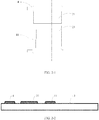
FIG. 1-1 is a top view of a TFT array substrate structure based on OLEDs in accordance with an embodiment of the present disclosure. -
FIG. 1-2 is a cross-sectional view of an electrode structure ofFIG. 1-1 along a section line thereof. -
FIG. 2-1 is a top view of a TFT array substrate structure based on OLEDs in accordance with an embodiment of the present disclosure. -
FIG. 2-2 is a cross-sectional view of an electrode structure ofFIG. 2-1 along a section line thereof. -
FIG. 3-1 is a top view of a TFT array substrate structure based on OLEDs in accordance with an embodiment of the present disclosure. -
FIG. 3-2 is a cross-sectional view of an electrode structure ofFIG. 3-1 along a section line thereof. -
FIG. 4-1 is a top view of a TFT array substrate structure based on OLEDs in accordance with an embodiment of the present disclosure. -
FIG. 4-2 is a cross-sectional view of an electrode structure ofFIG. 4-1 along a section line thereof. -
FIG. 5-1 is a top view of a TFT array substrate structure based on OLEDs in accordance with an embodiment of the present disclosure. -
FIG. 5-2 is a cross-sectional view of an electrode structure ofFIG. 5-1 along a section line thereof. - The present disclosure will now be described in further detail with reference to the accompanying drawings and the embodiments, in which the objects, technical solution, and advantages of the present disclosure will become more apparent from the following description. It is to be understood that the specific embodiments described herein are merely illustrative of the present disclosure and are not intended to limit the present disclosure.
- Specific implementations of the present disclosure will now be described in detail with reference to specific embodiments.
- Referring to
FIGS. 1-1 and1-2 , the present disclosure provides a TFT array substrate structure based on OLEDs. It is to be understood that only an electrode structure corresponding to a pixel is illustrated, and the entire TFT array substrate structure is an array structure with the electrode structure illustrated in the figures as a basic unit. The present embodiment is described on the basis of one basic unit for the sake of clarity. The TFT array substrate structure includes multiple sets of TFT components, capacitors,data signal lines 3, andcommon electrodes 4, all of which are formed on a substrate. The capacitors are coupled to thecommon electrodes 4. Each set of the TFT components includes a driving TFT, and the driving TFT includes a gate, a source, and a drain. A drain frame extends from the drain of the driving TFT and surrounds a pixel block of the TFT array substrate structure. A transparent conductive film is arranged in a region surrounded by the drain frame and is in contact with the drain frame. - Referring further to
FIGS. 1-1 and1-2 , in an embodiment, each set of the TFT components includes a driving TFT and a switch TFT. The switch TFT includes agate 11, asource 12, and adrain 13. For convenient description, the gate, the source, and the drain of the switch TFT are respectively named as a first gate, a first source, and a first drain. The driving TFT includes agate 21, asource 22, and adrain 23. For convenient description, the gate, the source, and the drain of the driving TFT are respectively named as a second gate, a second source, and a second drain. Afirst semiconductor layer 14 is provided between thefirst source 12 and thefirst drain 13, and asecond semiconductor layer 24 is provided between thesecond source 22 and thesecond drain 23. Thefirst source 12, thefirst drain 13, thesecond source 22, and thesecond drain 23 are made of metal, and may be, but not limited to, Al, Mo, Cu, Ti or other metals and alloys, etc. Thefirst source 12 is coupled to thedata signal lines 3. Thefirst drain 13 of the first TFT and thesecond gate 21 of the second TFT are coupled to each other. Aframe 231 extends from thesecond drain 23 and surrounds the pixel block. A transparentconductive film 232 in contact with theframe 231 is arranged in the region enclosed by theframe 231. The transparentconductive film 232 corresponds to the pixel block, and is coupled to an anode or a cathode of an OLED or directly functions as the anode or the cathode of the OLED, so as to apply a driving voltage to the pixel block. - In the embodiment, the drain of the driving TFT is set to be the above-mentioned structure that the drain has the
metal frame 231. The transparentconductive film 232 is arranged in and coupled to theframe 231, and theframe 231 and the transparentconductive film 232 constitute a pixel electrode. Comparing with a pixel electrode only using the transparentconductive film 232 having the same thickness, the resistance of the pixel electrode using themetal frame 231 is significantly reduced. Thus, in the case of the same resistance, the thickness of the transparentconductive film 232 that is coupled to themetal frame 231 is much smaller than that of the transparent conductive film alone. Therefore, in the actual manufacturing, the thickness of the transparent conductive film can be reduced by the arrangement of the metal frame, thereby reducing the manufacturing cost and the possibility of occurrence of a potential defect. In particular, for a flexible display devices, it can prevent the electrode structure from being broken or peeled off during repeated bending, thereby improving the reliability. - In the present embodiment, since the transparent
conductive film 232 is arranged in and coupled to themetal frame 231, the thickness of the transparentconductive film 232 is reduced. The thickness can be generally reduced to 10nm, and usually varies in a range from 10nm to 300nm. While the minimum thickness of a transparent conductive film of a traditional electrode structure is about 70nm. It is apparent that the thickness of the transparentconductive film 232 is greatly reduced, thus a significant effect is provided. Alternatively, the width of themetal frame 231 may be within a range from 1µm to 30µm, further within a range from 1µm to 10µm. The resistance may be greatly reduced without a wide frame, thus the aperture ratio of a display device cannot be reduced. - Furthermore, the detailed structure of the electrode structure is illustrated in
FIG. 1-2 . Thefirst gate 11, thesecond gate 21, and thecommon electrode 4 are arranged at the same layer and directly on a surface of thesubstrate 5. Aninsulation layer 6 is arranged above the layer. Thefirst source 12, thesecond source 22, thefirst drain 13, thesecond drain 23, and the data signalline 3 are arranged at the same layer on theinsulation layer 6. The capacitor is composed of afirst sheet electrode 71 and asecond sheet electrode 72 which are disposed opposite to each other and in parallel. Thefirst sheet electrode 71 is integrally formed with thecommon electrode 4, and thesecond sheet electrode 72 is integrally formed with thefirst drain 13. In addition, the data signalline 3 may be integrally formed with thefirst source 12. The manner of being integrally formed is convenient for implementing process and simplifying the electrode structure, and is convenient for transmission and storage of electrical energy and transmission of drive signals. - Furthermore, a
passivation layer 8 is arranged on thefirst source 12, thesecond source 22, thefirst drain 13, thesecond drain 23, and the data signalline 3. Afirst guide hole 91 is defined in thefirst drain 13, asecond guide hole 92 is defined in thesecond gate 21, athird guide hole 93 is defined in thesecond sheet electrode 72, and afourth guide hole 94 is defined in thesecond source 22. A larger guide hole 95 (95 is not indicated in the figures) is defined in theframe 231 of thesecond drain 23, thereby exposing theframe 231. Thefirst drain 13 and thesecond gate 21 are coupled to each other on thepassivation layer 8 byconductive material 10 that is injected into thefirst guide hole 91 and thesecond guide hole 92. Thesecond sheet electrode 72 and thesecond source 22 are coupled to each other on thepassivation layer 8 by theconductive material 10 that is injected into thethird guide hole 93 and thefourth guide hole 94. - Furthermore, in the present embodiment, a manufacturing process of the TFT array substrate structure is illustrated by taking a double TFT structure as an example, and the following steps are included.
- a, the
first gate 11, thesecond gate 21, and thecommon electrode 4 are formed on thesubstrate 5, as illustrated inFIGS. 2-1 and 2-2 .
Thesubstrate 5 may be made of glass, PET, PI, and the like. Thefirst gate 11 and thesecond gate 21 may be made of Mo, Al, Cu, Cr, Ti, and the like. Thecommon electrode 4 extends from thefirst sheet electrode 71. - b, the
insulation layer 6, afirst semiconductor layer 14, and asecond semiconductor layer 24 are formed, as illustrated inFIGS. 3-1 and 3-2 .
Theinsulation layer 6 is made by a thin film deposition process. The material can be SiNx, SiO2 Al2O3, Resin, and the like. The process can be plasma enhanced chemical vapor deposition (PECVD), sputtering, vapor deposition, spin coating, and the like. Thefirst semiconductor layer 14 and thesecond semiconductor layer 24 are then formed on theinsulation layer 6. Thefirst semiconductor layer 14 is aligned with thefirst gate 11, and thesecond semiconductor layer 24 is aligned with thesecond gate 21. The material of thefirst semiconductor layer 14 and thesecond semiconductor layer 24 may be a-Si, p-Si, metal oxides, organic material, and the like. - c, the
first source 12, thesecond source 22, thefirst drain 13, thesecond drain 23, and the data signalline 3 are formed on theinsulation layer 6, as illustrated inFIGS. 4-1 and4-2 .
The material may be Al, Mo, Cu, Mo/AlNd, Ti, and the like. As illustrated byFIG. 4-1 , thesecond drain 23 formed is illustrated, and theframe 231 extends from thesecond drain 23. The width of theframe 231 is within a range from 1µm to 30µm, preferably within a range from 1µm to 10µm.
The data signalline 3 is integrally formed with thefirst source 12. Thesecond sheet electrode 72 extends from thefirst drain 13. Thesecond sheet electrode 72 and thefirst sheet electrode 71 are disposed opposite to each other and in parallel to form the capacitor. - d, the
passivation layer 8 is formed on thefirst source 12, thesecond source 22, thefirst drain 13, thesecond drain 23, and the data signalline 3, as illustrated inFIGS. 5-1 and 5-2 .
Thepassivation layer 8 is formed by way of deposition, and the material can be SiNx, SiO2 Resin, etc. Guide holes are defined in thefirst drain 13, thesecond gate 21, thesecond source 22, thesecond sheet 72, and theframe 231 of thesecond drain 23. Theframe 231 defines a larger guide hole so that theframe 231 is exposed, and the exposed portion corresponds to the OLED pixel block. - e, a transparent pixel electrode is formed and necessary electrical connections are realized, as illustrated in
FIGS. 1-1 and1-2 . - The transparent
conductive material 10 is deposited on thepassivation layer 8, such as ITO, IZO, etc. The transparentconductive material 10 fills the guide holes, and the transparentconductive film 232 is formed in theframe 231. The transparentconductive material 10 is etched to form the structure illustrated inFIG. 1-1 , in which thefirst drain 13 and thesecond gate 21 are coupled to each other, thesecond source 22 and thesecond sheet electrode 72 are coupled to each other, and the transparentconductive film 232 in theframe 231 is a pixel electrode for supplying a voltage to the OLED. The structure is suitable for a bottom emission mode. - The TFT array substrate structure of the embodiment of the present disclosure is suitable for use in an OLED display device. The thickness of the transparent conductive film is reduced due to the existence of the metal drain frame, thereby reducing the manufacturing cost of the OLED display device, avoiding the defect that electrodes are peeled off when the flexible OLED display screen is bent, and improving the reliability of the OLED display screen.
- The foregoing descriptions are only preferred embodiments of the present disclosure, and is not intended to limit the present disclosure. Any modifications, equivalent replacements, and improvements made within the spirit and principle of the present disclosure shall fall within the protection scope of the present disclosure.
Claims (8)
- A thin film transistor (TFT) array substrate structure based on organic light-emitting diodes (OLEDs), comprising:a plurality of sets of TFT components;capacitors;common electrodes; anddata signal lines, wherein the plurality of sets of the TFT components, the capacitors, the common electrodes, and the data signal lines are formed on a substrate, each of the plurality of sets of the TFT components comprises a driving TFT, and the driving TFT comprises a gate, a source, and a drain, wherein a drain frame extends from the drain and surrounds a pixel block of the TFT array substrate structure, and a transparent conductive film is arranged in a region surrounded by the drain frame and is in contact with the drain frame.
- The TFT array substrate structure of claim 1, characterized in that each of the plurality of sets of the TFT components further comprises a switch TFT, the switch TFT comprises a gate, a source, and a drain, the source of the switch TFT is coupled to the data signal line, and the drain of the switch TFT is coupled to the gate of the driving TFT.
- The electrode structure of claim 2, characterized in that the capacitor comprises a first sheet electrode and a second sheet electrode that are disposed opposite to each other and in parallel, the gate of the switch TFT, the gate of the driving TFT, the common electrode, and the first sheet electrode are arranged at a same layer on a surface of the substrate, the source and the drain of the switch TFT, the source and the drain of the driving TFT, the data signal line, and the second sheet electrode are arranged at a same layer, and separated from the layer where the gate of the switch TFT, the gate of the driving TFT, the common electrode, and the first sheet electrode are located by an insulation layer.
- The electrode structure of claim 3, characterized in that the data signal line is coupled to the source of the switch TFT to form an integral whole.
- The electrode structure of claim 3, characterized in that the common electrode is coupled to the first sheet electrode to form an integral whole, and the drain of the switch TFT is coupled to the second sheet electrode to form an integral whole.
- The electrode structure of any of claims 1-5, characterized in that the drain frame has a width within a range from 1µm to 30µm.
- The electrode structure of claim 6, characterized in that the drain frame has a width within a range from 1µm to 10µm.
- The electrode structure of any of claims 1-5, characterized in that the transparent conductive film has a width within a range from 10nm to 300nm.
Applications Claiming Priority (1)
| Application Number | Priority Date | Filing Date | Title |
|---|---|---|---|
| PCT/CN2014/091176 WO2016074241A1 (en) | 2014-11-14 | 2014-11-14 | Tft array substrate structure based on oled |
Publications (2)
| Publication Number | Publication Date |
|---|---|
| EP3220422A1 true EP3220422A1 (en) | 2017-09-20 |
| EP3220422A4 EP3220422A4 (en) | 2018-09-12 |
Family
ID=55953631
Family Applications (1)
| Application Number | Title | Priority Date | Filing Date |
|---|---|---|---|
| EP14905996.6A Withdrawn EP3220422A4 (en) | 2014-11-14 | 2014-11-14 | Tft array substrate structure based on oled |
Country Status (6)
| Country | Link |
|---|---|
| US (1) | US10163998B2 (en) |
| EP (1) | EP3220422A4 (en) |
| JP (1) | JP6503066B2 (en) |
| KR (1) | KR101968431B1 (en) |
| CN (1) | CN105765724A (en) |
| WO (1) | WO2016074241A1 (en) |
Families Citing this family (5)
| Publication number | Priority date | Publication date | Assignee | Title |
|---|---|---|---|---|
| WO2018232698A1 (en) * | 2017-06-22 | 2018-12-27 | 深圳市柔宇科技有限公司 | Apparatus for manufacturing array substrate and method for manufacturing array substrate |
| KR102427666B1 (en) * | 2019-05-23 | 2022-08-02 | 삼성디스플레이 주식회사 | Organic light-emitting device and apparatus including the same |
| EP4651686A3 (en) | 2020-01-28 | 2026-02-25 | OLEDWorks LLC | Stacked oled microdisplay with low-voltage silicon backplane |
| KR102866834B1 (en) | 2020-08-19 | 2025-09-30 | 오엘이디워크스 엘엘씨 | Pixel circuitry for crosstalk reduction |
| US12245473B2 (en) * | 2020-09-24 | 2025-03-04 | Chengdu Boe Optoelectronics Technology Co., Ltd. | Display panel, display device and manufacturing method thereof |
Family Cites Families (17)
| Publication number | Priority date | Publication date | Assignee | Title |
|---|---|---|---|---|
| JP5408829B2 (en) * | 1999-12-28 | 2014-02-05 | ゲットナー・ファンデーション・エルエルシー | Method for manufacturing active matrix substrate |
| JP2003043410A (en) * | 2001-07-27 | 2003-02-13 | Mariiasshu:Kk | Kaleidoscope |
| AU2003260959A1 (en) | 2002-09-11 | 2004-04-30 | Semiconductor Energy Laboratory Co., Ltd. | Light-emitting apparatus and fabrication method of the same |
| KR100579184B1 (en) * | 2003-11-24 | 2006-05-11 | 삼성에스디아이 주식회사 | Organic light emitting display device |
| TWI292281B (en) | 2005-12-29 | 2008-01-01 | Ind Tech Res Inst | Pixel structure of active organic light emitting diode and method of fabricating the same |
| JP2007333808A (en) * | 2006-06-12 | 2007-12-27 | Mitsubishi Electric Corp | Active matrix display device |
| KR101015850B1 (en) * | 2009-02-09 | 2011-02-24 | 삼성모바일디스플레이주식회사 | Organic light emitting display device manufacturing method |
| JP2010251156A (en) | 2009-04-16 | 2010-11-04 | Panasonic Corp | Color organic electroluminescence display device and manufacturing method thereof |
| JP2011100938A (en) * | 2009-11-09 | 2011-05-19 | Nippon Shokubai Co Ltd | ORGANIC LIGHT EMITTING ELEMENT, DISPLAY DEVICE USING THE ORGANIC LIGHT EMITTING ELEMENT, AND ELECTRONIC DEVICE |
| KR101074803B1 (en) * | 2009-11-24 | 2011-10-19 | 삼성모바일디스플레이주식회사 | Organic light emitting display apparatus and method of manufacturing thereof |
| KR101155903B1 (en) | 2010-03-09 | 2012-06-21 | 삼성모바일디스플레이주식회사 | Organic light emitting diode display and method for manufacturing the same |
| KR20110134685A (en) * | 2010-06-09 | 2011-12-15 | 삼성모바일디스플레이주식회사 | Display device and manufacturing method thereof |
| KR101824537B1 (en) * | 2010-10-01 | 2018-03-15 | 삼성디스플레이 주식회사 | Thin film transistor and organic light emitting display |
| KR101889918B1 (en) * | 2010-12-14 | 2018-09-21 | 삼성디스플레이 주식회사 | Organinc light emitting display device and manufacturing method for the same |
| KR101902922B1 (en) * | 2011-03-03 | 2018-10-02 | 삼성전자주식회사 | Thin film transistor and manufacturing method of the same |
| TWI483344B (en) * | 2011-11-28 | 2015-05-01 | 友達光電股份有限公司 | Array substrate and manufacturing method thereof |
| TWI479663B (en) * | 2011-12-22 | 2015-04-01 | 友達光電股份有限公司 | Array substrate and manufacturing method thereof |
-
2014
- 2014-11-14 EP EP14905996.6A patent/EP3220422A4/en not_active Withdrawn
- 2014-11-14 KR KR1020177014976A patent/KR101968431B1/en not_active Expired - Fee Related
- 2014-11-14 WO PCT/CN2014/091176 patent/WO2016074241A1/en not_active Ceased
- 2014-11-14 US US15/524,071 patent/US10163998B2/en not_active Expired - Fee Related
- 2014-11-14 CN CN201480003352.0A patent/CN105765724A/en active Pending
- 2014-11-14 JP JP2017525814A patent/JP6503066B2/en not_active Expired - Fee Related
Also Published As
| Publication number | Publication date |
|---|---|
| EP3220422A4 (en) | 2018-09-12 |
| WO2016074241A1 (en) | 2016-05-19 |
| US10163998B2 (en) | 2018-12-25 |
| US20170352715A1 (en) | 2017-12-07 |
| CN105765724A (en) | 2016-07-13 |
| JP2018502316A (en) | 2018-01-25 |
| KR20170081668A (en) | 2017-07-12 |
| JP6503066B2 (en) | 2019-04-17 |
| KR101968431B1 (en) | 2019-04-11 |
Similar Documents
| Publication | Publication Date | Title |
|---|---|---|
| CN106409869B (en) | Organic Light Emitting Diode Display | |
| EP2889866B1 (en) | Flexible display device and method for fabricating the same | |
| CN104953044B (en) | flexible OLED and preparation method thereof | |
| CN105280669B (en) | Display device | |
| KR102740671B1 (en) | Display device and method for manufacturing of the same | |
| US10734608B2 (en) | Display panel and manufacturing method thereof and display device including display panel | |
| US20160380239A1 (en) | Method for manufacturing amoled display device and structure thereof | |
| KR20130013515A (en) | Organic light emitting display apparatus | |
| CN113745265B (en) | Micro LED display panel and preparation method thereof | |
| US10020324B2 (en) | Display device | |
| KR102580063B1 (en) | Display device and method for fabricating the same | |
| US10163998B2 (en) | TFT array substrate structure based on OLED | |
| WO2019064365A1 (en) | Flexible display device and method for manufacturing flexile display device | |
| US9553197B2 (en) | Thin film transistor and display device including the same | |
| US20140191210A1 (en) | Organic light-emitting diode device | |
| KR102587876B1 (en) | Organic Light Emitting Display device having a repair area | |
| KR102194667B1 (en) | Organic light emitting display device and method for manufacturing the same | |
| US20190362656A1 (en) | Flexible display device and method for manufacturing flexible display device | |
| CN113629073B (en) | TFT backplane and display panel | |
| US20140183520A1 (en) | Oxide thin film transistor structure and method thereof | |
| KR102049601B1 (en) | Organic light emitting diode display device and fabricating method of the same | |
| US20140027761A1 (en) | Thin film transistor substrate, display thereof and manufacturing method thereof | |
| US9159775B1 (en) | Anode connection structure of organic light-emitting diode and manufacturing method thereof | |
| JP2021162639A (en) | Active matrix substrate and display device | |
| KR20120063784A (en) | Thin film transistor substrate and method for fabricating the same |
Legal Events
| Date | Code | Title | Description |
|---|---|---|---|
| PUAI | Public reference made under article 153(3) epc to a published international application that has entered the european phase |
Free format text: ORIGINAL CODE: 0009012 |
|
| 17P | Request for examination filed |
Effective date: 20170515 |
|
| AK | Designated contracting states |
Kind code of ref document: A1 Designated state(s): AL AT BE BG CH CY CZ DE DK EE ES FI FR GB GR HR HU IE IS IT LI LT LU LV MC MK MT NL NO PL PT RO RS SE SI SK SM TR |
|
| AX | Request for extension of the european patent |
Extension state: BA ME |
|
| DAX | Request for extension of the european patent (deleted) | ||
| A4 | Supplementary search report drawn up and despatched |
Effective date: 20180814 |
|
| RIC1 | Information provided on ipc code assigned before grant |
Ipc: H01L 27/32 20060101AFI20180808BHEP |
|
| STAA | Information on the status of an ep patent application or granted ep patent |
Free format text: STATUS: THE APPLICATION HAS BEEN WITHDRAWN |
|
| 18W | Application withdrawn |
Effective date: 20191016 |