EP3220391A1 - Reference generation for high density two state resistance change memories - Google Patents
Reference generation for high density two state resistance change memories Download PDFInfo
- Publication number
- EP3220391A1 EP3220391A1 EP17161286.4A EP17161286A EP3220391A1 EP 3220391 A1 EP3220391 A1 EP 3220391A1 EP 17161286 A EP17161286 A EP 17161286A EP 3220391 A1 EP3220391 A1 EP 3220391A1
- Authority
- EP
- European Patent Office
- Prior art keywords
- memory
- charge
- state
- cells
- arrangement
- Prior art date
- Legal status (The legal status is an assumption and is not a legal conclusion. Google has not performed a legal analysis and makes no representation as to the accuracy of the status listed.)
- Granted
Links
Images






Classifications
-
- G—PHYSICS
- G11—INFORMATION STORAGE
- G11C—STATIC STORES
- G11C13/00—Digital stores characterised by the use of storage elements not covered by groups G11C11/00, G11C23/00, or G11C25/00
- G11C13/0002—Digital stores characterised by the use of storage elements not covered by groups G11C11/00, G11C23/00, or G11C25/00 using resistive RAM [RRAM] elements
- G11C13/0021—Auxiliary circuits
- G11C13/004—Reading or sensing circuits or methods
-
- G—PHYSICS
- G11—INFORMATION STORAGE
- G11C—STATIC STORES
- G11C11/00—Digital stores characterised by the use of particular electric or magnetic storage elements; Storage elements therefor
- G11C11/02—Digital stores characterised by the use of particular electric or magnetic storage elements; Storage elements therefor using magnetic elements
- G11C11/16—Digital stores characterised by the use of particular electric or magnetic storage elements; Storage elements therefor using magnetic elements using elements in which the storage effect is based on magnetic spin effect
- G11C11/165—Auxiliary circuits
- G11C11/1673—Reading or sensing circuits or methods
-
- G—PHYSICS
- G11—INFORMATION STORAGE
- G11C—STATIC STORES
- G11C13/00—Digital stores characterised by the use of storage elements not covered by groups G11C11/00, G11C23/00, or G11C25/00
- G11C13/0002—Digital stores characterised by the use of storage elements not covered by groups G11C11/00, G11C23/00, or G11C25/00 using resistive RAM [RRAM] elements
- G11C13/0021—Auxiliary circuits
- G11C13/0023—Address circuits or decoders
- G11C13/0026—Bit-line or column circuits
-
- G—PHYSICS
- G11—INFORMATION STORAGE
- G11C—STATIC STORES
- G11C13/00—Digital stores characterised by the use of storage elements not covered by groups G11C11/00, G11C23/00, or G11C25/00
- G11C13/0002—Digital stores characterised by the use of storage elements not covered by groups G11C11/00, G11C23/00, or G11C25/00 using resistive RAM [RRAM] elements
- G11C13/0021—Auxiliary circuits
- G11C13/0033—Disturbance prevention or evaluation; Refreshing of disturbed memory data
-
- G—PHYSICS
- G11—INFORMATION STORAGE
- G11C—STATIC STORES
- G11C13/00—Digital stores characterised by the use of storage elements not covered by groups G11C11/00, G11C23/00, or G11C25/00
- G11C13/0002—Digital stores characterised by the use of storage elements not covered by groups G11C11/00, G11C23/00, or G11C25/00 using resistive RAM [RRAM] elements
- G11C13/0021—Auxiliary circuits
- G11C13/0097—Erasing, e.g. resetting, circuits or methods
-
- G—PHYSICS
- G11—INFORMATION STORAGE
- G11C—STATIC STORES
- G11C13/00—Digital stores characterised by the use of storage elements not covered by groups G11C11/00, G11C23/00, or G11C25/00
- G11C13/04—Digital stores characterised by the use of storage elements not covered by groups G11C11/00, G11C23/00, or G11C25/00 using optical elements ; using other beam accessed elements, e.g. electron or ion beam
-
- G—PHYSICS
- G11—INFORMATION STORAGE
- G11C—STATIC STORES
- G11C7/00—Arrangements for writing information into, or reading information out from, a digital store
- G11C7/06—Sense amplifiers; Associated circuits, e.g. timing or triggering circuits
- G11C7/065—Differential amplifiers of latching type
-
- G—PHYSICS
- G11—INFORMATION STORAGE
- G11C—STATIC STORES
- G11C13/00—Digital stores characterised by the use of storage elements not covered by groups G11C11/00, G11C23/00, or G11C25/00
- G11C13/0002—Digital stores characterised by the use of storage elements not covered by groups G11C11/00, G11C23/00, or G11C25/00 using resistive RAM [RRAM] elements
- G11C13/0021—Auxiliary circuits
- G11C13/004—Reading or sensing circuits or methods
- G11C2013/0054—Read is performed on a reference element, e.g. cell, and the reference sensed value is used to compare the sensed value of the selected cell
Definitions
- the invention relates to the field of memories. More particularly, the present invention relates to the field of memories based on two state resistance change memories such as STT-MRAM and RRAM, as well as to systems and methods for creating a reference signal for evaluating two state resistance change memories.
- the yield of the memory is typically improved by redundancy. More particularly, additional memory elements are provided to cope with a situation wherein one or more memory elements are broken, e.g. wherein memory elements are defect due to a stuck at 0/1 fault.
- the present invention relates to a memory arrangement comprising a plurality of memory cells arranged in an array structure, wherein each memory cell comprises a memory element being a two state resistance change memory element, the memory arrangement comprising crossing word and bit lines and each memory cell is being connected between a different crossing of a word line and a bit line, the memory cells furthermore being connectable to a source line, each bit line has a bit line capacitance, for storing a charge representative of the state of a selected memory element, a set of at least two memory cells, positioned at different bit lines but on the same word line, are being defined as reference cells, one reference cell being set in a high resistance state and a second reference cell being in a low resistance state, at least those bit lines wherein the reference cells are defined furthermore are interconnected by an equalizing switch, for equalizing the charges on the bit line capacitance of said at least two bit lines.
- the charge representative of the state of a selected memory element may be defined when current is running through the selected memory element.
- the latter may be when current is flowing between the bit line and the ground, e.g. leading to a discharge of the capacitance.
- the latter may be when current is flowing between the bit line and a voltage source, which may result in a charging or a discharging of the capacitance.
- the bit line capacitance may be a capacitance may be created by the memory element and the wiring of the bit line itself. In some embodiments also an explicit bit cell capacitor may be present.
- the number of cells may be two or higher.
- the number of reference cells used typically may be an even number, so that the average typically equals the midpoint between a high and a low resistance state. Nevertheless, weighing factors could be introduced so that, when using an odd number of reference cells, the midpoint of all reference cells also results in the midpoint between a high and a low resistance state.
- the memory arrangement furthermore may comprise a sense amplifier for reading the state of a selected memory element, different from the cells defined as reference cells, said sense amplifier being configured for using the equalized charge on the bit line capacitors as a reference signal and further configured for using the charge of the selected memory element for reading the state.
- the sensing amplifier is thus configured for reading the state of the selected memory element.
- the bit lines whereon the memory elements are positioned are connectable to the sense amplifier inputs and thus can be connected for sensing the charge for the selected memory element. Combined with the equalized charge from the reference cells, the sensing amplifier provides an output representative of the state of the selected memory element.
- the equalizing switch may comprise a Field Effect Transistor (FET).
- FET Field Effect Transistor
- the FET may be a MOSFET being P or N, or a passgate using P and N MOST.
- the switch should not leak the equalized charge during the read cycle.
- the memory elements may be STT-MRAM memory elements or RRAM memory elements.
- the memory elements may be connected to the bit line using a selection switch for selectively contacting the memory elements with the supply line during a pre-charge phase thereof.
- the reference cells as well as the cells to be read can be connected between the supply and the ground by a switch only during the pre-charge phase, rather than being continuously connected.
- the latter advantageously results in the possibility of having a low power operation.
- the charge may be created when the current flows from the source line to the bit line through the memory element.
- the cells when the memory cells are not active, the cells can be disconnected so that no current flows and power is saved. Since advantageously current only flows through the memory cells during the pre-charge phase, full swing VDD dynamic signal range can be obtained. The current thus only flows during one phase of the read cycle.
- the switching during pre-charge may be performed using a single switch for the reference cells and a single switch for the cell to be read, each switch connecting a bit line to the sensing amplifier. The switching thus may be performed using only two switches per sensing amplifier.
- the charges of the memory cells that are created during a pre-charge phase are equalized.
- the charges of the memory cells are typically no longer being pre-charged and the connectable is disconnected. So no more current flows between the supply and the ground line.
- the memory arrangement may comprise a memory controller for dynamically selecting the reference cells used.
- the controller may further control the pre-charging of the memory cells, through the selection switch, as well as the operation of the sensing amplifier depending on the architecture.
- the controller also may control the connecting means to the source line, the activation of the sensing amplifier, the selection of Word lines, Bit lines, etc.
- the equalizing switches may be positioned between more than those bit lines comprising the reference cells, and the reference cells can be selected to be cells in those bit lines interconnected via equalizing switches.
- Such a selection may be dynamically, e.g. using a memory controller, or may be performed during a calibration or correction procedure.
- the memory arrangement may comprise reference cells in each of the bit lines, whereby each of the bit lines is interconnected by equalizing switches to another bit line.
- the memory arrangement may comprise a first sub-arrangement and a second sub-arrangement, each of said sub-arrangements being connected to the sense amplifier through a multiplexer, comprising distinct word lines and comprising a same number of bit lines, wherein the reference cells are all defined/positioned in one sub-arrangement selected by a given Word line, and the selected memory element is in the other sub-arrangement.
- the multiplexer may be an array of switches.
- the multiplexer may be an analog multiplexer.
- the use of distinct word lines allows a controller to select the reference cells independently from the selected cell to be read. In the present embodiment, the bit lines are not shared over the different sub-arrangements.
- the memory arrangement may comprises at least a first and a second sub-arrangement, each sub-arrangement being connected to a sense amplifier through a multiplexer and sharing word lines with another sub-arrangement wherein the reference elements are positioned in two bit lines, each bit line belonging to a different sub-arrangement and wherein the reference signal is generated based on an equalized charge in said two bit lines being positioned in the different sub-arrangements, and the selected memory element is located in each sub-array and connected to a bit line different from the reference elements.
- the reference voltage typically thus is the voltage after charge redistribution by the equalizing switches.
- the multiplexer may be an array of switches.
- the multiplexer may be an analog multiplexer. It is an advantage of embodiments of the present invention that the memory arrangement using shared reference bit lines does not require a separate multiplexing cycle to share the charge between the sense-amplifier since it can be done while the word line is fired. Consequently, such an implementation results in a fast sensing process.
- the memory arrangement furthermore may comprises a memory controller for detecting a stuck at 0/1 error in a memory cell, the controller further reserving the stuck at 0/1 memory cell for reference cell purpose (only) and for altering the state of the non stuck at 0/1 the reference cells so as to include the state of the memory cell comprising the stuck at 0/1 error.
- a memory controller for detecting a stuck at 0/1 error in a memory cell, the controller further reserving the stuck at 0/1 memory cell for reference cell purpose (only) and for altering the state of the non stuck at 0/1 the reference cells so as to include the state of the memory cell comprising the stuck at 0/1 error.
- a multiplexer may be used for multiplexing memory elements along bit lines of the memory arrangement, whereby the multiplexer is arranged for selecting a bit line potential of the selected memory element and transferring a corresponding charge to the sense amplifier.
- the controller also typically control the multiplexer.
- the multiplexing principle can be applied with a multiplexing number being 2 or higher.
- the multiplexing number is not a limiting factor for embodiments of the present invention.
- a multiplexer may be used for multiplexing memory elements along bit lines of the memory arrangement, whereby the multiplexer is arranged for selecting a bit line potential of the reference signal and transferring it to the sense amplifier.
- the memory arrangement may be adapted for using an n-bit word in memory cells along a word line as reference, and wherein the system comprises a memory controller for dynamically altering the n-bit word used as reference.
- the bit line potential may be transferred by a transfer switch to the sense amplifier.
- the transfer switches, the selection switches, the switches in the multiplexer, and/or the equalizing switches may be any of a transmission gate, a PFET or an NFET.
- the present invention also relates to a method for sensing a state of a two state resistance change memory element, the method comprising
- Selecting at least two reference cells may mean activating the selection switch and charging the bit line.
- the reference cell may be set, during a set phase or write phase, prior to the reading phase, to a high resistance state and a second reference cell may be set during a set phase or write phase, prior to the reading phase, to a low resistance state.
- this refers to equalization of the charges of the reference cells created during the pre-charge action by closing the selection switch.
- selecting the memory element to be sensed may be done at the same time as the first selecting, i.e. as the selecting of the at least two reference cells.
- Evaluating the sensing charge in the sensing amplifier as function of the reference equalized charge may be comparing the sensed charge and the reference charge by the sensing amplifier.
- the method comprises equalizing a plurality of reference cells in one word line and providing the equalized charge to the sensing amplifier through a multiplexer and selecting a memory element in another word line, sensing a charge and providing the corresponding sensing charge signal through a separate multiplexer to the sensing amplifier, so that the equalized charge and the sensing charge can be compared for evaluating the sensing charge.
- the method comprises equalizing charge of a plurality of reference cells positioned in different sub-arrangements for generating an equalized charged, and sensing a sensing charge for a memory element in one of the sub-arrangements and comparing the sensing charge and the equalized charged in a sensing amplifier of the specific sub-arrangement.
- the present invention furthermore relates to the use of a memory arrangement as described above for storing and/or reading out data stored in the memory arrangement.
- storing and/or reading out data are known by the person skilled in the art.
- the memory arrangement will be shown, for ease of illustration, as a set of memory elements logically organized in rows and columns.
- the terms “horizontal” and “vertical” (related to the terms “row” and “column” respectively) are used to provide a co-ordinate system and for ease of explanation only. They do not need to, but may, refer to an actual physical direction of the device.
- the terms “column” and “row” are used to describe sets of array elements which are linked together.
- the linking can be in the form of a Cartesian array of rows and columns; however, the present invention is not limited thereto. As will be understood by those skilled in the art, columns and rows can be easily interchanged and it is intended in this disclosure that these terms be interchangeable.
- non-Cartesian arrays may be constructed and are included within the scope of the invention. Accordingly the terms “row” and “column” should be interpreted widely. To facilitate in this wide interpretation, the claims refer to logically organised in rows and columns. By this is meant that sets of ... are linked together in a topologically linear intersecting manner; however, that the physical or topographical arrangement need not be so.
- the rows may be circles and the columns radii of these circles and the circles and radii are described in this invention as "logically organised" rows and columns. Also, specific names of the various lines, e.g.
- word line and bit line are intended to be generic names used to facilitate the explanation and to refer to a particular function and this specific choice of words is not intended to in any way limit the invention. It should be understood that all these terms are used only to facilitate a better understanding of the specific structure being described, and are in no way intended to limit the invention.
- the present invention relates to a memory arrangement for memory cells based on two state resistance change memory elements.
- Such memory cells typically are arranged in an array structure and comprise crossing word lines and bit lines.
- the word lines will be shown as horizontally oriented lines and the bit lines will be shown as vertically oriented lines, but as indicated above other orientations are also possible.
- Each memory cell is connected between a crossing word and bit line.
- the memory cells are also connected to a source line.
- the word line is connected to supply current during read-operation.
- the bit line is pre-charged to known supply voltage of VDD before word-line is asserted.
- the stored charge over bit-line capacitor is discharged and the current will depend on the state of the memory element (R H or R L ) and this current (I H or I L ) will flow from the bit-line to the source line.
- this current I H or I L
- another known supply voltage I used and the bit line capacitor can be further charged.
- Each bit line comprises a bit line capacitance C b for storing a charge representative of the state of a selected memory element.
- the charge on the bit line capacitance is discharged when current flows from the bit line to the source line or to ground and is influenced by the state, i.e. the resistance, of the memory element.
- the charge on the bit line capacitance is charged when current flows from the bit line to the source line.
- the source line may therefore be connected to a predetermined voltage. It is to be noted that the bit line capacitance remains the same across the array for the same number of cells per column.
- the memory cells comprise memory elements being two state resistance change memory element.
- the resistance change is stored as a state.
- Such cells have two possible states, often referred to as a high state and a low state.
- states shall, where appropriate, be indicated as R H and R L .
- At least two memory cells being positioned at different bit lines, are defined, e.g. selected, as reference cells.
- One reference cell thereby is set in a high resistance change mode, while a second reference cell is being set in a low resistance change mode.
- the reference cells correspond with memory cells that are in principle settable to any state, but for the purpose as being used as reference cells these cells are set in advance such that the average charge that will be "sensed" during the pre-charge phase is an average of the high and the low state. If for example two cells are used, typically one cell is set to a high state and one is set to a low state, so that the equalization results in an average of the high and the low state.
- the memory arrangement thus is put in a particular state prior to the pre-charge.
- At least those bit lines wherein the at least two reference cells are positioned furthermore are interconnected using an equalizing switch for equalizing a charge on the bit line capacitors of said at least two bit lines, when the reference cells have been read out.
- a reference signal thus is generated through at least two, advantageously neighbouring, reference elements, one of them being set having a high resistance R H and one of them being set as having a low resistance state R L . It will be understood that while the example is given for a configuration where discharging of the capacitance is used, the same reasoning will be mutates mutandis applicable when charging of the capacitance is used.
- a sensing amplifier may be used which makes use of a reference signal being equal to or based on the effective equalized charge.
- the sensing amplifier is thus configured for reading the state of the selected memory element.
- the bit lines whereon the memory elements are positioned are connectable to the sense amplifier inputs and thus can be connected for sensing the charge for the selected memory element. Combined with the equalized charge from the reference cells, the sensing amplifier provides an output representative of the state of the selected memory element.
- the equalizing switch can for example be designed by a transmission gate, a PFET or an NFET. In advantageous embodiments, the equalizing switch can be an NFET.
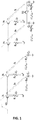
- FIG. 1 illustrates part of a memory arrangement.
- the system illustrates two memory cells positioned on a single word line WL(1) both connected to a bit line BL at a supply voltage V.
- the two memory cells are selected as reference cells.
- the cells are set to a high resistance change state and a low resistance change state.
- a bit line capacitor C b is present wherein the charge created during pre-charged phase is stored.
- FIG. 1 On the left hand side of FIG. 1 , the situation is shown wherein no equalizing switch is present.
- the resulting current flowing from the bit-line to source line is I H and the corresponding charge discharged from the bit line capacitor in Q H
- the resulting current flowing from the bit line to the source line is I L and the corresponding charge discharged from the bit line capacitor is Q L
- an equalizing switch is positioned between the two bit lines wherein the reference cells are positioned.
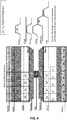
- FIG. 2 illustrates an open bit-line architecture implementation according to an embodiment of the present invention.
- the memory arrangement comprises an even number of bit lines (columns).
- a word line WL[0] is fired to read the word in the word line.
- the state of each individual memory element results in a discharge of a charge from the bit line capacitance.
- the word from the portion indicated by slice 0, is thus read by asserting WL[0], but in order to appropriately assess, a reference is used generated in slice 1 by asserting the equalizing signal and the reference word line RWL[1] corresponding with a word line wherein reference cells are positioned, with a predetermined memory state.
- the equalizing signal results in the charge sharing as illustrated in FIG.
- the resulting reference signal for each of the bit lines is "C bl x Vdd - 0,5 x (Q H + Q L )".
- the date in the reference word line therefore are an equal number (equal to the number of elements to be assessed in the word line of slice 0) of RH and RL state elements are used.
- the equalizing switch is only shown for the first and second bit line, but typically may be applied to all bit lines.
- the transistors T1 and T2 are equalizing switches implemented using NFET. If these would be implemented in PFET, then the polarity of the equalizing signal will be active-low.
- the equalizing signal EQ(1) is thus used to share charge across slice 1, in order to average out the effective charge deposited per bit line.
- the system shown in the example of FIG. 2 is symmetrical, so if any row is to be read in slice 1, the reference signal can be generated in slice 0. It is to be noticed that the invention is not limited thereto and that also an asymmetric arrangement can be used, whereby there are only memory elements that are not reference elements in one of the slices and whereby the other slice is purely used as reference signal generating element. It is to be noticed that according to embodiments of the present invention, any row in the array can be used as reference word line RWL.
- the memory arrangement may for example comprise a memory controller for assigning a reference row dynamically during the life of the memory.
- a sensing means e.g. a sensing amplifier.
- a sensing amplifier For the sake of completeness, one example of a sensing amplifier is shown in FIG. 3 , but any sensing means allowing to evaluate a signal as function of a reference signal may be used.
- the charge averaging principle applied to a 32 bit arrangement will be discussed below. If for example there are 32 bits in a word for an open-bit-line architecture as shown in FIG. 2 , the situation can be as follows : If all reference cell states exactly match then the effective charge on a 32 bit-line can be calculates as "32 x [C bl x Vdd - 0,5 x (Q H + Q L )]", which results in a charge per bit-line as "32 x [C bl x Vdd - 0,5 x (Q H + Q L )]/32".
- the averaging is done over all bit lines, so according to embodiments the charge is equalized over at least two cells, but may be equalized over more than two cells.
- this may be done in couples of cells in a high and a low resistance state, but it could alternatively even be done for reference cells whereby a different number of reference cells with a high resistance state compared to a low resistance state is used, provided the equalizing compensates for such different numbers.
- the 32 bit-line example if there is a mismatch in one of the reference cells, for example if one of the reference cell resistances has changed from RH to (RH+ ⁇ RH), this results in charge change written as (QH- ⁇ QH).
- the memory arrangement follows a simple design and does not require analog referencing. This avoids the need for input output transistors and higher supplies. Moreover the referencing system/method is simplified. Since the references are averaged, the accuracy is increased. It is to be noted that at pitch sense - amplifiers without multiplexing are possible, comparable to the situation with DRAM. The specific arrangement requires double access power, which is not the case for some embodiments described below.
- FIG. 4 one example of an implementation is shown wherein multiplexing is used.
- the latter is advantageous since it allows to use a single sensing means for the different bit lines to be read out.
- the memory arrangement shown is similar to the arrangement shown in FIG. 2 , except in that the different sensing amplifiers are replaced by a single sensing amplifier that is connected to the different bit lines of the memory cells to be read out and the reference memory cells by multiplexers.
- the implementation shown requires that there are two multiplexers.
- the equalizing signal EQ[0] in slice 0 is not applied, since no reference signals are to be measured in slice 0 (the reference measurements are made in slice 1).
- the reference word line WL[1], also referred to as WLR[1] and the equalizing signal is driven during a time ⁇ t so as to share charge over the reference elements. Thereafter, during a time ⁇ t1, the charge is shared between the nodes of the sensing means and the reference bit line, so as to provide the sensing means with an appropriate reference signal.
- the sensing means senses the state of the memory element of interest in slice 0.
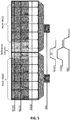
- a closed bit line multiplexing implementation is described. An example thereof is shown in FIG. 5 .
- the memory arrangement is adapted for sensing, whereby two sub-arrangements of memory elements are provided arranged such that each sub-arrangement has different bit lines, but that these share the word lines.
- Each sub-arrangement has a separate multiplexer and in each of these sub arrangements memory elements to be sensed and reference memory elements are present.
- the reference is generated out of two reference column cells for sensing two bits.
- Each of the reference column (bit line wherein the reference element is positioned), belongs to a different sub-arrangement, but the reference columns share charge using an equalizing switch.
- the reference word line RWL is not required to generate the reference charge (the reference elements are positioned on the word line where also memory cells to be measured are positioned.
- the two reference bit lines RBL[0] and RBL[1] are the reference bit-lines used for generating a reference per multiplexer.
- the averaging of charge can be achieved by adding equalizer transistors between the two reference bit-lines RBL (or if more reference bit lines are used between all reference bit-lines RBL).
- the word line is fired for a period in time resulting in charge generation, both for memory cells to be read as for reference cells.
- the equalizing switch is operated so that charge sharing occurs for the bit lines of the reference cells.
- the sensing means is initiated, allowing sensing of the memory cells to be evaluated as function of the reference signal. Since no separate cycle is required for sharing the charge in the reference cells because it can be done while the word line is fired, this results in a fast system, compared to the system shown in FIG. 4 .
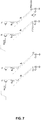
- FIG. 6 an alternative (compared to FIG. 1 ) memory arrangement is shown in FIG. 6 , wherein precharging via the source line is performed.
- the latter is obtained by implementing a voltage per bit line instead of applying a sensing current.
- Precharging can be performed using a voltage Vdd, resulting in an additional charge Cs*Vdd being present on the capacitor.
- the initial charge may correspond with the initial charge Cs*Vdd to maximize the range to Vdd or Vss, but can be different.
- the resulting charge then is a combination of the source line discharge from VDD and the charge induced by the resistance of the reference elements, resulting in C S V dd ⁇ Q H + Q L 2
- a charging of the bitline from source line is performed.
- the resulting charge then is the charge deposited by the resistance of the reference elements, resulting in Q H + Q L 2 .
- the present invention relates to a method for sensing a state of a two state resistance change memory element.
- the method may be advantageously implemented for a memory arrangement as described above.
- the method comprises selecting at least two reference cells positioned at different bit lines, whereby one reference cell has a high resistance change state and a second reference cell has a low resistance change state, and equalizing, over the bit lines, a charge caused by the selection of said two reference cells so as to obtain an equalized charge that can be used as a reference.
- the method also comprises selecting a memory element for which a state is to be sensed, thereby generating a sensing charge in the bit line and evaluating said sensing charge as function of said reference equalized charge so as to derive a state of said tow state resistance change memory element.
- the selection of at least two reference cells may be a selection of previously determined reference cells but also may encompass dynamical selection of reference cells (or even a reference word). Such dynamic selection may be such that it corresponds with positioning a reference cell at a position of a memory element having a stuck at 0/1 error. Further features and advantages may correspond with the functionality of the components as described in the first aspect.
- the above described system and method also may be used for optimizing the yield of a memory arrangement.
- often redundancy is used to guarantee a sufficient yield.
- the ideas described above could nevertheless be used to cope with stuck at 0/1 faults in memory elements. More particularly, by dynamically altering the reference cells used in the memory arrangement towards memory cells where a stuck at 0/1 fault occurs, the previously used reference cells could be used for storage and the memory cells comprising the faults could be used as a reference cell, since for reference cells a fixed resistance value is required. In other words, memory cells with a stuck at 0/1 fault can be reused and the failure can be rectified.
- the memory arrangement may have a memory controller programmed for altering one or more reference memory elements.
- FIG. 8 illustrating a memory arrangement wherein a Mux-4 multiplexer is used for multiplexing Bit-lines B[0,11].
- the multiplexer allows to select one bit line potential and transfers it on the data line or reference data line based on the multiplexing. For example, suppose that the 4th word in a word line (ROW) is used for generating a reference for other words in a ROW by using the charge sharing concept as described above.
- the equalizer transistor then is set to equalize charges on BL[3], BL[7],BL[11] and BL[15] for a 4 bit word in a memory array.
- the equalizer transistor EQ[3] signal equalizes and generates the reference and then transfers the equalized charge on a reference data line through the TGR4 (transmission gate/nmos/pmos) selector.
- the reference data line DL1 is a sense node of an amplifier.
- the xdec[0:3] signals are used to select the TG* transmission gates to transfer charges from BL to DLB1 node of an amplifier. As the 4th word is used for referencing, xdec[3] selects the reference signal which will result into invalid read for memory. Similarly, any word in a ROW can be used for reference where word used for reference can be changed by asserting EQ[*] signal.
- memory controller goes into debug mode to detect a failed location of memory element by regenerating reference from other words and generating a reference from word consisting of stuck at memory element by updating data into it.
- FIG. 9 A schematic representation of a memory controller is shown in FIG. 9 . It indicates the memory controller as well as the memory elements, referred to as memory. Furthermore it indicates typical signal exchange performed by the controller.
- the controller may send address data, CLK data and control data to the memory, as well as interchange other data in/out with the memory.
- the controller may operate based on a predetermined algorithm, a neural network, etc.
- the controller may be programmed for, if a read failure is encountered for a word, entering into a debug mode to detect the failure. Upon detection of the failure, in some embodiments the controller may decide to set or reset reference memory elements, e.g. a reference word used in a row (on a Word Line). Communication between the memory and the memory controller may be performed using a handshake. Such a handshake between the memory and the memory controller may be as indicated in FIG. 9 , illustrating the type of data that is sent or interchanged.
- the memory controller may act as a master that decides or sets reference memory elements, such
- FIG. 10 an example of an algorithm used in detecting failure in the data of a row or reference row is shown in FIG. 10 .
- a read failure is detected by the microcontroller. This triggers the microcontroller to go into debug mode.
- the memory controller If the memory controller is able to read other words in the row, it is decided that the reference word is intact. Then (1111) and (0000) data is written to the data word and read. The data is compared and the result is stored. Based on the information obtained an error bit is reported. If the error is a stuck at 0/1 error, the algorithm proceeds by writing (0101/1010/0110/1001) to the data word to include the stuck at 0/1 error. The data word is then changed as reference word in the row. The memory controller thereafter exits the debug mode.
- the 0 th reference is incorrect and the reference word in the row is changed.
- the data (0101/1010/0110/1001) is written to the new 0 th reference word.
- (1111) and (0000) data is written to the reference word and read.
- the data is compared and the result is stored. Based on the information obtained an error bit is reported. If the error is a stuck at 0/1 error, the algorithm proceeds by writing (0101/1010/0110/1001) to the reference word to include the stuck at 0/1 error. Thereafter, the system exits the debug mode.
- the same concept can be used to detect short and open circuit. For example, if one of the memory elements is shortened, this will increase a charge over the sense node more than is either charge deposited by the high resistance change state or low resistance change state. This will result in all 0 or 1 states as read output. In other words, shortened memory elements can be detected. Similarly, an open circuit will result in no charge being deposited over the sense node, resulting in a lower charge than RH or RL state element and thus will result in all 1 or 0 as read out based on the design.
- the present invention relates to a memory controller for controlling a memory according to a method as described in the second aspect.
- the memory controller may be implemented in software as well as in hardware.
- the above described method embodiments as well as the memory controller may be implemented as software in a processor.
- One configuration of such a processor may for example include at least one programmable computing component coupled to a memory subsystem that includes at least one form of memory, e.g., RAM, ROM, and so forth.
- the computing component or computing components may be a general purpose, or a special purpose computing component, and may be for inclusion in a device, e.g., a chip that has other components that perform other functions.
- each of the method steps of the method for controlling the memory may be a computer implemented step implemented as one or a set of instructions.
- a processor as such is prior art
- a system that includes the instructions for controlling the memory is not prior art.
- the present invention thus also includes a computer program product which provides the functionality of any of the methods according to the present invention when executed on a computing device.
- the computer program products described above may be implemented as hardware in computing devices.
- the computer program products may be implemented as computer-implemented methods and the present invention therefore also relates to the corresponding computer-implemented methods.
- the present invention relates to a data carrier for carrying a computer program product as described above.
- a data carrier may comprise a computer program product tangibly embodied thereon and may carry machine-readable code for execution by a programmable processor.
- the present invention thus relates to a carrier medium carrying a computer program product that, when executed on computing means, provides instructions for executing any of the methods as described above.
- carrier medium refers to any medium that participates in providing instructions to a processor for execution.
- Such a medium may take many forms, including but not limited to, non-volatile media, and transmission media.
- Non-volatile media includes, for example, optical or magnetic disks, such as a storage device which is part of mass storage.
- Computer readable media include, a CD-ROM, a DVD, a flexible disk or floppy disk, a tape, a memory chip or cartridge or any other medium from which a computer can read.
- Various forms of computer readable media may be involved in carrying one or more sequences of one or more instructions to a processor for execution.
- the computer program product can also be transmitted via a carrier wave in a network, such as a LAN, a WAN or the Internet.
- Transmission media can take the form of acoustic or light waves, such as those generated during radio wave and infrared data communications. Transmission media include coaxial cables, copper wire and fibre optics, including the wires that comprise a bus within a computer.
Landscapes
- Engineering & Computer Science (AREA)
- Computer Hardware Design (AREA)
- Semiconductor Memories (AREA)
Abstract
Description
- The invention relates to the field of memories. More particularly, the present invention relates to the field of memories based on two state resistance change memories such as STT-MRAM and RRAM, as well as to systems and methods for creating a reference signal for evaluating two state resistance change memories.
- In STT-MRAM/RRAM, where data is stored in memory elements by putting them in a high resistance state or a low resistance state, the exact reference voltage representing the center of two states RH and RL and used for evaluating the state of a memory element is difficult to generate. At present, a complex analog block is used to generate reference voltage/current to sense a state of a memory element where resistance change is stored as a state. A disadvantage of such a complex analog block is that it requires quite some area and uses a significant amount of power.
- Furthermore, in such memories, the yield of the memory is typically improved by redundancy. More particularly, additional memory elements are provided to cope with a situation wherein one or more memory elements are broken, e.g. wherein memory elements are defect due to a stuck at 0/1 fault.
- Consequently, there is room for an improved memory arrangement and corresponding memory readout methods.
- It is an object of embodiments of the present invention to provide accurate sensing in memories based on two state resistance change memories, such as for example STT-MRAM and RRAM.
- It is an advantage of embodiments of the present invention that at least one of the above mentioned disadvantages can be solved.
- The above objective is accomplished by a method and device according to the present invention.
- The present invention relates to a memory arrangement comprising a plurality of memory cells arranged in an array structure, wherein each memory cell comprises a memory element being a two state resistance change memory element,
the memory arrangement comprising crossing word and bit lines and each memory cell is being connected between a different crossing of a word line and a bit line, the memory cells furthermore being connectable to a source line,
each bit line has a bit line capacitance, for storing a charge representative of the state of a selected memory element,
a set of at least two memory cells, positioned at different bit lines but on the same word line, are being defined as reference cells, one reference cell being set in a high resistance state and a second reference cell being in a low resistance state,
at least those bit lines wherein the reference cells are defined furthermore are interconnected by an equalizing switch, for equalizing the charges on the bit line capacitance of said at least two bit lines. - It is an advantage of embodiments of the present invention that an average reference of a memory block is created instead of a reference based on two cells. The latter provides a more reliable reference signal.
- It is an advantage of embodiments of the present invention that the charge/bit-line is sensed against the average charge/bit-line, since averaging drastically reduces the spread of the reference generated. For a higher number of bits/word, this improves the reliability of the reference.
- It is an advantage of embodiments of the present invention that low power operation can be obtained, while having high area efficiency.
- The charge representative of the state of a selected memory element may be defined when current is running through the selected memory element. The latter may be when current is flowing between the bit line and the ground, e.g. leading to a discharge of the capacitance. Alternatively, the latter may be when current is flowing between the bit line and a voltage source, which may result in a charging or a discharging of the capacitance.
- The bit line capacitance may be a capacitance may be created by the memory element and the wiring of the bit line itself. In some embodiments also an explicit bit cell capacitor may be present.
- The number of cells may be two or higher. In some embodiments, the number of reference cells used typically may be an even number, so that the average typically equals the midpoint between a high and a low resistance state. Nevertheless, weighing factors could be introduced so that, when using an odd number of reference cells, the midpoint of all reference cells also results in the midpoint between a high and a low resistance state.
- The memory arrangement furthermore may comprise a sense amplifier for reading the state of a selected memory element, different from the cells defined as reference cells, said sense amplifier being configured for using the equalized charge on the bit line capacitors as a reference signal and further configured for using the charge of the selected memory element for reading the state. The sensing amplifier is thus configured for reading the state of the selected memory element. The bit lines whereon the memory elements are positioned are connectable to the sense amplifier inputs and thus can be connected for sensing the charge for the selected memory element. Combined with the equalized charge from the reference cells, the sensing amplifier provides an output representative of the state of the selected memory element.
- It is an advantage of embodiments of the present invention that at-pitch sensing is made possible using 4 transistor sense-amplifiers. Since such amplifiers are ultra small, the latter results advantageously in area optimization.
- It is an advantage of embodiments of the present invention that there can be a reduction in operating voltage due to the removal of constant biasing during the read operation.
- It is an advantage of embodiments of the present invention that systems according to embodiments of the present invention are compatible with existing DRAM architectures. It is to be noticed that all DRAM modes can be realized using systems according to embodiments of the present invention.
- The equalizing switch may comprise a Field Effect Transistor (FET). The FET may be a MOSFET being P or N, or a passgate using P and N MOST. Advantageously, the switch should not leak the equalized charge during the read cycle.
- The memory elements may be STT-MRAM memory elements or RRAM memory elements.
- It is an advantage of embodiments of the present invention that existing DRAM designs can be reused as well as that communication protocols like DDR3-5 can be used.
- The memory elements may be connected to the bit line using a selection switch for selectively contacting the memory elements with the supply line during a pre-charge phase thereof.
- It is an advantage of embodiments of the present invention that the reference cells as well as the cells to be read can be connected between the supply and the ground by a switch only during the pre-charge phase, rather than being continuously connected. The latter advantageously results in the possibility of having a low power operation.
- It is to be noticed that different embodiments can be provided whereby the role of supply and the ground can be switched. In some embodiments, the charge may be created when the current flows from the source line to the bit line through the memory element.
- It thus is an advantage of embodiments of the present invention that, when the memory cells are not active, the cells can be disconnected so that no current flows and power is saved. Since advantageously current only flows through the memory cells during the pre-charge phase, full swing VDD dynamic signal range can be obtained. The current thus only flows during one phase of the read cycle. The switching during pre-charge may be performed using a single switch for the reference cells and a single switch for the cell to be read, each switch connecting a bit line to the sensing amplifier. The switching thus may be performed using only two switches per sensing amplifier.
- During equalizing, i.e. after a pre-charge phase, the charges of the memory cells that are created during a pre-charge phase are equalized. In this phase, the charges of the memory cells are typically no longer being pre-charged and the connectable is disconnected. So no more current flows between the supply and the ground line.
- The memory arrangement may comprise a memory controller for dynamically selecting the reference cells used. The controller may further control the pre-charging of the memory cells, through the selection switch, as well as the operation of the sensing amplifier depending on the architecture.
- It is an advantage of embodiments of the present invention that a high yield can be enabled using the flexible reference selection, due to the possibility for reusing stuck-at memory elements to reprogram the reference word. The controller also may control the connecting means to the source line, the activation of the sensing amplifier, the selection of Word lines, Bit lines, etc.
- The equalizing switches may be positioned between more than those bit lines comprising the reference cells, and the reference cells can be selected to be cells in those bit lines interconnected via equalizing switches.
- Such a selection may be dynamically, e.g. using a memory controller, or may be performed during a calibration or correction procedure.
- It is an advantage of embodiments of the present invention that the detection of shorts and opens in the reference word can lead to the selection of a new word as reference word, which drastically improves the yield of a block of memory.
- The memory arrangement may comprise reference cells in each of the bit lines, whereby each of the bit lines is interconnected by equalizing switches to another bit line.
- The memory arrangement may comprise a first sub-arrangement and a second sub-arrangement, each of said sub-arrangements being connected to the sense amplifier through a multiplexer, comprising distinct word lines and comprising a same number of bit lines, wherein the reference cells are all defined/positioned in one sub-arrangement selected by a given Word line, and the selected memory element is in the other sub-arrangement.
- The multiplexer may be an array of switches. The multiplexer may be an analog multiplexer. The use of distinct word lines allows a controller to select the reference cells independently from the selected cell to be read. In the present embodiment, the bit lines are not shared over the different sub-arrangements.
- The memory arrangement may comprises at least a first and a second sub-arrangement, each sub-arrangement being connected to a sense amplifier through a multiplexer and sharing word lines with another sub-arrangement
wherein the reference elements are positioned in two bit lines, each bit line belonging to a different sub-arrangement and wherein the reference signal is generated based on an equalized charge in said two bit lines being positioned in the different sub-arrangements, and the selected memory element is located in each sub-array and connected to a bit line different from the reference elements. - The reference voltage typically thus is the voltage after charge redistribution by the equalizing switches.
- The multiplexer may be an array of switches. The multiplexer may be an analog multiplexer. It is an advantage of embodiments of the present invention that the memory arrangement using shared reference bit lines does not require a separate multiplexing cycle to share the charge between the sense-amplifier since it can be done while the word line is fired. Consequently, such an implementation results in a fast sensing process.
- It is an advantage of embodiments of the present invention that a large MUX size can be obtained with small BUS width, resulting in a minimum area penalty.
- It is an advantage of embodiments of the present invention that the implementation results in a reduced power, since no additional word line is required for generating the reference charge.
- The memory arrangement furthermore may comprises a memory controller for detecting a stuck at 0/1 error in a memory cell, the controller further reserving the stuck at 0/1 memory cell for reference cell purpose (only) and for altering the state of the non stuck at 0/1 the reference cells so as to include the state of the memory cell comprising the stuck at 0/1 error. In this way, the functionality between a memory cell storing data and the reference cell is interchanged and the stuck at 0/1 memory cell can still be used, albeit not as memory cell but as a reference cell.
- A multiplexer may be used for multiplexing memory elements along bit lines of the memory arrangement, whereby the multiplexer is arranged for selecting a bit line potential of the selected memory element and transferring a corresponding charge to the sense amplifier. The controller also typically control the multiplexer.
- The multiplexing principle can be applied with a multiplexing number being 2 or higher. The multiplexing number is not a limiting factor for embodiments of the present invention.
- A multiplexer may be used for multiplexing memory elements along bit lines of the memory arrangement, whereby the multiplexer is arranged for selecting a bit line potential of the reference signal and transferring it to the sense amplifier.
- The memory arrangement may be adapted for using an n-bit word in memory cells along a word line as reference, and wherein the system comprises a memory controller for dynamically altering the n-bit word used as reference.
- The bit line potential may be transferred by a transfer switch to the sense amplifier. The transfer switches, the selection switches, the switches in the multiplexer, and/or the equalizing switches may be any of a transmission gate, a PFET or an NFET.
- The present invention also relates to a method for sensing a state of a two state resistance change memory element, the method comprising
- selecting at least one set of two reference cells positioned at different bit lines, whereby one reference cell has a high resistance change state and a second reference cell has a low resistance change state, and
- equalizing, over the bit lines comprising the reference cells, so as to obtain an equalized charge that can be used as a reference, and
- selecting a memory element for which a state is to be sensed, thereby generating a sensing charge in the bit line,
- evaluating said sensing charge as function of said reference equalized charge so as to derive a state of said two state resistance change memory element.
- Selecting at least two reference cells may mean activating the selection switch and charging the bit line. As described earlier and below, the reference cell may be set, during a set phase or write phase, prior to the reading phase, to a high resistance state and a second reference cell may be set during a set phase or write phase, prior to the reading phase, to a low resistance state.
- Where reference is made to equalizing a charge, this refers to equalization of the charges of the reference cells created during the pre-charge action by closing the selection switch.
- It is to be noticed that selecting the memory element to be sensed may be done at the same time as the first selecting, i.e. as the selecting of the at least two reference cells.
- Evaluating the sensing charge in the sensing amplifier as function of the reference equalized charge may be comparing the sensed charge and the reference charge by the sensing amplifier. In one embodiment, the method comprises equalizing a plurality of reference cells in one word line and providing the equalized charge to the sensing amplifier through a multiplexer and selecting a memory element in another word line, sensing a charge and providing the corresponding sensing charge signal through a separate multiplexer to the sensing amplifier, so that the equalized charge and the sensing charge can be compared for evaluating the sensing charge.
- In one embodiment, the method comprises equalizing charge of a plurality of reference cells positioned in different sub-arrangements for generating an equalized charged, and sensing a sensing charge for a memory element in one of the sub-arrangements and comparing the sensing charge and the equalized charged in a sensing amplifier of the specific sub-arrangement.
- The present invention furthermore relates to the use of a memory arrangement as described above for storing and/or reading out data stored in the memory arrangement. As such, storing and/or reading out data are known by the person skilled in the art.
- Particular and preferred aspects of the invention are set out in the accompanying independent and dependent claims. Features from the dependent claims may be combined with features of the independent claims and with features of other dependent claims as appropriate and not merely as explicitly set out in the claims.
- These and other aspects of the invention will be apparent from and elucidated with reference to the embodiment(s) described hereinafter.
-
-
FIG. 1 illustrates the principle of charge sharing, as provided in embodiments according to the present invention. -
FIG. 2 illustrates a first example of an implementation of a memory arrangement according to an embodiment of the present invention. -
FIG. 3 shows an exemplary sensing amplifier as can be used in embodiments of the present invention. -
FIG. 4 illustrates a second example of an implementation of a memory arrangement according to an embodiment of the present invention. -
FIG. 5 illustrates a third example of an implementation of a memory arrangement according to an embodiment of the present invention. -
FIG. 6 andFIG. 7 illustrate other examples of charge sharing as can be used in embodiments of the present invention. -
FIG. 8 illustrates the principle of using a variable reference word in a row, where any word can be used for generating the reference. -
FIG. 9 illustrates a typical memory controller and a memory handshake. -
FIG. 10 illustrates stuck at fault detection in data and rectification by reusing a stuck at element as a part of a reference word. -
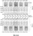
FIG. 11 illustrates reuse of pre-charge equalizer during read operation. - The drawings are only schematic and are non-limiting. In the drawings, the size of some of the elements may be exaggerated and not drawn on scale for illustrative purposes.
- Any reference signs in the claims shall not be construed as limiting the scope.
- In the different drawings, the same reference signs refer to the same or analogous elements.
- The present invention will be described with respect to particular embodiments and with reference to certain drawings but the invention is not limited thereto but only by the claims. The drawings described are only schematic and are non-limiting. In the drawings, the size of some of the elements may be exaggerated and not drawn on scale for illustrative purposes. The dimensions and the relative dimensions do not correspond to actual reductions to practice of the invention.
- Furthermore, the terms first, second and the like in the description and in the claims, are used for distinguishing between similar elements and not necessarily for describing a sequence, either temporally, spatially, in ranking or in any other manner. It is to be understood that the terms so used are interchangeable under appropriate circumstances and that the embodiments of the invention described herein are capable of operation in other sequences than described or illustrated herein.
- Moreover, the terms top, under and the like in the description and the claims are used for descriptive purposes and not necessarily for describing relative positions. It is to be understood that the terms so used are interchangeable under appropriate circumstances and that the embodiments of the invention described herein are capable of operation in other orientations than described or illustrated herein.
- It is to be noticed that the term "comprising", used in the claims, should not be interpreted as being restricted to the means listed thereafter; it does not exclude other elements or steps. It is thus to be interpreted as specifying the presence of the stated features, integers, steps or components as referred to, but does not preclude the presence or addition of one or more other features, integers, steps or components, or groups thereof. Thus, the scope of the expression "a device comprising means A and B" should not be limited to devices consisting only of components A and B. It means that with respect to the present invention, the only relevant components of the device are A and B.
- Reference throughout this specification to "one embodiment" or "an embodiment" means that a particular feature, structure or characteristic described in connection with the embodiment is included in at least one embodiment of the present invention. Thus, appearances of the phrases "in one embodiment" or "in an embodiment" in various places throughout this specification are not necessarily all referring to the same embodiment, but may. Furthermore, the particular features, structures or characteristics may be combined in any suitable manner, as would be apparent to one of ordinary skill in the art from this disclosure, in one or more embodiments.
- Similarly it should be appreciated that in the description of exemplary embodiments of the invention, various features of the invention are sometimes grouped together in a single embodiment, figure, or description thereof for the purpose of streamlining the disclosure and aiding in the understanding of one or more of the various inventive aspects. This method of disclosure, however, is not to be interpreted as reflecting an intention that the claimed invention requires more features than are expressly recited in each claim. Rather, as the following claims reflect, inventive aspects lie in less than all features of a single foregoing disclosed embodiment. Thus, the claims following the detailed description are hereby expressly incorporated into this detailed description, with each claim standing on its own as a separate embodiment of this invention.
- Furthermore, while some embodiments described herein include some but not other features included in other embodiments, combinations of features of different embodiments are meant to be within the scope of the invention, and form different embodiments, as would be understood by those in the art. For example, in the following claims, any of the claimed embodiments can be used in any combination.
- In the description provided herein, numerous specific details are set forth. However, it is understood that embodiments of the invention may be practiced without these specific details. In other instances, well-known methods, structures and techniques have not been shown in detail in order not to obscure an understanding of this description.
- The memory arrangement will be shown, for ease of illustration, as a set of memory elements logically organized in rows and columns. Throughout this description, the terms "horizontal" and "vertical" (related to the terms "row" and "column" respectively) are used to provide a co-ordinate system and for ease of explanation only. They do not need to, but may, refer to an actual physical direction of the device. Furthermore, the terms "column" and "row" are used to describe sets of array elements which are linked together. The linking can be in the form of a Cartesian array of rows and columns; however, the present invention is not limited thereto. As will be understood by those skilled in the art, columns and rows can be easily interchanged and it is intended in this disclosure that these terms be interchangeable. Also, non-Cartesian arrays may be constructed and are included within the scope of the invention. Accordingly the terms "row" and "column" should be interpreted widely. To facilitate in this wide interpretation, the claims refer to logically organised in rows and columns. By this is meant that sets of ... are linked together in a topologically linear intersecting manner; however, that the physical or topographical arrangement need not be so. For example, the rows may be circles and the columns radii of these circles and the circles and radii are described in this invention as "logically organised" rows and columns. Also, specific names of the various lines, e.g. word line and bit line, are intended to be generic names used to facilitate the explanation and to refer to a particular function and this specific choice of words is not intended to in any way limit the invention. It should be understood that all these terms are used only to facilitate a better understanding of the specific structure being described, and are in no way intended to limit the invention.
- In a first aspect, the present invention relates to a memory arrangement for memory cells based on two state resistance change memory elements. Such memory cells typically are arranged in an array structure and comprise crossing word lines and bit lines. For the easy of illustration, the word lines will be shown as horizontally oriented lines and the bit lines will be shown as vertically oriented lines, but as indicated above other orientations are also possible. Each memory cell is connected between a crossing word and bit line. The memory cells are also connected to a source line. Typically, the word line is connected to supply current during read-operation. In some embodiments, the bit line is pre-charged to known supply voltage of VDD before word-line is asserted. In some embodiments, the stored charge over bit-line capacitor is discharged and the current will depend on the state of the memory element (RH or RL) and this current (IH or IL) will flow from the bit-line to the source line. In other embodiment, another known supply voltage I used and the bit line capacitor can be further charged.
- Each bit line comprises a bit line capacitance Cb for storing a charge representative of the state of a selected memory element. In some embodiments, the charge on the bit line capacitance is discharged when current flows from the bit line to the source line or to ground and is influenced by the state, i.e. the resistance, of the memory element. In some embodiments, the charge on the bit line capacitance is charged when current flows from the bit line to the source line. The source line may therefore be connected to a predetermined voltage. It is to be noted that the bit line capacitance remains the same across the array for the same number of cells per column. It is to be noticed that where discharging is mentioned, this does not mean that the charge on the capacitance is fully gone, but that there will be a redistribution of the charge and there will be a residual charge left on the capacitor representative of the state of the memory element.
- The memory cells comprise memory elements being two state resistance change memory element. In such elements, the resistance change is stored as a state. Typically such cells have two possible states, often referred to as a high state and a low state. In the following such states shall, where appropriate, be indicated as RH and RL. It is an advantage of embodiments of the present invention, that systems and devices are provided allowing to provide an accurate reference signal for evaluating whether the memory element is in a high state or in a low state. The more accurate the reference signal is, the more accurate the memory can be read.
- At least two memory cells, being positioned at different bit lines, are defined, e.g. selected, as reference cells. One reference cell thereby is set in a high resistance change mode, while a second reference cell is being set in a low resistance change mode.
- The reference cells correspond with memory cells that are in principle settable to any state, but for the purpose as being used as reference cells these cells are set in advance such that the average charge that will be "sensed" during the pre-charge phase is an average of the high and the low state. If for example two cells are used, typically one cell is set to a high state and one is set to a low state, so that the equalization results in an average of the high and the low state. The memory arrangement thus is put in a particular state prior to the pre-charge.
- According to embodiments of the present invention, at least those bit lines wherein the at least two reference cells are positioned, furthermore are interconnected using an equalizing switch for equalizing a charge on the bit line capacitors of said at least two bit lines, when the reference cells have been read out.
- If QH and QL are the charges defined respectively by IH and IL at the capacitance Cb, then after charge sharing through the equalizing switch, the effective charge on each capacitance becomes "Cbl x Vdd - 0,5 x (QH + QL)", where Vdd is pre-charge voltage.
- The resultant charge of "Cbl x Vdd - 0,5 x (QH + QL)" is used as reference to sense the resistance state of the memory elements in an array. According to embodiments of the present invention, a reference signal thus is generated through at least two, advantageously neighbouring, reference elements, one of them being set having a high resistance RH and one of them being set as having a low resistance state RL. It will be understood that while the example is given for a configuration where discharging of the capacitance is used, the same reasoning will be mutates mutandis applicable when charging of the capacitance is used.
- In order to sense the state of the different other memory elements, a sensing amplifier may be used which makes use of a reference signal being equal to or based on the effective equalized charge.
- The sensing amplifier is thus configured for reading the state of the selected memory element. The bit lines whereon the memory elements are positioned are connectable to the sense amplifier inputs and thus can be connected for sensing the charge for the selected memory element. Combined with the equalized charge from the reference cells, the sensing amplifier provides an output representative of the state of the selected memory element.
- The equalizing switch can for example be designed by a transmission gate, a PFET or an NFET. In advantageous embodiments, the equalizing switch can be an NFET.
- By way of illustration, embodiments of the present invention not being limited thereto, further standard and optional features and advantages of embodiments of the present invention will now further be discussed.
- By way of example, the principle of charge sharing for implementing referencing is illustrated in
FIG. 1. FIG. 1 illustrates part of a memory arrangement. The system illustrates two memory cells positioned on a single word line WL(1) both connected to a bit line BL at a supply voltage V. The two memory cells are selected as reference cells. The cells are set to a high resistance change state and a low resistance change state. In the bit lines a bit line capacitor Cb is present wherein the charge created during pre-charged phase is stored. On the left hand side ofFIG. 1 , the situation is shown wherein no equalizing switch is present. For the cell in the high resistance change state, the resulting current flowing from the bit-line to source line is IH and the corresponding charge discharged from the bit line capacitor in QH, whereas for the cell in the low resistance change state, the resulting current flowing from the bit line to the source line is IL and the corresponding charge discharged from the bit line capacitor is QL. On the right hand side ofFIG. 1 , the situation is shown wherein, according to embodiments of the present invention, an equalizing switch is positioned between the two bit lines wherein the reference cells are positioned. This results in a charge in the bit line capacitors of "Cbl x Vdd - 0,5 x (QH + QL)", which is used by a sensing means, such as for example a sensing amplifier, as a reference signal. -
FIG. 2 illustrates an open bit-line architecture implementation according to an embodiment of the present invention. The memory arrangement comprises an even number of bit lines (columns). A word line WL[0] is fired to read the word in the word line. The state of each individual memory element results in a discharge of a charge from the bit line capacitance. The word from the portion indicated byslice 0, is thus read by asserting WL[0], but in order to appropriately assess, a reference is used generated inslice 1 by asserting the equalizing signal and the reference word line RWL[1] corresponding with a word line wherein reference cells are positioned, with a predetermined memory state. The equalizing signal results in the charge sharing as illustrated inFIG. 1 , such that the resulting reference signal for each of the bit lines is "Cbl x Vdd - 0,5 x (QH + QL)". In the example shown, it is chosen to use all memory elements as reference elements and the date in the reference word line therefore are an equal number (equal to the number of elements to be assessed in the word line of slice 0) of RH and RL state elements are used. The equalizing switch is only shown for the first and second bit line, but typically may be applied to all bit lines. In the example shown, the transistors T1 and T2 are equalizing switches implemented using NFET. If these would be implemented in PFET, then the polarity of the equalizing signal will be active-low. The equalizing signal EQ(1) is thus used to share charge acrossslice 1, in order to average out the effective charge deposited per bit line. The system shown in the example ofFIG. 2 is symmetrical, so if any row is to be read inslice 1, the reference signal can be generated inslice 0. It is to be noticed that the invention is not limited thereto and that also an asymmetric arrangement can be used, whereby there are only memory elements that are not reference elements in one of the slices and whereby the other slice is purely used as reference signal generating element. It is to be noticed that according to embodiments of the present invention, any row in the array can be used as reference word line RWL. The memory arrangement may for example comprise a memory controller for assigning a reference row dynamically during the life of the memory. - In embodiments of the present invention, analysis of the content of a memory cell is performed in a sensing means, e.g. a sensing amplifier. For the sake of completeness, one example of a sensing amplifier is shown in
FIG. 3 , but any sensing means allowing to evaluate a signal as function of a reference signal may be used. - Still referring to
FIG. 2 , the charge averaging principle applied to a 32 bit arrangement will be discussed below. If for example there are 32 bits in a word for an open-bit-line architecture as shown inFIG. 2 , the situation can be as follows : If all reference cell states exactly match then the effective charge on a 32 bit-line can be calculates as "32 x [Cbl x Vdd - 0,5 x (QH + QL)]", which results in a charge per bit-line as "32 x [Cbl x Vdd - 0,5 x (QH + QL)]/32". Note that in this case the averaging is done over all bit lines, so according to embodiments the charge is equalized over at least two cells, but may be equalized over more than two cells. Advantageously this may be done in couples of cells in a high and a low resistance state, but it could alternatively even be done for reference cells whereby a different number of reference cells with a high resistance state compared to a low resistance state is used, provided the equalizing compensates for such different numbers. Further to the the 32 bit-line example, if there is a mismatch in one of the reference cells, for example if one of the reference cell resistances has changed from RH to (RH+ΔRH), this results in charge change written as (QH-ΔQH). Upon equalization total charge on 32 bit-lines

- This result in average charge change per cell as CblVdd -[0.5×(QH+QL) -ΔQH/32]. The effective error in charge per bit-line will be ±ΔQHL/N where N is number of reference cells in a ROW and ±ΔQHL represents difference in charge deposited due to change in a state resistance of individual reference cell. The error thus is reduced by a factor equal to the number of reference cells used.
- It is an advantage of embodiments of the present invention that the memory arrangement follows a simple design and does not require analog referencing. This avoids the need for input output transistors and higher supplies. Moreover the referencing system/method is simplified. Since the references are averaged, the accuracy is increased. It is to be noted that at pitch sense - amplifiers without multiplexing are possible, comparable to the situation with DRAM. The specific arrangement requires double access power, which is not the case for some embodiments described below.
- In
FIG. 4 one example of an implementation is shown wherein multiplexing is used. The latter is advantageous since it allows to use a single sensing means for the different bit lines to be read out. The memory arrangement shown is similar to the arrangement shown inFIG. 2 , except in that the different sensing amplifiers are replaced by a single sensing amplifier that is connected to the different bit lines of the memory cells to be read out and the reference memory cells by multiplexers. The implementation shown requires that there are two multiplexers. - In the arrangement shown in
FIG. 4 , for a time Δt time all bit-lines in slice-1 are dis-charged and equalized, thus generating a reference signal. Before enabling the multiplexer, all equalizers are switched off along with the word-line to isolate respective charge per reference bit-line. The reference charge is shared with a sensing means, e.g. with the sense-amplifier internal nodes IO/IOB illustrated inFIG. 3 , by enabling EMUX[1], which ensures true sensing of single bit-line. The corresponding signals for the different lines are also shown inFIG. 4 . In the upper slide, the source line, and the word line WL[0] are driven for selecting the cell to be sensed during a time Δt. The equalizing signal EQ[0] inslice 0 is not applied, since no reference signals are to be measured in slice 0 (the reference measurements are made in slice 1). Inslice 1, the reference word line WL[1], also referred to as WLR[1], and the equalizing signal is driven during a time Δt so as to share charge over the reference elements. Thereafter, during a time Δt1, the charge is shared between the nodes of the sensing means and the reference bit line, so as to provide the sensing means with an appropriate reference signal. Following thereon, the sensing means senses the state of the memory element of interest inslice 0. - In an alternative embodiment, a closed bit line multiplexing implementation is described. An example thereof is shown in
FIG. 5 . The memory arrangement is adapted for sensing, whereby two sub-arrangements of memory elements are provided arranged such that each sub-arrangement has different bit lines, but that these share the word lines. Each sub-arrangement has a separate multiplexer and in each of these sub arrangements memory elements to be sensed and reference memory elements are present. In the embodiment shown, the reference is generated out of two reference column cells for sensing two bits. Each of the reference column (bit line wherein the reference element is positioned), belongs to a different sub-arrangement, but the reference columns share charge using an equalizing switch. In the present embodiment, effective power is reduced since the reference word line RWL is not required to generate the reference charge (the reference elements are positioned on the word line where also memory cells to be measured are positioned. The two reference bit lines RBL[0] and RBL[1] are the reference bit-lines used for generating a reference per multiplexer, The averaging of charge can be achieved by adding equalizer transistors between the two reference bit-lines RBL (or if more reference bit lines are used between all reference bit-lines RBL). In operation, the word line is fired for a period in time resulting in charge generation, both for memory cells to be read as for reference cells. At the same time the equalizing switch is operated so that charge sharing occurs for the bit lines of the reference cells. Thereafter, the sensing means is initiated, allowing sensing of the memory cells to be evaluated as function of the reference signal. Since no separate cycle is required for sharing the charge in the reference cells because it can be done while the word line is fired, this results in a fast system, compared to the system shown inFIG. 4 . - Further by way of illustration, an alternative (compared to
FIG. 1 ) memory arrangement is shown inFIG. 6 , wherein precharging via the source line is performed. The latter is obtained by implementing a voltage per bit line instead of applying a sensing current. Precharging can be performed using a voltage Vdd, resulting in an additional charge Cs*Vdd being present on the capacitor. It is to be noticed that the initial charge may correspond with the initial charge Cs*Vdd to maximize the range to Vdd or Vss, but can be different. The resulting charge then is a combination of the source line discharge from VDD and the charge induced by the resistance of the reference elements, resulting in
- In yet another arrangement, as shown in
FIG. 7 , a charging of the bitline from source line is performed. The resulting charge then is the charge deposited by the resistance of the reference elements, resulting in
- By way of illustration, embodiments of the present invention not being limited thereto, the averaging effect of the equalizer has been studied in some more detail.
- In the study, a same number of RH and RL state STT-MRAM cells was used in the reference memory elements. It was seen that a 14% reduction in RH sensing spread was obtained and a 17% reduction in RL sensing spread when 4 pairs are averaged in comparison with 1 pair. Averaging all reference cells improves the spread of the reference and in effect improves the yield. It was also noted that the reference generation according to embodiments of the present invention averages out local variations.
- In a second aspect, the present invention relates to a method for sensing a state of a two state resistance change memory element. The method may be advantageously implemented for a memory arrangement as described above. The method comprises selecting at least two reference cells positioned at different bit lines, whereby one reference cell has a high resistance change state and a second reference cell has a low resistance change state, and equalizing, over the bit lines, a charge caused by the selection of said two reference cells so as to obtain an equalized charge that can be used as a reference. The method also comprises selecting a memory element for which a state is to be sensed, thereby generating a sensing charge in the bit line and evaluating said sensing charge as function of said reference equalized charge so as to derive a state of said tow state resistance change memory element. The selection of at least two reference cells may be a selection of previously determined reference cells but also may encompass dynamical selection of reference cells (or even a reference word). Such dynamic selection may be such that it corresponds with positioning a reference cell at a position of a memory element having a stuck at 0/1 error. Further features and advantages may correspond with the functionality of the components as described in the first aspect.
- According to some embodiments of the present invention, the above described system and method also may be used for optimizing the yield of a memory arrangement. At present, often redundancy is used to guarantee a sufficient yield. The ideas described above could nevertheless be used to cope with stuck at 0/1 faults in memory elements. More particularly, by dynamically altering the reference cells used in the memory arrangement towards memory cells where a stuck at 0/1 fault occurs, the previously used reference cells could be used for storage and the memory cells comprising the faults could be used as a reference cell, since for reference cells a fixed resistance value is required. In other words, memory cells with a stuck at 0/1 fault can be reused and the failure can be rectified. The memory arrangement may have a memory controller programmed for altering one or more reference memory elements.
- The principle is described with reference to
FIG. 8 , illustrating a memory arrangement wherein a Mux-4 multiplexer is used for multiplexing Bit-lines B[0,11]. The multiplexer allows to select one bit line potential and transfers it on the data line or reference data line based on the multiplexing. For example, suppose that the 4th word in a word line (ROW) is used for generating a reference for other words in a ROW by using the charge sharing concept as described above. The equalizer transistor then is set to equalize charges on BL[3], BL[7],BL[11] and BL[15] for a 4 bit word in a memory array. For the selected word line (ROW), the equalizer transistor EQ[3] signal equalizes and generates the reference and then transfers the equalized charge on a reference data line through the TGR4 (transmission gate/nmos/pmos) selector. The reference data line DL1 is a sense node of an amplifier. The xdec[0:3] signals are used to select the TG* transmission gates to transfer charges from BL to DLB1 node of an amplifier. As the 4th word is used for referencing, xdec[3] selects the reference signal which will result into invalid read for memory. Similarly, any word in a ROW can be used for reference where word used for reference can be changed by asserting EQ[*] signal. During the life span of the memory, if suppose memory stuck at high or low resistance state in a ROW then memory controller goes into debug mode to detect a failed location of memory element by regenerating reference from other words and generating a reference from word consisting of stuck at memory element by updating data into it. - A schematic representation of a memory controller is shown in
FIG. 9 . It indicates the memory controller as well as the memory elements, referred to as memory. Furthermore it indicates typical signal exchange performed by the controller. The controller may send address data, CLK data and control data to the memory, as well as interchange other data in/out with the memory. The controller may operate based on a predetermined algorithm, a neural network, etc. The controller may be programmed for, if a read failure is encountered for a word, entering into a debug mode to detect the failure. Upon detection of the failure, in some embodiments the controller may decide to set or reset reference memory elements, e.g. a reference word used in a row (on a Word Line). Communication between the memory and the memory controller may be performed using a handshake. Such a handshake between the memory and the memory controller may be as indicated inFIG. 9 , illustrating the type of data that is sent or interchanged. The memory controller may act as a master that decides or sets reference memory elements, such as reference words, for a row. - By way of illustration, embodiments of the present invention not being limited thereto, an example of an algorithm used in detecting failure in the data of a row or reference row is shown in
FIG. 10 . - In a first step, a read failure is detected by the microcontroller. This triggers the microcontroller to go into debug mode.
- If the memory controller is able to read other words in the row, it is decided that the reference word is intact. Then (1111) and (0000) data is written to the data word and read. The data is compared and the result is stored. Based on the information obtained an error bit is reported. If the error is a stuck at 0/1 error, the algorithm proceeds by writing (0101/1010/0110/1001) to the data word to include the stuck at 0/1 error. The data word is then changed as reference word in the row. The memory controller thereafter exits the debug mode.
- If upon entry into the debug mode, the other words in the word row cannot be read, the 0th reference is incorrect and the reference word in the row is changed. The data (0101/1010/0110/1001) is written to the new 0th reference word. Then (1111) and (0000) data is written to the reference word and read. The data is compared and the result is stored. Based on the information obtained an error bit is reported. If the error is a stuck at 0/1 error, the algorithm proceeds by writing (0101/1010/0110/1001) to the reference word to include the stuck at 0/1 error. Thereafter, the system exits the debug mode.
- It is to be noted that the same concept can be used to detect short and open circuit. For example, if one of the memory elements is shortened, this will increase a charge over the sense node more than is either charge deposited by the high resistance change state or low resistance change state. This will result in all 0 or 1 states as read output. In other words, shortened memory elements can be detected. Similarly, an open circuit will result in no charge being deposited over the sense node, resulting in a lower charge than RH or RL state element and thus will result in all 1 or 0 as read out based on the design.
- In yet a further aspect, the present invention relates to a memory controller for controlling a memory according to a method as described in the second aspect. The memory controller may be implemented in software as well as in hardware. The above described method embodiments as well as the memory controller may be implemented as software in a processor. One configuration of such a processor may for example include at least one programmable computing component coupled to a memory subsystem that includes at least one form of memory, e.g., RAM, ROM, and so forth. It is to be noted that the computing component or computing components may be a general purpose, or a special purpose computing component, and may be for inclusion in a device, e.g., a chip that has other components that perform other functions. Thus, one or more aspects of the present invention can be implemented in digital electronic circuitry, or in computer hardware, firmware, software, or in combinations of them. For example, each of the method steps of the method for controlling the memory may be a computer implemented step implemented as one or a set of instructions. Thus, while a processor as such is prior art, a system that includes the instructions for controlling the memory is not prior art.
- The present invention thus also includes a computer program product which provides the functionality of any of the methods according to the present invention when executed on a computing device. Vice versa, the computer program products described above may be implemented as hardware in computing devices. Alternatively, the computer program products may be implemented as computer-implemented methods and the present invention therefore also relates to the corresponding computer-implemented methods.
- In another aspect, the present invention relates to a data carrier for carrying a computer program product as described above. Such a data carrier may comprise a computer program product tangibly embodied thereon and may carry machine-readable code for execution by a programmable processor. The present invention thus relates to a carrier medium carrying a computer program product that, when executed on computing means, provides instructions for executing any of the methods as described above. The term "carrier medium" refers to any medium that participates in providing instructions to a processor for execution. Such a medium may take many forms, including but not limited to, non-volatile media, and transmission media. Non-volatile media includes, for example, optical or magnetic disks, such as a storage device which is part of mass storage. Common forms of computer readable media include, a CD-ROM, a DVD, a flexible disk or floppy disk, a tape, a memory chip or cartridge or any other medium from which a computer can read. Various forms of computer readable media may be involved in carrying one or more sequences of one or more instructions to a processor for execution. The computer program product can also be transmitted via a carrier wave in a network, such as a LAN, a WAN or the Internet. Transmission media can take the form of acoustic or light waves, such as those generated during radio wave and infrared data communications. Transmission media include coaxial cables, copper wire and fibre optics, including the wires that comprise a bus within a computer.
Claims (15)
- A memory arrangement comprising a plurality of memory cells arranged in an array structure, wherein each memory cell comprises a memory element being a two state resistance change memory element,
the memory arrangement comprising crossing word and bit lines and each memory cell is being connected between a different crossing of a word line and a bit line, the memory cells furthermore being connectable to a source line,
each bit line has a bit line capacitance, for storing a charge representative of the state of a selected memory element,
at least two memory cells, positioned at different bit lines but on a same word line, are being defined as reference cells, one reference cell being set in a high resistance state and a second reference cell being in a low resistance state,
at least those bit lines wherein the reference cells are defined furthermore are interconnected by an equalizing switch, for equalizing the charges on the bit line capacitors of said at least two bit lines. - A memory arrangement according to claim 1, wherein the charge representative of the state of a selected memory element is defined when current is running through the selected memory element.
- A memory arrangement according to claim 1, wherein the memory arrangement furthermore comprises a sense amplifier for reading the state of a selected memory element, different from the cells defined as reference cells, said sense amplifier being configured for using the equalized charge on the bit line capacitors as a reference signal and further configured for using the charge of the selected memory element for reading the state.
- A memory arrangement according to any of the previous claims, wherein the equalizing switch comprises a Field Effect Transistor (FET) and/or wherein the memory elements are STT-MRAM memory elements or RRAM memory elements.
- A memory arrangement according to any of the previous claims, wherein the memory elements are connected to the source line using a selection switch for selectively contacting the memory elements with the supply line during a pre-charge phase thereof.
- A memory arrangement according to any of the previous claims, wherein the memory arrangement comprises a memory controller for dynamically selecting the reference cells used.
- A memory arrangement according to any of the previous claims, wherein the equalizing switches are positioned between more than those bit lines comprising the reference cells, and wherein the reference cells can be selected to be cells in those bit lines interconnected via equalizing switches.
- A memory arrangement according to any of the previous claims, wherein the memory arrangement comprises reference cells in each of the bit lines, whereby each of the bit lines is interconnected by an equalizing switches to another bit line.
- A memory arrangement according to any of the previous claims in as far as dependent on claim 3, wherein the memory arrangement comprises a first sub-arrangement and a second sub-arrangement,
each of said sub-arrangements- being connected to the sense amplifier through a multiplexer,- comprising distinct word lines and- comprising a same number of bit lines,wherein the reference cells are all defined/positioned in one sub-arrangement selected by a given Word line, and the selected memory element is in the other sub-arrangement. - A memory arrangement according to any of claims 2 to 8, wherein the memory arrangement comprises at least a first and a second sub-arrangement, each sub-arrangement- being connected to a sense amplifier through a multiplexer,- sharing word lines with another sub-arrangementwherein the reference elements are positioned in two bit lines, each bit line belonging to a different sub-arrangement and wherein the reference signal is generated based on an equalized charge in said two bit lines being positioned in the different sub-arrangements, and the selected memory element is located in each subarray and connected to a bit line different from the reference elements.
- A memory arrangement according to any of the previous claims, wherein the memory arrangement furthermore comprises a memory controller for detecting a stuck at 0/1 error in a memory cell, the controller further reserving the stuck at 0/1 memory cell for reference cell purpose (only) and for altering the state of the non stuck at 0/1 reference cells so as to include the state of the memory cell comprising the stuck at 0/1 error.
- A memory arrangement according to any of the previous claims, wherein a multiplexer is used for multiplexing memory elements along bit lines of the memory arrangement, whereby the multiplexer is arranged for selecting a bit line potential of the selected memory element and transferring a corresponding charge to the sense amplifier and/or wherein a multiplexer is used for multiplexing memory elements along bit lines of the memory arrangement, whereby the multiplexer is arranged for selecting a bit line potential of the reference signal and transferring a corresponding charge to the sense amplifier.
- A memory arrangement according to claim 12, wherein the memory arrangement is adapted for using an n-bit word in memory cells along a word line as reference, and wherein the system comprises a memory controller for dynamically altering the n-bit word used as reference, and/or wherein the bit line potential is transferred by a transfer switch to the sense amplifier, the transfer switches, the selection switches, the switches in the multiplexer and/or the equalizing switches being any of a transmission gate, a PFET or an NFET.
- A method for sensing a state of a two state resistance change memory element in a memory arrangement according to any of claims 1 to 13, the method comprising- Selecting at least two reference cells positioned at different bit lines but on the same word line, whereby one reference cell has a high resistance state and a second reference cell having a low resistance change state,- Equalizing a charge of the at least two reference cells, so as to obtain an equalized charge that can be used as a reference,- Selecting the two state resistance change memory element in the memory arrangement for which a state is to be sensed, thereby generating a sensing charge, and- Evaluating said sensing charge in a sensing amplifier, as function of said reference equalized charge so as to derive a signal representative of a state of the two state resistance change memory element.
- Use of a memory arrangement according to any of claims 1 to 13, for storing and/or reading out data stored in the memory arrangement.
Applications Claiming Priority (1)
| Application Number | Priority Date | Filing Date | Title |
|---|---|---|---|
| EP16160785 | 2016-03-16 |
Publications (2)
| Publication Number | Publication Date |
|---|---|
| EP3220391A1 true EP3220391A1 (en) | 2017-09-20 |
| EP3220391B1 EP3220391B1 (en) | 2020-02-19 |
Family
ID=55628756
Family Applications (1)
| Application Number | Title | Priority Date | Filing Date |
|---|---|---|---|
| EP17161286.4A Active EP3220391B1 (en) | 2016-03-16 | 2017-03-16 | Reference generation for high density two state resistance change memories |
Country Status (3)
| Country | Link |
|---|---|
| US (1) | US10170182B2 (en) |
| EP (1) | EP3220391B1 (en) |
| KR (1) | KR101920993B1 (en) |
Families Citing this family (5)
| Publication number | Priority date | Publication date | Assignee | Title |
|---|---|---|---|---|
| US10515679B2 (en) | 2018-02-06 | 2019-12-24 | Globalfoundries Inc. | Magneto-resistive memory structures with improved sensing, and associated sensing methods |
| KR102870853B1 (en) | 2019-04-29 | 2025-10-13 | 삼성전자주식회사 | Memory controller, memory system having the same and operating method of memory controller |
| US11450357B2 (en) * | 2019-10-30 | 2022-09-20 | Taiwan Semiconductor Manufacturing Co., Ltd. | Structure for multiple sense amplifiers of memory device |
| DE102020120890A1 (en) | 2019-10-30 | 2021-05-06 | Taiwan Semiconductor Manufacturing Co., Ltd. | STRUCTURE FOR MULTIPLE READING AMPLIFIERS OF A STORAGE DEVICE |
| US12124942B2 (en) * | 2019-12-03 | 2024-10-22 | Anaflash Inc. | Serialized neural network computing unit |
Citations (2)
| Publication number | Priority date | Publication date | Assignee | Title |
|---|---|---|---|---|
| US20020080644A1 (en) * | 2000-12-26 | 2002-06-27 | Kabushiki Kaisha Toshiba | Magnetic random access memory |
| US20150262622A1 (en) * | 2014-03-13 | 2015-09-17 | Kabushiki Kaisha Toshiba | Resistance change memory |
Family Cites Families (15)
| Publication number | Priority date | Publication date | Assignee | Title |
|---|---|---|---|---|
| JP3218844B2 (en) * | 1994-03-22 | 2001-10-15 | 松下電器産業株式会社 | Semiconductor memory device |
| JP2004022073A (en) * | 2002-06-17 | 2004-01-22 | Elpida Memory Inc | Semiconductor storage device |
| US6600690B1 (en) * | 2002-06-28 | 2003-07-29 | Motorola, Inc. | Sense amplifier for a memory having at least two distinct resistance states |
| JP3962048B2 (en) | 2004-09-28 | 2007-08-22 | 株式会社東芝 | Semiconductor memory |
| KR100735750B1 (en) | 2005-12-15 | 2007-07-06 | 삼성전자주식회사 | Semiconductor devices having reference cell blocks and sense amplifier units for generating a plurality of uniform reference data and systems for adopting the same |
| US7342819B2 (en) * | 2006-03-03 | 2008-03-11 | Infineon Technologies Ag | Methods for generating a reference voltage and for reading a memory cell and circuit configurations implementing the methods |
| JP5076361B2 (en) * | 2006-05-18 | 2012-11-21 | 株式会社日立製作所 | Semiconductor device |
| JP2010182353A (en) * | 2009-02-04 | 2010-08-19 | Elpida Memory Inc | Semiconductor memory device and reading method therefor |
| EP2309514B1 (en) * | 2009-10-05 | 2016-01-06 | Crocus Technology | Circuit for generating adjustable timing signals for sensing a self-referenced MRAM cell |
| JP5614150B2 (en) | 2010-07-29 | 2014-10-29 | ソニー株式会社 | Resistance change memory device |
| US8570812B2 (en) * | 2011-08-23 | 2013-10-29 | Texas Instruments Incorporated | Method of reading a ferroelectric memory cell |
| US8498169B2 (en) | 2011-09-02 | 2013-07-30 | Qualcomm Incorporated | Code-based differential charging of bit lines of a sense amplifier |
| US9390779B2 (en) | 2013-03-15 | 2016-07-12 | Qualcomm Incorporated | System and method of sensing a memory cell |
| JP5480420B1 (en) * | 2013-03-26 | 2014-04-23 | 株式会社東芝 | Magnetic memory |
| WO2015085093A1 (en) * | 2013-12-06 | 2015-06-11 | Rambus Inc. | 2t-1r architecture for resistive ram |
-
2017
- 2017-03-14 US US15/458,874 patent/US10170182B2/en active Active
- 2017-03-15 KR KR1020170032292A patent/KR101920993B1/en active Active
- 2017-03-16 EP EP17161286.4A patent/EP3220391B1/en active Active
Patent Citations (2)
| Publication number | Priority date | Publication date | Assignee | Title |
|---|---|---|---|---|
| US20020080644A1 (en) * | 2000-12-26 | 2002-06-27 | Kabushiki Kaisha Toshiba | Magnetic random access memory |
| US20150262622A1 (en) * | 2014-03-13 | 2015-09-17 | Kabushiki Kaisha Toshiba | Resistance change memory |
Also Published As
| Publication number | Publication date |
|---|---|
| KR101920993B1 (en) | 2019-02-13 |
| KR20170107918A (en) | 2017-09-26 |
| US10170182B2 (en) | 2019-01-01 |
| EP3220391B1 (en) | 2020-02-19 |
| US20170271002A1 (en) | 2017-09-21 |
Similar Documents
| Publication | Publication Date | Title |
|---|---|---|
| US10170182B2 (en) | Resistance change memory device configured for state evaluation based on reference cells | |
| JP5502692B2 (en) | Circuit for generating an adjustable timing signal for sensing a self-referencing MRAM cell | |
| US6650584B2 (en) | Full stress open digit line memory device | |
| JP2673395B2 (en) | Semiconductor memory device and test method thereof | |
| US8891313B2 (en) | Memory device and read operation method thereof | |
| US10170161B2 (en) | Semiconductor memory device and test method therefor | |
| JP5651292B2 (en) | Semiconductor memory device and test method thereof | |
| CN100501876C (en) | Memory and method for soft defect detection in a memory | |
| US9589608B2 (en) | Semiconductor memory device | |
| EP0766258B1 (en) | Dram signal margin test method | |
| KR100796050B1 (en) | Semiconductor memory device and multiplexer control method | |
| JPH08195100A (en) | Semiconductor memory device operation test method and semiconductor memory device | |
| EP0766259B1 (en) | Dynamic random access memory | |
| US20070076462A1 (en) | Semiconductor memory and method for operating a semiconductor memory comprising a plurality of memory cells | |
| JP4874637B2 (en) | Nonvolatile memory device and reading method thereof | |
| US7457143B2 (en) | Memory device with shared reference and method | |
| JP2012099202A (en) | Semiconductor device | |
| US6950353B1 (en) | Cell data margin test with dummy cell | |
| JP4184036B2 (en) | Semiconductor memory device and test method thereof | |
| US9530463B1 (en) | Memory device and method thereof | |
| JP2012009100A (en) | Nonvolatile storage device | |
| US8767493B2 (en) | SRAM differential voltage sensing apparatus | |
| US20150213883A1 (en) | Testing signal development on a bit line in an sram | |
| US7474573B2 (en) | Semiconductor memory device capable of writing different data in cells coupled to one word line during burn-in test | |
| US7511987B2 (en) | Memory device with hierarchy bit line |
Legal Events
| Date | Code | Title | Description |
|---|---|---|---|
| PUAI | Public reference made under article 153(3) epc to a published international application that has entered the european phase |
Free format text: ORIGINAL CODE: 0009012 |
|
| STAA | Information on the status of an ep patent application or granted ep patent |
Free format text: STATUS: THE APPLICATION HAS BEEN PUBLISHED |
|
| AK | Designated contracting states |
Kind code of ref document: A1 Designated state(s): AL AT BE BG CH CY CZ DE DK EE ES FI FR GB GR HR HU IE IS IT LI LT LU LV MC MK MT NL NO PL PT RO RS SE SI SK SM TR |
|
| AX | Request for extension of the european patent |
Extension state: BA ME |
|
| STAA | Information on the status of an ep patent application or granted ep patent |
Free format text: STATUS: REQUEST FOR EXAMINATION WAS MADE |
|
| 17P | Request for examination filed |
Effective date: 20180320 |
|
| RBV | Designated contracting states (corrected) |
Designated state(s): AL AT BE BG CH CY CZ DE DK EE ES FI FR GB GR HR HU IE IS IT LI LT LU LV MC MK MT NL NO PL PT RO RS SE SI SK SM TR |
|
| GRAP | Despatch of communication of intention to grant a patent |
Free format text: ORIGINAL CODE: EPIDOSNIGR1 |
|
| STAA | Information on the status of an ep patent application or granted ep patent |
Free format text: STATUS: GRANT OF PATENT IS INTENDED |
|
| INTG | Intention to grant announced |
Effective date: 20191011 |
|
| GRAS | Grant fee paid |
Free format text: ORIGINAL CODE: EPIDOSNIGR3 |
|
| GRAA | (expected) grant |
Free format text: ORIGINAL CODE: 0009210 |
|
| STAA | Information on the status of an ep patent application or granted ep patent |
Free format text: STATUS: THE PATENT HAS BEEN GRANTED |
|
| AK | Designated contracting states |
Kind code of ref document: B1 Designated state(s): AL AT BE BG CH CY CZ DE DK EE ES FI FR GB GR HR HU IE IS IT LI LT LU LV MC MK MT NL NO PL PT RO RS SE SI SK SM TR |
|
| REG | Reference to a national code |
Ref country code: CH Ref legal event code: EP |
|
| REG | Reference to a national code |
Ref country code: DE Ref legal event code: R096 Ref document number: 602017011822 Country of ref document: DE |
|
| REG | Reference to a national code |
Ref country code: AT Ref legal event code: REF Ref document number: 1235878 Country of ref document: AT Kind code of ref document: T Effective date: 20200315 |
|
| REG | Reference to a national code |
Ref country code: IE Ref legal event code: FG4D |
|
| REG | Reference to a national code |
Ref country code: NL Ref legal event code: MP Effective date: 20200219 |
|
| PG25 | Lapsed in a contracting state [announced via postgrant information from national office to epo] |
Ref country code: NO Free format text: LAPSE BECAUSE OF FAILURE TO SUBMIT A TRANSLATION OF THE DESCRIPTION OR TO PAY THE FEE WITHIN THE PRESCRIBED TIME-LIMIT Effective date: 20200519 Ref country code: RS Free format text: LAPSE BECAUSE OF FAILURE TO SUBMIT A TRANSLATION OF THE DESCRIPTION OR TO PAY THE FEE WITHIN THE PRESCRIBED TIME-LIMIT Effective date: 20200219 Ref country code: FI Free format text: LAPSE BECAUSE OF FAILURE TO SUBMIT A TRANSLATION OF THE DESCRIPTION OR TO PAY THE FEE WITHIN THE PRESCRIBED TIME-LIMIT Effective date: 20200219 |
|
| REG | Reference to a national code |
Ref country code: LT Ref legal event code: MG4D |
|
| PG25 | Lapsed in a contracting state [announced via postgrant information from national office to epo] |
Ref country code: IS Free format text: LAPSE BECAUSE OF FAILURE TO SUBMIT A TRANSLATION OF THE DESCRIPTION OR TO PAY THE FEE WITHIN THE PRESCRIBED TIME-LIMIT Effective date: 20200619 Ref country code: HR Free format text: LAPSE BECAUSE OF FAILURE TO SUBMIT A TRANSLATION OF THE DESCRIPTION OR TO PAY THE FEE WITHIN THE PRESCRIBED TIME-LIMIT Effective date: 20200219 Ref country code: SE Free format text: LAPSE BECAUSE OF FAILURE TO SUBMIT A TRANSLATION OF THE DESCRIPTION OR TO PAY THE FEE WITHIN THE PRESCRIBED TIME-LIMIT Effective date: 20200219 Ref country code: LV Free format text: LAPSE BECAUSE OF FAILURE TO SUBMIT A TRANSLATION OF THE DESCRIPTION OR TO PAY THE FEE WITHIN THE PRESCRIBED TIME-LIMIT Effective date: 20200219 Ref country code: GR Free format text: LAPSE BECAUSE OF FAILURE TO SUBMIT A TRANSLATION OF THE DESCRIPTION OR TO PAY THE FEE WITHIN THE PRESCRIBED TIME-LIMIT Effective date: 20200520 Ref country code: BG Free format text: LAPSE BECAUSE OF FAILURE TO SUBMIT A TRANSLATION OF THE DESCRIPTION OR TO PAY THE FEE WITHIN THE PRESCRIBED TIME-LIMIT Effective date: 20200519 |
|
| PG25 | Lapsed in a contracting state [announced via postgrant information from national office to epo] |
Ref country code: NL Free format text: LAPSE BECAUSE OF FAILURE TO SUBMIT A TRANSLATION OF THE DESCRIPTION OR TO PAY THE FEE WITHIN THE PRESCRIBED TIME-LIMIT Effective date: 20200219 |
|
| PG25 | Lapsed in a contracting state [announced via postgrant information from national office to epo] |
Ref country code: LT Free format text: LAPSE BECAUSE OF FAILURE TO SUBMIT A TRANSLATION OF THE DESCRIPTION OR TO PAY THE FEE WITHIN THE PRESCRIBED TIME-LIMIT Effective date: 20200219 Ref country code: CZ Free format text: LAPSE BECAUSE OF FAILURE TO SUBMIT A TRANSLATION OF THE DESCRIPTION OR TO PAY THE FEE WITHIN THE PRESCRIBED TIME-LIMIT Effective date: 20200219 Ref country code: ES Free format text: LAPSE BECAUSE OF FAILURE TO SUBMIT A TRANSLATION OF THE DESCRIPTION OR TO PAY THE FEE WITHIN THE PRESCRIBED TIME-LIMIT Effective date: 20200219 Ref country code: SK Free format text: LAPSE BECAUSE OF FAILURE TO SUBMIT A TRANSLATION OF THE DESCRIPTION OR TO PAY THE FEE WITHIN THE PRESCRIBED TIME-LIMIT Effective date: 20200219 Ref country code: PT Free format text: LAPSE BECAUSE OF FAILURE TO SUBMIT A TRANSLATION OF THE DESCRIPTION OR TO PAY THE FEE WITHIN THE PRESCRIBED TIME-LIMIT Effective date: 20200712 Ref country code: RO Free format text: LAPSE BECAUSE OF FAILURE TO SUBMIT A TRANSLATION OF THE DESCRIPTION OR TO PAY THE FEE WITHIN THE PRESCRIBED TIME-LIMIT Effective date: 20200219 Ref country code: SM Free format text: LAPSE BECAUSE OF FAILURE TO SUBMIT A TRANSLATION OF THE DESCRIPTION OR TO PAY THE FEE WITHIN THE PRESCRIBED TIME-LIMIT Effective date: 20200219 Ref country code: EE Free format text: LAPSE BECAUSE OF FAILURE TO SUBMIT A TRANSLATION OF THE DESCRIPTION OR TO PAY THE FEE WITHIN THE PRESCRIBED TIME-LIMIT Effective date: 20200219 Ref country code: DK Free format text: LAPSE BECAUSE OF FAILURE TO SUBMIT A TRANSLATION OF THE DESCRIPTION OR TO PAY THE FEE WITHIN THE PRESCRIBED TIME-LIMIT Effective date: 20200219 |
|
| REG | Reference to a national code |
Ref country code: CH Ref legal event code: PL |
|
| REG | Reference to a national code |
Ref country code: AT Ref legal event code: MK05 Ref document number: 1235878 Country of ref document: AT Kind code of ref document: T Effective date: 20200219 |
|
| REG | Reference to a national code |
Ref country code: DE Ref legal event code: R097 Ref document number: 602017011822 Country of ref document: DE |
|
| PG25 | Lapsed in a contracting state [announced via postgrant information from national office to epo] |
Ref country code: MC Free format text: LAPSE BECAUSE OF FAILURE TO SUBMIT A TRANSLATION OF THE DESCRIPTION OR TO PAY THE FEE WITHIN THE PRESCRIBED TIME-LIMIT Effective date: 20200219 |
|
| REG | Reference to a national code |
Ref country code: BE Ref legal event code: MM Effective date: 20200331 |
|
| PLBE | No opposition filed within time limit |
Free format text: ORIGINAL CODE: 0009261 |
|
| STAA | Information on the status of an ep patent application or granted ep patent |
Free format text: STATUS: NO OPPOSITION FILED WITHIN TIME LIMIT |
|
| PG25 | Lapsed in a contracting state [announced via postgrant information from national office to epo] |
Ref country code: LU Free format text: LAPSE BECAUSE OF NON-PAYMENT OF DUE FEES Effective date: 20200316 |
|
| 26N | No opposition filed |
Effective date: 20201120 |
|
| PG25 | Lapsed in a contracting state [announced via postgrant information from national office to epo] |
Ref country code: IT Free format text: LAPSE BECAUSE OF FAILURE TO SUBMIT A TRANSLATION OF THE DESCRIPTION OR TO PAY THE FEE WITHIN THE PRESCRIBED TIME-LIMIT Effective date: 20200219 Ref country code: LI Free format text: LAPSE BECAUSE OF NON-PAYMENT OF DUE FEES Effective date: 20200331 Ref country code: CH Free format text: LAPSE BECAUSE OF NON-PAYMENT OF DUE FEES Effective date: 20200331 Ref country code: IE Free format text: LAPSE BECAUSE OF NON-PAYMENT OF DUE FEES Effective date: 20200316 Ref country code: AT Free format text: LAPSE BECAUSE OF FAILURE TO SUBMIT A TRANSLATION OF THE DESCRIPTION OR TO PAY THE FEE WITHIN THE PRESCRIBED TIME-LIMIT Effective date: 20200219 |
|
| PG25 | Lapsed in a contracting state [announced via postgrant information from national office to epo] |
Ref country code: BE Free format text: LAPSE BECAUSE OF NON-PAYMENT OF DUE FEES Effective date: 20200331 Ref country code: SI Free format text: LAPSE BECAUSE OF FAILURE TO SUBMIT A TRANSLATION OF THE DESCRIPTION OR TO PAY THE FEE WITHIN THE PRESCRIBED TIME-LIMIT Effective date: 20200219 Ref country code: PL Free format text: LAPSE BECAUSE OF FAILURE TO SUBMIT A TRANSLATION OF THE DESCRIPTION OR TO PAY THE FEE WITHIN THE PRESCRIBED TIME-LIMIT Effective date: 20200219 |
|
| GBPC | Gb: european patent ceased through non-payment of renewal fee |
Effective date: 20210316 |
|
| PG25 | Lapsed in a contracting state [announced via postgrant information from national office to epo] |
Ref country code: GB Free format text: LAPSE BECAUSE OF NON-PAYMENT OF DUE FEES Effective date: 20210316 |
|
| PG25 | Lapsed in a contracting state [announced via postgrant information from national office to epo] |
Ref country code: TR Free format text: LAPSE BECAUSE OF FAILURE TO SUBMIT A TRANSLATION OF THE DESCRIPTION OR TO PAY THE FEE WITHIN THE PRESCRIBED TIME-LIMIT Effective date: 20200219 Ref country code: MT Free format text: LAPSE BECAUSE OF FAILURE TO SUBMIT A TRANSLATION OF THE DESCRIPTION OR TO PAY THE FEE WITHIN THE PRESCRIBED TIME-LIMIT Effective date: 20200219 Ref country code: CY Free format text: LAPSE BECAUSE OF FAILURE TO SUBMIT A TRANSLATION OF THE DESCRIPTION OR TO PAY THE FEE WITHIN THE PRESCRIBED TIME-LIMIT Effective date: 20200219 |
|
| PG25 | Lapsed in a contracting state [announced via postgrant information from national office to epo] |
Ref country code: MK Free format text: LAPSE BECAUSE OF FAILURE TO SUBMIT A TRANSLATION OF THE DESCRIPTION OR TO PAY THE FEE WITHIN THE PRESCRIBED TIME-LIMIT Effective date: 20200219 Ref country code: AL Free format text: LAPSE BECAUSE OF FAILURE TO SUBMIT A TRANSLATION OF THE DESCRIPTION OR TO PAY THE FEE WITHIN THE PRESCRIBED TIME-LIMIT Effective date: 20200219 |
|
| P01 | Opt-out of the competence of the unified patent court (upc) registered |
Effective date: 20230513 |
|
| PGFP | Annual fee paid to national office [announced via postgrant information from national office to epo] |
Ref country code: DE Payment date: 20260219 Year of fee payment: 10 |
|
| PGFP | Annual fee paid to national office [announced via postgrant information from national office to epo] |
Ref country code: FR Payment date: 20260220 Year of fee payment: 10 |