EP3217526A1 - Apparatus for charge-recycling - Google Patents
Apparatus for charge-recycling Download PDFInfo
- Publication number
- EP3217526A1 EP3217526A1 EP17158735.5A EP17158735A EP3217526A1 EP 3217526 A1 EP3217526 A1 EP 3217526A1 EP 17158735 A EP17158735 A EP 17158735A EP 3217526 A1 EP3217526 A1 EP 3217526A1
- Authority
- EP
- European Patent Office
- Prior art keywords
- power
- domain
- delivery circuit
- voltage
- circuit
- Prior art date
- Legal status (The legal status is an assumption and is not a legal conclusion. Google has not performed a legal analysis and makes no representation as to the accuracy of the status listed.)
- Granted
Links
Images




Classifications
-
- H—ELECTRICITY
- H02—GENERATION; CONVERSION OR DISTRIBUTION OF ELECTRIC POWER
- H02M—APPARATUS FOR CONVERSION BETWEEN AC AND AC, BETWEEN AC AND DC, OR BETWEEN DC AND DC, AND FOR USE WITH MAINS OR SIMILAR POWER SUPPLY SYSTEMS; CONVERSION OF DC OR AC INPUT POWER INTO SURGE OUTPUT POWER; CONTROL OR REGULATION THEREOF
- H02M3/00—Conversion of DC power input into DC power output
- H02M3/22—Conversion of DC power input into DC power output with intermediate conversion into AC
- H02M3/24—Conversion of DC power input into DC power output with intermediate conversion into AC by static converters
- H02M3/28—Conversion of DC power input into DC power output with intermediate conversion into AC by static converters using discharge tubes with control electrode or semiconductor devices with control electrode to produce the intermediate AC
- H02M3/325—Conversion of DC power input into DC power output with intermediate conversion into AC by static converters using discharge tubes with control electrode or semiconductor devices with control electrode to produce the intermediate AC using devices of a triode or a transistor type requiring continuous application of a control signal
- H02M3/335—Conversion of DC power input into DC power output with intermediate conversion into AC by static converters using discharge tubes with control electrode or semiconductor devices with control electrode to produce the intermediate AC using devices of a triode or a transistor type requiring continuous application of a control signal using semiconductor devices only
- H02M3/33507—Conversion of DC power input into DC power output with intermediate conversion into AC by static converters using discharge tubes with control electrode or semiconductor devices with control electrode to produce the intermediate AC using devices of a triode or a transistor type requiring continuous application of a control signal using semiconductor devices only with automatic control of the output voltage or current, e.g. flyback converters
- H02M3/33523—Conversion of DC power input into DC power output with intermediate conversion into AC by static converters using discharge tubes with control electrode or semiconductor devices with control electrode to produce the intermediate AC using devices of a triode or a transistor type requiring continuous application of a control signal using semiconductor devices only with automatic control of the output voltage or current, e.g. flyback converters with galvanic isolation between input and output of both the power stage and the feedback loop
-
- H—ELECTRICITY
- H02—GENERATION; CONVERSION OR DISTRIBUTION OF ELECTRIC POWER
- H02J—ELECTRIC POWER NETWORKS; CIRCUIT ARRANGEMENTS OR SYSTEMS FOR SUPPLYING OR DISTRIBUTING ELECTRIC POWER; SYSTEMS FOR STORING ELECTRIC ENERGY
- H02J1/00—Circuit arrangements for DC mains or DC distribution networks
- H02J1/08—Three-wire DC power distribution systems; Systems having more than three wires
-
- H—ELECTRICITY
- H02—GENERATION; CONVERSION OR DISTRIBUTION OF ELECTRIC POWER
- H02M—APPARATUS FOR CONVERSION BETWEEN AC AND AC, BETWEEN AC AND DC, OR BETWEEN DC AND DC, AND FOR USE WITH MAINS OR SIMILAR POWER SUPPLY SYSTEMS; CONVERSION OF DC OR AC INPUT POWER INTO SURGE OUTPUT POWER; CONTROL OR REGULATION THEREOF
- H02M3/00—Conversion of DC power input into DC power output
-
- H—ELECTRICITY
- H02—GENERATION; CONVERSION OR DISTRIBUTION OF ELECTRIC POWER
- H02J—ELECTRIC POWER NETWORKS; CIRCUIT ARRANGEMENTS OR SYSTEMS FOR SUPPLYING OR DISTRIBUTING ELECTRIC POWER; SYSTEMS FOR STORING ELECTRIC ENERGY
- H02J1/00—Circuit arrangements for DC mains or DC distribution networks
- H02J1/08—Three-wire DC power distribution systems; Systems having more than three wires
- H02J1/082—DC supplies with two or more different DC voltage levels
-
- H—ELECTRICITY
- H02—GENERATION; CONVERSION OR DISTRIBUTION OF ELECTRIC POWER
- H02J—ELECTRIC POWER NETWORKS; CIRCUIT ARRANGEMENTS OR SYSTEMS FOR SUPPLYING OR DISTRIBUTING ELECTRIC POWER; SYSTEMS FOR STORING ELECTRIC ENERGY
- H02J7/00—Circuit arrangements for charging or discharging batteries or for supplying loads from batteries
- H02J7/855—Circuit arrangements for charging or discharging batteries or for supplying loads from batteries with circuits adapted for supplying loads from the battery
-
- H—ELECTRICITY
- H02—GENERATION; CONVERSION OR DISTRIBUTION OF ELECTRIC POWER
- H02J—ELECTRIC POWER NETWORKS; CIRCUIT ARRANGEMENTS OR SYSTEMS FOR SUPPLYING OR DISTRIBUTING ELECTRIC POWER; SYSTEMS FOR STORING ELECTRIC ENERGY
- H02J7/00—Circuit arrangements for charging or discharging batteries or for supplying loads from batteries
- H02J7/34—Parallel operation in networks using both storage and other DC sources, e.g. providing buffering
- H02J7/345—Parallel operation in networks using both storage and other DC sources, e.g. providing buffering using capacitors as storage or buffering devices
Definitions
- the present specification relates to systems, methods, apparatuses, devices, articles of manufacture and an architecture for charge recycling.
- an apparatus for charge recycling between a first power-domain operating at a first voltage and a second power-domain operating at a second voltage comprising: a first power-delivery circuit configured to supply the first voltage to the first power-domain; and a second power-delivery circuit coupled to receive power from both the first power-delivery circuit and the first power-domain; wherein the second power-delivery circuit is configured to supply the second voltage to the second power-domain.
- the first voltage plus the second voltage is greater than a maximum operational voltage of the first power-delivery circuit.
- the second power-delivery circuit is configured to be coupled between the first power-domain and the second power-domain.
- the second power-delivery circuit is configured to isolate the first and second power-domains from each other.
- one of the first or second power-domains include a digital circuit and another of the first or second power-domains include an analog circuit.
- the first power-delivery circuit includes a battery.
- the second power-delivery circuit includes either a boost converter or a switch mode power supply.
- At least one of the power-delivery circuits includes an up voltage-converter or down voltage-converter.
- the second power-delivery circuit includes either a linear regulator.
- the energy storage element and the second power-delivery circuit are configured to source or sink current with respect to either the first power-delivery circuit or the first power-domain.
- the energy storage element is a capacitor.
- the capacitor includes a capacitance at least at least three orders of magnitude greater than a total capacitance of the apparatus.
- level-shifters configured to translate voltage levels between the first and second power-domains.
- Figures 1A and 1B are first 100 and second 102 examples of an apparatus for charge recycling.
- Charge recycling reduces a circuit's overall energy consumption which is useful for variety of low power circuit designs.
- the first example 100 in Figure 1A shows an energy-recycling circuit architecture based on stacked power-domains for static and dynamic power reduction.
- Such example 100 could be implemented as a stacked memory on top of logic (MToL) set of IP-block power-domains in a digital SOC (System on a Chip) device.
- MMOL stacked memory on top of logic
- the first example 100 apparatus for charge recycling in Figure 1A includes: a ground 104; a battery 106; a power-delivery circuit 108; a top power-domain 110; a bottom power-domain 112; and a signal level-shifter circuit 114.
- the battery 106 is coupled to the ground 104 and has a first battery voltage (Vbattery/VDDbattery).
- the power-delivery circuit 108 includes a battery voltage input 116 for receiving Vbattery/VDDbattery.
- the power-delivery circuit 108 also includes a top-node voltage output 118, for outputting Vhigh and a mid-node voltage output 120 for outputting Vmid.
- the top power-domain 110 nominally operates at a top-domain voltage 122 (Vtop) and is coupled to receive the top-node voltage output 118 (Vhigh) and the mid-node voltage output 120 (Vmid).
- the bottom power-domain 112 nominally operates at a bottom-domain voltage 124 (Vbottom) and is coupled to receive the mid-node voltage output 120 (Vmid) and to the ground 104.
- the signal level-shifter circuit 114 translates signal voltage levels between the top and bottom power-domains 110, 112.
- the power-delivery circuit 108 includes a voltage regulator (e.g. a linear dropout power-converter, a switch mode power supply, or a switched capacitor circuit (SCC)) which converts the battery voltage (Vbattery) to voltage levels Vhigh, Vmid).
- a voltage regulator e.g. a linear dropout power-converter, a switch mode power supply, or a switched capacitor circuit (SCC) which converts the battery voltage (Vbattery) to voltage levels Vhigh, Vmid).
- Vbattery/VDDbattery from the battery 106 is more than the sum of voltages of the individual top and bottom power-domain 110, 112 stacks (Vtop, Vbottom). In other words, Vbattery ⁇ Vtop + Vbottom.
- Vmid mid-node voltage
- the battery voltage can go as low as 1.6V, while performance demands may require that the individual top and bottom power-domains 110, 112 be maintained at 1V each. In such cases, the charge recycling example 100 of Figure 1A may not work.
- Vmid in one example needs to be carefully regulated so as to ensure the voltage integrity of Vmid and ensure timing closure for the IP-blocks in the top and bottom power-domains 110, 112. Such voltage regulation typically increases the device's overall power consumption.
- the second example 102 apparatus for charge recycling in Figure 1B includes: a ground 126; an external supply 128; a voltage regulator (VR) 130; a top power-domain 132; a bottom power-domain 134; and a signal level-shifter circuit 136.
- the external supply 128 could be a battery which powers the top power-domain 132 and the voltage regulator 130, which maintains Vmid.
- This second example 102 however operates in a manner similar to the first example 100 in Figure 1A .
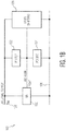
- Figure 2 is a third example 200 of the apparatus for charge recycling.
- the apparatus 200 includes: a first power-delivery circuit 202; a top power-domain 204; a second power-delivery circuit 206; a bottom power-domain 208; and a signal level-shifter circuit 210.
- the first power-delivery circuit 202 includes: a top-power-domain-node voltage output 212 (Vhigh); a mid-power-domain-node voltage output 214 (Vmid); and a ground-node voltage output 216 (Vgnd).
- the top power-domain 204 nominally operates at a top-domain voltage (Vtop) and is coupled to receive the top-node voltage output 212 (Vhigh).
- the second power-delivery circuit 206 is coupled to receive the mid-node voltage output 214 (Vmid) and to a low-side output 218 from the top power-domain 204. In combination with the first power-delivery circuit 202, the second power-delivery circuit 206 maintains the top-domain voltage (Vtop).
- the second power-delivery circuit 206 also includes a low-node voltage output 220 (Vlow).
- the bottom power-domain 208 nominally operates at a bottom-domain voltage (Vbottom) and is coupled to receive the low-node voltage output 220 (Vlow) and to the ground-node voltage output 216 (Vgnd). In combination with the first power-delivery circuit 202, the second power-delivery circuit 206 maintains the bottom-domain voltage (Vbottom).
- the signal level-shifter circuit 210 translates signal voltage levels between the top and bottom power-domains 204, 208.
- the top and bottom power-domains 204, 208 are isolated from each other by the second power-delivery circuit 206, and thus this example apparatus 200 can be applied to voltage-supply noise sensitive applications such as analog and or RF. Due to this isolation, in one example embodiment the top power-domain 204 can be a digital circuit (e.g. an MCU and/or DSP) which generates EMI/noise and the bottom power-domain 208 can be an analog circuit (e.g. radio) needing isolation from such EMI/noise.
- a digital circuit e.g. an MCU and/or DSP
- the bottom power-domain 208 can be an analog circuit (e.g. radio) needing isolation from such EMI/noise.
- the second power-delivery circuit 206 may up or down convert the Vmid 214 voltage to maintain Vtop and Vbottom. With this example apparatus 200, the voltage integrity of top and bottom power-domains 204, 208 are independently maintained. In applications where Vhigh is sufficiently large, the first power-delivery circuit may not need to include an up or down voltage-converter. Thus in one example embodiment, where the first power-delivery circuit 202 is a battery, the overall stacked power-domain apparatus 200 can be optimized for an overall cycle of the battery.
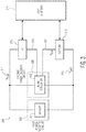
- Figure 3 is a fourth example 300 of the apparatus for charge recycling.
- the apparatus 300 includes: a first power-delivery circuit 302 having a battery 304; a top power-domain 306; a second power-delivery circuit 308; a bottom power-domain 310; and a signal level-shifter circuit 312.
- the first power-delivery circuit 302 includes: a top-power-domain-node voltage output 314 (Vhigh); and a ground-node voltage output 316 (Vgnd).
- the top power-domain 306 nominally operates at a top-domain voltage (Vtop) and is coupled to receive the top-node voltage output 314 (Vhigh).
- the second power-delivery circuit 308 is coupled to receive the top-node voltage output 314 (Vhigh) and to a low-side output 318 from the top power-domain 306. In combination with the first power-delivery circuit 302, the second power-delivery circuit 308 maintains the top-domain voltage (Vtop).
- the second power-delivery circuit 308 also includes: a low-node voltage output 320 (Vlow); and a linear regulator 322.
- the bottom power-domain 310 nominally operates at a bottom-domain voltage (Vbottom) and is coupled to receive the low-node voltage output 320 (Vlow) and to the ground-node voltage output 316 (Vgnd). In combination with the first power-delivery circuit 302, the second power-delivery circuit 308 maintains the bottom-domain voltage (Vbottom).
- the signal level-shifter circuit 312 translates signal voltage levels between the top and bottom power-domains 306, 310.
- the second power-delivery circuit 308 isolates the top and bottom power-domains 306, 310 and thus this apparatus 300 can be applied to voltage-supply noise sensitive applications such as analog and or RF.
- the second power-delivery circuit 308 uses linear regulator 322 which can sink the noise between the top and bottom power-domains.
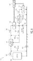
- FIG. 4 is a fifth example 400 of the apparatus for charge recycling.
- the apparatus 400 includes: a battery 402; a first power-delivery circuit 404 (e.g. power-delivery1); a top power-domain 406; a buffer capacitance 408 (i.e. an energy storage element); a second power-delivery circuit 410 (e.g. power-delivery2); a bottom power-domain 412; and a signal level-shifter circuit 414.
- the battery 402 outputs Vbattery 416 resulting in VDDbattery 418 with respect to GND 420.
- the first power-delivery circuit 404 inputs Vbattery 416 and outputs Vhigh 422 and Vmid 424. The difference between Vhigh 422 and Vmid 424 is VDDtop 426. Thus the first power-delivery circuit 404 maintains the top-domain voltage VDDtop 426.
- the top power-domain 406 nominally operates at VDDtop 426 and is coupled to receive Vhigh 422 and Vmid 424.
- the buffer capacitance 408 (i.e. an energy storage element) is coupled between Vmid 424 and GND 420.
- the buffer capacitance 408 stores charge for later use by the first or second power-delivery circuits 404, 410 as necessary to maintain sufficient voltages Vhigh 422, Vmid 424 and Vlow 428 with respect to GND 420.
- the buffer capacitance 408 has a magnitude at least three times greater than a total system capacitance, so as to provide sufficient charge to the second power-delivery circuit 410 if needed.
- the second power-delivery circuit 410 is coupled to receive Vmid 424 and to output Vlow 428.
- the difference between Vlow 428 and GND 420 is VDDbottom 430.
- Either or both the first and second power-delivery circuits 404, 410 can incorporate up or down voltage-converters as needed, depending upon an implementation of the example apparatus 400.
- the bottom power-domain 412 nominally operates at VDDbottom 430 and is coupled to receive Vlow 428 and to GND 420.
- the second power-delivery circuit 410 maintains the bottom-domain voltage VDDbottom 430.
- the signal level-shifter circuit 414 translates signal voltage levels between the top and bottom power-domains 406, 412.
- Vmid 424 is adjusted (e.g. up or down converted) by the second power-delivery circuit 410 (e.g. power-delivery2) so as to set Vlow 428 to the correct VDDbottom 430 value for the bottom power-domain 412.
- the second power-delivery circuit 410 incorporates a boost converter topology based on a switch mode supply (e.g. switch capacitor converter) resulting in VDDtop + VDDbottom ⁇ Vbattery.
- a switch mode supply e.g. switch capacitor converter
- FIG. 5 is a sixth example 500 of the apparatus for charge recycling.
- the apparatus 500 includes: a battery 502; a first power-delivery circuit 504 (e.g. power-delivery1); a top power-domain 506; a buffer capacitance 508 (i.e. an energy storage element); a second power-delivery circuit 510 (e.g. power-delivery2); and a bottom power-domain 512.
- a signal level-shifter circuit is not shown.
- the sixth example 500 apparatus parallels that of the fifth example 400 of the apparatus in operation, but is instead shown in an example modeled system topology.
- the first power-delivery circuit 504 includes an out1-pin 514 coupled to the top power-domain 506, buffer capacitance 508, and second power-delivery circuit 510.
- Figures 6A and 6B are example graphs of select currents in the apparatus for charge recycling as applied to the sixth example 500 of the apparatus. These graphs have been generated based in the following operational parameters:
- Figure 6A shows a current (Iout1) on the out1-pin 514 of the first power-delivery circuit 504, verses the top power-domain 506 current (Itop), for three values of the bottom power-domain 512 current (Ibottom).
- Itop is swept from 1mA to 2mA for fixed Ibottom values of 0.8mA, 1mA, and 1.2mA. In this example, when Ibottom is more than Itop, then current is sourced by the out1-pin 514.
- Figure 6B shows a current (Ibattery) provided by the battery 502 to the first power-delivery circuit 504, verses the top power-domain 506 current (Itop), for three values of the bottom power-domain 512 current (Ibottom)
Landscapes
- Engineering & Computer Science (AREA)
- Power Engineering (AREA)
- Charge And Discharge Circuits For Batteries Or The Like (AREA)
- Secondary Cells (AREA)
Abstract
Description
- The present specification relates to systems, methods, apparatuses, devices, articles of manufacture and an architecture for charge recycling.
- According to an example embodiment, an apparatus for charge recycling between a first power-domain operating at a first voltage and a second power-domain operating at a second voltage, comprising: a first power-delivery circuit configured to supply the first voltage to the first power-domain; and a second power-delivery circuit coupled to receive power from both the first power-delivery circuit and the first power-domain; wherein the second power-delivery circuit is configured to supply the second voltage to the second power-domain.
- In another example embodiment, the first voltage plus the second voltage is greater than a maximum operational voltage of the first power-delivery circuit.
- In another example embodiment, the second power-delivery circuit is configured to be coupled between the first power-domain and the second power-domain.
- In another example embodiment, the second power-delivery circuit is configured to isolate the first and second power-domains from each other.
- In another example embodiment, one of the first or second power-domains include a digital circuit and another of the first or second power-domains include an analog circuit.
- In another example embodiment, the first power-delivery circuit includes a battery.
- In another example embodiment, the second power-delivery circuit includes either a boost converter or a switch mode power supply.
- In another example embodiment, at least one of the power-delivery circuits includes an up voltage-converter or down voltage-converter.
- In another example embodiment, the second power-delivery circuit includes either a linear regulator.
- In another example embodiment, further comprising an energy storage element configured to exchange power with the second power-delivery circuit.
- In another example embodiment, the energy storage element and the second power-delivery circuit are configured to source or sink current with respect to either the first power-delivery circuit or the first power-domain.
- In another example embodiment, the energy storage element is a capacitor.
- In another example embodiment, the capacitor includes a capacitance at least at least three orders of magnitude greater than a total capacitance of the apparatus.
- In another example embodiment, further comprising a set of level-shifters configured to translate voltage levels between the first and second power-domains.
- The above discussion is not intended to represent every example embodiment or every implementation within the scope of the current or future Claim sets. The Figures and Detailed Description that follow also exemplify various example embodiments.
- Various example embodiments may be more completely understood in consideration of the following Detailed Description in connection with the accompanying Drawings, in which:
-
-
Figures 1A and1B are first and second examples of an apparatus for charge recycling. -
Figure 2 is a third example of the apparatus for charge recycling. -
Figure 3 is a fourth example of the apparatus for charge recycling. -
Figure 4 is a fifth example of the apparatus for charge recycling. -
Figure 5 is a sixth example of the apparatus for charge recycling. -
Figures 6A and6B are example graphs of select currents in the apparatus for charge recycling. - While the disclosure is amenable to various modifications and alternative forms, specifics thereof have been shown by way of example in the drawings and will be described in detail. It should be understood, however, that other embodiments, beyond the particular embodiments described, are possible as well. All modifications, equivalents, and alternative embodiments falling within the spirit and scope of the appended claims are covered as well.
-
Figures 1A and1B are first 100 and second 102 examples of an apparatus for charge recycling. Charge recycling reduces a circuit's overall energy consumption which is useful for variety of low power circuit designs. The first example 100 inFigure 1A shows an energy-recycling circuit architecture based on stacked power-domains for static and dynamic power reduction. Such example 100 could be implemented as a stacked memory on top of logic (MToL) set of IP-block power-domains in a digital SOC (System on a Chip) device. - The first example 100 apparatus for charge recycling in
Figure 1A includes: aground 104; abattery 106; a power-delivery circuit 108; a top power-domain 110; a bottom power-domain 112; and a signal level-shifter circuit 114. - The
battery 106 is coupled to theground 104 and has a first battery voltage (Vbattery/VDDbattery). The power-delivery circuit 108 includes abattery voltage input 116 for receiving Vbattery/VDDbattery. The power-delivery circuit 108 also includes a top-node voltage output 118, for outputting Vhigh and amid-node voltage output 120 for outputting Vmid. - The top power-
domain 110 nominally operates at a top-domain voltage 122 (Vtop) and is coupled to receive the top-node voltage output 118 (Vhigh) and the mid-node voltage output 120 (Vmid). - The bottom power-
domain 112 nominally operates at a bottom-domain voltage 124 (Vbottom) and is coupled to receive the mid-node voltage output 120 (Vmid) and to theground 104. - The signal level-
shifter circuit 114 translates signal voltage levels between the top and bottom power-domains - In one example, the power-
delivery circuit 108 includes a voltage regulator (e.g. a linear dropout power-converter, a switch mode power supply, or a switched capacitor circuit (SCC)) which converts the battery voltage (Vbattery) to voltage levels Vhigh, Vmid). - In this architecture in Vbattery/VDDbattery from the
battery 106 is more than the sum of voltages of the individual top and bottom power-domain - Note that the mid-node voltage (Vmid), which is sourcing current to one domain and sinking current from another domain, may be exposed to switching or other noise from either the power-
delivery circuit 108 or the top and bottom power-domain domains - For example, the battery voltage can go as low as 1.6V, while performance demands may require that the individual top and bottom power-
domains Figure 1A may not work. - Such a situation can get even more pronounced for certain MCU designs which operate over a range of battery supply voltages (1.6V - 5.5V). Thus for the architecture shown in
Figure 1A , Vmid in one example needs to be carefully regulated so as to ensure the voltage integrity of Vmid and ensure timing closure for the IP-blocks in the top and bottom power-domains - The second example 102 apparatus for charge recycling in
Figure 1B includes: aground 126; anexternal supply 128; a voltage regulator (VR) 130; a top power-domain 132; a bottom power-domain 134; and a signal level-shifter circuit 136. In this example 102 theexternal supply 128 could be a battery which powers the top power-domain 132 and thevoltage regulator 130, which maintains Vmid. This second example 102 however operates in a manner similar to the first example 100 inFigure 1A . -
Figure 2 is a third example 200 of the apparatus for charge recycling. Theapparatus 200 includes: a first power-delivery circuit 202; a top power-domain 204; a second power-delivery circuit 206; a bottom power-domain 208; and a signal level-shifter circuit 210. - The first power-
delivery circuit 202 includes: a top-power-domain-node voltage output 212 (Vhigh); a mid-power-domain-node voltage output 214 (Vmid); and a ground-node voltage output 216 (Vgnd). - The top power-
domain 204 nominally operates at a top-domain voltage (Vtop) and is coupled to receive the top-node voltage output 212 (Vhigh). - The second power-
delivery circuit 206 is coupled to receive the mid-node voltage output 214 (Vmid) and to a low-side output 218 from the top power-domain 204. In combination with the first power-delivery circuit 202, the second power-delivery circuit 206 maintains the top-domain voltage (Vtop). The second power-delivery circuit 206 also includes a low-node voltage output 220 (Vlow). - The bottom power-
domain 208 nominally operates at a bottom-domain voltage (Vbottom) and is coupled to receive the low-node voltage output 220 (Vlow) and to the ground-node voltage output 216 (Vgnd). In combination with the first power-delivery circuit 202, the second power-delivery circuit 206 maintains the bottom-domain voltage (Vbottom). - The signal level-
shifter circuit 210 translates signal voltage levels between the top and bottom power-domains - In this example 200, the top and bottom power-
domains delivery circuit 206, and thus thisexample apparatus 200 can be applied to voltage-supply noise sensitive applications such as analog and or RF. Due to this isolation, in one example embodiment the top power-domain 204 can be a digital circuit (e.g. an MCU and/or DSP) which generates EMI/noise and the bottom power-domain 208 can be an analog circuit (e.g. radio) needing isolation from such EMI/noise. - The second power-
delivery circuit 206 may up or down convert theVmid 214 voltage to maintain Vtop and Vbottom. With thisexample apparatus 200, the voltage integrity of top and bottom power-domains delivery circuit 202 is a battery, the overall stacked power-domain apparatus 200 can be optimized for an overall cycle of the battery. -
Figure 3 is a fourth example 300 of the apparatus for charge recycling. Theapparatus 300 includes: a first power-delivery circuit 302 having abattery 304; a top power-domain 306; a second power-delivery circuit 308; a bottom power-domain 310; and a signal level-shifter circuit 312. - The first power-
delivery circuit 302 includes: a top-power-domain-node voltage output 314 (Vhigh); and a ground-node voltage output 316 (Vgnd). - The top power-
domain 306 nominally operates at a top-domain voltage (Vtop) and is coupled to receive the top-node voltage output 314 (Vhigh). - The second power-
delivery circuit 308 is coupled to receive the top-node voltage output 314 (Vhigh) and to a low-side output 318 from the top power-domain 306. In combination with the first power-delivery circuit 302, the second power-delivery circuit 308 maintains the top-domain voltage (Vtop). The second power-delivery circuit 308 also includes: a low-node voltage output 320 (Vlow); and alinear regulator 322. - The bottom power-
domain 310 nominally operates at a bottom-domain voltage (Vbottom) and is coupled to receive the low-node voltage output 320 (Vlow) and to the ground-node voltage output 316 (Vgnd). In combination with the first power-delivery circuit 302, the second power-delivery circuit 308 maintains the bottom-domain voltage (Vbottom). - The signal level-
shifter circuit 312 translates signal voltage levels between the top and bottom power-domains - In a manner similar to that discussed with respect to
Figure 2 , the second power-delivery circuit 308 isolates the top and bottom power-domains apparatus 300 can be applied to voltage-supply noise sensitive applications such as analog and or RF. - In one example embodiment, the second power-
delivery circuit 308 useslinear regulator 322 which can sink the noise between the top and bottom power-domains. -
Figure 4 is a fifth example 400 of the apparatus for charge recycling. Theapparatus 400 includes: abattery 402; a first power-delivery circuit 404 (e.g. power-delivery1); a top power-domain 406; a buffer capacitance 408 (i.e. an energy storage element); a second power-delivery circuit 410 (e.g. power-delivery2); a bottom power-domain 412; and a signal level-shifter circuit 414. - The
battery 402outputs Vbattery 416 resulting inVDDbattery 418 with respect toGND 420. - The first power-
delivery circuit 404 inputs Vbattery 416 and outputs Vhigh 422 andVmid 424. The difference betweenVhigh 422 andVmid 424 isVDDtop 426. Thus the first power-delivery circuit 404 maintains the top-domain voltage VDDtop 426. - The top power-
domain 406 nominally operates atVDDtop 426 and is coupled to receiveVhigh 422 andVmid 424. - The buffer capacitance 408 (i.e. an energy storage element) is coupled between
Vmid 424 andGND 420. Thebuffer capacitance 408 stores charge for later use by the first or second power-delivery circuits sufficient voltages Vhigh 422,Vmid 424 andVlow 428 with respect toGND 420. - In one example embodiment, the
buffer capacitance 408 has a magnitude at least three times greater than a total system capacitance, so as to provide sufficient charge to the second power-delivery circuit 410 if needed. - The second power-
delivery circuit 410 is coupled to receiveVmid 424 and tooutput Vlow 428. The difference betweenVlow 428 andGND 420 isVDDbottom 430. - Either or both the first and second power-
delivery circuits example apparatus 400. - The bottom power-
domain 412 nominally operates at VDDbottom 430 and is coupled to receiveVlow 428 and toGND 420. The second power-delivery circuit 410 maintains the bottom-domain voltage VDDbottom 430. - The signal level-
shifter circuit 414 translates signal voltage levels between the top and bottom power-domains - In one example,
Vmid 424 is adjusted (e.g. up or down converted) by the second power-delivery circuit 410 (e.g. power-delivery2) so as to setVlow 428 to thecorrect VDDbottom 430 value for the bottom power-domain 412. - In another example embodiment, the second power-
delivery circuit 410 incorporates a boost converter topology based on a switch mode supply (e.g. switch capacitor converter) resulting in VDDtop + VDDbottom ≥ Vbattery. -
Figure 5 is a sixth example 500 of the apparatus for charge recycling. Theapparatus 500 includes: abattery 502; a first power-delivery circuit 504 (e.g. power-delivery1); a top power-domain 506; a buffer capacitance 508 (i.e. an energy storage element); a second power-delivery circuit 510 (e.g. power-delivery2); and a bottom power-domain 512. A signal level-shifter circuit is not shown. - The sixth example 500 apparatus parallels that of the fifth example 400 of the apparatus in operation, but is instead shown in an example modeled system topology. The first power-
delivery circuit 504 includes an out1-pin 514 coupled to the top power-domain 506,buffer capacitance 508, and second power-delivery circuit 510. -
Figures 6A and6B are example graphs of select currents in the apparatus for charge recycling as applied to the sixth example 500 of the apparatus. These graphs have been generated based in the following operational parameters: - ∘
battery 502 voltage of 1.8V; - ∘ top power-
domain 506 requiring 1V and consuming average current (Itop); - ∘ bottom power-
domain 512 requiring 1V and consuming average current (Ibottom); - ∘ first power-
delivery circuit 504 using a low-dropout regulator/power-converter (LDO) providing Vhigh = 1.8V;- ▪ first power-
delivery circuit 504 maintains 1V across the top power-domain 504, thus Vmid= 0.8V;
- ▪ first power-
- ∘ second power-
delivery circuit 510 uses the 0.8 V Vmid voltage and converts into Vlow = 1V at 75% power-conversion efficiency. -
Figure 6A shows a current (Iout1) on the out1-pin 514 of the first power-delivery circuit 504, verses the top power-domain 506 current (Itop), for three values of the bottom power-domain 512 current (Ibottom). - Note, in
Figure 6A , the current sourced/supplied by the out1-pin 514 (Iout1) to the first power-delivery circuit 504 is shown in the graph as negative, while the current drained/sunk by the first power-delivery circuit 504 from thebuffer capacitance 508 is shown as positive. - Itop is swept from 1mA to 2mA for fixed Ibottom values of 0.8mA, 1mA, and 1.2mA. In this example, when Ibottom is more than Itop, then current is sourced by the out1-
pin 514. -
Figure 6B shows a current (Ibattery) provided by thebattery 502 to the first power-delivery circuit 504, verses the top power-domain 506 current (Itop), for three values of the bottom power-domain 512 current (Ibottom) - While the example embodiments discussed herein pertain to a set of stacked (i.e. shared current) power-domains, these techniques can also be used for flat (i.e. shared voltage) circuit designs. Also, while these example embodiments discuss power management techniques for just two stacked power-domains, these techniques can be scaled to three or more power-domains as well.
- In this specification, example embodiments have been presented in terms of a selected set of details. However, a person of ordinary skill in the art would understand that many other example embodiments may be practiced which include a different selected set of these details. It is intended that the following claims cover all possible example embodiments.
Claims (14)
- An apparatus for charge recycling between a first power-domain operating at a first voltage and a second power-domain operating at a second voltage, comprising:a first power-delivery circuit configured to supply the first voltage to the first power-domain; anda second power-delivery circuit coupled to receive power from both the first power-delivery circuit and the first power-domain;wherein the second power-delivery circuit is configured to supply the second voltage to the second power-domain.
- The apparatus of claim 1:wherein the first voltage plus the second voltage is greater than a maximum operational voltage of the first power-delivery circuit.
- The apparatus of claim 1 or 2:wherein the second power-delivery circuit is configured to be coupled between the first power-domain and the second power-domain.
- The apparatus of any preceding claim:wherein the second power-delivery circuit is configured to isolate the first and second power-domains from each other.
- The apparatus of any preceding claim:wherein one of the first or second power-domains include a digital circuit and another of the first or second power-domains include an analog circuit.
- The apparatus of any preceding claim:wherein the first power-delivery circuit includes a battery.
- The apparatus of any preceding claim:wherein the second power-delivery circuit includes either a boost converter or a switch mode power supply.
- The apparatus of any preceding claim:wherein at least one of the power-delivery circuits includes an up voltage-converter or down voltage-converter.
- The apparatus of any preceding claim:wherein the second power-delivery circuit includes either a linear regulator.
- The apparatus of any preceding claim:further comprising an energy storage element configured to exchange power with the second power-delivery circuit.
- The apparatus of claim 10:wherein the energy storage element and the second power-delivery circuit are configured to source or sink current with respect to either the first power-delivery circuit or the first power-domain.
- The apparatus of claim 10 or 11:wherein the energy storage element is a capacitor.
- The apparatus of claim 12:wherein the capacitor includes a capacitance at least at least three orders of magnitude greater than a total capacitance of the apparatus.
- The apparatus of any preceding claim:further comprising a set of level-shifters configured to translate voltage levels between the first and second power-domains.
Applications Claiming Priority (1)
| Application Number | Priority Date | Filing Date | Title |
|---|---|---|---|
| US15/052,509 US9960670B2 (en) | 2016-03-11 | 2016-03-11 | Apparatus for charge recycling |
Publications (2)
| Publication Number | Publication Date |
|---|---|
| EP3217526A1 true EP3217526A1 (en) | 2017-09-13 |
| EP3217526B1 EP3217526B1 (en) | 2019-08-07 |
Family
ID=58412846
Family Applications (1)
| Application Number | Title | Priority Date | Filing Date |
|---|---|---|---|
| EP17158735.5A Active EP3217526B1 (en) | 2016-03-11 | 2017-03-01 | Apparatus for charge-recycling |
Country Status (3)
| Country | Link |
|---|---|
| US (1) | US9960670B2 (en) |
| EP (1) | EP3217526B1 (en) |
| CN (1) | CN107181402B (en) |
Families Citing this family (2)
| Publication number | Priority date | Publication date | Assignee | Title |
|---|---|---|---|---|
| TWI682634B (en) | 2018-11-06 | 2020-01-11 | 崛智科技有限公司 | Integrated circuitry |
| US11669135B2 (en) * | 2021-08-16 | 2023-06-06 | DXCorr Design Inc. | Inter-chip input-output (IO) for voltage-stacked near threshold computing (NTC) chips |
Citations (5)
| Publication number | Priority date | Publication date | Assignee | Title |
|---|---|---|---|---|
| US20050127756A1 (en) * | 2003-05-08 | 2005-06-16 | The Trustees Of Columbia University | Charge-recycling voltage domains for energy-efficient low-voltage operation of digital CMOS circuits |
| US20110298440A1 (en) * | 2010-06-07 | 2011-12-08 | International Business Machines Corporation | Low voltage signaling |
| US20130131771A1 (en) * | 2010-07-30 | 2013-05-23 | Torsten Lehmann | Current recycling in multiple linear regulators |
| US20140268917A1 (en) * | 2013-03-14 | 2014-09-18 | Analog Devices Technology | Isolated error amplifier for isolated power supplies |
| US20150355662A1 (en) * | 2014-06-05 | 2015-12-10 | Arm Limited | Power Gating in an Electronic Device |
Family Cites Families (17)
| Publication number | Priority date | Publication date | Assignee | Title |
|---|---|---|---|---|
| JP3300593B2 (en) | 1995-06-15 | 2002-07-08 | 株式会社東芝 | Semiconductor integrated circuit device |
| US6864668B1 (en) * | 1999-02-09 | 2005-03-08 | Tropian, Inc. | High-efficiency amplifier output level and burst control |
| KR100362700B1 (en) * | 2000-02-03 | 2002-11-27 | 삼성전자 주식회사 | Voltage regulator circuit built in a semiconductor memory device |
| US6479974B2 (en) * | 2000-12-28 | 2002-11-12 | International Business Machines Corporation | Stacked voltage rails for low-voltage DC distribution |
| US7702929B2 (en) | 2004-11-29 | 2010-04-20 | Marvell World Trade Ltd. | Low voltage logic operation using higher voltage supply levels |
| US20080042722A1 (en) * | 2006-08-15 | 2008-02-21 | Silicon Laboratories, Inc. | High speed level shifter circuit and circuit using same |
| US7735030B1 (en) * | 2007-02-28 | 2010-06-08 | Cadence Design Systems, Inc. | Simulating restorable registers in power domain systems |
| US8339176B2 (en) * | 2008-05-30 | 2012-12-25 | Infineon Technologies Ag | System and method for providing a low-power self-adjusting reference current for floating supply stages |
| US8174288B2 (en) * | 2009-04-13 | 2012-05-08 | International Business Machines Corporation | Voltage conversion and integrated circuits with stacked voltage domains |
| US8476962B2 (en) | 2009-11-18 | 2013-07-02 | Freescale Semiconductor, Inc. | System having multiple voltage tiers and method therefor |
| US8751833B2 (en) * | 2010-04-30 | 2014-06-10 | Arm Limited | Data processing system |
| US8339177B2 (en) | 2011-01-26 | 2012-12-25 | Freescale Semiconductor, Inc. | Multiple function power domain level shifter |
| US8878387B1 (en) | 2013-05-16 | 2014-11-04 | Micrel, Inc. | Multi-level stack voltage system for integrated circuits |
| US20150346742A1 (en) | 2014-06-02 | 2015-12-03 | Nxp B.V. | Energy recycling for a cost effective platform to optimize energy efficiency for low powered system |
| US9787310B2 (en) * | 2014-12-17 | 2017-10-10 | Silicon Laboratories Inc. | Level-shifter circuit for low-input voltages |
| CN104765400B (en) * | 2015-02-05 | 2017-02-01 | 武汉大学 | Photovoltaic power generation system environment self-adaptive type MPPT (maximum power point tracking) method and system |
| CN106558987B (en) * | 2015-09-29 | 2019-12-20 | 意法半导体(中国)投资有限公司 | Low quiescent current linear regulator circuit |
-
2016
- 2016-03-11 US US15/052,509 patent/US9960670B2/en active Active
-
2017
- 2017-03-01 EP EP17158735.5A patent/EP3217526B1/en active Active
- 2017-03-09 CN CN201710139610.3A patent/CN107181402B/en active Active
Patent Citations (5)
| Publication number | Priority date | Publication date | Assignee | Title |
|---|---|---|---|---|
| US20050127756A1 (en) * | 2003-05-08 | 2005-06-16 | The Trustees Of Columbia University | Charge-recycling voltage domains for energy-efficient low-voltage operation of digital CMOS circuits |
| US20110298440A1 (en) * | 2010-06-07 | 2011-12-08 | International Business Machines Corporation | Low voltage signaling |
| US20130131771A1 (en) * | 2010-07-30 | 2013-05-23 | Torsten Lehmann | Current recycling in multiple linear regulators |
| US20140268917A1 (en) * | 2013-03-14 | 2014-09-18 | Analog Devices Technology | Isolated error amplifier for isolated power supplies |
| US20150355662A1 (en) * | 2014-06-05 | 2015-12-10 | Arm Limited | Power Gating in an Electronic Device |
Also Published As
| Publication number | Publication date |
|---|---|
| CN107181402A (en) | 2017-09-19 |
| US9960670B2 (en) | 2018-05-01 |
| EP3217526B1 (en) | 2019-08-07 |
| US20170264189A1 (en) | 2017-09-14 |
| CN107181402B (en) | 2021-06-04 |
Similar Documents
| Publication | Publication Date | Title |
|---|---|---|
| EP3202025B1 (en) | A multiple output boost dc-dc power converter | |
| TWI767399B (en) | Voltage regulator with piecewise linear loadlines | |
| KR101991366B1 (en) | Electric power management apparatus and multi-source energy harvesting system using the same | |
| US11190097B2 (en) | Voltage converter | |
| KR101358411B1 (en) | Computer and power supply method thereof | |
| US10312709B2 (en) | Multi-configurable switch mode charging system, charging circuit, and charging method | |
| EP3540555A1 (en) | Output voltage regulation device and method | |
| TWI673946B (en) | Power supply and method of precise voltage position using dc-dc converter | |
| US9059643B2 (en) | Switching configuration and method for the production of an alternating voltage from at least supply terminals with temporally variable output DC voltage | |
| KR20160117239A (en) | Power supply system and energy storage system | |
| JP2009106050A (en) | Overvoltage protection circuit | |
| US8384356B2 (en) | Self contained power source | |
| US10622814B2 (en) | Power conversion apparatus | |
| US9960670B2 (en) | Apparatus for charge recycling | |
| AU2018401837B2 (en) | System for powering auxiliary loads of an energy storage system | |
| Kularatna et al. | A supercapacitor technique for efficiency improvement in linear regulators | |
| CN114223106A (en) | Electric energy storage device, control device and electric energy storage system | |
| US9960636B2 (en) | Power supply system and direct-current converter thereof | |
| Takahashi et al. | Droop control for bi-directional DC-DC converters used in multi-level virtual conductors | |
| Peyghami-Akhuleh et al. | A new secondary control approach for voltage regulation in DC microgrids | |
| RU2680245C1 (en) | Spacecraft power supply system | |
| US10965217B2 (en) | Power conversion apparatus | |
| US6894462B1 (en) | Ratio adaptive gated oscillator | |
| JP6896203B2 (en) | Rectifier circuit, DC power supply synthesis circuit, and full-wave rectifier circuit | |
| Hsu et al. | A Single-Inductor Dual-Output DC-DC Converter with Dual-Mode Control |
Legal Events
| Date | Code | Title | Description |
|---|---|---|---|
| PUAI | Public reference made under article 153(3) epc to a published international application that has entered the european phase |
Free format text: ORIGINAL CODE: 0009012 |
|
| STAA | Information on the status of an ep patent application or granted ep patent |
Free format text: STATUS: THE APPLICATION HAS BEEN PUBLISHED |
|
| AK | Designated contracting states |
Kind code of ref document: A1 Designated state(s): AL AT BE BG CH CY CZ DE DK EE ES FI FR GB GR HR HU IE IS IT LI LT LU LV MC MK MT NL NO PL PT RO RS SE SI SK SM TR |
|
| AX | Request for extension of the european patent |
Extension state: BA ME |
|
| STAA | Information on the status of an ep patent application or granted ep patent |
Free format text: STATUS: REQUEST FOR EXAMINATION WAS MADE |
|
| 17P | Request for examination filed |
Effective date: 20180313 |
|
| RBV | Designated contracting states (corrected) |
Designated state(s): AL AT BE BG CH CY CZ DE DK EE ES FI FR GB GR HR HU IE IS IT LI LT LU LV MC MK MT NL NO PL PT RO RS SE SI SK SM TR |
|
| STAA | Information on the status of an ep patent application or granted ep patent |
Free format text: STATUS: EXAMINATION IS IN PROGRESS |
|
| 17Q | First examination report despatched |
Effective date: 20180713 |
|
| GRAP | Despatch of communication of intention to grant a patent |
Free format text: ORIGINAL CODE: EPIDOSNIGR1 |
|
| STAA | Information on the status of an ep patent application or granted ep patent |
Free format text: STATUS: GRANT OF PATENT IS INTENDED |
|
| INTG | Intention to grant announced |
Effective date: 20190320 |
|
| GRAS | Grant fee paid |
Free format text: ORIGINAL CODE: EPIDOSNIGR3 |
|
| GRAA | (expected) grant |
Free format text: ORIGINAL CODE: 0009210 |
|
| STAA | Information on the status of an ep patent application or granted ep patent |
Free format text: STATUS: THE PATENT HAS BEEN GRANTED |
|
| AK | Designated contracting states |
Kind code of ref document: B1 Designated state(s): AL AT BE BG CH CY CZ DE DK EE ES FI FR GB GR HR HU IE IS IT LI LT LU LV MC MK MT NL NO PL PT RO RS SE SI SK SM TR |
|
| REG | Reference to a national code |
Ref country code: GB Ref legal event code: FG4D |
|
| REG | Reference to a national code |
Ref country code: CH Ref legal event code: EP Ref country code: AT Ref legal event code: REF Ref document number: 1165336 Country of ref document: AT Kind code of ref document: T Effective date: 20190815 |
|
| REG | Reference to a national code |
Ref country code: DE Ref legal event code: R096 Ref document number: 602017005779 Country of ref document: DE |
|
| REG | Reference to a national code |
Ref country code: IE Ref legal event code: FG4D |
|
| REG | Reference to a national code |
Ref country code: NL Ref legal event code: MP Effective date: 20190807 |
|
| REG | Reference to a national code |
Ref country code: LT Ref legal event code: MG4D |
|
| PG25 | Lapsed in a contracting state [announced via postgrant information from national office to epo] |
Ref country code: NO Free format text: LAPSE BECAUSE OF FAILURE TO SUBMIT A TRANSLATION OF THE DESCRIPTION OR TO PAY THE FEE WITHIN THE PRESCRIBED TIME-LIMIT Effective date: 20191107 Ref country code: PT Free format text: LAPSE BECAUSE OF FAILURE TO SUBMIT A TRANSLATION OF THE DESCRIPTION OR TO PAY THE FEE WITHIN THE PRESCRIBED TIME-LIMIT Effective date: 20191209 Ref country code: SE Free format text: LAPSE BECAUSE OF FAILURE TO SUBMIT A TRANSLATION OF THE DESCRIPTION OR TO PAY THE FEE WITHIN THE PRESCRIBED TIME-LIMIT Effective date: 20190807 Ref country code: FI Free format text: LAPSE BECAUSE OF FAILURE TO SUBMIT A TRANSLATION OF THE DESCRIPTION OR TO PAY THE FEE WITHIN THE PRESCRIBED TIME-LIMIT Effective date: 20190807 Ref country code: HR Free format text: LAPSE BECAUSE OF FAILURE TO SUBMIT A TRANSLATION OF THE DESCRIPTION OR TO PAY THE FEE WITHIN THE PRESCRIBED TIME-LIMIT Effective date: 20190807 Ref country code: LT Free format text: LAPSE BECAUSE OF FAILURE TO SUBMIT A TRANSLATION OF THE DESCRIPTION OR TO PAY THE FEE WITHIN THE PRESCRIBED TIME-LIMIT Effective date: 20190807 Ref country code: BG Free format text: LAPSE BECAUSE OF FAILURE TO SUBMIT A TRANSLATION OF THE DESCRIPTION OR TO PAY THE FEE WITHIN THE PRESCRIBED TIME-LIMIT Effective date: 20191107 Ref country code: NL Free format text: LAPSE BECAUSE OF FAILURE TO SUBMIT A TRANSLATION OF THE DESCRIPTION OR TO PAY THE FEE WITHIN THE PRESCRIBED TIME-LIMIT Effective date: 20190807 |
|
| REG | Reference to a national code |
Ref country code: AT Ref legal event code: MK05 Ref document number: 1165336 Country of ref document: AT Kind code of ref document: T Effective date: 20190807 |
|
| PG25 | Lapsed in a contracting state [announced via postgrant information from national office to epo] |
Ref country code: AL Free format text: LAPSE BECAUSE OF FAILURE TO SUBMIT A TRANSLATION OF THE DESCRIPTION OR TO PAY THE FEE WITHIN THE PRESCRIBED TIME-LIMIT Effective date: 20190807 Ref country code: GR Free format text: LAPSE BECAUSE OF FAILURE TO SUBMIT A TRANSLATION OF THE DESCRIPTION OR TO PAY THE FEE WITHIN THE PRESCRIBED TIME-LIMIT Effective date: 20191108 Ref country code: ES Free format text: LAPSE BECAUSE OF FAILURE TO SUBMIT A TRANSLATION OF THE DESCRIPTION OR TO PAY THE FEE WITHIN THE PRESCRIBED TIME-LIMIT Effective date: 20190807 Ref country code: LV Free format text: LAPSE BECAUSE OF FAILURE TO SUBMIT A TRANSLATION OF THE DESCRIPTION OR TO PAY THE FEE WITHIN THE PRESCRIBED TIME-LIMIT Effective date: 20190807 Ref country code: RS Free format text: LAPSE BECAUSE OF FAILURE TO SUBMIT A TRANSLATION OF THE DESCRIPTION OR TO PAY THE FEE WITHIN THE PRESCRIBED TIME-LIMIT Effective date: 20190807 Ref country code: IS Free format text: LAPSE BECAUSE OF FAILURE TO SUBMIT A TRANSLATION OF THE DESCRIPTION OR TO PAY THE FEE WITHIN THE PRESCRIBED TIME-LIMIT Effective date: 20191207 |
|
| PG25 | Lapsed in a contracting state [announced via postgrant information from national office to epo] |
Ref country code: TR Free format text: LAPSE BECAUSE OF FAILURE TO SUBMIT A TRANSLATION OF THE DESCRIPTION OR TO PAY THE FEE WITHIN THE PRESCRIBED TIME-LIMIT Effective date: 20190807 |
|
| PG25 | Lapsed in a contracting state [announced via postgrant information from national office to epo] |
Ref country code: RO Free format text: LAPSE BECAUSE OF FAILURE TO SUBMIT A TRANSLATION OF THE DESCRIPTION OR TO PAY THE FEE WITHIN THE PRESCRIBED TIME-LIMIT Effective date: 20190807 Ref country code: PL Free format text: LAPSE BECAUSE OF FAILURE TO SUBMIT A TRANSLATION OF THE DESCRIPTION OR TO PAY THE FEE WITHIN THE PRESCRIBED TIME-LIMIT Effective date: 20190807 Ref country code: EE Free format text: LAPSE BECAUSE OF FAILURE TO SUBMIT A TRANSLATION OF THE DESCRIPTION OR TO PAY THE FEE WITHIN THE PRESCRIBED TIME-LIMIT Effective date: 20190807 Ref country code: DK Free format text: LAPSE BECAUSE OF FAILURE TO SUBMIT A TRANSLATION OF THE DESCRIPTION OR TO PAY THE FEE WITHIN THE PRESCRIBED TIME-LIMIT Effective date: 20190807 Ref country code: AT Free format text: LAPSE BECAUSE OF FAILURE TO SUBMIT A TRANSLATION OF THE DESCRIPTION OR TO PAY THE FEE WITHIN THE PRESCRIBED TIME-LIMIT Effective date: 20190807 Ref country code: IT Free format text: LAPSE BECAUSE OF FAILURE TO SUBMIT A TRANSLATION OF THE DESCRIPTION OR TO PAY THE FEE WITHIN THE PRESCRIBED TIME-LIMIT Effective date: 20190807 |
|
| PG25 | Lapsed in a contracting state [announced via postgrant information from national office to epo] |
Ref country code: CZ Free format text: LAPSE BECAUSE OF FAILURE TO SUBMIT A TRANSLATION OF THE DESCRIPTION OR TO PAY THE FEE WITHIN THE PRESCRIBED TIME-LIMIT Effective date: 20190807 Ref country code: IS Free format text: LAPSE BECAUSE OF FAILURE TO SUBMIT A TRANSLATION OF THE DESCRIPTION OR TO PAY THE FEE WITHIN THE PRESCRIBED TIME-LIMIT Effective date: 20200224 Ref country code: SM Free format text: LAPSE BECAUSE OF FAILURE TO SUBMIT A TRANSLATION OF THE DESCRIPTION OR TO PAY THE FEE WITHIN THE PRESCRIBED TIME-LIMIT Effective date: 20190807 Ref country code: SK Free format text: LAPSE BECAUSE OF FAILURE TO SUBMIT A TRANSLATION OF THE DESCRIPTION OR TO PAY THE FEE WITHIN THE PRESCRIBED TIME-LIMIT Effective date: 20190807 |
|
| REG | Reference to a national code |
Ref country code: DE Ref legal event code: R097 Ref document number: 602017005779 Country of ref document: DE |
|
| PLBE | No opposition filed within time limit |
Free format text: ORIGINAL CODE: 0009261 |
|
| STAA | Information on the status of an ep patent application or granted ep patent |
Free format text: STATUS: NO OPPOSITION FILED WITHIN TIME LIMIT |
|
| PG2D | Information on lapse in contracting state deleted |
Ref country code: IS |
|
| 26N | No opposition filed |
Effective date: 20200603 |
|
| PG25 | Lapsed in a contracting state [announced via postgrant information from national office to epo] |
Ref country code: SI Free format text: LAPSE BECAUSE OF FAILURE TO SUBMIT A TRANSLATION OF THE DESCRIPTION OR TO PAY THE FEE WITHIN THE PRESCRIBED TIME-LIMIT Effective date: 20190807 |
|
| PG25 | Lapsed in a contracting state [announced via postgrant information from national office to epo] |
Ref country code: MC Free format text: LAPSE BECAUSE OF FAILURE TO SUBMIT A TRANSLATION OF THE DESCRIPTION OR TO PAY THE FEE WITHIN THE PRESCRIBED TIME-LIMIT Effective date: 20190807 |
|
| REG | Reference to a national code |
Ref country code: CH Ref legal event code: PL |
|
| REG | Reference to a national code |
Ref country code: BE Ref legal event code: MM Effective date: 20200331 |
|
| PG25 | Lapsed in a contracting state [announced via postgrant information from national office to epo] |
Ref country code: LU Free format text: LAPSE BECAUSE OF NON-PAYMENT OF DUE FEES Effective date: 20200301 |
|
| PG25 | Lapsed in a contracting state [announced via postgrant information from national office to epo] |
Ref country code: FR Free format text: LAPSE BECAUSE OF NON-PAYMENT OF DUE FEES Effective date: 20200331 Ref country code: IE Free format text: LAPSE BECAUSE OF NON-PAYMENT OF DUE FEES Effective date: 20200301 Ref country code: LI Free format text: LAPSE BECAUSE OF NON-PAYMENT OF DUE FEES Effective date: 20200331 Ref country code: CH Free format text: LAPSE BECAUSE OF NON-PAYMENT OF DUE FEES Effective date: 20200331 |
|
| PG25 | Lapsed in a contracting state [announced via postgrant information from national office to epo] |
Ref country code: BE Free format text: LAPSE BECAUSE OF NON-PAYMENT OF DUE FEES Effective date: 20200331 |
|
| GBPC | Gb: european patent ceased through non-payment of renewal fee |
Effective date: 20210301 |
|
| PG25 | Lapsed in a contracting state [announced via postgrant information from national office to epo] |
Ref country code: GB Free format text: LAPSE BECAUSE OF NON-PAYMENT OF DUE FEES Effective date: 20210301 |
|
| PG25 | Lapsed in a contracting state [announced via postgrant information from national office to epo] |
Ref country code: MT Free format text: LAPSE BECAUSE OF FAILURE TO SUBMIT A TRANSLATION OF THE DESCRIPTION OR TO PAY THE FEE WITHIN THE PRESCRIBED TIME-LIMIT Effective date: 20190807 Ref country code: CY Free format text: LAPSE BECAUSE OF FAILURE TO SUBMIT A TRANSLATION OF THE DESCRIPTION OR TO PAY THE FEE WITHIN THE PRESCRIBED TIME-LIMIT Effective date: 20190807 |
|
| PG25 | Lapsed in a contracting state [announced via postgrant information from national office to epo] |
Ref country code: MK Free format text: LAPSE BECAUSE OF FAILURE TO SUBMIT A TRANSLATION OF THE DESCRIPTION OR TO PAY THE FEE WITHIN THE PRESCRIBED TIME-LIMIT Effective date: 20190807 |
|
| P01 | Opt-out of the competence of the unified patent court (upc) registered |
Effective date: 20230725 |
|
| PGFP | Annual fee paid to national office [announced via postgrant information from national office to epo] |
Ref country code: DE Payment date: 20260219 Year of fee payment: 10 |